Embed Size (px)
Citation preview

ADP1071-2EBZ12.1V User Guide UG-1129
One Technology Way • P.O. Box 9106 • Norwood, MA 02062-9106, U.S.A. • Tel: 781.329.4700 • Fax: 781.461.3113 • www.analog.com
Evaluating the ADP1071-2 Isolated Synchronous Flyback Controller with Integrated iCoupler
PLEASE SEE THE LAST PAGE FOR AN IMPORTANT WARNING AND LEGAL TERMS AND CONDITIONS. Rev. A | Page 1 of 15
FEATURES Full support evaluation kit for the ADP1071-2 36 W flyback topology 12.1 V output voltage (Vdc) 3 A steady state, 5 A peak Forced CCM operation Dedicated internal primary and secondary side MOSFET
drivers External reference signal tracking Precision enabled undervoltage lockout with hysteresis Short-circuit, output overvoltage, cycle by cycle input
overcurrent, and over temperature protection Frequency synchronization Soft start and soft stop functionality
EVALUATION KIT CONTENTS ADP1071-2EBZ12.1V
ADDITIONAL EQUIPMENT NEEDED DC power supply capable of 36 Vdc to 60 Vdc, 3 A Electronic load capable of 150 W, 0 V to 60 V Oscilloscope capable of ≥500 MHz bandwidth, 2 channels to
4 channels Precision digital multimeter (HP34401 or equivalent)
GENERAL DESCRIPTION The ADP1071-2EBZ12.1V evaluation board allows users to evaluate the ADP1071-2 in a power supply application.
The evaluation board is set up to act as an isolated power supply unit (PSU), with a rated load of 12.1 Vdc, 3 A in steady state (5 A peak) from a 36 Vdc to 60 Vdc source.
Connectors on the ADP1071-2EBZ12.1V provide synchronization, allowing direct paralleling evaluation when multiple ADP1071-2EBZ12.1V evaluation boards are connected in parallel to a common bus.
Multiple test points allow easy access to all critical nodes and pins.
Complete information about the ADP1071-2 is available in the ADP1071-1/ADP1071-2 data sheet, which should be consulted in conjunction with this user guide when using the evaluation board.
ADP1071-2EBZ12.1V EVALUATION BOARD SETUP
Figure 1.
1575
7-00
1

UG-1129 ADP1071-2EBZ12.1V User Guide
Rev. A | Page 2 of 15
TABLE OF CONTENTS Features .............................................................................................. 1 Evaluation Kit Contents ................................................................... 1 Additional Equipment Needed ....................................................... 1 General Description ......................................................................... 1 ADP1071-2EBZ12.1V Evaluation Board Setup ........................... 1 Revision History ............................................................................... 2 Evaluation Board Overview ............................................................ 3
Power Train Overview ................................................................. 3 Applications ................................................................................... 3 Connectors .................................................................................... 3 Caution .......................................................................................... 3
Evaluation Board Hardware ............................................................ 4 Evaluation Board Configurations .............................................. 4 Powering Up .................................................................................. 4 ADP1071-2EBZ12.1V Dimensions............................................ 4
Evaluating the ADP1071-2 ...............................................................5 Gate and SR Pins and Functionality ...........................................5 Soft Start .........................................................................................6 Soft Stop ..........................................................................................6 Output Ripple ................................................................................6 Control Loop ..................................................................................7 External Signal Tracking ..............................................................7 Over Current Protection (OCP) .................................................8 Voltage and Current Stress ...........................................................8 Efficiency Curves ..........................................................................9 Thermal Performance ...................................................................9
Evaluation Board Schematic and Artwork .................................. 10 Ordering Information .................................................................... 14
Bill of Materials ........................................................................... 14
REVISION HISTORY 12/2018—Rev. 0 to Rev A. Change to Figure 21 ....................................................................... 10
10/2018—Revision 0: Initial Version
ADP1071-2EBZ12.1V User Guide UG-1129
Rev. A | Page 3 of 15
EVALUATION BOARD OVERVIEW This evaluation board features the ADP1071-2 in a dc-to-dc switching power supply in flyback topology with synchronous rectification operating at 300 kHz switching frequency.
The ADP1071-2 circuit is designed to provide a rated load of 12.1 Vdc, 3 A from a dc input voltage source of 36 Vdc to 60 Vdc. The ADP1071-2 operates in continuous conduction mode (CCM) and provides features including precision undervoltage lockout (UVLO), output voltage regulation, synchronization, constant current control, prebias start up, and comprehensive protection functions.
POWER TRAIN OVERVIEW The evaluation board is shown in Figure 1. The circuit components on the ADP1071-2EBZ12.1V are described as follows:
• The input filter consists of a capacitor bank including C24 to C28.
• Q3 is an N-channel metal-oxide semiconductor field effect transistor (MOSFET), used as the main switch on the primary side.
• Transformer T1 provides isolation. • The secondary side of the evaluation board has an N-
channel MOSFET (Q2) as the synchronous rectifier (SR). • The output filter consists of a capacitor bank including C5,
C6, C14, C18, C19, and C50. This is the main power stage.
Additional circuitry around the power train is described as follows. The resistor capacitor diode (RCD) snubber for main switch comprises R38, R39, C33, and D11. The RCD snubber for SR comprises R3, R34, C29, and D19.
The ADP1071-2 (U1) is the power controller. It integrates gate drive for driving the primary switch and synchronous rectifier based on the Analog Devices, Inc., iCoupler® technology.
During start up, U1 is powered by the J2 or J4 input via an external start-up circuit (Q7, R17, D5, and C38). Once switching starts, the T1 transformer has an auxiliary winding that provides power to theVREG1 pin. R15 senses the primary current.
APPLICATIONS High efficiency, high power density, isolated dc-to-dc power supplies include the following:
• Intermediate bus converters • Paralleled power supply systems • Power over Ethernet (PoE) • Server, storage, industrial, networking, and infrastructure,
for example
CONNECTORS The connections to the ADP1071-2EBZ12.1V evaluation board are shown in Table 1.
Table 1. Evaluation Board Connections Connector Function J2 VIN+, dc input J4 VIN−, ground return for dc input J1 VOUT+, dc output J5 VOUT−, return for dc output
CAUTION This evaluation board uses high voltages. Take extreme caution, especially on the primary side, to ensure safety. It is advised to switch off the evaluation board when not in use. Use a current limited, isolated dc source at the input.

UG-1129 ADP1071-2EBZ12.1V User Guide
Rev. A | Page 4 of 15
EVALUATION BOARD HARDWARE EVALUATION BOARD CONFIGURATIONS The evaluation board comes preconfigured with the default settings to operate the power supply at the rated load. No additional configuration is necessary other than to turn on the hardware on switch (SW1). Replace J3 with a wire to monitor the primary current.
POWERING UP 1. Connect a dc source (voltage range of 36 Vdc to 60 Vdc) at
the input terminals and an electronic load at the output terminals.
2. Connect voltmeters on the input terminals (VIN+ and VIN−) and output terminals (VOUT and GND) separately.
3. Connect the voltage probes at different test pins. Use the differential probes and ensure the ground of the probes are isolated if the measurements are made on the primary and secondary side of the transformer (T1) simultaneously.
4. Set the electronic load to 3 A. 5. Turn SW1 to the on position.
The output must read 12.1 Vdc.
ADP1071-2EBZ12.1V DIMENSIONS Table 2 shows the dimensions of the ADP1071-2EBZ12.1V evaluation board. The dimensions exclude standoff.
Table 2. Evaluation Board Dimensions Dimension Value (Inches) Length 2.0 Width 3.8 Height 0.625 (excluding standoffs)

ADP1071-2EBZ12.1V User Guide UG-1129
Rev. A | Page 5 of 15
EVALUATING THE ADP1071-2 Several test points on the evaluation board allow easy monitoring of the various signals. The user can program the operation of the evaluation board according to the ADP1071-1/ ADP1071-2 data sheet. The following sections provide descriptions of the typical features and results when evaluating the device.
GATE AND SR PINS AND FUNCTIONALITY The gate signals, GATE and SR, are generated by isolated gate drivers within ADP1071-2. There is only one logic low level which is zero. The maximum voltage on GATE is the VREG1 pin voltage and the maximum voltage of the SR pin is the VREG2 pin voltage. An example of GATE and SR waveforms is shown in Figure 2. All the signals shown represent the signals at the output pins of the integrated circuit (IC).
Figure 2. GATE and SR Example at 48 Vdc Input and No Load
Dead Time
The dead time between the GATE and SR signals is measured at 48 Vdc input and no load. All the signals shown represent the signals at the output pins of the IC.
Figure 3. Dead Time Example at 48 Vdc Input and No Load,
Measured Dead Time is 28 ns
Figure 4. Deadtime Example at 48 Vdc Input and No Load,
Measured Dead Time is 52 ns
Frequency Synchronization
The internal oscillator frequency can be programmed by setting the R27 resistor. The evaluation board comes with a 120 kΩ resistor, corresponding to a 200 kHz switching frequency. The oscillator can also synchronize to an external signal. To do this, remove the R29 resistor and connect a function generator output to the SYNC test point. The loop can become unstable if the external frequency is set too high. Refer to the ADP1071-1/ ADP1071-2 data sheet for details.
PMW Jitter
Figure 5 shows the typical GATE PWM jitter at a nominal input voltage of 48 Vdc and a load of 3A.
Figure 5. GATE PWM Jitter at 48 Vdc Input and 3A Load
C2, C1
C4
CH4 5ACH1 5.00V CH2 5V TIMEBASE –3µs
1.00µs/DIV 50.0kS 5.0GS/sTRIGGER
STOP 4.90V
GATESRPRIMARY CURRENT
1575
7-00
2
C1,C2
Z1,Z2
C1 5.00V C2 5.00VZ1 2.00V Z2 2.00V
TIMEBASE –1.50µs500ns/DIV 25.0ks 5.0GS/s
TRIGGERSTOP 4.9V
GATESR
1575
7-00
3
C1,C2
Z1,Z2
C1 5.00V C2 5.00VZ1 2.00V Z2 2.00V
TIMEBASE –1.50µs500ns/DIV 25.0ks 5.0GS/s
TRIGGERSTOP 4.90V
GATESR
1575
7-00
4
C1
Z1
C1 5.00VZ1 2.00V
TIMEBASE –3.00µs1.00µs/DIV 50.0ks 5.0GS/s
TRIGGERSTOP 4.95V 15
757-
005
UG-1129 ADP1071-2EBZ12.1V User Guide
Rev. A | Page 6 of 15
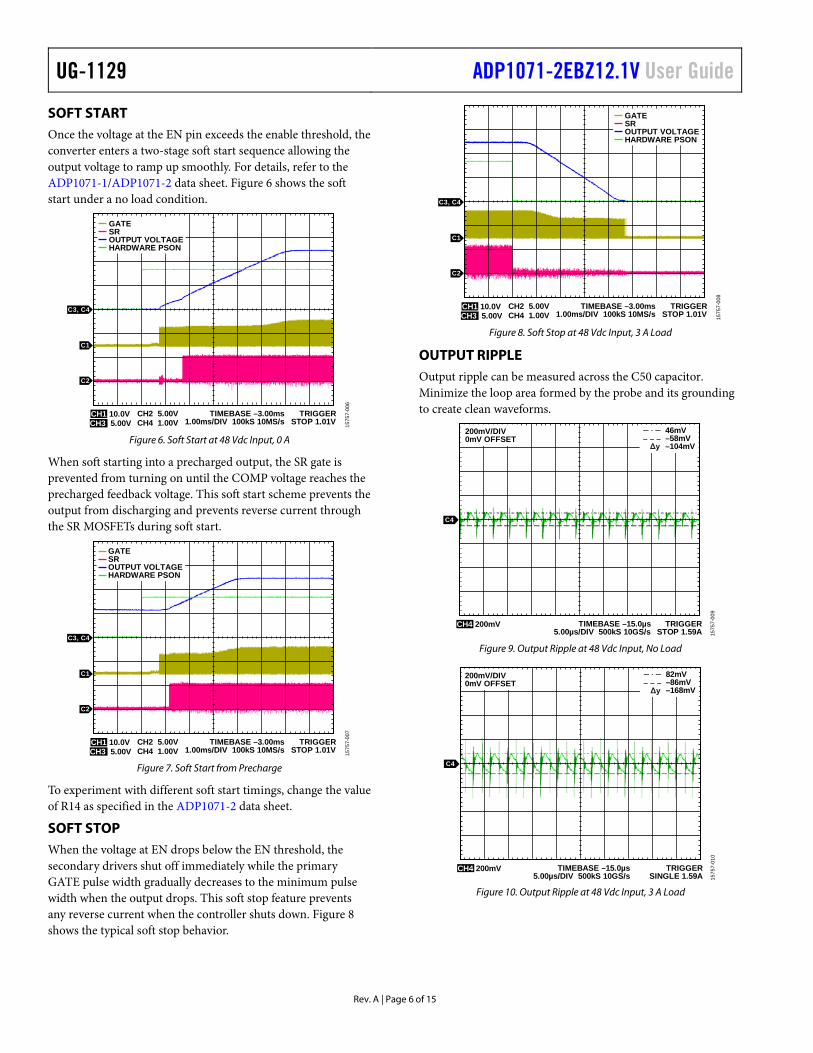
SOFT START Once the voltage at the EN pin exceeds the enable threshold, the converter enters a two-stage soft start sequence allowing the output voltage to ramp up smoothly. For details, refer to the ADP1071-1/ADP1071-2 data sheet. Figure 6 shows the soft start under a no load condition.
Figure 6. Soft Start at 48 Vdc Input, 0 A
When soft starting into a precharged output, the SR gate is prevented from turning on until the COMP voltage reaches the precharged feedback voltage. This soft start scheme prevents the output from discharging and prevents reverse current through the SR MOSFETs during soft start.
Figure 7. Soft Start from Precharge
To experiment with different soft start timings, change the value of R14 as specified in the ADP1071-2 data sheet.
SOFT STOP When the voltage at EN drops below the EN threshold, the secondary drivers shut off immediately while the primary GATE pulse width gradually decreases to the minimum pulse width when the output drops. This soft stop feature prevents any reverse current when the controller shuts down. Figure 8 shows the typical soft stop behavior.
Figure 8. Soft Stop at 48 Vdc Input, 3 A Load
OUTPUT RIPPLE Output ripple can be measured across the C50 capacitor. Minimize the loop area formed by the probe and its grounding to create clean waveforms.
Figure 9. Output Ripple at 48 Vdc Input, No Load
Figure 10. Output Ripple at 48 Vdc Input, 3 A Load
C3, C4
C2
C1
CH3 5.00VCH1 10.0V CH2 5.00V
CH4 1.00VTIMEBASE –3.00ms
1.00ms/DIV 100kS 10MS/sTRIGGER
STOP 1.01V
GATESROUTPUT VOLTAGEHARDWARE PSON
1575
7-00
6
C3, C4
C2
C1
CH3 5.00VCH1 10.0V CH2 5.00V
CH4 1.00VTIMEBASE –3.00ms
1.00ms/DIV 100kS 10MS/sTRIGGER
STOP 1.01V
GATESROUTPUT VOLTAGEHARDWARE PSON
1575
7-00
7
C3, C4
C2
C1
CH3 5.00VCH1 10.0V CH2 5.00V
CH4 1.00VTIMEBASE –3.00ms
1.00ms/DIV 100kS 10MS/sTRIGGER
STOP 1.01V
GATESROUTPUT VOLTAGEHARDWARE PSON
1575
7-00
8
C4
CH4 200mV TIMEBASE –15.0µs5.00µs/DIV 500kS 10GS/s
TRIGGERSTOP 1.59A
200mV/DIV0mV OFFSET
46mV–58mV–104mVΔy
1575
7-00
9
C4
CH4 200mV TIMEBASE –15.0µs5.00µs/DIV 500kS 10GS/s
TRIGGERSINGLE 1.59A
200mV/DIV0mV OFFSET
82mV–86mV–168mVΔy
1575
7-01
0

ADP1071-2EBZ12.1V User Guide UG-1129
Rev. A | Page 7 of 15
CONTROL LOOP On the secondary side, the output voltage information is sensed a voltage divider and sent to the FB pin. The FB pin voltage is compared to a 1.2 V reference signal, and the error determines the COMP voltage. The COMP pin voltage information is sent to the primary side via iCoupler technology, allowing closed loop operation.
The loop gain can be measured via a network analyzer. The small signal perturbation is injected at R19 and VOUT+ test points. Figure 11 shows the loop gain of the system.
Figure 11. Loop Gain Measurement
Transient Response for Load Step
A dynamic electronic load can be connected to the output of the evaluation board to evaluate the transient response. Set up an oscilloscope to capture the transient waveform of the power supply output. Figure 12 shows an example of the load transient response. Change the R18 resistor and C39 and C40 capacitors connected at the COMP pin to change the transient response.
Figure 12. Transient Response with Load Steps: 25% to 75% to 25%
EXTERNAL SIGNAL TRACKING The output voltage of the evaluation board can track an external signal applied to the SS2 pin. The applied peak value must be lower than 1.2 Vdc. Apply a 1 kHz, 200 mV peak-to-peak sinusoidal signal with 1.1 Vdc offset to SS2 in the example shown in Figure 13.
Figure 13. External Signal Tracking
61
100 1k 10k 100k
52
43
34
MA
GN
ITU
DE
(dB
)
PHA
SE (D
egre
es)
FREQUENCY (Hz)
25
16
7
–2
–11
–20
–29
130
110
90
70
50
30
10
–10
–30
–50
–70
1575
7-01
1
CROSSOVER FREQUENCY: 5.90kHzPHASE MARGIN: 68.87°GAIN MARGIN: 20.5dB
C3
C4
CH3 200mVCH4 200A
TIMEBASE –300µs100µs/DIV 100kS 100MS/s
TRIGGERSTOP 2.46A
AC COUPLED OUTPUT VOLTAGELOAD CURRENT 1A/µs
1575
7-01
2
C3
C1
CH1 500mVCH3 5.00V
TIMEBASE –1.50µs500µs/DIV 100kS 20MS/s
TRIGGERSTOP 1.090V
OUTPUT VOLTAGEINPUT SIGNAL
1575
7-01
3

UG-1129 ADP1071-2EBZ12.1V User Guide
Rev. A | Page 8 of 15
OVER CURRENT PROTECTION (OCP) The primary peak current is sensed by the cycle by cycle current sensing resistor, R15. When the sensed input peak current is above the CS pin limit threshold, the controller operates in the cycle by cycle constant current limit mode for 1.25 ms. The controller immediately shuts down the primary drivers and discharges the SS2 pin. The controller then goes into shutdown mode for the next 40 ms and restarts the soft start sequence. Figure 14 and Figure 15 show these protections features.
Figure 14. OCP Under Output Short Circuit at 48 Vdc
Figure 15. Recovery from Output Short Circuit at 48 Vdc
VOLTAGE AND CURRENT STRESS The drain to source voltage of both the main switch and SR MOSFET are clamped by the RCD snubber on the evaluation board. The peak drain to source voltage occurs at the maximum input voltage and full load. Figure 16 shows the peak drain to source voltages of the main switch and synchronous rectifier are 143.4 V and 45.3 V, respectively.
Figure 16. MOSFET Drain to Source Voltages at 60 Vdc Input and 5 A Load
(VDS means voltage from the drain source)
Peak current stress occurs at the minimum input voltage and full load, that is, at the 36 Vdc input and 5 A load (see Figure 17). The peak current is 5.43 A for the primary side. The rms value of the primary current under t condition is approximately 2.67 A.
Figure 17. Peak Primary Current at 36 Vdc Input and 5 A Load
C1
C2
C4
C3
CH1 20.0V CH2 10.0VCH4 10.0ACH3 5.00V
TIMEBASE 0ms50.0ms/DIV 100kS 200kS/s
TRIGGERSTOP 7.00V
GATESROUTPUT VOLTAGEOUTPUT CURRENT
1575
7-01
4
C4
C3
C1
C2
CH1 20.0V CH2 10.0VCH4 10.0ACH3 5.00V
TIMEBASE 0ms50.0ms/DIV 100kS 200kS/s
TRIGGERSTOP 6.20V
GATESROUTPUT VOLTAGEOUTPUT CURRENT
1575
7-01
5
C4
C1 C2
TIMEBASE –15.0µs500ns/DIV 25.0kS 5.0GS/s
TRIGGERSTOP 62.5V
CH1 50.0V CH2 20.0VCH4 5.00A
VDS OF MAIN SWITCHVDS OF SRPRIMARY CURRENT
1575
7-01
6
C1 C2
C4
TIMEBASE –15.0µs5.00ns/DIV 25.0kS 5.0GS/s
TRIGGERSTOP 62.5V
CH1 50.0V CH2 20.0VCH4 5.00A
GATESRPRIMARY CURRENT
1575
7-01
7

ADP1071-2EBZ12.1V User Guide UG-1129
Rev. A | Page 9 of 15
EFFICIENCY CURVES Figure 18 and Figure 19 show the typical efficiency curves under line and load conditions, respectively.
Figure 18. Efficiency Curves
Figure 19. Load Regulation
THERMAL PERFORMANCE Figure 20 show the typical thermal profile of the evaluation board at different operating conditions.
Figure 20. Thermal Image of the ADP1071-2 at 48 Vdc Input, 5 A Load, No
Airflow, and 0.5 Hour Soaking Time
95
90
85
80
75
EFFI
CIE
NC
Y (%
)
70
65
60
555.04.54.03.53.02.5
OUTPUT CURRENT (A)2.01.51.00.5
36V48V60V
1575
7-01
8
12.5
12.4
OU
TPU
T VO
LTA
GE
(V)
12.3
12.2
12.1
12.03
LOAD CURRENT (A)210
1575
7-01
9
1575
7-02
0

UG-1129 ADP1071-2EBZ12.1V User Guide
Rev. A | Page 10 of 15
EVALUATION BOARD SCHEMATIC AND ARTWORK
Figure 21. ADP1071-2EBZ12.1V Evaluation Board Schematic
J3
12
C46
DN
I
R40
DN
I
R41
DN
I
D5
BZT
52C
11-7
-F
AC
SYN
C
TP17
PGN
D1
VOU
T
TP18
AG
ND
1
MB
R2H
200S
FT1G
D9
AC
C28
68uF
MB
R2H
200S
FT1G
D16
AC
VIN
MB
R2H
200S
FT1G
D17
A C
MB
R2H
200S
FT1G
D18
AC
MB
R2H
200S
FT1G D19
AC
R27
80.6
K
CO
MP
C40
2nF
R18
24.9
k
1%
1%1%
C39
100p
F
+C
23
150u
F
P N
+C
5015
0uF
P N
VIN
+ VIN
+
VIN
- VIN
-
R29
0
MB
R2H
200S
FT1G
D20
AC
SS2
RT
C36
0.1u
F
C51
100p
F
CO
MP
C6
22uF
2KV
C32
C38
2.2u
F
GA
TE
C41
0.1u
F
T1 PA17
36N
L
9 1012
6 1 2 4 3
8 11
5
7
R15
15m
R
C2
470p
F
R14
10k
R2
48.7
R12
2.2k
VDD
2
EMK
316B
B72
26M
L-T
C48
2.2u
F
SR
C1
2.2u
F
C42
1uF
R16 0
C27
2.2u
F
R42
10k
C26
2.2u
F
J2
VIN
+
1
TP8 PG
ND
2TP9
R34
10k
ERJ-
8GEY
J103
V
VAU
X1
AG
ND
1
CS
J6
1
2
345
R49
33k
EN
VREG
2
C35
DN
I
R20
8.87
kR
230.
976k
R21
8.87
k
R24
1k
R19 10
VOU
TVO
UT
TP10
FBO
VP
Q8 4
5
3
2 1
Q2
BSC
0904
NSI
4
PAD
3
2 1
VREG
2
FBOVP
SS2
VIN
_IC EN
U1
AD
P107
1-2
GA
TE1
AG
ND
12
VREG
13
VIN
4
EN5
SYN
C8
CS
6
RT
7
SS2
9
CO
MP
10
FB11
OVP
12
VDD
213
VREG
214
AG
ND
215
SR16
VREG
1
GA
TE
AG
ND
1 RT
SYN
CCS
CO
MP
VOU
T
VDD
2
C29
10nF
R3
10k
C25
2.2u
FC
242.
2uF
DN
I
D13
A C
US1
D
D11
AC
J8
1
2
345
OVP
SR
J9
1
2
34
5
SS2
J1 VOU
T+
1
SR
J5 VOU
T-
1
D12 DN
I
A C
VREG
1
R1
DN
I
VREG
1
J4
VIN
-
1
VIN
_IC
R35
33k
10
R39
10K
R38
10K
VREG
R17 33
k
C20DN
I
C22
22uF
C21DN
I
Q7
FMB
S238
3
C14
22uF
C4
DN
I
C15DN
I
C16DN
I
C5
22uF
C17DN
I
C18
22uF
C19
22uF
VIN
SS2
SW1
21
3
R10 4.
7
Q6
FMB
S238
3
SYN
C
R37
100
D14
BZT
52C
8V2
AC
FB
D10
BZT
52C
13-7
-FA
C
R32 0R
33
DN
IVR
EG1
GA
TE
R28
135k
R31
4.75
k
R9 0
TP4
C37
2.2u
F
Q3
FDM
S862
004
5
876 3
2
1
VIN
_IC
C33
22nF
R7
10kC31
0.1u
F
VIN
VOU
TVO
UT+
TP5
VOU
T-
1%
15757-021
2200
pF C
4532
X7R
3D22
2K13
0KA

ADP1071-2EBZ12.1V User Guide UG-1129
Rev. A | Page 11 of 15
Figure 22. Board Outline
Figure 23. Silkscreen Top
Figure 24. Silkscreen Bottom
1575
7-02
215
757-
023
1575
7-02
4

UG-1129 ADP1071-2EBZ12.1V User Guide
Rev. A | Page 12 of 15
Figure 25. PCB Layout, Top Layer
Figure 26. PCB Layout, Layer 2
Figure 27. PCB Layout, Layer 3
1575
7-02
515
757-
026
1575
7-02
7

ADP1071-2EBZ12.1V User Guide UG-1129
Rev. A | Page 13 of 15
Figure 28. PCB Layout, Layer 4
1575
7-02
8

UG-1129 ADP1071-2EBZ12.1V User Guide
Rev. A | Page 14 of 15
ORDERING INFORMATION BILL OF MATERIALS
Table 3. Reference Designator Description Manufacture Part Number C1, C37, C38, C48 Ceramic capacitors, 2.2 μF, 50 V, 10%, X7R, surface mount device (SMD) Murata GRM188R61H225KE11D C2 Ceramic capacitor, 470 pF, 100 V, 10%, X7R, SMD Murata GRM188R72A471KA01D C5, C6, C14, C18, C19, C22
Ceramic capacitors, 47 μF, 16 V, X5R Taiyo Yuden C3216X5R1C476M160AB
C4, C15 to C17, C21, C20
Do not install (DNI)
C23, C50 Tantalum polymer capacitors, 150 μF, 16 V Panasonic 1CTQC15173F1 C24 to C27 Ceramic capacitors, 2.2 μF, 100 V, 10%, X7R, SMD AVX Corporation 12101C225KAT2A C28 Aluminum capacitor, 100 V, 68 μF, 20% Panasonic EEV-FK2A680Q C29 Ceramic capacitors, 10 nF, 200 V, 10%, X7R, SMD AVX 12062C103KAT2A C31 Ceramic capacitor, 0.1 μF, 200 V, X7R, 1206 Murata C1206C104K2RACTU C32 Ceramic capacitor, 2200 pF, 2 kV, X7R, 1812 TDK C4532X7R3D222K130KA C33 Ceramic capacitor, 0.022 μF (22 nF), 250 V, X7R, 1206 TDK C3216X7R2E223K115AA C46 Ceramic capacitor, 0.022 μF, 250 V, X7R, 1206, DNI TDK C3216X7R2E223K115AA C35 Ceramic capacitor, 100 pF, 50 V, 10%, X7R, DNI, SMD Kemet or equivalent C0603C101K5RACTU C39, C51 Ceramic capacitors, 100 pF, 50V, 10%, X7R SMD Kemet or equivalent C0603C101K5RACTU C36, C41 Ceramic capacitors, 0.1 μF, 25 V, 10%, X7R, SMD AVX Corporation 06033C104KAT2A C40 Ceramic capacitor, 2000 pF (2 nF), 100 V, 10%, X7R, SMD AVX Corporation 06031C202KAT2A C42, C43 Ceramic capacitors, 1 μF, 50 V, X7R, 0603 T-Y UMK107AB7105KA D10, D5, D14 Zenner diodes, 11 V, 500 mW, 5%, BZT52C11-7-F Diode Inc. BZT52C11-7-F D11 Ultrafast diode, 200 V, 1 A MMC US1D D13 Ultrafast diode, 200 V, 1 A, DNI MMC US1D D12 Transient voltage suppression Zenner diode, 40 V, DNI Littlefuse 5.0SMDJ36 D9, D16 to D19 Ultrafast diodes, 200 V, 1A ON Semiconductor MBR2H200SFT1G J1 Banana jack connector, VOUT+ Emerson 108-0740-001 J2 Banana jack connector, VIN+ Emerson 108-0740-001 J3 Jumper J4 Banana jack connector, VIN− Emerson 108-0740-001 J5 Banana jack connector, VOUT− Emerson 108-0740-001 J6, J8, J9 Jack connectors, vertical gold, DNI Emerson 131-3701-261 Q2 N-channel power trench, 60 V, 46 A, 9.7 mΩ Infineon BSC097N06 Q3 N-channel power trench,150 V, 35 A, 18 mΩ Fairchild FDMS86200 Q6, Q7 NPN transistors, 160 V, 0.8 A Fairchild FMBS2383 R1 SMD resistor, DNI, 1/8 W, jumper Panasonic ERJ-6GEY0R00V R2 SMD resistor, 48.7 Ω, 1/8 W, 1% Vishay/Dale CRCW080548R7FKEA R3, R34, R38, R39 SMD resistors, 10 kΩ, 0.25 W, 5%, 1206 Panasonic ERJ-8GEYJ103V R7, R14 SMD resistor, 10 kΩ, 1/8 W, 1% Any R9 SMD resistor, 0 Ω, 1/8 W, jumper Any R10 SMD resistor, 4.7 Ω, 1/8 W Any R12 SMD resistor, 2.2 kΩ, 1/8 W, 1% Any R15 Current sense resistor 15 mΩ, 1 W, 1% Panasonic ERJ-8BWFR015V R16, R29, R32 SMD resistors, 0 Ω, 1/8 W, jumper Any R17, R35, R49 SMD resistors, 33 kΩ,1/8 W, 1% Any R18 SMD resistor, 24.9 kΩ, 1/8 W 1% Any R19 SMD resistor, 10 Ω, 1/10 W Any R20, R21 SMD resistors, 8.87 kΩ, 1/8 W, 1% Any R33 SMD resistor, DNI, 1/8 W, jumper Any R23, R24 SMD resistors, 0.976 kΩ, 1/8 W, 1% Any

ADP1071-2EBZ12.1V User Guide UG-1129
Rev. A | Page 15 of 15
Reference Designator Description Manufacture Part Number R27 SMD resistor, 80.6 kΩ, 1/8 W, 1% Any R28 SMD resistor, 133 kΩ, 1/5 W, 0.1% Any R31 SMD resistor, 4.75 kΩ, 1/8 W, 1% Any R36, R37 SMD resistors, 100 Ω, 1/8 W, 1% Any R40, R41 DNI Any R42 SMD resistor, 10 kΩ, 1/8 W, 1% Any SW1 Switch slide, single-pole, double-throw, 30 V, 0.2 A E-Switch EG1218 TP1 to TP7, TP10, TP13 to TP16, TP18, TP19
PC test points, mini SMD Keystone 5019
TP8 PC test point, mini SMD, PGND2 Keystone 5019 TP9 PC test point, mini SMD, GND Keystone 5019 TP17 PC test point, mini SMD, PGND1 Keystone 5019 T1 Transformer Pulse PA1736NL U1 Isolated controller Analog Devices ADP1071-2
ESD Caution ESD (electrostatic discharge) sensitive device. Charged devices and circuit boards can discharge without detection. Although this product features patented or proprietary protection circuitry, damage may occur on devices subjected to high energy ESD. Therefore, proper ESD precautions should be taken to avoid performance degradation or loss of functionality.
Legal Terms and Conditions By using the evaluation board discussed herein (together with any tools, components documentation or support materials, the “Evaluation Board”), you are agreeing to be bound by the terms and conditions set forth below (“Agreement”) unless you have purchased the Evaluation Board, in which case the Analog Devices Standard Terms and Conditions of Sale shall govern. Do not use the Evaluation Board until you have read and agreed to the Agreement. Your use of the Evaluation Board shall signify your acceptance of the Agreement. This Agreement is made by and between you (“Customer”) and Analog Devices, Inc. (“ADI”), with its principal place of business at One Technology Way, Norwood, MA 02062, USA. Subject to the terms and conditions of the Agreement, ADI hereby grants to Customer a free, limited, personal, temporary, non-exclusive, non-sublicensable, non-transferable license to use the Evaluation Board FOR EVALUATION PURPOSES ONLY. Customer understands and agrees that the Evaluation Board is provided for the sole and exclusive purpose referenced above, and agrees not to use the Evaluation Board for any other purpose. Furthermore, the license granted is expressly made subject to the following additional limitations: Customer shall not (i) rent, lease, display, sell, transfer, assign, sublicense, or distribute the Evaluation Board; and (ii) permit any Third Party to access the Evaluation Board. As used herein, the term “Third Party” includes any entity other than ADI, Customer, their employees, affiliates and in-house consultants. The Evaluation Board is NOT sold to Customer; all rights not expressly granted herein, including ownership of the Evaluation Board, are reserved by ADI. CONFIDENTIALITY. This Agreement and the Evaluation Board shall all be considered the confidential and proprietary information of ADI. Customer may not disclose or transfer any portion of the Evaluation Board to any other party for any reason. Upon discontinuation of use of the Evaluation Board or termination of this Agreement, Customer agrees to promptly return the Evaluation Board to ADI. ADDITIONAL RESTRICTIONS. Customer may not disassemble, decompile or reverse engineer chips on the Evaluation Board. Customer shall inform ADI of any occurred damages or any modifications or alterations it makes to the Evaluation Board, including but not limited to soldering or any other activity that affects the material content of the Evaluation Board. Modifications to the Evaluation Board must comply with applicable law, including but not limited to the RoHS Directive. TERMINATION. ADI may terminate this Agreement at any time upon giving written notice to Customer. Customer agrees to return to ADI the Evaluation Board at that time. LIMITATION OF LIABILITY. THE EVALUATION BOARD PROVIDED HEREUNDER IS PROVIDED “AS IS” AND ADI MAKES NO WARRANTIES OR REPRESENTATIONS OF ANY KIND WITH RESPECT TO IT. ADI SPECIFICALLY DISCLAIMS ANY REPRESENTATIONS, ENDORSEMENTS, GUARANTEES, OR WARRANTIES, EXPRESS OR IMPLIED, RELATED TO THE EVALUATION BOARD INCLUDING, BUT NOT LIMITED TO, THE IMPLIED WARRANTY OF MERCHANTABILITY, TITLE, FITNESS FOR A PARTICULAR PURPOSE OR NONINFRINGEMENT OF INTELLECTUAL PROPERTY RIGHTS. IN NO EVENT WILL ADI AND ITS LICENSORS BE LIABLE FOR ANY INCIDENTAL, SPECIAL, INDIRECT, OR CONSEQUENTIAL DAMAGES RESULTING FROM CUSTOMER’S POSSESSION OR USE OF THE EVALUATION BOARD, INCLUDING BUT NOT LIMITED TO LOST PROFITS, DELAY COSTS, LABOR COSTS OR LOSS OF GOODWILL. ADI’S TOTAL LIABILITY FROM ANY AND ALL CAUSES SHALL BE LIMITED TO THE AMOUNT OF ONE HUNDRED US DOLLARS ($100.00). EXPORT. Customer agrees that it will not directly or indirectly export the Evaluation Board to another country, and that it will comply with all applicable United States federal laws and regulations relating to exports. GOVERNING LAW. This Agreement shall be governed by and construed in accordance with the substantive laws of the Commonwealth of Massachusetts (excluding conflict of law rules). Any legal action regarding this Agreement will be heard in the state or federal courts having jurisdiction in Suffolk County, Massachusetts, and Customer hereby submits to the personal jurisdiction and venue of such courts. The United Nations Convention on Contracts for the International Sale of Goods shall not apply to this Agreement and is expressly disclaimed.
©2018 Analog Devices, Inc. All rights reserved. Trademarks and registered trademarks are the property of their respective owners. UG15757-0-12/18(A)