Embed Size (px)
Citation preview

ADP1048 600 Watt Evaluation Kit
ADP1048-600-EVALZ PRD 1363
Rev. 1.3 Reference designs are as supplied “as is” and without warranties of any kind, express, implied, or statutory including, but not limited to, any implied warranty of merchantability or fitness for a particular purpose. No license is granted by implication or otherwise under any patents or other intellectual property by application or use of reference designs. Information furnished by Analog Devices is believed to be accurate and reliable. However, no responsibility is assumed by Analog Devices for its use, nor for any infringements of patents or other rights of third parties that may result from its use. Analog Devices reserves the right to change devices or specifications at any time without notice. Trademarks and registered trademarks are the property of their respective owners. Reference designs are not authorized to be used in life support devices or systems.
One Technology Way, P.O. Box 9106, Norwood, MA 02062-9106, U.S.A.Tel: 781.329.4700 www.analog.com Fax: 781.461.3113 ©2009 Analog Devices, Inc. All rights reserved.
FEATURES Interleaved Boost PFC topology providing high power factor and low THD Protection features for AC line input and high voltage output Current balancing between two phases High efficiency I2C serial interface to PC Software GUI Programmable digital filters Programmable response to faults Programmable inrush control Accurate AC power metering Digital Calibration and trimming
CAUTION This evaluation board uses high voltages whenever it is powered up. The output capacitor has high level of energy stored and it must be discharged before the load is disconnected. Extreme caution must be taken to ensure safety for the user. It is strongly advised to power down the evaluation board when not in use.
ADP1048 EVALUATION BOARD OVERVIEW This evaluation board features the ADP1048 in a switching power supply application. With the evaluation board and software, the ADP1048 can be interfaced to any PC running Windows 2000/XP/Vista/NT via the computer's USB port. The software allows control and monitoring of the ADP1048 internal registers. The board is set up for the ADP1048 to act as boost power factor correction circuit with a rated load of 600W from an input voltage ranging from a 85 VRMS to 265 VRMS.
EVALUATION SYSTEM CONTENTS The evaluation system package contains the following items: • Application note EVAL-ADP1048 (order code: ADP1048-600-EVALZ) • ADP1048 evaluation board The USB/I2C adapter for serial communication and software CD need to be ordered separately.

ADP1048-600-EVALZ PRD 1363
Rev. 1.3 | Page 2 of 26
TABLE OF CONTENTS Features ....................................................................................................................................................................................... 1
CAUTION ..................................................................................................................................................................................... 1
TOPOLOGY AND circuit description ............................................................................................................................................ 3
CONNECTORS ............................................................................................................................................................................ 3
SETTING FILES AND EEPROM .............................................................................................................................................. 5
BOARD EVALUATION ................................................................................................................................................................. 6
EQUIPMENT ............................................................................................................................................................................ 6
SETUP ...................................................................................................................................................................................... 8
ADP1048 PROGRAMMING SOFTWARE .............................................................................................................................. 10
APPENDIX I – SCHEMATIC (MAIN BOARD) ............................................................................................................................ 11
APPENDIX II – SCHEMATIC (DAUGHTER CARD) ................................................................................................................... 14
APPENDIX III – LAYOUT (MAIN BOARD) ................................................................................................................................. 15
APPENDIX IV – LAYOUT (DAUGHTER CARD) ........................................................................................................................ 17
APPENDIX X – BILL OF MATERIALS (MAIN BOARD) .............................................................................................................. 20
APPENDIX XI – BILL OF MATERIALS (DAUGHTER CARD) .................................................................................................... 23
APPENDIX XII – REGISTER FILE (RevA_IC revised-0408.48r) ............................................................................................... 24
Notes .......................................................................................................................................................................................... 26
DEMO BOARD SPECIFICATIONS
Specification MIN TYP MAX Units Notes
VIN 85 115 or 230 265 VRMS
VOUT 385 V
POUT 0.0 600 W
TAMBIENT 0 30 65 ºC
Efficiency 95 %
Switching frequency 97.7 KHz
Table 1 - Target Specifications

ADP1048-600-EVALZ PRD 1363
Rev. 1.3 | Page 3 of 26
TOPOLOGY AND CIRCUIT DESCRIPTION This evaluation board features the ADP1048 in a typical AC/DC switching power supply in an interleaved boost power factor correction (PFC) topology. The circuit is designed to provide a rated load of 385V/600W from an AC input voltage source of 85 VRMS to 265 VRMS AC. The ADP1048 provides functions all the functions necessary for active PFC circuit plus accurate AC power metering. It achieves near-unity power factor, low distortion of the input current, the output voltage regulation, over current protection, AC line fault detection and protection, over temperature protection, and power supply shutdown. It also can optimize light load efficiency performance using output voltage adjustment and frequency reduction.
Please refer to the appendix for the detailed schematic. The AC input side consists of the input terminals, EMI filter, inrush relay and its control circuit. The D1 is the rectifier bridge for main power transmission. The D4 is used for input voltage sensing. The boost circuit consists boost inductor (L2), boost switch (Q1) and diode (D2). The gate signal for the boost switch comes from the ADP1048 through the ADP3634 gate driver. The ADP1048 (U1, on daughter card) can be powered either via the USB 5V via an ADP3303 LDO (U2, on daughter card) present on the same daughter card, or via the auxiliary power supply on the board. Thermistor (RTD1) is placed close to the MOSFET on the board allowing over temperature protection functionality to be implemented.
CONNECTORS The connections to the evaluation board are shown below.
Connector Evaluation Board Function
J1 AC Input
J9, J10 AC Input
J4 385V DC Voltage Output
J5 Ground Return for 385 V DC Voltage
Output
J8, J11 I2C Connector
J6 Daughter card
Table 2 - Evaluation board connectors
There is a 4 pin connector for I2C communication. This allows the software to communicate with the evaluation board through the USB port of the PC. Connectors (J8 and J11) are identical and are connected in parallel to each other to allow multiple boards to be connected to the same I2C bus in a daisy chain configuration.

ADP1048-600-EVALZ PRD 1363
Rev. 1.3 | Page 4 of 26
Figure 1 - Evaluation Board Setup
Pin Evaluation Board Function
1 5V
2 SCL
3 SDA
4 Ground
Table 3 - J8, J11 connections
AC Power Meter
DC V Multi Meter
AardvarkPC
ELECTRONICLOADAC POWER
SUPPLY
J10
J9
SW1
J4
J5TP26
TP5
COM1-J8 (orJ11)
HILO
IHILO
I
COM
+
-
A
(or J1)
Vout
Figure 2 - Test configuration for the Evaluation Board

ADP1048-600-EVALZ PRD 1363
Rev. 1.3 | Page 5 of 26
SETTING FILES AND EEPROM The ADP1048 communicates with the GUI software using the I2C bus.
DigitalBlock
I2CRAMEEPROMUSB to I2CInterfaceAdapter
ADP1048 GUI
Board SetupFile
RegisterSettings File
Figure 3 - ADP1048 and GUI interaction
The register settings (having extension .48r) and the board settings (having extension .48b) are two files that are associated with the ADP1048 software. The register settings file contains information that govern the functionality of the part such as the over voltage and over current limits, softstart timing, PWM settings etc. The ADP1048 stores all its settings in the EEPROM. When the ADP1048 is connected to the USB adapter the LDO powers the I.C. and the GUI downloads the settings from the registers of the ADP1048 so that the state of the part is known. It is possible to save these settings in a file for later use. Older register settings are overwritten when new files are loaded.
The EEPROM on the ADP1048 can contain the information about the board, such as current sense resistor, output inductor and capacitor values. This information is also stored in board setup file (extension .48b) and is necessary for the GUI to display the correct information in the ‘Monitor’ tab as well as ‘Filter Settings’ window. Always make sure that the correct board file has been loaded for the board currently in use.
Each ADP1048 chip has trim registers for the temperature, input current and the output voltage and input voltage. These can be configured during production and are not overwritten whenever a new register settings file is loaded. This is done in order to retain the trimming of all the ADCs for that corresponding environmental and circuit condition (component tolerances, thermal drift, etc.).

ADP1048-600-EVALZ PRD 1363
Rev. 1.3 | Page 6 of 26
BOARD EVALUATION
EQUIPMENT • AC Power Supply
• Electronic Load
• Oscilloscope with differential probes
• PC with ADP1048 GUI installed
• Precision Digital Multimeters (HP34401or equivalent - 6 digits) for measuring DC current and voltage
Figure 4 - 600W evaluation board showing PS_ON hardware switch
PS_ON

ADP1048-600-EVALZ PRD 1363
Rev. 1.3 | Page 7 of 26
Figure 5 - ADP1048 daughter card

ADP1048-600-EVALZ PRD 1363
Rev. 1.3 | Page 8 of 26
SETUP NOTE: DO NOT CONNECT THE USB CABLE TO THE EVALUATION BOARD UNTIL THE SOFTWARE HAS FINISHED INSTALLING
1) Install the ADP1048 software by inserting the installation CD. The software setup will start automatically and a guided process will install the software as well as the USB drivers for communication of the GUI with the IC using the USB adapter.
2) Insert the daughter card in connector J6 as shown in Figure 4.
3) Ensure that the PS_ON switch (SW1 on schematic) is turned to the on position. It is located on the bottom left half of the board (Figure 4).
4) Connect the evaluation board to the USB port on the PC using the “USB to I2C interface” adapter as shown in Figure 1.
5) The software should report that the ADP1048 has been located on the board. Click “Finish” to proceed to the Main Software Interface Window. The serial number reported on the side of the checkbox indicates the USB adapter serial number. The windows also displays the device I2C address.
Figure 6 - ADP1048 address in the GUI
6) If the software does not detect the part it enters into simulation mode. Ensure that the connector is connected to J8/J11 (on main board) Click on ‘Scan for ADP1048A now’ icon (magnifying glass) located on the top right hand corner of the screen.
Figure 7 - “Scan for ADP1048 Now’ icon
7) The board setting is store in the IC and this step is optional. Click on the “Load Board Settings” icon (fourth button from the left) and select the ADI default.48b file. This file contains all the board information including values of shunt and voltage dividers. Note: All board setting files have an extension of .48b
Figure 8 - Different icons on dashboard for loading and saving .48r and .48b files
8) The IC on the evaluation board comes preprogrammed and this step is optional. The original register configuration is stored in the ADP1048.48r register file. Note: All register files have an extension of .48r. The file can be loaded using the second icon from the left in Figure .

ADP1048-600-EVALZ PRD 1363
Rev. 1.3 | Page 9 of 26
9) Connect a resistive or electronic load to the output connections of Vout+ and Vout-. Note that the load should be connected before the input power is supplied to the evaluation board for safety concerns.
10) Connect a 50 or 60 Hz ac power source, which has to be turned off, to ac plug J1 or terminals J9 and J10.
11) Turn on AC power source and increase the input voltage within the range from 85Vrms to 265Vrms.
12) The evaluation board should now up and running, and ready for evaluation. The output should now read about 385 VDC.
13) Click on the ‘MONITOR’ tab and then on the Flags and readings icon. This window provides a snapshot of the entire state of the PSU in a single user friendly window.
Figure 9 - Monitor window in GUI
During power up, the ADP1048 is connected to the USB port (5V) and the LDO powers the IC. It takes 20µsec for VCORE (pin 26) to reach an internal voltage of 2.5V. After this, the I.C. downloads the contents of the registers into the EEPROM. After this the softstart ramp begins.
After successful startup and in steady state condition, 5 LEDs on the board to provide to the user the status of the board. All the LEDs will be turned ON indicating that there are no faults detected such as over voltage or over current. In case of a fault the PGOOD or AC_OK LEDs will be turned OFF indicating that some flag has tripped due to an out of bounds condition. The monitor window will display the appropriate state of the PSU.
LED Location Description
D7 Bottom left Inrush signal
D8 Bottom right PGOOD signal (active high)
D9 Bottom right AC_OK signal (active high)
D10 Bottom right Indicates input voltage is present
D11 Top right Indicates 12V or USB5V is present
Table 4 – List of LEDs on the evaluation board

ADP1048-600-EVALZ PRD 1363
Rev. 1.3 | Page 10 of 26
ADP1048 PROGRAMMING SOFTWARE The goal of this evaluation kit is to allow the user to get an insight into the flexibility offered by the extensive programming options offered by the ADP1048. Several test points on the board allow easy monitoring of the various signals. The user can also use the software to program multiple responses (such as disable power supply or disable the PWM) for various fault conditions. There are several main windows where the user can use to program and evaluate the PSU. They can be accessed from the Setup window in the GUI. The ADP1048 can be easily programmed to modify the behavior of the PSU under different fault and load conditions without any hardware changes. All the changes are purely through software and do not require desoldering components and replacing them with new values to specify a different operating condition

ADP1048-600-EVALZ PRD 1363
Rev. 1.3 | Page 11 of 26
APPENDIX I – SCHEMATIC (MAIN BOARD)
R1
24
99k
TP
22G
ate
2
PG
ND
OV
P
Vou
t
100V
AC
-RE
CR
21
49
9k
R2
64
99k
R5
010
Gat
e_Q
1
TP
19V
out-
TP
12A
C_
RE
C_
Se
nse
100V
R8
10
Vou
t
PG
ND
R1
447
0k,
1W
R3
34
99k
PG
ND
VC
C+1
2V
TP1
5V
AC
TP
5V
out
+
C2
0.47
u, 2
50V
R3
7D
NP
1kV
TP1
6P
GN
D
+-
~ ~
D4
MB
6S
~11
+3
~22
-4
J9 P1
TP
20O
VP
R4
.08
OH
M ,
2W
C1
41
00pF
C4
DN
P
PW
M2
AC
-RE
C_
sen
se
R3
14
99k
R39
1k
PG
ND
R4
024
9k
TP1
7V
in1
REDUNDANT OVP
Th OFF=1.28V -> 500V
Th ON= 1.0V ->390V
R40=390k
R39=1k
D1
58
ET
X06
21
TP3
AC
-RE
C+
AC
-RE
C_s
ens
e
1kV
TP
25
PG
ND
PG
ND
C7
330
u, 4
50V
R27
10k
1N
414
8D
5
AC
R5
390,
1W
R1
84
99k
OTW
C20
1n
C8
DN
P
TP1
3V
BU
S
R1
94
99k
L3
500U
TP1
4P
GN
D
PW
M
K1
G6
RL-
1A-D
C1
22
31 4
C1
10
.33u
, 63
0V
R42
10
J4
VO
UT
+1
R4
314
0k
TP
10+
12
D7
LE
D
R2
225
Oh
m
TP
26V
out
-
VC
C+1
2V
R15
0
INR
US
H
R2
32
k2
Q2
SP
W2
0N
60
C3
1
2 3
PG
ND
TP2
7V
ou
t-
Vou
t
F1
8A
Vo
ut
R4
1D
NP
RED
U1
AD
P3
634
EN
#1
INA
2
GN
D3
INB
4
OTW
8
OU
TA
7V
DD
6O
UT
B5
R29
10k
J16
12
RED
J17
12
VF
B
R2
82
5m
3W
TP2
8P
GN
D
TP
8C
S-
TP
1A
C-I
N+
C12
0.1u
CS
+
+-
~ ~D
1G
BU
806
~12
+4
~23
-1
TP
11C
S+
L2
500U
TP
7A
C-R
EC
-
TP1
8V
in2
R6
0
TP
9P
WM
C15
10
0pF
1N4
148
D1
6
AC
Q3
2SK
301
81
3 2
Q1
SP
W20
N60
C3
1
2 3R
34
36.5
k
R3
47
0k,
1W
TP
24
PW
M2
C6
0.3
3u,
630V
D3
8E
WS
08S
231
J5
VO
UT
-1
J18
12
J10 N
1
Gat
e_Q
2
C1
61
n
C30
68p
F
J14
12
TP2
9P
GN
D
PG
ND
IBA
L
AC
-RE
C
R1
33
6.5
k
R7
DN
P
VA
C
C10
4.7u
PG
ND
C1
0.47
u, 2
50V
D2
8E
TX
06
21
R2
03
6.5
k
C1
3
22u
TP
21In
rus
h
AC
-RE
C
R1
47
0k,
1W
R5
1
.08
OH
M ,
2W
STAR CONNE
CTION POINT
C3
DN
P
Ga
te_
Q1
TP2
AC
-IN
-
ILIM
25V
J12
12
J1 AC
Plu
g
11
22
33
J13
JUM
PE
R
L1 1.9m
H
1 2
4 3
R9 0
PG
ND
CS
-
Ga
te_
Q2
C9
0.1
u
PG
ND
C5
68
pF
R1
00
TP
4G
ate
R30
390
, 1
W
R2
10k
C21
330u
, 45
0V
D1
0LE
D
PG
ND
J15
12
TP
6V
x
R1
14
99k
TP2
3V
x2

ADP1048-600-EVALZ PRD 1363
Rev. 1.3 | Page 12 of 26
PGND
J7
11
22
J11
11
22
33
44
J6ADP1047_DC
CS+8CS-7PGND16INRUSH5NC34NC23NC12VAC1
AC_OK16PGOOD15PGND414ILIM13PGND312
PGND210PWM9
PWM211
SYNC17
NC418
12V/5V19
PGND520
NC521
PGND622
IBAL23
PGND724
RTD25
SDA26
SCL27
3.3V28
PSON29
AGND30
VFB31
OVP32
Input Voltage Sensing
Control Signal
VCC+12V
AC_OK
Inductor Current Sensing (-)Inductor Current Sensing (+)
PFC Gate
PGND
PGND
C1833pF
C1933pF
R45100
C2233pF
R49100
C2933pF
SCL
SDA
PFC Gate #2 (1048 Only)
PGOOD
Current Limiting
Power Good FlagAC OK Flag
RTD133k
RTD
PGND
Synchronization Signal
RTD
+12V
I Balancing Signal (1048 Only)
Temperature
Bulk Voltage
CS+
Over Voltage Protection
+5V
ILIM
AC_OK
OVP
PGND
TP30PSON
+3.3V
SW1
21
3
D11LED
D8LED
+5V
PGND
D9LED
PGND
VAC
GREENGREENPWM2
CS-
VFB
INRUSH
PWM
R242k2
PGOOD
SYNC
VCC+12V
IBAL
R252k2
1N4148D13
AC
RED
+3.3V
1N4148D17
AC
J8
11
22
33
44
C171nF
PGND
R32 2k2
PGND
SDASCL

ADP1048-600-EVALZ PRD 1363
Rev. 1.3 | Page 13 of 26
V2+
V2-
C26470pF
PGND
Vout
J211 2
C231nF
R16470K
200V
1000V
J22
11
22
D12DL4007
PGND
200V
200V
D18US1D
PGND
C28100uF
200V
R355.1K
50V 25V
R3647 Ohm
1000V
1000V
25V
VCC+12VR475.1K
C24470pF
D14US1D
C25100uF
R467.96K
R17300 Ohm
R3848.2K
C271uF
T4EE13
5
1
8
7
6
4
3
2 9
10
R4447 Ohm
U5LNK606
BP/M2S2
6
S1
5
S37
S48
D4
FB1NC
3
D6DL4007
R485.1K

ADP1048-600-EVALZ PRD 1363
Rev. 1.3 | Page 14 of 26
APPENDIX II – SCHEMATIC (DAUGHTER CARD)
PG
OO
D
C1
00
.1uF
C16
10pF
5V
1N
414
8D
2
21
R2
10k
INR
US
H
PG
ND
SY
NC
DG
ND
SC
L
SD
A
AG
ND
12V
1N
414
8D
1
21
U2
AD
P33
03 OU
T1
OU
T2
NR
3
GN
D4
SD
5E
RR
6IN
7IN
8
SC
L
PG
ND
R8
10k
SD
A
3.3
V
R5
90.
9k
SC
L
SY
NC
SD
A
3.3
V
R1
410
k
R2
12.
2k
AG
ND
C5
DN
I
R2
0D
NP
D6
LED
21
PG
ND
PG
ND
C8
DN
I
C15
DN
I
R1
510
k
RT
D
R13
0
AG
ND
RTD
12V
AG
ND
PG
ND
AG
ND
PS
ON
R1
90.
9k
R1
92
.2k
5V
J2A
ard
var
k 1 2 3 4
C13
0.1u
F
AG
ND
R1
82
.2k
C1
7D
NI
C1
DN
I
0.1%
R3
90.9
k
1
AG
ND
AG
ND
AG
ND
C3
DN
I
INR
US
H
PG
ND
0.1%
J1
AD
P10
47_D
C
CS
+8
CS
-7
PG
ND
16
INR
US
H5
NC
34
NC
23
NC
12
VA
C1
AC
_O
K16
PG
OO
D15
PG
ND
414
ILIM
13P
GN
D3
12P
GN
D2
10P
WM
9
PW
M2
11
SY
NC
17
NC
418
12V
/5V
19
PG
ND
520
NC
521
PG
ND
622
IBA
L23
PG
ND
724
RTD
25
SD
A26
SC
L27
3.3V
28
PS
ON
29
AG
ND
30
VF
B31
OV
P32
C1
11
uF
PS
ON
R6
10k
U1
AD
P1
047
/ A
DP
1048
AGND1
VA
C2
OV
P4
PGND5
ILIM
6
IBA
L7
VF
B3
CS
-8
CS
+9
10
DGND
PS
ON
11
VC
OR
E1
2
PW
M1
3P
WM
21
4A
C_
OK
15
PG
OO
D1
6IN
RU
SH
17
SY
NC
18
SC
L1
9S
DA
20
AD
D2
1
RTD
22
RE
S2
3
VDD24
PG
ND 1
C6
DN
I
R7
10k
C7
DN
I
R1
149
.9k
3.3
V
0.1%
R1
22.
2k
PW
M
AC
_O
K
PW
M2
PG
OO
D
R22
0
AG
ND
C1
20
.1uF
PW
M
R4
10
k
R16
0
C4
100
0pF
C2
DN
I
PW
M2
RED
+C
910
uF
3.3
V
R9
0
AC
_OK
C14
DN
I

ADP1048-600-EVALZ PRD 1363
Rev. 1.3 | Page 15 of 26
APPENDIX III – LAYOUT (MAIN BOARD)
Figure 10 – Layout, Top Silkscreen Figure 11 - Layout, Top layer

ADP1048-600-EVALZ PRD 1363
Rev. 1.3 | Page 16 of 26
Figure 12 - Layout, Bottom silkscreen Figure 13 - Layout, Bottom layer

ADP1048-600-EVALZ PRD 1363
Rev. 1.3 | Page 17 of 26
APPENDIX IV – LAYOUT (DAUGHTER CARD)
Figure 14 – Top silkscreen
Figure 15 - Top Layer,

ADP1048-600-EVALZ PRD 1363
Rev. 1.3 | Page 18 of 26
Figure 2 - Power Layer, dimensions in inches Figure 16 –Bottom Silkscreen
Figure 17 – Bottom layer

ADP1048-600-EVALZ PRD 1363
Rev. 1.3 | Page 19 of 26
Figure 18 – Inner layer1 layout
Figure 19 – inner layer2 layout

ADP1048-600-EVALZ PRD 1363
Rev. 1.3 | Page 20 of 26
APPENDIX X – BILL OF MATERIALS (MAIN BOARD) C1 0.47u, 250V CAP 0.47uF 250/275 VAC +/‐20% Panasonic ‐ ECG ECQ‐U2A474ML
C2 0.47u, 250V CAP 0.47uF 250/275 VAC +/‐20% Panasonic ‐ ECG ECQ‐U2A474ML
C3 DNP
C4 DNP
C5 68pF CAP CER DISC 68pF 1KV SL 5% RAD TDK Corp CC45SL3AD680JYNN
C6 0.33u, 630V CAP 0.33uF 630VDC METAL POLY Panasonic ‐ ECG ECQ‐E6334KF
C7 330u, 450V CAP ALUM 330uF 450V 20% SNAP Panasonic ‐ ECG EET‐UQ2W331DA
C8 DNP
C9 0.1u SMD CAP 0.1uF 50V 10% X7R Murata Elec GRM21BR71H104KA01L
C10 4.7u SMD CAP CER 4.7uF 25V 10% X5R Murata Elec GRM32RR61E475KC31L
C11 0.33u, 630V CAP 0.33uF 630VDC METAL POLY Panasonic ‐ ECG ECQ‐E6334KF
C12 0.1u SMD CAP 0.1uF 50V 10% X7R Murata Elec GRM21BR71H104KA01L
C13 22u SMD CAP CER 22uF 16V Y5V Taiyo Yuden EMK325F226ZN‐T
C14 100pF SMD CAP CER 100pF 630V 5% COG Murata Elec GRM31A5C2J101JW01D
C15 100pF SMD CAP CER 100pF 630V 5% COG Murata Elec GRM31A5C2J101JW01D
C16 1n SMD CAP CER 1000pF 100V 10% X7R AVX Corp 12101C102KAT2A
C17 1nF SMD CAP 1000pF 50V 10% X7R AVX Corp 08055C102KAT2A
C18 33pF SMD CAP CERM 33pF 50V 5% NPO AVX Corp 08055A330JAT2A
C19 33pF SMD CAP CERM 33pF 50V 5% NPO AVX Corp 08055A330JAT2A
C20 1n SMD CAP CER 1000pF 50V 10% X7R AVX Corp 08055C102KAT2A
C21 330u, 450V CAP ALUM 330uF 450V 20% SNAP Panasonic ‐ ECG EET‐UQ2W331DA
C22 33pF SMD CAP CERM 33pF 50V 5% NPO AVX Corp 08055A330JAT2A
C23 1nF SMD CAP CER 1000PF 1000V X7R Kemet C0805C102KDRACTU
C24 470pF SMD CAP CER 470pF 200V X7R Panasonic ‐ ECG ECJ‐2VB2D471K
C25 100uF SMD CAP TANT 100uF 25V 10% Kemet T491X107K025ZT
C26 470pF SMD CAP CER 470pF 200V X7R Panasonic ‐ ECG ECJ‐2VB2D471K
C27 1uF SMD CAP CER 1uF 50V 10% X5R AVX Corp 08055D105KAT2A
C28 100uF SMD CAP TANT 100uF 25V 10% Kemet T491X107K025ZT
C29 33pF SMD CAP CERM 33pF 50V 5% NPO AVX Corp 08055A330JAT2A
C30 68pF CAP CER DISC 68pF 1KV SL 5% RAD TDK Corp CC45SL3AD680JYNN
D1 GBU806 RECT BRIDGE GPP 600V 8A GBU Diodes Inc GBU806
D2 8ETX06 DIODE HYPERFAST 600V 8A Vishay 8ETX06PBF
D3 8EWS08S DIODE STD REC 800V 8A SMD Vishay 8EWS08S
D4 MB6S IC RECT BRIDGE 0.5A 600V MBS‐1 Micro Commercial MB6S‐TP
D5 1N4148 SMD DIODE SW 100V 150MA Micro Commercial 1N4148W‐TP
D6 DL4007 SMD RECT PASSIVATD 1A 1000V Micro Commercial DL4007‐TP
D7 LED SMD LED SUPPER RED CLEAR 75mA 1.7V Chicago M L, LLC CMD15‐21SRC/TR8
D8 LED SMD LED GREEN CLEAR 75mA 2.1V Chicago M L LLC CMD15‐21VGC/TR8
D9 LED SMD LED GREEN CLEAR 75mA 2.1V Chicago M L LLC CMD15‐21VGC/TR8
D10 LED SMD LED SUPPER RED CLEAR 75mA 1.7V Chicago M L, LLC CMD15‐21SRC/TR8
D11 LED SMD LED SUPPER RED CLEAR 75mA 1.7V Chicago M L LLC CMD15‐21SRC/TR8

ADP1048-600-EVALZ PRD 1363
Rev. 1.3 | Page 21 of 26
D12 DL4007 SMD RECT PASSIVATD 1A 1000V Micro Commercial DL4007‐TP
D13 1N4148 SMD DIODE SW 100V 150MA Micro Commercial 1N4148W‐TP
D14 US1D SMD DIODE ULTRA FAST SW 200V 1A Diodes Inc US1D‐13‐F
D15 8ETX06 DIODE HYPERFAST 600V 8A Vishay 8ETX06PBF
D16 1N4148 SMD DIODE SW 100V 150MA Micro Commercial 1N4148W‐TP
D17 1N4148 SMD DIODE SW 100V 150MA Micro Commercial 1N4148W‐TP
D18 US1D SMD DIODE ULTRA FAST SW 200V 1A Diodes Inc US1D‐13‐F
F1 10A HOLDER PC FUSE 5mm LOW PROFILE Keystone Elec 4527
K1 G6RL‐1A‐DC12 RELAY PWR SPST‐NO 8A 12VDC PCB Omron Elec G6RL‐1A DC12
L1 1.9mH COMMON MODE LINE CHOKES 1.9mH Coilcraft CMT1‐1.9‐9L
L2 500U INDUCTOR PFC 300W 820UHY Precision INC PFC‐01102‐00
L3 500U INDUCTOR PFC 300W 820UHY Precision INC PFC‐01102‐00
MH1 P275RD125 SCREW 4‐40 x 1/4 PHIL FLAT U/C SST 4C25PFUS
MH2 P275RD125 SCREW 4‐40 x 1/4 PHIL FLAT U/C SST 4C25PFUS
MH3 P275RD125 SCREW 4‐40 x 1/4 PHIL FLAT U/C SST 4C25PFUS
MH4 P275RD125 SCREW 4‐40 x 1/4 PHIL FLAT U/C SST 4C25PFUS
MH5 P275RD125 SCREW 4‐40 x 1/4 PHIL FLAT U/C SST 4C25PFUS
MH6 P275RD125 SCREW 4‐40 x 1/4 PHIL FLAT U/C SST 4C25PFUS
Q1 SPW20N60C3 MOSFET N‐CH 650V 20.7A Infineon SPW20N60C3
Q2 SPW20N60C3 MOSFET N‐CH 650V 20.7A Infineon SPW20N60C3
Q3 2SK3018 MOSFET N‐CH 30V 0.1A SOT‐323 Rohm 2SK3018T106
RTD1 33k THERMISTER NTC 33K OHM 5% RAD EPCOS Inc B57891M0333J000
R1 470k, 1W RES 470K OHM METAL FILM 3W 5% Vishay/BC PR03000204703JAC00
R2 10k SMD RES 10K OHM 3/4W 5% Vishay/Dale CRCW201010K0JNEF
R3 470k, 1W RES 470K OHM METAL FILM 3W 5% Vishay/BC PR03000204703JAC00
R4 .08 OHM , 2W SMD RES 0.08 OHM 2W 1% +/‐75PPM Vishay/Dale WSL2816R0800FEH
R5 390, 1W RES 390 OHM METAL FILM 1W 5% Vishay/BC PR01000103900JR500
R6 0 SMD RES 0.0 OHM 3/4W 5% Vishay/Dale CRCW20100000Z0EF
R7 DNP
R8 10 SMD RES 10.0 OHM 1/8W 1% Yageo RC0805FR‐0710RL
R9 0 SMD RES 0.0 OHM 3/4W 5% Vishay/Dale CRCW20100000Z0EF
R10 0 SMD RES 0.0 OHM 3/4W 5% Vishay/Dale 541‐0.0WCT‐ND
R11 499k SMD RES 499K OHM 3/4W 1% Vishay/Dale CRCW2010499KFKEF
R12 499k SMD RES 499K OHM 3/4W 1% Vishay/Dale CRCW2010499KFKEF
R13 36.5k SMD RES 36.5K OHM 1/2W 1% Rohm MCR50JZHF3652
R14 470k, 1W RES 470K OHM METAL FILM 3W 5% Vishay/BC PR03000204703JAC00
R15 0 SMD RES 0.0 OHM 3/4W 5% Vishay/Dale CRCW20100000Z0EF
R16 470K SMD RES 470K OHM 1/8W 1% Panasonic ‐ ECG ERJ‐6ENF4703V
R17 300 Ohm SMD RES 300 OHM 1/8W 1% Panasonic ‐ ECG ERJ‐6ENF3000V
R18 499k SMD RES 499K OHM 3/4W 1% Vishay/Dale CRCW2010499KFKEF
R19 499k SMD RES 499K OHM 3/4W 1% Vishay/Dale CRCW2010499KFKEF
R20 36.5k SMD RES 36.5K OHM 1/2W 1% Rohm MCR50JZHF3652
R21 499k SMD RES 499K OHM 3/4W 1% Vishay/Dale CRCW2010499KFKEF
ADP1048-600-EVALZ PRD 1363
Rev. 1.3 | Page 22 of 26
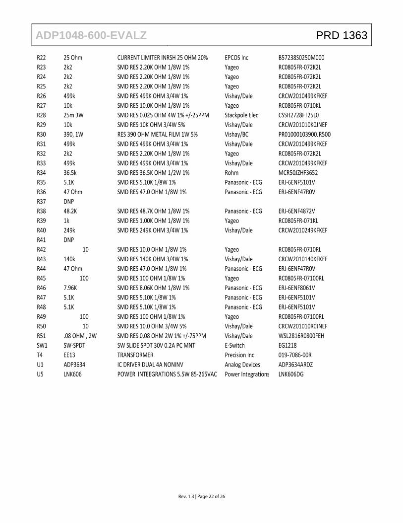
R22 25 Ohm CURRENT LIMITER INRSH 25 OHM 20% EPCOS Inc B57238S0250M000
R23 2k2 SMD RES 2.20K OHM 1/8W 1% Yageo RC0805FR‐072K2L
R24 2k2 SMD RES 2.20K OHM 1/8W 1% Yageo RC0805FR‐072K2L
R25 2k2 SMD RES 2.20K OHM 1/8W 1% Yageo RC0805FR‐072K2L
R26 499k SMD RES 499K OHM 3/4W 1% Vishay/Dale CRCW2010499KFKEF
R27 10k SMD RES 10.0K OHM 1/8W 1% Yageo RC0805FR‐0710KL
R28 25m 3W SMD RES 0.025 OHM 4W 1% +/‐25PPM Stackpole Elec CSSH2728FT25L0
R29 10k SMD RES 10K OHM 3/4W 5% Vishay/Dale CRCW201010K0JNEF
R30 390, 1W RES 390 OHM METAL FILM 1W 5% Vishay/BC PR01000103900JR500
R31 499k SMD RES 499K OHM 3/4W 1% Vishay/Dale CRCW2010499KFKEF
R32 2k2 SMD RES 2.20K OHM 1/8W 1% Yageo RC0805FR‐072K2L
R33 499k SMD RES 499K OHM 3/4W 1% Vishay/Dale CRCW2010499KFKEF
R34 36.5k SMD RES 36.5K OHM 1/2W 1% Rohm MCR50JZHF3652
R35 5.1K SMD RES 5.10K 1/8W 1% Panasonic ‐ ECG ERJ‐6ENF5101V
R36 47 Ohm SMD RES 47.0 OHM 1/8W 1% Panasonic ‐ ECG ERJ‐6ENF47R0V
R37 DNP
R38 48.2K SMD RES 48.7K OHM 1/8W 1% Panasonic ‐ ECG ERJ‐6ENF4872V
R39 1k SMD RES 1.00K OHM 1/8W 1% Yageo RC0805FR‐071KL
R40 249k SMD RES 249K OHM 3/4W 1% Vishay/Dale CRCW2010249KFKEF
R41 DNP
R42 10 SMD RES 10.0 OHM 1/8W 1% Yageo RC0805FR‐0710RL
R43 140k SMD RES 140K OHM 3/4W 1% Vishay/Dale CRCW2010140KFKEF
R44 47 Ohm SMD RES 47.0 OHM 1/8W 1% Panasonic ‐ ECG ERJ‐6ENF47R0V
R45 100 SMD RES 100 OHM 1/8W 1% Yageo RC0805FR‐07100RL
R46 7.96K SMD RES 8.06K OHM 1/8W 1% Panasonic ‐ ECG ERJ‐6ENF8061V
R47 5.1K SMD RES 5.10K 1/8W 1% Panasonic ‐ ECG ERJ‐6ENF5101V
R48 5.1K SMD RES 5.10K 1/8W 1% Panasonic ‐ ECG ERJ‐6ENF5101V
R49 100 SMD RES 100 OHM 1/8W 1% Yageo RC0805FR‐07100RL
R50 10 SMD RES 10.0 OHM 3/4W 5% Vishay/Dale CRCW201010R0JNEF
R51 .08 OHM , 2W SMD RES 0.08 OHM 2W 1% +/‐75PPM Vishay/Dale WSL2816R0800FEH
SW1 SW‐SPDT SW SLIDE SPDT 30V 0.2A PC MNT E‐Switch EG1218
T4 EE13 TRANSFORMER Precision Inc 019‐7086‐00R
U1 ADP3634 IC DRIVER DUAL 4A NONINV Analog Devices ADP3634ARDZ
U5 LNK606 POWER INTEEGRATIONS 5.5W 85‐265VAC Power Integrations LNK606DG

ADP1048-600-EVALZ PRD 1363
Rev. 1.3 | Page 23 of 26
APPENDIX XI – BILL OF MATERIALS (DAUGHTER CARD)
Part Reference Part Description Manufacture Mfg Part No
C1 DNI
C2 DNI
C3 DNI
C4 CAP CER 1000pF 50V 5% COG Murata Electronics GRM2165C1H102JA01D
C5 DNI
C6 DNI
C7 DNI
C8 DNI
C9 CAP CER 10uF 25V +/‐20% X5R Panasonic ‐ ECG ECJ‐4YB1E106M
C10 CAP CER 0.1uF 50V 10% X7R Murata Electronics GRM21BR71H104KA01L
C11 CAP CER 1.0uF 50V 10% X7R Murata Electronics GRM32RR71H105KA01L
C12 CAP CER 0.1uF 50V 10% X7R Murata Electronics GRM21BR71H104KA01L
C13 CAP CER 0.1uF 50V 10% X7R Murata Electronics GRM21BR71H104KA01L
C14 DNI
C15 DNI
C16 DNI
D1 DIODE SWITCH 100V 150MA Micro Commercial 1N4148WTPMSCT‐ND
D2 DIODE SWITCH 100V 150MA Micro Commercial 1N4148WTPMSCT‐ND
D6 LED SUPER RED CLEAR 75MA 1.7V SMD CHICAGO MINIATURE LIGHTING CMD15‐21SRC/TR8
R1 RES 90.9K OHM 1/8W 1% SMD Any
R2 RES 10K OHM 1/8W 1% SMD Any
R3 RES 90.9K OHM 1/8W 1% SMD Any
R4 RES 10K OHM 1/8W 1% SMD Any
R5 RES 90.9K OHM 1/8W 1% SMD Any
R6 RES 10K OHM 1/8W 1% SMD Any
R7 RES 10K OHM 1/8W 0.1% SMD Any
R8 RES 10K OHM 1/8W 0.1% SMD Any
R9 RES 0.0 OHM 1/8W 5% SMD Any
R11 RES 49.9K OHM 1/8W 0.1% SMD Any
R12 RES 2.20K OHM 1/8W 1% SMD Any
R13 RES 0.0 OHM 1/8W 5% SMD Any
R14 RES 10K OHM 1/8W 1% SMD Any
R15 RES 10K OHM 1/8W 1% SMD Any
R16 RES 0.0 OHM 1/8W 5% SMD Any
R18 RES 2.20K OHM 1/8W 1% SMD Any
R19 RES 2.20K OHM 1/8W 1% SMD Any
R20 RES 2.20K OHM 1/8W 1% SMD Any
R21 RES 2.20K OHM 1/8W 1% SMD Any
R22 RES 0.0 OHM 1/8W 5% SMD Any
U1 Digital PFC Controller Analog Devices ADP1047
U2 Low Dropout Regulators Analog Devices ADP3303

ADP1048-600-EVALZ PRD 1363
Rev. 1.3 | Page 24 of 26
APPENDIX XII – REGISTER FILE (REVA_IC REVISED-0408.48R)
Reg(1 h) = 4h - OPERATION
Reg(2 h) = 17h - ON_OFF_CONFIG
Reg(10 h) = 0h - WRITE_PROTECT
Reg(20 h) = 6h - VOUT_MODE
Reg(21 h) = 604h - VOUT_COMMAND
Reg(29 h) = 80AAh - VOUT_SCALE_LOOP
Reg(2A h) = FB02h - VOUT_SCALE_MONITOR
Reg(35 h) = F154h - VIN_ON
Reg(36 h) = F118h - VIN_OFF
Reg(40 h) = F708h - VOUT_OV_FAULT_Limit
Reg(41 h) = C0h - VOUT_OV_FAULT_RESPONSE
Reg(42 h) = F690h - VOUT_OV_WARN_LIMIT
Reg(43 h) = F500h - VOUT_UV_WARN_LIMIT
Reg(44 h) = F320h - VOUT_UV_FAULT_LIMIT
Reg(45 h) = 58h - VOUT_UV_FAULT_RESPONSE
Reg(50 h) = 0h - OT_FAULT_RESPONSE
Reg(55 h) = F434h - VIN_OV_FAULT_LIMIT
Reg(56 h) = 0h - VIN_OV_FAULT_RESPONSE
Reg(58 h) = F140h - VIN_UV_WARN_LIMIT
Reg(59 h) = F118h - VIN_UV_FAULT_LIMIT
Reg(5A h) = 78h - VIN_UV_FAULT_RESPONSE
Reg(5B h) = CA2Ah - IIN_OC_FAULT_LIMIT
Reg(5C h) = 0h - IIN_OC_FAULT_RESPONSE
Reg(5D h) = CA5Fh - IIN_OC_WARN_LIMIT_ADC
Reg(6B h) = F550h - PIN_OP_WARN_LIMIT
Reg(FE00 h) = 0h - CS_Fast_OCP_Response
Reg(FE01 h) = 80h - VFB_Fast_OVP_Response
Reg(FE02 h) = 0h - OLP_Response
Reg(FE03 h) = 0h - VDD3P3_RESPONSE
Reg(FE04 h) = 0h - VCORE_RESPONSE
Reg(FE05 h) = 0h - PGOOD_AC_OK_DEBOUNCE_SET
Reg(FE06 h) = 0h - PSON_SET
Reg(FE07 h) = 0h - Flag_Fault_ID
Reg(FE08 h) = 1Bh - SoftStart_Flags_Blank_1
Reg(FE09 h) = 0h - SoftStart_Flags_Blank_2
Reg(FE0A h) = 0h - PGOOD_FLAGS_LIST
Reg(FE0B h) = 0h - AC_OK_FLAGS_LIST
Reg(FE0C h) = 0h - PWM rising edge timing
Reg(FE0D h) = 0h - PWM rising edge setting
Reg(FE0E h) = 20h - PWM falling edge timing
Reg(FE0F h) = 3h - PWM falling edge setting
Reg(FE10 h) = 0h - PWM2 rising edge timing
Reg(FE11 h) = 0h - PWM2 rising edge setting
Reg(FE12 h) = 20h - PWM2 falling edge timing
Reg(FE13 h) = 3h - PWM2 falling edge setting
Reg(FE14 h) = 1h - PWM_Set
Reg(FE15 h) = 33h - PWM_Limit
Reg(FE18 h) = 83h - RTD_ADC_gain_Trim
Reg(FE19 h) = 0h - OT_FAULT_LIMIT
Reg(FE1A h) = 0h - OT_WARN_LIMIT
Reg(FE1B h) = Dh - Switching frequency setting
Reg(FE1C h) = 0h - Low power switching frequency setting
Reg(FE1D h) = 3h - Frequency dithering set
Reg(FE1E h) = 0h - Frequency synchronization set
Reg(FE20 h) = 28h - Voltage_Loop_Filter_Gain
Reg(FE21 h) = C0h - Voltage_Loop_Filter_Zero
Reg(FE22 h) = 58h - Fast voltage loop filter gain
Reg(FE23 h) = F8h - Fast voltage loop filter zero
Reg(FE24 h) = BBh - Fast voltage loop enable
Reg(FE25 h) = 4Ah - VAC_threshold_set
Reg(FE27 h) = 4Bh - MIN_AC_PERIOD_SET
Reg(FE28 h) = 8Ah - MAX_AC_PERIOD_SET
Reg(FE29 h) = 32h - Current loop filter gain for low line input
Reg(FE2A h) = D7h - Current loop filter zero for low line input
Reg(FE2B h) = 5Ah - Current loop filter gain for high line input
Reg(FE2C h) = AAh - Current loop filter zero for high line input
Reg(FE2D h) = 1Eh - Soft_Start_Set
Reg(FE2E h) = 1h - INRUSH_Set
Reg(FE2F h) = 32h - VFB_OV_FAULT_RISE
Reg(FE30 h) = 3h - VFB_OV_FAULT_FALL
Reg(FE31 h) = 2h - FAST_OVP_debounce_setting
Reg(FE32 h) = 2Eh - Low power mode operation threshold
Reg(FE35 h) = 4Dh - HIGH LINE LIMIT
Reg(FE36 h) = 41h - LOW LINE LIMIT
Reg(FE37 h) = 0h - Ilim_trim
Reg(FE39 h) = 6B7h - EXPONENT
Reg(FE3A h) = 3h - READ_UPD_RATE
Reg(FE3B h) = FB02h - VIN_SCALE_MONITOR
Reg(FE3C h) = DB20h - IIN_RSENSE
Reg(FE3D h) = 1Fh - FAST_OCP_BLANK
Reg(FE3E h) = E0h - CS_Fast_OCP_setting
Reg(FE3F h) = 0h - Temperature hysteresis
Reg(FE40 h) = 28h - VAC_ADC_gain_Trim
ADP1048-600-EVALZ PRD 1363
Rev. 1.3 | Page 25 of 26
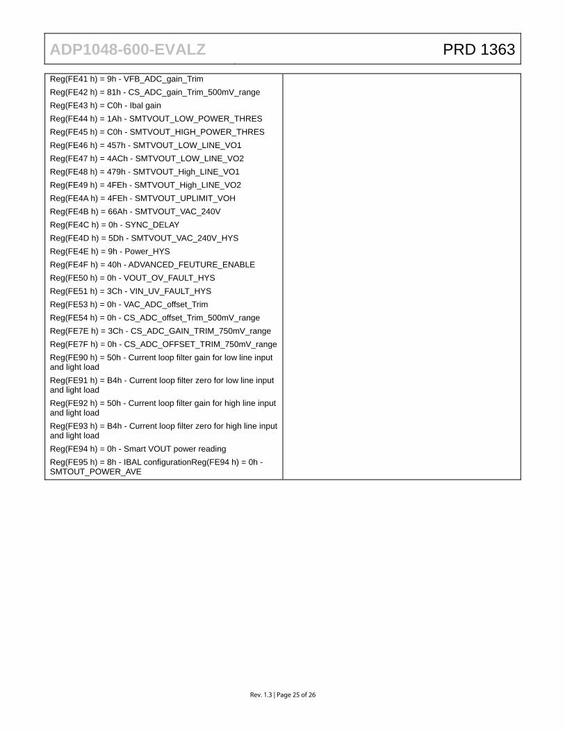
Reg(FE41 h) = 9h - VFB_ADC_gain_Trim
Reg(FE42 h) = 81h - CS_ADC_gain_Trim_500mV_range
Reg(FE43 h) = C0h - Ibal gain
Reg(FE44 h) = 1Ah - SMTVOUT_LOW_POWER_THRES
Reg(FE45 h) = C0h - SMTVOUT_HIGH_POWER_THRES
Reg(FE46 h) = 457h - SMTVOUT_LOW_LINE_VO1
Reg(FE47 h) = 4ACh - SMTVOUT_LOW_LINE_VO2
Reg(FE48 h) = 479h - SMTVOUT_High_LINE_VO1
Reg(FE49 h) = 4FEh - SMTVOUT_High_LINE_VO2
Reg(FE4A h) = 4FEh - SMTVOUT_UPLIMIT_VOH
Reg(FE4B h) = 66Ah - SMTVOUT_VAC_240V
Reg(FE4C h) = 0h - SYNC_DELAY
Reg(FE4D h) = 5Dh - SMTVOUT_VAC_240V_HYS
Reg(FE4E h) = 9h - Power_HYS
Reg(FE4F h) = 40h - ADVANCED_FEUTURE_ENABLE
Reg(FE50 h) = 0h - VOUT_OV_FAULT_HYS
Reg(FE51 h) = 3Ch - VIN_UV_FAULT_HYS
Reg(FE53 h) = 0h - VAC_ADC_offset_Trim
Reg(FE54 h) = 0h - CS_ADC_offset_Trim_500mV_range
Reg(FE7E h) = 3Ch - CS_ADC_GAIN_TRIM_750mV_range
Reg(FE7F h) = 0h - CS_ADC_OFFSET_TRIM_750mV_range
Reg(FE90 h) = 50h - Current loop filter gain for low line input and light load
Reg(FE91 h) = B4h - Current loop filter zero for low line input and light load
Reg(FE92 h) = 50h - Current loop filter gain for high line input and light load
Reg(FE93 h) = B4h - Current loop filter zero for high line input and light load
Reg(FE94 h) = 0h - Smart VOUT power reading
Reg(FE95 h) = 8h - IBAL configurationReg(FE94 h) = 0h - SMTOUT_POWER_AVE

ADP1048-600-EVALZ PRD 1363
Rev. 1.3 | Page 26 of 26
NOTES
©2009 Analog Devices, Inc. All rights reserved. Trademarks and registered trademarks are the property of their respective owners. Error! Unknow