Embed Size (px)
Citation preview

ADM-PCIE-9V3User Manual
Document Revision: 2.513th Jul 2018

ADM-PCIE-9V3 User Manual
© 2018 Copyright Alpha Data Parallel Systems Ltd.All rights reserved.
This publication is protected by Copyright Law, with all rights reserved. No part of thispublication may be reproduced, in any shape or form, without prior written consent from Alpha
Data Parallel Systems Ltd.
Head Office
Address: 4 West Silvermills LaneEdinburgh, EH3 5BD, UK
Telephone: +44 131 558 2600Fax: +44 131 558 2700email: [email protected]: http://www.alpha-data.com
US Office
611 Corporate Circle, Suite HGolden, CO 80401(303) 954 8768(866) 820 9956 - toll [email protected]://www.alpha-data.com
All trademarks are the property of their respective owners.
ADM-PCIE-9V3 User Manual
Table Of Contents
1 Introduction ...................................................................................................................................... 1 1.1 Key Features ................................................................................................................................. 1 1.2 Order Code .................................................................................................................................... 12 PCB Information .............................................................................................................................. 2 2.1 Physical Specifications .................................................................................................................. 2 2.2 Chassis Requirements ................................................................................................................... 2 2.2.1 PCI Express ............................................................................................................................... 2 2.2.2 Mechanical Requirements ......................................................................................................... 2 2.2.3 Power Requirements ................................................................................................................. 2 2.3 Thermal Performance .................................................................................................................... 3 2.4 Optional Blower ............................................................................................................................. 33 Functional Description .................................................................................................................... 4 3.1 Overview ........................................................................................................................................ 4 3.1.1 Switches .................................................................................................................................... 5 3.1.2 LEDs .......................................................................................................................................... 6 3.2 Clocking ......................................................................................................................................... 7 3.2.1 PCIe Reference Clocks ............................................................................................................. 7 3.2.2 Fabric Clock ............................................................................................................................... 7 3.2.3 Programming Clock (EMCCLK) ................................................................................................. 8 3.2.4 QSFP28 ..................................................................................................................................... 8 3.2.5 Ultraport SlimSAS ...................................................................................................................... 9 3.2.6 DDR4 SDRAM Reference Clocks .............................................................................................. 9 3.3 PCI Express ................................................................................................................................. 10 3.4 DDR4 SDRAM ............................................................................................................................. 10 3.5 QSFP28 ....................................................................................................................................... 11 3.6 OpenCAPI Ultraport SlimSAS ...................................................................................................... 12 3.7 System Monitor ............................................................................................................................ 13 3.7.1 System Monitor Status LEDs ................................................................................................... 14 3.8 USB Interface .............................................................................................................................. 15 3.9 Configuration ............................................................................................................................... 15 3.9.1 Configuration From Flash Memory .......................................................................................... 15 3.9.1.1 Building and Programming Configuration Images ............................................................... 16 3.9.2 Configuration via JTAG ............................................................................................................ 16 3.10 GPIO Connector .......................................................................................................................... 17 3.10.1 Direct Connect FPGA Signals .................................................................................................. 17 3.10.2 Timing Input ............................................................................................................................. 17 3.11 User EEPROM ............................................................................................................................. 18
Appendix A Complete Pinout Table .................................................................................................................. 19
List of Tables
Table 1 Mechanical Dimensions ..................................................................................................................... 2Table 2 Available Power By Rail ..................................................................................................................... 2Table 3 Switch Functions ................................................................................................................................ 5Table 4 LED Details ........................................................................................................................................ 6Table 5 PCIe Reference Clocks ..................................................................................................................... 7Table 6 Fabric Clock ....................................................................................................................................... 8Table 7 EMCCLK ............................................................................................................................................ 8Table 8 QSFP28 Reference Clocks ................................................................................................................ 8
ADM-PCIE-9V3 User Manual
Table 9 QSFP28 Jitter Attenuated Reference Clocks ..................................................................................... 8Table 10 SlimSAS Reference Clocks (OpenCAPI) ........................................................................................... 9Table 11 Memory Reference Clocks ................................................................................................................ 9Table 12 QSFP28 Part Numbers .................................................................................................................... 11Table 13 Voltage, Current, and Temperature Monitors ................................................................................... 13Table 14 Status LED Definitions ..................................................................................................................... 14Table 15 Complete Pinout Table ..................................................................................................................... 19
List of Figures
Figure 1 ADM-PCIE-9V3 Product Photo .......................................................................................................... 1Figure 2 Thermal Performance ........................................................................................................................ 3Figure 3 Optional Blower ................................................................................................................................. 3Figure 4 ADM-PCIE-9V3 Block Diagram ......................................................................................................... 4Figure 5 Switches ............................................................................................................................................ 5Figure 6 Backside LEDs .................................................................................................................................. 6Figure 7 Front Panel LEDs .............................................................................................................................. 6Figure 8 Clock Topology .................................................................................................................................. 7Figure 9 Si5328 Block Diagram ....................................................................................................................... 9Figure 10 QSFP Locations ............................................................................................................................... 11Figure 11 OpenCAPI Location ......................................................................................................................... 12Figure 12 Flash Address Map .......................................................................................................................... 15Figure 13 GPIO Connector Schematic ............................................................................................................ 17Figure 14 GPIO Connector Location ................................................................................................................ 17

ADM-PCIE-9V3 User Manual
1 IntroductionThe ADM-PCIE-9V3 is a high-performance reconfigurable computing card intended for Data Center applications,featuring a Xilinx Virtex UltraScale Plus FPGA.
Figure 1 : ADM-PCIE-9V3 Product Photo
1.1 Key FeaturesKey Features
• PCIe Gen1/2/3 x1/2/4/8/16 capable• Half-length, low-profile x16 PCIe form factor• Two banks of DDR4 SDRAM 72 bit wide memory (ECC), 16GB (8GB per bank) default rated at 2400MT/s,
32GB option rated at 1866MT/s.• Two QSFP28/zQSFP+ sites capable of data rates up to 28 Gbps per channel (112 Gbps per cage)• One 8 lane Ultraport SlimSAS connector that is compliant with OpenCAPI• Optional timing input• Front panel and rear edge JTAG access via USB port• FPGA configurable over USB/JTAG and SPI configuration flash• XCVU3P-2FFVC1517I FPGA• Voltage, current, and temperature monitoring
1.2 Order CodeADM-PCIE-9V3
See http://www.alpha-data.com/pdfs/adm-pcie-9v3.pdf for complete ordering options.
Page 1Introductionad-ug-1322_v2_5.pdf
ADM-PCIE-9V3 User Manual
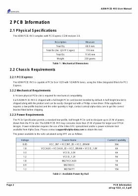
2 PCB Information2.1 Physical Specifications
The ADM-PCIE-9V3 complies with PCI Express CEM revision 3.0.
Description Measure
Total Dy 68.9 mm
Total Dx (Inc. QSFP Cages) 174 mm
Total Dz 17.45 mm
Weight 230 grams
Table 1 : Mechanical Dimensions
2.2 Chassis Requirements
2.2.1 PCI Express
The ADM-PCIE-9V3 is capable of PCIe Gen 1/2/3 with 1/2/4/8/16 lanes, using the Xilinx Integrated Block for PCIExpress.
2.2.2 Mechanical Requirements
A 16-lane physical PCIe slot is required for mechanical compatibility.
Each ADM-PCIE-9V3 is shipped with a full height PCIe card bracket installed by default. A half-height bracket isshipped along with the product and can be easily changed out with a Philips screw driver. If the applicationrequires a low-profile bracket and the order quantity is high, contact [email protected] to get the correctbracket fitted before shipping.
2.2.3 Power Requirements
The PCIe Specification permits a standard low-profile, half-length PCIe card to dissipate up to 25 W of power,drawn from the PCIe slot. The ADM-PCIE-9V3 may consume more than 25 W of power for larger user FPGAdesigns. Power estimation requires the use of the Xilinx XPE spreadsheet and/or a power estimator toolavailable from Alpha Data. Please contact [email protected] to obtain this tool.
The power available to the rails calculated using XPE are as follows:
Voltage Source Name Current Capability
0.85 VCC_INT + VCCINT_IO + VCC_BRAM 36A
1.8 VCCAUX + VCCAUX_IO + VCC_BRAM + VCCO_1.8V 6A
3.3 VCCO_3.3V 6A
1.2 VCCO_1.2V 9A
1.8 MGTVCCAUX 1A
0.9 MGTAVCC 9A
1.2 MGTAVTT 15A
Table 2 : Available Power By Rail
Page 2 PCB Informationad-ug-1322_v2_5.pdf
ADM-PCIE-9V3 User Manual
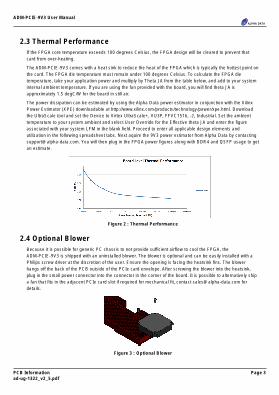
2.3 Thermal PerformanceIf the FPGA core temperature exceeds 100 degrees Celsius, the FPGA design will be cleared to prevent thatcard from over-heating.
The ADM-PCIE-9V3 comes with a heat sink to reduce the heat of the FPGA which is typically the hottest point onthe card. The FPGA die temperature must remain under 100 degrees Celsius. To calculate the FPGA dietemperature, take your application power and multiply by Theta JA from the table below, and add to your systeminternal ambient temperature. If you are using the fan provided with the board, you will find theta JA isapproximately 1.5 degC/W for the board in still air.
The power dissipation can be estimated by using the Alpha Data power estimator in conjunction with the XilinxPower Estimator (XPE) downloadable at http://www.xilinx.com/products/technology/power/xpe.html. Downloadthe UltraScale tool and set the Device to Virtex UltraScale+, VU3P, FFVC1516, -2, Industrial. Set the ambienttemperature to your system ambient and select User Override for the Effective theta JA and enter the figureassociated with your system LFM in the blank field. Proceed to enter all applicable design elements andutilization in the following spreadsheet tabs. Next aquire the 9V3 power estimator from Alpha Data by [email protected]. You will then plug in the FPGA power figures along with DDR4 and QSFP usage to getan estimate.
Figure 2 : Thermal Performance
2.4 Optional BlowerBecause it is possible for generic PC chassis to not provide sufficient airflow to cool the FPGA, theADM-PCIE-9V3 is shipped with an uninstalled blower. The blower is optional and can be easily installed with aPhilips screw driver at the discretion of the user. Ensure the opening is facing the heatsink fins. The blowerhangs off the back of the PCB outside of the PCIe card envelope. After screwing the blower into the heatsink,plug in the small power connector into the connector in the corner of the board. It is possible to alternatively shipa fan that fits in the adjacent PCIe card slot if required for mechanical fit, contact [email protected] fordetails.
Figure 3 : Optional Blower
Page 3PCB Informationad-ug-1322_v2_5.pdf
ADM-PCIE-9V3 User Manual
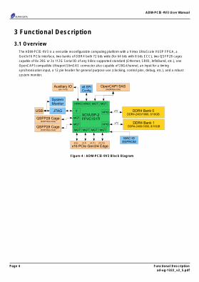
3 Functional Description3.1 Overview
The ADM-PCIE-9V3 is a versatile reconfigurable computing platform with a Virtex UltraScale VU3P FPGA, aGen3x16 PCIe interface, two banks of DDR4 both 72 bits wide (for 64 bits with 8 bits ECC), two QSFP28 cagescapable of 8x 28G or 2x 112G Serial IO of any Xilinx supported standard (Ethernet, SRIO, Infiniband, etc.), oneOpenCAPI compatible Ultraport SlimSAS connector also capable of 28G/channel, an input for a timingsynchronization input, a 12 pin header for general purpose use (clocking, control pins, debug, etc.), and a robustsystem monitor.
XCVU3P-2FFVC1517I
(0,4) (5,7) (8,11) (12,15)
x16 PCIe Gen3/4 Edge
QSFP28 Cage(4x28 Gbps max)
QSFP28 Cage(4x28 Gbps max) DDR4 Bank 1
DDR4-2400/1866, 8/16GB
DDR4 Bank 0DDR4-2400/1866, 8/16GB
SystemMonitor
MGT
MGT HPIO
HPIO
HRIO
x8 SPIConfig
x72
x72
MGTMGT MGT
HRIO
USB JTAG 0
Auxiliary IO(gpio, timing)
MGTMGT
OpenCAPI SAS(8x28Gbps max)
MGT
MAC IDEEPROM
Figure 4 : ADM-PCIE-9V3 Block Diagram
Page 4 Functional Descriptionad-ug-1322_v2_5.pdf
ADM-PCIE-9V3 User Manual
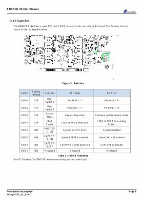
3.1.1 Switches
The ADM-PCIE-9V3 has a quad DIP switch SW1, located on the rear side of the board. The function of eachswitch in SW1 is detailed below:
Figure 5 : Switches
Switch FactoryDefault Function OFF State ON State
SW1-1 OFF UserSwitch 0 Pin AV27 = '1' Pin AV27 = '0'
SW1-2 OFF UserSwitch 1 Pin AW27 = '1' Pin AW27 = '0'
SW1-3 OFF ServiceMode Regular Operation Firmware update service mode
SW1-4 OFF JTAGSource JTAG to FPGA from USB JTAG to FPGA from debug
header
SW2-1 ON HOST_I2C_EN Sysmon over PCIe I2C Sysmon isolated
SW2-2 ON CAPI_VPD_EN OpenCAPI VPD available OpenCAPI VPD isolated
SW2-3 ON CAPI_VPD_WP CAPI VPD is write protected CAPI VPD is writable
SW2-4 ON Reserved Reserved Reserved
Table 3 : Switch FunctionsUse IO Standard "LVCMOS18" when constraining the user switch pin.
Page 5Functional Descriptionad-ug-1322_v2_5.pdf
ADM-PCIE-9V3 User Manual
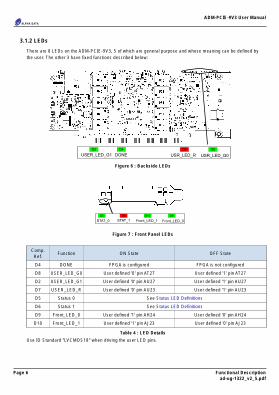
3.1.2 LEDs
There are 8 LEDs on the ADM-PCIE-9V3, 5 of which are general purpose and whose meaning can be defined bythe user. The other 3 have fixed functions described below:
USR_LED_G0
D2 D4 D7 D8
USER_LED_G1 USR_LED_RDONE
Figure 6 : Backside LEDs
Front_LED_0
D5 D6 D9
Front_LED_1STAT_0 STAT_1D10
Figure 7 : Front Panel LEDs
Comp.Ref. Function ON State OFF State
D4 DONE FPGA is configured FPGA is not configured
D8 USER_LED_G0 User defined '0' pin AT27 User defined '1' pin AT27
D2 USER_LED_G1 User defined '0' pin AU27 User defined '1' pin AU27
D7 USER_LED_R User defined '0' pin AU23 User defined '1' pin AU23
D5 Status 0 See Status LED Definitions
D6 Status 1 See Status LED Definitions
D9 Front_LED_0 User defined '1' pin AH24 User defined '0' pin AH24
D10 Front_LED_1 User defined '1' pin AJ23 User defined '0' pin AJ23
Table 4 : LED DetailsUse IO Standard "LVCMOS18" when driving the user LED pins.
Page 6 Functional Descriptionad-ug-1322_v2_5.pdf
ADM-PCIE-9V3 User Manual
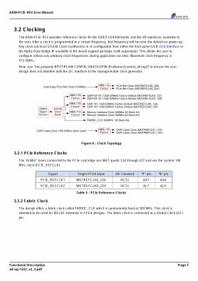
3.2 ClockingThe ADM-PCIE-9V3 provides reference clocks for the DDR4 SDRAM banks and the I/O interfaces available tothe user. After a clock is programmed to a certain frequency, that frequency will become the default on power-up.Any clock out of an Si5338 Clock Synthesizer is re-configurable from either the front panel USB USB Interface orthe Alpha Data bridge IP available in the board support package (sold separately). This allows the user toconfigure almost any arbitrary clock frequencies during application run time. Maximum clock frequency is312.5MHz.
Note: use "set_property BITSTREAM.CONFIG.UNUSEDPIN {Pullnone} [current_design]" to ensure the userdesign does not interfere with the I2C interface to the reprogramable clock generator.
NB6L11SFanout QSFP28 161.1328125MHz Factory Default (MGTREFCLK0_128)
QSFP28 161.1328125MHz Factory Default (MGTREFCLK0_127)
FABRIC_CLK 300MHz (IO Bank 64)
Card Edge PCIe Ref Clock (100MHz)
25MHz30ppmSource
Si5338ClockSynth
NB6L11SFanout CAPI 161.1328125MHz Factory Default (MGTREFCLK0_125)
CAPI 161.1328125MHz Factory Default (MGTREFCLK0_124)
NB6L11SFanout
Memory Interface Clock 300Mhz (IO Bank 44)Memory Interface Clock 300Mhz (IO Bank 64)
NB6L11SFanout PCIe Ref Clock (MGTREFCLK0_224)
PCIe Ref Clock (MGTREFCLK0_226)
CAPI Cable Clock (156.25MHz when used)NB6L11SFanout CAPI Cable Clock (MGTREFCLK1_125)
CAPI Cable Clock (MGTREFCLK1_124)
Figure 8 : Clock Topology
3.2.1 PCIe Reference Clocks
The 16 MGT lanes connected to the PCIe card edge use MGT quads 224 through 227 and use the system 100MHz clock (PCIE_REFCLK).
Signal Target FPGA Input I/O Standard "P" pin "N" pin
PCIE_REFCLK1 MGTREFCLK0_226 HCSL AA7 AA6
PCIE_REFCLK2 MGTREFCLK0_224 HCSL AJ7 AJ6
Table 5 : PCIe Reference Clocks
3.2.2 Fabric Clock
The design offers a fabric clock called FABRIC_CLK which is permanently fixed at 300 MHz. This clock isintended to be used for IDELAY elements in FPGA designs. The fabric clock is connected to a Global Clock (GC)pin.
Page 7Functional Descriptionad-ug-1322_v2_5.pdf
ADM-PCIE-9V3 User Manual
Signal Target FPGA Input I/O Standard "P" pin "N" pin
FABRIC_CLK IO_L12P_T1U_GC_64 LVDS AP26 AP27
Table 6 : Fabric ClockDIFF_TERM_ADV = TERM_100 is required for LVDS termination
3.2.3 Programming Clock (EMCCLK)
An 100MHz clock is fed into the EMCCLK pin to drive the SPI flash device during configuration of the FPGA.Note that this is not a global clock capable IO pin.
Signal Target FPGA Input I/O Standard pin
REFCLK100M IO_L24P_T3U_N10_EMCCLK_65 LVCMOS18 AJ28
Table 7 : EMCCLK
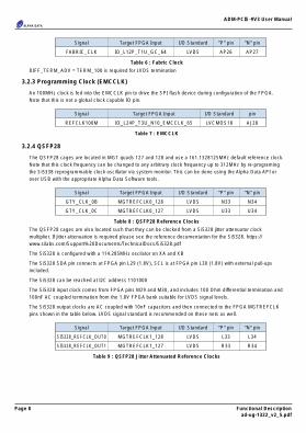
3.2.4 QSFP28
The QSFP28 cages are located in MGT quads 127 and 128 and use a 161.1328125MHz default reference clock.Note that this clock frequency can be changed to any arbitrary clock frequency up to 312MHz by re-programingthe Si5338 reprogrammable clock oscillator via system monitor. This can be done using the Alpha Data API orover USB with the appropriate Alpha Data Software tools.
Signal Target FPGA Input I/O Standard "P" pin "N" pin
GTY_CLK_0B MGTREFCLK0_128 LVDS N33 N34
GTY_CLK_0C MGTREFCLK0_127 LVDS U33 U34
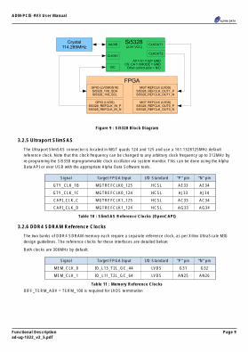
Table 8 : QSFP28 Reference ClocksThe QSFP28 cages are also located such that they can be clocked from a Si5328 jitter attenuator clockmultiplier. If jitter attenuation is required please see the reference documentation for the Si5328. https://www.silabs.com/Support%20Documents/TechnicalDocs/Si5328.pdf
The Si5328 is configured with a 114.285MHz oscilator on XA and XB
The Si5328 SDA pin connects at FPGA pin L29 (1.8V), SCL is at FPGA pin L30 (1.8V) with external pull-upsincluded.
The Si5328 can be reached at I2C address 1101000
The Si5328 input clock comes from FPGA pins M29 and M30, and includes 100 Ohm differential termination and100nF AC coupled termination from the 1.8V FPGA bank suitable for LVDS signal levels.
The Si5328 output clocks are AC coupled with 10nF capacitors and then connected to the FPGA MGTREFCLKpins shown in the table below. LVDS signal standard is recommended on these nets as well.
Signal Target FPGA Input I/O Standard "P" pin "N" pin
SI5328_REFCLK_OUT0 MGTREFCLK1_128 LVDS L33 L34
SI5328_REFCLK_OUT1 MGTREFCLK1_127 LVDS R33 R34
Table 9 : QSFP28 Jitter Attenuated Reference Clocks
Page 8 Functional Descriptionad-ug-1322_v2_5.pdf
ADM-PCIE-9V3 User Manual
FPGA
Si5328 (2.5V VCC)
A0 = A1 = A2= GNDCS_CA = CMODE = GND
Other control pins = N/C
GPIO (LVCMOS18)SI5328_1V8_SDASI5328_1V8_SCL
I2C
CLKOUT2
CLKOUT1Crystal
114.285MHzXA/XB
CLKIN1
GPIO (LVDS)SI5328_REFCLK_IN_PSI5328_REFCLK_IN_N
MGT REFCLK (LVDS)SI5328_REFCLK_OUT0_PSI5328_REFCLK_OUT0_N
MGT REFCLK (LVDS)SI5328_REFCLK_OUT1_PSI5328_REFCLK_OUT1_N
Figure 9 : Si5328 Block Diagram
3.2.5 Ultraport SlimSAS
The Ultraport SlimSAS connector is located in MGT quads 124 and 125 and use a 161.1328125MHz defaultreference clock. Note that this clock frequency can be changed to any arbitrary clock frequency up to 312MHz byre-programing the Si5338 reprogrammable clock oscillator via system monitor. This can be done using the AlphaData API or over USB with the appropriate Alpha Data Software tools.
Signal Target FPGA Input I/O Standard "P" pin "N" pin
GTY_CLK_1B MGTREFCLK0_125 HCSL AE33 AE34
GTY_CLK_1C MGTREFCLK0_124 HCSL AJ33 AJ34
CAPI_CLK_C MGTREFCLK1_125 HCSL AC33 AC34
CAPI_CLK_D MGTREFCLK1_124 HCSL AG33 AG34
Table 10 : SlimSAS Reference Clocks (OpenCAPI)
3.2.6 DDR4 SDRAM Reference Clocks
The two banks of DDR4 SDRAM memory each require a separate reference clock, as per Xilinx UltraScale MIGdesign guidelines. The reference clocks for these interfaces are detailed below:
Both clocks are 300MHz by default.
Signal Target FPGA Input I/O Standard "P" pin "N" pin
MEM_CLK_0 IO_L13_T2L_GC_44 LVDS G31 G32
MEM_CLK_1 IO_L11_T2L_GC_64 LVDS AN25 AN26
Table 11 : Memory Reference ClocksDIFF_TERM_ADV = TERM_100 is required for LVDS termination
Page 9Functional Descriptionad-ug-1322_v2_5.pdf
ADM-PCIE-9V3 User Manual
3.3 PCI ExpressThe ADM-PCIE-9V3 is capable of PCIe Gen 1/2/3 with 1/2/4/8/16 lanes. The FPGA drives these lanes directlyusing the Integrated PCI Express block from Xilinx. Negotiation of PCIe link speed and number of lanes used isgenerally automatic and does not require user intervention.
PCI Express reset (PERST#) connected to the FPGA at two locations. See Complete Pinout Table signalsPERST_1V8_0 and PERST_1V8_1.
The other pin assignments for the high speed lanes are provided in the pinout attached to the Complete PinoutTable
The PCI Express specification requires that all add-in cards be ready for enumeration within 120ms after poweris valid (100ms after power is valid + 20ms after PERST is released). The ADM-PCIE-9V3 does meet thisrequirement when configured from a tandem bitstream with the proper SPI constraints detailed in the section:Configuration From Flash Memory. For more details on tandem configuration, see Xilinx xapp 1179.
Note: Different motherboards/backplanes will benefit from different RX equalization schemes within the PCIe IP coreprovided by Xilinx. Alpha Data recommends using the following setting if a user experiences link errors ortraining issues with their system: within the IP core generator, change the mode to "Advanced" and open the"GT Settings" tab, change the "form factor driven insertion loss adjustment" from "Add-in Card" to"Chip-to-Chip" (See Xilinx PG239 for more details).
3.4 DDR4 SDRAMTwo banks of DDR4 SDRAM memory are soldered down to the board. While the factory default is 8GB/per bank,16GB/bank is also supported through a built variant. Please see Order Code for all order options. The memoryinterface is 72-bit wide data (64 data + 8 ECC). Maximum signaling rate is 2400 MT/s for 16GB total and1688MT/s with 32GB total.
Memory solutions are available from the Xilinx Memory Interface Generator (MIG) tool. An example memoryexerciser project is included in the ADM-PCIE-9V3 SDK. All constraint information is included in Complete PinoutTable. Alpha Data has also provided a custom csv timing file for use with Xilinx MIG. This can be downloadedfrom the ADM-PCIE-9V3 product page.
8Gb components used (standard) are Micron MT40A1G8PM-083E
16Gb components used (build variant) are Micron MT40A2G8PM-093E
Page 10 Functional Descriptionad-ug-1322_v2_5.pdf

ADM-PCIE-9V3 User Manual
3.5 QSFP28Two QSFP28 cages are available at the front panel. Both cages are capable of housing either active optical orpassive copper QSFP28 or QSFP compatible components. The communication interface can run at up to28Gbps per channel. There are eight channels between the two QSFP28 cages (total maximum bandwidth of224Gbps). These cages are ideally suited for 8x 25G or 2x 100G Ethernet or any other protocol supported by theXilinx GTY Transceivers. Please see Xilinx User Guide UG578 for more details on the capabilities of thetransceivers.
Both QSFP28 cages have control signals connected to the FPGA. Their connectivity is detailed in the CompletePinout Table at the end of this document. The notation used in the pin assignments is QSFP0 and QSFP1 withlocations clarified in the diagram below.
Use the QSFP*_SEL_1V8_L in conjunction with the OPTICAL_SCL_1V8 and OPTICAL_SDA_1V8 pins asdetailed in Complete Pinout Table to communicate with QSFP28 register space.
Note: The LP_MODE (Low Power Mode) to each QSFP28 cage is tied to ground.
Figure 10 : QSFP Locations
The order options for the ADM-PCIE-9V3 include an option to fit the QSFP28 optical transceivers. The tablebelow shows the part number for the transceivers fitted with each option.
Order Code Description Part Number Manufacturer
Q10 40G (4x10) QSFP Optical Transceiver FTL410QE2C Finisar
Q14 56G (4x14) QSFP Optical Transceiver FTL414QB2C Finisar
Q25 100G (4x25) QSFP28 Optical Transceiver FTLC9551REPM Finisar
Table 12 : QSFP28 Part Numbers
Page 11Functional Descriptionad-ug-1322_v2_5.pdf

ADM-PCIE-9V3 User Manual
3.6 OpenCAPI Ultraport SlimSASAn Ultraport SlimSAS receptacles along the top of the board allows for OpenCAPI compliant interfaces runningat 200G (8 chanels at 25G). Please contact [email protected] or your IBM representative for more detailson OpenCAPI and its benefits.
The SlimSAS connector can also be used to connect multiple 9V3 cards within a chassis.
Figure 11 : OpenCAPI Location
Page 12 Functional Descriptionad-ug-1322_v2_5.pdf
ADM-PCIE-9V3 User Manual
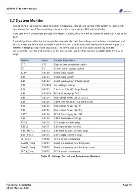
3.7 System MonitorThe ADM-PCIE-9V3 has the ability to monitor temperature, voltage, and current of the system to check on theoperation of the board. The monitoring is implemented using an Atmel AVR microcontroller.
If the core FPGA temperature exceeds 100 degrees Celsius, the FPGA will be cleared to prevent damage to thecard.
Control algorithms within the microcontroller automatically check line voltages and on board temperatures andshares makes the information available to the FPGA over a dedicated serial interface built into the Alpha Datareference design package (sold separately). The information can also be accessed directly from themicrocontroller over the USB interface on the front panel or via the IPMI interface available at the PCIe cardedge.
Monitors Index Purpose/Description
ETC ETC Elapsed time counter (seconds)
EC EC Event counter (power cycles)
12.0V ADC00 Board Input Supply
3.3V ADC01 Board Input Supply
3.3V ADC02 Board Input Auxilary Power Supply
3.3V PSU0OK Internal logic voltage
2.5V ADC03 Clock and DRAM Voltage Supply
1.8V PSU0OK FPGA IO Voltage (VCCO)
1.8V ADC04 Transceiver Power (AVCC_AUX)
1.2V ADC05 DDR4 SDRAM and FPGA memory I/O
1.2V ADC06 Transceiver Power (AVTT)
0.9V ADC07 Transceiver Power (AVCC)
0.85V ADC08 FPGA Core Supply (VccINT)
0.6V ADC09 DDR4 Termination Voltage
12V_I ADC10 12V input current in amps
3.3V_I ADC11 3.3V input current in amps
1.8V_MGT_I ADC12 1.8V MGT supply current in amps
2.5V_DIG_I ADC13 2.5V supply current in amps
uC_Temp TMP00 FPGA on-die temperature
Board0_Temp TMP01 Board temperature near front panel
Board1_Temp TMP02 Board temperature near back top corner
FPGA_Temp TMP03 FPGA on-die temperature
Table 13 : Voltage, Current, and Temperature Monitors
Page 13Functional Descriptionad-ug-1322_v2_5.pdf

ADM-PCIE-9V3 User Manual
3.7.1 System Monitor Status LEDs
LEDs D6 (Red) and D5 (Green) indicate the card health status.
LEDs Status
Green Running and no alarms
Green + Red Standby (Powered off)
Flashing Green + Flashing Red(together) Attention - critical alarm active
Flashing Green + Flashing Red(alternating) Service Mode
Flashing Green + Red Attention - alarm active
Red Missing application firmware orinvalid firmware
Flashing Red FPGA configuration cleared toprotect board
Table 14 : Status LED Definitions
Page 14 Functional Descriptionad-ug-1322_v2_5.pdf
ADM-PCIE-9V3 User Manual
3.8 USB InterfaceFor convenience the FPGA can be configured directly from the USB connection on either the front panel or therear card edge (rear edge in rev7, sn306 and newer). The ADM-PCIE-9V3 utilizes the Digilent USB-JTAGconverter box which is supported by the Xilinx software tool suite. Simply connect a micro-USB AB type cablebetween the ADM-PCIE-9V3 USB port and a host computer with Vivado installed. Vivado Hardware Manager willautomatically recognize the FPGA and allow you to configure the FPGA and the SBPI configuration PROM.
The same USB connector is used to directly access the system monitor system. All voltages, currents,temperatures, and non-volatile clock configuration settings can be accessed using Alpha Data's avr2util softwareat this interface.
Avr2util and associated windows USB driver is downloadable here:ftp://ftp.alpha-data.com/pub/firmware/utilities/windows/
Use "avr2util.exe /?" to see all options.
For example "avr2util.exe /usbcom com4 display-sensors" will desiplay all sensor values.
For example "avr2util.exe /usbcom com4 setclknv 0 156250000" will set the QSFP clock to 156.25MHz. setclkindex 1 = CAPI, index 2 = Memory, index 3 = Fabric.
Change 'com4' to match the com port number assigned under windows device manager.
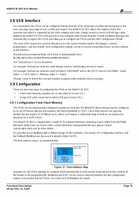
3.9 ConfigurationThere are two main ways of configuring the FPGA on the ADM-PCIE-9V3:
• From Flash memory, at power-on, as described in Section 3.9.1
• Using USB cable connected at either USB port Section 3.9.2
3.9.1 Configuration From Flash Memory
The FPGA can be automatically configured at power-on from two 256 Mbit QSPI flash memory device configuredas an x8 SPI device (Micron part numbers MT25QU256ABA8E12-1SIT). These flash devices are typicallydivided into two regions of 32 MiByte each, where each region is sufficiently large to hold an uncompressedbitstream for a VU3P FPGA.
The ADM-PCIE-9V3 is shipped with a simple PCIe endpoint bitstream containing a basic Alpha Data ADXDMAbitstream. Alpha Data can load in other custom bitstreams during production test, please [email protected] for more details.
It is possible to use Multiboot with a fallback image on this hardware. The master SPI configuration interface andthe Fallback MultiBoot are discussed in detail in Xilinx UG570.
The flash address map is as detailed below:
Dat
a R
egio
n
Region 0Default(32 MiB)
Region 1Multi-boot
(32 MiB)
Start Address (Bytes)0x000_0000
0x200_0000
Figure 12 : Flash Address Map
At power-on, the FPGA attempts to configure itself automatically in serial master mode based on the contents ofthe header in the programing file. Multibook and ICAP can be used to selected between the two configurationregions to be loaded into the FPGA. See Xilinx UG570 MultiBoot for details.
Page 15Functional Descriptionad-ug-1322_v2_5.pdf
ADM-PCIE-9V3 User Manual
The image loaded can also support tandem PROM or tandem PCIE with field update configuration methods.These options reduce power-on load times to help meet the PCIe reset timing requirements. Tandem with fieldalso enables a host system to reconfigure the user FPGA logic without losing the PCIe link, a useful featurewhen system resets and power cycles are not an option.
The Alpha Data System Monitor is also capable of reconfiguring the flash memory and reprograming the FPGA.This provides a useful failsafe mechanism to re-program the FPGA even if it drops off the PCIe bus. The systemmonitor can be accessed over USB at the front panel and rear edge, or over the SMBUS connections on thePCIe edge.
3.9.1.1 Building and Programming Configuration Images
Generate a bitfile with these constraints (see xapp1233):• set_property BITSTREAM.GENERAL.COMPRESS TRUE [ current_design ]• set_property BITSTREAM.CONFIG.EXTMASTERCCLK_EN {DIV-1} [current_design]• set_property BITSTREAM.CONFIG.SPI_32BIT_ADDR YES [current_design]• set_property BITSTREAM.CONFIG.SPI_BUSWIDTH 8 [current_design]• set_property BITSTREAM.CONFIG.SPI_FALL_EDGE YES [current_design]• set_property BITSTREAM.CONFIG.UNUSEDPIN {Pullnone} [current_design]• set_property CFGBVS GND [ current_design ]• set_property CONFIG_VOLTAGE 1.8 [ current_design ]• set_property BITSTREAM.CONFIG.OVERTEMPSHUTDOWN Enable [current_design]
Generate an MCS file with these properties (write_cfgmem):• -format MCS• -size 64• -interface SPIx8• -loadbit "up 0x0000000 <directory/to/file/filename.bit>" (0th location)• -loadbit "up 0x2000000 <directory/to/file/filename.bit>" (1st location, optional)
Program with vivado hardware manager with these settings (see xapp1233):• SPI part: mt25qu256-spi-x1_x2_x4_x8• State of non-config mem I/O pins: Pull-none• Target the four files generated from the write_cfgmem tcl command.
3.9.2 Configuration via JTAG
A micro-USB AB Cable may be attached to the front panel or rear edge USB port. This permits the FPGA to bereconfigured using the Xilinx Vivado Hardware Manager via the integrated Digilent JTAG converter box. Thedevice will be automatically recognized in Vivado Hardware Manager.
For more detailed instructions, please see “Using a Vivado Hardware Manager to Program an FPGA Device”section of Xilinx UG908: https://www.xilinx.com/support/documentation/sw_manuals/xilinx2014_1/ug908-vivado-programming-debugging.pdf
Page 16 Functional Descriptionad-ug-1322_v2_5.pdf
ADM-PCIE-9V3 User Manual
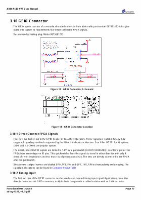
3.10 GPIO ConnectorThe GPIO option consists of a versatile shrouded connector from Molex with part number 0878331220 that giveusers with custom IO requirements four direct connect to FPGA signals.
Recommended mating plug: Molex 0875681273
Figure 13 : GPIO Connector Schematic
Figure 14 : GPIO Connector Location
3.10.1 Direct Connect FPGA Signals
Four nets are broken out to the GPIO header as two differential pairs. These signal are suitable for any 1.8Vsupported signaling standards supported by the Xilinx UltraScale architecture. See Xilinx UG571 for IO options.LVDS and 1.8 CMOS are popular options.
The direct connect GPIO signals are limited to 1.8V by a quickswitch (74CBTLVD3861BQ) in order to protect theFPGA from overvoltage on IO pins. This quickswitch allows the signals to travel in either direction with only 4ohms of series impedance and less than 1ns of propagation delay. The nets are directly connected to the FPGAafter the quickswitch.
Direct connect signal names are labeled GP0_1V8_P/N and GP1_1V8_P/N to show polarity and grouping. Thesignal pin allocations can be found in Complete Pinout Table
3.10.2 Timing Input
The first two pins of the GPIO connector can be used as an isolated timing input signal. Applications can eitherdirectly connect to the GPIO connector, or Alpha Data can provide a cabled solution with an SMA or similar
Page 17Functional Descriptionad-ug-1322_v2_5.pdf
ADM-PCIE-9V3 User Manual
connector on the front panel. Contact [email protected] for front panel connector options.
For pin locations, see signal name PPS_BUF_1V8 in Complete Pinout Table.
The signal is isolated through a optical isolator part number ACPL-M61L with a 739 ohm of series resistance.
3.11 User EEPROMA 2Kb I2C user EEPROM is provided for storing MAC addresses or other user information. The EEPROM is partnumber M24C02-RMC6TG.
The address pins A2, A1, and A0 are all strapped to a logical '0'.
Write protect (WP), Serial Clock (SCL), and Serial Data (SDA) pin assignments can be found in Complete PinoutTable with the names SPARE_WP, SPARE_SCL, and SPARE_SDA respectively.
WP, SDA, and SCL signals all have external pull-up resistors on the card.
Page 18 Functional Descriptionad-ug-1322_v2_5.pdf
ADM-PCIE-9V3 User Manual
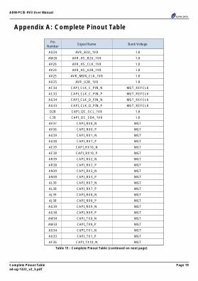
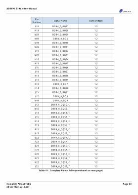
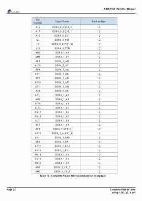
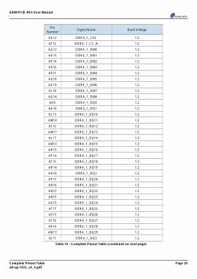
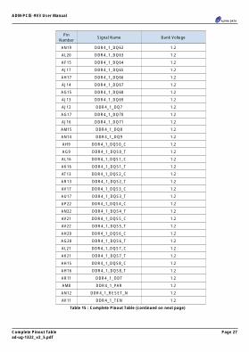
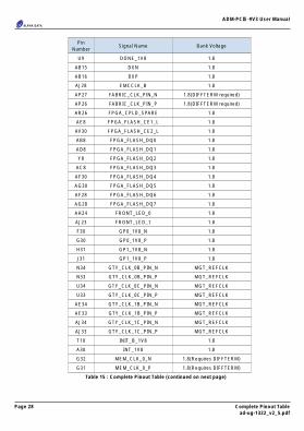
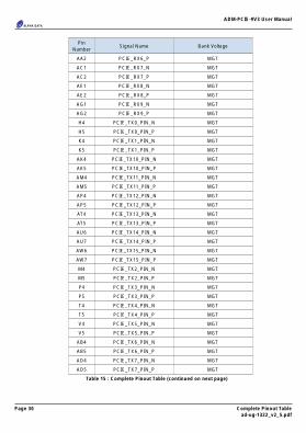
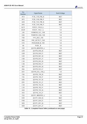
Appendix A: Complete Pinout Table
PinNumber Signal Name Bank Voltage
AU24 AVR_B2U_1V8 1.8
AW26 AVR_HS_B2U_1V8 1.8
AV26 AVR_HS_CLK_1V8 1.8
AV24 AVR_HS_U2B_1V8 1.8
AV25 AVR_MON_CLK_1V8 1.8
AU25 AVR_U2B_1V8 1.8
AC34 CAPI_CLK_C_PIN_N MGT_REFCLK
AC33 CAPI_CLK_C_PIN_P MGT_REFCLK
AG34 CAPI_CLK_D_PIN_N MGT_REFCLK
AG33 CAPI_CLK_D_PIN_P MGT_REFCLK
D28 CAPI_I2C_SCL_1V8 1.8
C28 CAPI_I2C_SDA_1V8 1.8
AV37 CAPI_RX0_N MGT
AV36 CAPI_RX0_P MGT
AU39 CAPI_RX1_N MGT
AU38 CAPI_RX1_P MGT
AE39 CAPI_RX10_N MGT
AE38 CAPI_RX10_P MGT
AR39 CAPI_RX2_N MGT
AR38 CAPI_RX2_P MGT
AN39 CAPI_RX3_N MGT
AN38 CAPI_RX3_P MGT
AL39 CAPI_RX7_N MGT
AL38 CAPI_RX7_P MGT
AJ39 CAPI_RX8_N MGT
AJ38 CAPI_RX8_P MGT
AG39 CAPI_RX9_N MGT
AG38 CAPI_RX9_P MGT
AW34 CAPI_TX0_N MGT
AW33 CAPI_TX0_P MGT
AU34 CAPI_TX1_N MGT
AU33 CAPI_TX1_P MGT
AF36 CAPI_TX10_N MGT
Table 15 : Complete Pinout Table (continued on next page)
Page 19Complete Pinout Tablead-ug-1322_v2_5.pdf
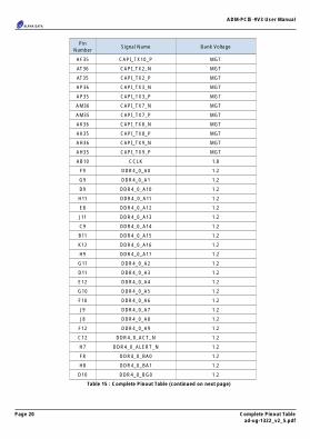
ADM-PCIE-9V3 User Manual
PinNumber Signal Name Bank Voltage
AF35 CAPI_TX10_P MGT
AT36 CAPI_TX2_N MGT
AT35 CAPI_TX2_P MGT
AP36 CAPI_TX3_N MGT
AP35 CAPI_TX3_P MGT
AM36 CAPI_TX7_N MGT
AM35 CAPI_TX7_P MGT
AK36 CAPI_TX8_N MGT
AK35 CAPI_TX8_P MGT
AH36 CAPI_TX9_N MGT
AH35 CAPI_TX9_P MGT
AB10 CCLK 1.8
F9 DDR4_0_A0 1.2
G9 DDR4_0_A1 1.2
D9 DDR4_0_A10 1.2
H11 DDR4_0_A11 1.2
E8 DDR4_0_A12 1.2
J11 DDR4_0_A13 1.2
C9 DDR4_0_A14 1.2
B11 DDR4_0_A15 1.2
K12 DDR4_0_A16 1.2
H9 DDR4_0_A17 1.2
G11 DDR4_0_A2 1.2
D11 DDR4_0_A3 1.2
E12 DDR4_0_A4 1.2
G10 DDR4_0_A5 1.2
F10 DDR4_0_A6 1.2
J9 DDR4_0_A7 1.2
J8 DDR4_0_A8 1.2
F12 DDR4_0_A9 1.2
C12 DDR4_0_ACT_N 1.2
H7 DDR4_0_ALERT_N 1.2
F8 DDR4_0_BA0 1.2
H8 DDR4_0_BA1 1.2
D10 DDR4_0_BG0 1.2
Table 15 : Complete Pinout Table (continued on next page)
Page 20 Complete Pinout Tablead-ug-1322_v2_5.pdf
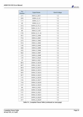
ADM-PCIE-9V3 User Manual
PinNumber Signal Name Bank Voltage
E11 DDR4_0_BG1 1.2
B10 DDR4_0_C0 1.2
C11 DDR4_0_C1 1.2
A9 DDR4_0_C2 1.2
G12 DDR4_0_CK_C 1.2
H12 DDR4_0_CK_T 1.2
B9 DDR4_0_CKE 1.2
E10 DDR4_0_CS_N 1.2
N12 DDR4_0_DM0 1.2
P14 DDR4_0_DM1 1.2
G15 DDR4_0_DM2 1.2
D14 DDR4_0_DM3 1.2
E20 DDR4_0_DM4 1.2
B20 DDR4_0_DM5 1.2
H22 DDR4_0_DM6 1.2
N22 DDR4_0_DM7 1.2
J13 DDR4_0_DM8 1.2
L10 DDR4_0_DQ0 1.2
L9 DDR4_0_DQ1 1.2
M15 DDR4_0_DQ10 1.2
M17 DDR4_0_DQ11 1.2
M14 DDR4_0_DQ12 1.2
N18 DDR4_0_DQ13 1.2
N16 DDR4_0_DQ14 1.2
N17 DDR4_0_DQ15 1.2
F15 DDR4_0_DQ16 1.2
E16 DDR4_0_DQ17 1.2
F14 DDR4_0_DQ18 1.2
E17 DDR4_0_DQ19 1.2
N9 DDR4_0_DQ2 1.2
G16 DDR4_0_DQ20 1.2
F17 DDR4_0_DQ21 1.2
E15 DDR4_0_DQ22 1.2
G17 DDR4_0_DQ23 1.2
A17 DDR4_0_DQ24 1.2
Table 15 : Complete Pinout Table (continued on next page)
Page 21Complete Pinout Tablead-ug-1322_v2_5.pdf
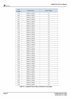
ADM-PCIE-9V3 User Manual
PinNumber Signal Name Bank Voltage
C16 DDR4_0_DQ25 1.2
B16 DDR4_0_DQ26 1.2
A14 DDR4_0_DQ27 1.2
B17 DDR4_0_DQ28 1.2
B14 DDR4_0_DQ29 1.2
M9 DDR4_0_DQ3 1.2
D16 DDR4_0_DQ30 1.2
D15 DDR4_0_DQ31 1.2
F18 DDR4_0_DQ32 1.2
F20 DDR4_0_DQ33 1.2
F19 DDR4_0_DQ34 1.2
D21 DDR4_0_DQ35 1.2
E18 DDR4_0_DQ36 1.2
G19 DDR4_0_DQ37 1.2
E21 DDR4_0_DQ38 1.2
G20 DDR4_0_DQ39 1.2
M10 DDR4_0_DQ4 1.2
D18 DDR4_0_DQ40 1.2
B22 DDR4_0_DQ41 1.2
A19 DDR4_0_DQ42 1.2
A18 DDR4_0_DQ43 1.2
C19 DDR4_0_DQ44 1.2
B19 DDR4_0_DQ45 1.2
A22 DDR4_0_DQ46 1.2
C18 DDR4_0_DQ47 1.2
G22 DDR4_0_DQ48 1.2
J20 DDR4_0_DQ49 1.2
K11 DDR4_0_DQ5 1.2
H19 DDR4_0_DQ50 1.2
J19 DDR4_0_DQ51 1.2
H18 DDR4_0_DQ52 1.2
J18 DDR4_0_DQ53 1.2
G21 DDR4_0_DQ54 1.2
K18 DDR4_0_DQ55 1.2
L20 DDR4_0_DQ56 1.2
Table 15 : Complete Pinout Table (continued on next page)
Page 22 Complete Pinout Tablead-ug-1322_v2_5.pdf
ADM-PCIE-9V3 User Manual
PinNumber Signal Name Bank Voltage
L18 DDR4_0_DQ57 1.2
N19 DDR4_0_DQ58 1.2
M21 DDR4_0_DQ59 1.2
M11 DDR4_0_DQ6 1.2
M19 DDR4_0_DQ60 1.2
M22 DDR4_0_DQ61 1.2
L19 DDR4_0_DQ62 1.2
M20 DDR4_0_DQ63 1.2
H16 DDR4_0_DQ64 1.2
K15 DDR4_0_DQ65 1.2
J16 DDR4_0_DQ66 1.2
J14 DDR4_0_DQ67 1.2
K13 DDR4_0_DQ68 1.2
L13 DDR4_0_DQ69 1.2
K10 DDR4_0_DQ7 1.2
H14 DDR4_0_DQ70 1.2
J15 DDR4_0_DQ71 1.2
L17 DDR4_0_DQ8 1.2
M16 DDR4_0_DQ9 1.2
L12 DDR4_0_DQS0_C 1.2
M12 DDR4_0_DQS0_T 1.2
L14 DDR4_0_DQS1_C 1.2
L15 DDR4_0_DQS1_T 1.2
E13 DDR4_0_DQS2_C 1.2
F13 DDR4_0_DQS2_T 1.2
A15 DDR4_0_DQS3_C 1.2
B15 DDR4_0_DQS3_T 1.2
E22 DDR4_0_DQS4_C 1.2
F22 DDR4_0_DQS4_T 1.2
B21 DDR4_0_DQS5_C 1.2
C21 DDR4_0_DQS5_T 1.2
K20 DDR4_0_DQS6_C 1.2
K21 DDR4_0_DQS6_T 1.2
K22 DDR4_0_DQS7_C 1.2
L22 DDR4_0_DQS7_T 1.2
Table 15 : Complete Pinout Table (continued on next page)
Page 23Complete Pinout Tablead-ug-1322_v2_5.pdf
ADM-PCIE-9V3 User Manual
PinNumber Signal Name Bank Voltage
K16 DDR4_0_DQS8_C 1.2
K17 DDR4_0_DQS8_T 1.2
A10 DDR4_0_ODT 1.2
G7 DDR4_0_PAR 1.2
F7 DDR4_0_RESET_N 1.2
J10 DDR4_0_TEN 1.2
AN9 DDR4_1_A0 1.2
AM9 DDR4_1_A1 1.2
AR8 DDR4_1_A10 1.2
AL10 DDR4_1_A11 1.2
AP8 DDR4_1_A12 1.2
AK11 DDR4_1_A13 1.2
AP9 DDR4_1_A14 1.2
AV10 DDR4_1_A15 1.2
AT11 DDR4_1_A16 1.2
AL8 DDR4_1_A17 1.2
AP11 DDR4_1_A2 1.2
AU9 DDR4_1_A3 1.2
AT10 DDR4_1_A4 1.2
AL12 DDR4_1_A5 1.2
AM12 DDR4_1_A6 1.2
AM10 DDR4_1_A7 1.2
AL11 DDR4_1_A8 1.2
AP7 DDR4_1_A9 1.2
AV9 DDR4_1_ACT_N 1.2
AR10 DDR4_1_ALERT_N 1.2
AN11 DDR4_1_BA0 1.2
AR9 DDR4_1_BA1 1.2
AP12 DDR4_1_BG0 1.2
AN10 DDR4_1_BG1 1.2
AW13 DDR4_1_C0 1.2
AU10 DDR4_1_C1 1.2
AW11 DDR4_1_C2 1.2
AN7 DDR4_1_CK_C 1.2
AM7 DDR4_1_CK_T 1.2
Table 15 : Complete Pinout Table (continued on next page)
Page 24 Complete Pinout Tablead-ug-1322_v2_5.pdf
ADM-PCIE-9V3 User Manual
PinNumber Signal Name Bank Voltage
AU12 DDR4_1_CKE 1.2
AT12 DDR4_1_CS_N 1.2
AG12 DDR4_1_DM0 1.2
AK15 DDR4_1_DM1 1.2
AP16 DDR4_1_DM2 1.2
AV16 DDR4_1_DM3 1.2
AP21 DDR4_1_DM4 1.2
AU20 DDR4_1_DM5 1.2
AG19 DDR4_1_DM6 1.2
AL18 DDR4_1_DM7 1.2
AG14 DDR4_1_DM8 1.2
AK9 DDR4_1_DQ0 1.2
AK10 DDR4_1_DQ1 1.2
AL13 DDR4_1_DQ10 1.2
AM14 DDR4_1_DQ11 1.2
AL15 DDR4_1_DQ12 1.2
AM17 DDR4_1_DQ13 1.2
AL17 DDR4_1_DQ14 1.2
AM13 DDR4_1_DQ15 1.2
AR15 DDR4_1_DQ16 1.2
AP14 DDR4_1_DQ17 1.2
AT15 DDR4_1_DQ18 1.2
AR14 DDR4_1_DQ19 1.2
AH10 DDR4_1_DQ2 1.2
AP17 DDR4_1_DQ20 1.2
AN16 DDR4_1_DQ21 1.2
AN17 DDR4_1_DQ22 1.2
AN15 DDR4_1_DQ23 1.2
AU15 DDR4_1_DQ24 1.2
AT17 DDR4_1_DQ25 1.2
AV15 DDR4_1_DQ26 1.2
AT16 DDR4_1_DQ27 1.2
AV14 DDR4_1_DQ28 1.2
AW17 DDR4_1_DQ29 1.2
AJ11 DDR4_1_DQ3 1.2
Table 15 : Complete Pinout Table (continued on next page)
Page 25Complete Pinout Tablead-ug-1322_v2_5.pdf

ADM-PCIE-9V3 User Manual
PinNumber Signal Name Bank Voltage
AW14 DDR4_1_DQ30 1.2
AW18 DDR4_1_DQ31 1.2
AP19 DDR4_1_DQ32 1.2
AT20 DDR4_1_DQ33 1.2
AN21 DDR4_1_DQ34 1.2
AR19 DDR4_1_DQ35 1.2
AN20 DDR4_1_DQ36 1.2
AR18 DDR4_1_DQ37 1.2
AR20 DDR4_1_DQ38 1.2
AP18 DDR4_1_DQ39 1.2
AJ9 DDR4_1_DQ4 1.2
AW19 DDR4_1_DQ40 1.2
AU22 DDR4_1_DQ41 1.2
AV19 DDR4_1_DQ42 1.2
AW22 DDR4_1_DQ43 1.2
AU18 DDR4_1_DQ44 1.2
AT22 DDR4_1_DQ45 1.2
AW21 DDR4_1_DQ46 1.2
AU19 DDR4_1_DQ47 1.2
AH19 DDR4_1_DQ48 1.2
AJ22 DDR4_1_DQ49 1.2
AH12 DDR4_1_DQ5 1.2
AF21 DDR4_1_DQ50 1.2
AH22 DDR4_1_DQ51 1.2
AF20 DDR4_1_DQ52 1.2
AJ19 DDR4_1_DQ53 1.2
AH21 DDR4_1_DQ54 1.2
AJ21 DDR4_1_DQ55 1.2
AM19 DDR4_1_DQ56 1.2
AK20 DDR4_1_DQ57 1.2
AM22 DDR4_1_DQ58 1.2
AL22 DDR4_1_DQ59 1.2
AG10 DDR4_1_DQ6 1.2
AM20 DDR4_1_DQ60 1.2
AK19 DDR4_1_DQ61 1.2
Table 15 : Complete Pinout Table (continued on next page)
Page 26 Complete Pinout Tablead-ug-1322_v2_5.pdf
ADM-PCIE-9V3 User Manual
PinNumber Signal Name Bank Voltage
AN19 DDR4_1_DQ62 1.2
AL20 DDR4_1_DQ63 1.2
AF15 DDR4_1_DQ64 1.2
AJ17 DDR4_1_DQ65 1.2
AH17 DDR4_1_DQ66 1.2
AJ14 DDR4_1_DQ67 1.2
AG15 DDR4_1_DQ68 1.2
AJ13 DDR4_1_DQ69 1.2
AJ12 DDR4_1_DQ7 1.2
AG17 DDR4_1_DQ70 1.2
AJ16 DDR4_1_DQ71 1.2
AM15 DDR4_1_DQ8 1.2
AN14 DDR4_1_DQ9 1.2
AH9 DDR4_1_DQS0_C 1.2
AG9 DDR4_1_DQS0_T 1.2
AL16 DDR4_1_DQS1_C 1.2
AK16 DDR4_1_DQS1_T 1.2
AT13 DDR4_1_DQS2_C 1.2
AR13 DDR4_1_DQS2_T 1.2
AV17 DDR4_1_DQS3_C 1.2
AU17 DDR4_1_DQS3_T 1.2
AP22 DDR4_1_DQS4_C 1.2
AN22 DDR4_1_DQS4_T 1.2
AV21 DDR4_1_DQS5_C 1.2
AV22 DDR4_1_DQS5_T 1.2
AH20 DDR4_1_DQS6_C 1.2
AG20 DDR4_1_DQS6_T 1.2
AL21 DDR4_1_DQS7_C 1.2
AK21 DDR4_1_DQS7_T 1.2
AH15 DDR4_1_DQS8_C 1.2
AH16 DDR4_1_DQS8_T 1.2
AR11 DDR4_1_ODT 1.2
AM8 DDR4_1_PAR 1.2
AN12 DDR4_1_RESET_N 1.2
AV11 DDR4_1_TEN 1.2
Table 15 : Complete Pinout Table (continued on next page)
Page 27Complete Pinout Tablead-ug-1322_v2_5.pdf
ADM-PCIE-9V3 User Manual
PinNumber Signal Name Bank Voltage
U9 DONE_1V8 1.8
AB15 DXN 1.8
AB16 DXP 1.8
AJ28 EMCCLK_B 1.8
AP27 FABRIC_CLK_PIN_N 1.8(DIFFTERM required)
AP26 FABRIC_CLK_PIN_P 1.8(DIFFTERM required)
AR26 FPGA_CPLD_SPARE 1.8
AE8 FPGA_FLASH_CE1_L 1.8
AV30 FPGA_FLASH_CE2_L 1.8
AB8 FPGA_FLASH_DQ0 1.8
AD8 FPGA_FLASH_DQ1 1.8
Y8 FPGA_FLASH_DQ2 1.8
AC8 FPGA_FLASH_DQ3 1.8
AF30 FPGA_FLASH_DQ4 1.8
AG30 FPGA_FLASH_DQ5 1.8
AF28 FPGA_FLASH_DQ6 1.8
AG28 FPGA_FLASH_DQ7 1.8
AH24 FRONT_LED_0 1.8
AJ23 FRONT_LED_1 1.8
F30 GP0_1V8_N 1.8
G30 GP0_1V8_P 1.8
H31 GP1_1V8_N 1.8
J31 GP1_1V8_P 1.8
N34 GTY_CLK_0B_PIN_N MGT_REFCLK
N33 GTY_CLK_0B_PIN_P MGT_REFCLK
U34 GTY_CLK_0C_PIN_N MGT_REFCLK
U33 GTY_CLK_0C_PIN_P MGT_REFCLK
AE34 GTY_CLK_1B_PIN_N MGT_REFCLK
AE33 GTY_CLK_1B_PIN_P MGT_REFCLK
AJ34 GTY_CLK_1C_PIN_N MGT_REFCLK
AJ33 GTY_CLK_1C_PIN_P MGT_REFCLK
T10 INIT_B_1V8 1.8
A30 INT_1V8 1.8
G32 MEM_CLK_0_N 1.8(Requires DIFFTERM)
G31 MEM_CLK_0_P 1.8(Requires DIFFTERM)
Table 15 : Complete Pinout Table (continued on next page)
Page 28 Complete Pinout Tablead-ug-1322_v2_5.pdf

ADM-PCIE-9V3 User Manual
PinNumber Signal Name Bank Voltage
AN26 MEM_CLK_1_PIN_N 1.8(Requires DIFFTERM)
AN25 MEM_CLK_1_PIN_P 1.8(Requires DIFFTERM)
C29 OPTICAL_INT_1V8_L 1.8
B29 OPTICAL_RESET_1V8_L 1.8
A28 OPTICAL_SCL_1V8 1.8
A29 OPTICAL_SDA_1V8 1.8
AA6 PCIE_REFCLK_1_PIN_N MGT_REFCLK
AA7 PCIE_REFCLK_1_PIN_P MGT_REFCLK
AJ6 PCIE_REFCLK_2_PIN_N MGT_REFCLK
AJ7 PCIE_REFCLK_2_PIN_P MGT_REFCLK
J1 PCIE_RX0_N MGT
J2 PCIE_RX0_P MGT
L1 PCIE_RX1_N MGT
L2 PCIE_RX1_P MGT
AJ1 PCIE_RX10_N MGT
AJ2 PCIE_RX10_P MGT
AL1 PCIE_RX11_N MGT
AL2 PCIE_RX11_P MGT
AN1 PCIE_RX12_N MGT
AN2 PCIE_RX12_P MGT
AR1 PCIE_RX13_N MGT
AR2 PCIE_RX13_P MGT
AU1 PCIE_RX14_N MGT
AU2 PCIE_RX14_P MGT
AV3 PCIE_RX15_N MGT
AV4 PCIE_RX15_P MGT
N1 PCIE_RX2_N MGT
N2 PCIE_RX2_P MGT
R1 PCIE_RX3_N MGT
R2 PCIE_RX3_P MGT
U1 PCIE_RX4_N MGT
U2 PCIE_RX4_P MGT
W1 PCIE_RX5_N MGT
W2 PCIE_RX5_P MGT
AA1 PCIE_RX6_N MGT
Table 15 : Complete Pinout Table (continued on next page)
Page 29Complete Pinout Tablead-ug-1322_v2_5.pdf
ADM-PCIE-9V3 User Manual
PinNumber Signal Name Bank Voltage
AA2 PCIE_RX6_P MGT
AC1 PCIE_RX7_N MGT
AC2 PCIE_RX7_P MGT
AE1 PCIE_RX8_N MGT
AE2 PCIE_RX8_P MGT
AG1 PCIE_RX9_N MGT
AG2 PCIE_RX9_P MGT
H4 PCIE_TX0_PIN_N MGT
H5 PCIE_TX0_PIN_P MGT
K4 PCIE_TX1_PIN_N MGT
K5 PCIE_TX1_PIN_P MGT
AK4 PCIE_TX10_PIN_N MGT
AK5 PCIE_TX10_PIN_P MGT
AM4 PCIE_TX11_PIN_N MGT
AM5 PCIE_TX11_PIN_P MGT
AP4 PCIE_TX12_PIN_N MGT
AP5 PCIE_TX12_PIN_P MGT
AT4 PCIE_TX13_PIN_N MGT
AT5 PCIE_TX13_PIN_P MGT
AU6 PCIE_TX14_PIN_N MGT
AU7 PCIE_TX14_PIN_P MGT
AW6 PCIE_TX15_PIN_N MGT
AW7 PCIE_TX15_PIN_P MGT
M4 PCIE_TX2_PIN_N MGT
M5 PCIE_TX2_PIN_P MGT
P4 PCIE_TX3_PIN_N MGT
P5 PCIE_TX3_PIN_P MGT
T4 PCIE_TX4_PIN_N MGT
T5 PCIE_TX4_PIN_P MGT
V4 PCIE_TX5_PIN_N MGT
V5 PCIE_TX5_PIN_P MGT
AB4 PCIE_TX6_PIN_N MGT
AB5 PCIE_TX6_PIN_P MGT
AD4 PCIE_TX7_PIN_N MGT
AD5 PCIE_TX7_PIN_P MGT
Table 15 : Complete Pinout Table (continued on next page)
Page 30 Complete Pinout Tablead-ug-1322_v2_5.pdf
ADM-PCIE-9V3 User Manual
PinNumber Signal Name Bank Voltage
AF4 PCIE_TX8_PIN_N MGT
AF5 PCIE_TX8_PIN_P MGT
AH4 PCIE_TX9_PIN_N MGT
AH5 PCIE_TX9_PIN_P MGT
AJ31 PERST_1V8_0_L 1.8
AH29 PERST_1V8_1_L 1.8
J30 POWER9_SCL_1V8 1.8
K30 POWER9_SDA_1V8 1.8
P30 PPS_BUF_1V8 1.8
B30 PRE_DETECT_1V8 1.8
V10 PROGRAM_B_1V8 1.8
U8 PUDC_B 1.8
F29 QSFP0_MODPRS_L 1.8
G39 QSFP0_RX0_N MGT
G38 QSFP0_RX0_P MGT
E39 QSFP0_RX1_N MGT
E38 QSFP0_RX1_P MGT
C39 QSFP0_RX2_N MGT
C38 QSFP0_RX2_P MGT
B37 QSFP0_RX3_N MGT
B36 QSFP0_RX3_P MGT
D31 QSFP0_SEL_1V8_L 1.8
F36 QSFP0_TX0_N MGT
F35 QSFP0_TX0_P MGT
D36 QSFP0_TX1_N MGT
D35 QSFP0_TX1_P MGT
C34 QSFP0_TX2_N MGT
C33 QSFP0_TX2_P MGT
A34 QSFP0_TX3_N MGT
A33 QSFP0_TX3_P MGT
F33 QSFP1_MODPRS_L 1.8
R39 QSFP1_RX0_N MGT
R38 QSFP1_RX0_P MGT
N39 QSFP1_RX1_N MGT
N38 QSFP1_RX1_P MGT
Table 15 : Complete Pinout Table (continued on next page)
Page 31Complete Pinout Tablead-ug-1322_v2_5.pdf

ADM-PCIE-9V3 User Manual
PinNumber Signal Name Bank Voltage
L39 QSFP1_RX2_N MGT
L38 QSFP1_RX2_P MGT
J39 QSFP1_RX3_N MGT
J38 QSFP1_RX3_P MGT
D30 QSFP1_SEL_1V8_L 1.8
P36 QSFP1_TX0_N MGT
P35 QSFP1_TX0_P MGT
M36 QSFP1_TX1_N MGT
M35 QSFP1_TX1_P MGT
K36 QSFP1_TX2_N MGT
K35 QSFP1_TX2_P MGT
H36 QSFP1_TX3_N MGT
H35 QSFP1_TX3_P MGT
R6 REFCLK100_PIN_N MGT
R7 REFCLK100_PIN_P MGT
L30 SI5328_1V8_SCL 1.8
L29 SI5328_1V8_SDA 1.8
M30 SI5328_REFCLK_IN_N 1.8 (LVDS)
M29 SI5328_REFCLK_IN_P 1.8(LVDS)
L34 SI5328_REFCLK_OUT0_PIN_N MGT_REFCLK
L33 SI5328_REFCLK_OUT0_PIN_P MGT_REFCLK
R34 SI5328_REFCLK_OUT1_PIN_N MGT_REFCLK
R33 SI5328_REFCLK_OUT1_PIN_P MGT_REFCLK
AT25 SPARE_SCL 1.8
AT26 SPARE_SDA 1.8
AP23 SPARE_WP 1.8
AW24 SRVC_MD_L_1V8 1.8
Y10 TCK 1.8
AC9 TDI 1.8
Y9 TDO 1.8
AD10 TMS 1.8
AT27 USER_LED_G0 1.8
AU27 USER_LED_G1 1.8
AU23 USER_LED_R 1.8
AV27 USR_SW0 1.8
Table 15 : Complete Pinout Table (continued on next page)
Page 32 Complete Pinout Tablead-ug-1322_v2_5.pdf
ADM-PCIE-9V3 User Manual
PinNumber Signal Name Bank Voltage
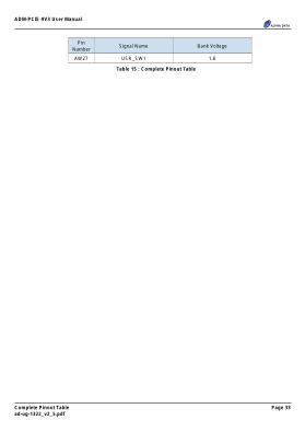
AW27 USR_SW1 1.8
Table 15 : Complete Pinout Table
Page 33Complete Pinout Tablead-ug-1322_v2_5.pdf
ADM-PCIE-9V3 User Manual
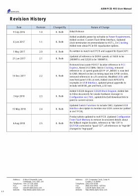
Revision HistoryDate Revision Changed By Nature of Change
9 Sep 2016 1.0 K. Roth Initial Release
6 Jan 2017 1.1 K. Roth
Added available power by rail table to Power Requirements,Added section: Custom Flash Write Interface, Updatedclock termination recommendation to HSTL_I in Clocking,Added note about PCIe RX equalization options.
1 May 2017 2.0 K. Roth Re-written to match rev3 PCB and support for OpenCAPI
21 Jun 2017 2.1 K. RothUpdated all reference to DDR4 speeds at 16GB to be2400MT/s and 32GB to be 1866MT/s.
14 Dec 2017 2.2 K. Roth
Removed inaccurate PERST location reference in PCIExpress, Noted 312.5MHz limit in Clocking, removedreference to -2i speed grade,QSFP LP_MODE is now tiedto GND, Moved section on timing input into GPIO section,removed references to u.fl connector, Modified LEDs withnew front panel LEDs at rev6, Added clock AVR2UTILexamples in USB Interface, updated pinout appendix toinclude refclk100_pin and front_LED nets
3 Apr 2018 2.3 K. Roth
Added Si5328 diagram Si5328 Block Diagram, Added linkto Xilinx documents for vivado hardware manager inConfiguration via JTAG, updated Avr2util download link topoint to current version.
15 May 2018 2.4 K. RothUpdated Switch Functions to include SW2, Updated USBInterface description to mention rear USB connector (addedin rev7 PCB).
6 Aug 2018 2.5 K. Roth
Product photo updated to rev8 PCB ,Updated ConfigurationFrom Flash Memory to remove inconsistent details aboutthe fallback region location, reference to "tile 129" inQSFP28 corrected to "quad 127", all references to "mgt tile"changed to "mgt quad".
Address: 4 West Silvermills LaneEdinburgh, EH3 5BD, UK
Telephone: +44 131 558 2600Fax: +44 131 558 2700email: [email protected]: http://www.alpha-data.com
Address: 611 Corporate Circle, Suite HGolden, CO 80401
Telephone: (303) 954 8768Fax: (866) 820 9956 - toll freeemail: [email protected]: http://www.alpha-data.com
4.9