Embed Size (px)
Citation preview

8/10/2019 AD524
http://slidepdf.com/reader/full/ad524 1/28

8/10/2019 AD524
http://slidepdf.com/reader/full/ad524 2/28
AD524
Rev. F | Page 2 of 28
TABLE OF CONTENTSFeatures .............................................................................................. 1
Functional Block Diagram .............................................................. 1
General Description ......................................................................... 1
Product Highlights ........................................................................... 1 Revision History ............................................................................... 2
Specifications ..................................................................................... 3
Absolute Maximum Ratings ............................................................ 8
Connection Diagrams .................................................................. 8
ESD Caution .................................................................................. 8
Typical Performance Characteristics ............................................. 9
Test Circuits ................................................................................. 14
Theory of Operation ...................................................................... 15
Input Protection .......................................................................... 15
Input Offset and Output Offset ................................................ 15
Gain .............................................................................................. 16
Input Bias Currents .................................................................... 17
Common-Mode Rejection ........................................................ 17 Grounding ................................................................................... 18
Sense Terminal............................................................................ 18
Reference Terminal .................................................................... 18
Programmable Gain ................................................................... 20
Autozero Circuits ....................................................................... 20
Error Budget Analysis ................................................................ 21
Outline Dimensions ....................................................................... 24
Ordering Guide .......................................................................... 25
REVISION HISTORY
11/07—Rev. E to Rev. F Updated Format .................................................................. UniversalChanges to General Description .................................................... 1Changes to Figure 1 .......................................................................... 1Changes to Figure 3 and Figure 4 Captions .................................. 8Changes to Error Budget Analysis Section ................................. 21Changes to Ordering Guide .......................................................... 25
4/99—Rev. D to Rev. E
8/10/2019 AD524
http://slidepdf.com/reader/full/ad524 3/28
AD524
Rev. F | Page 3 of 28
SPECIFICATIONS
@ VS = ±15 V, R L = 2 kΩ and TA = +25°C, unless otherwise noted.
All min and max specifications are guaranteed. Specifications shown in boldface are tested on all production units at the final electricaltest. Results from those tests are used to calculate outgoing quality levels.
Table 1.
AD524A AD524B
Parameter Min Typ Max Min Typ Max Unit
GAIN
Gain Equation (External Resistor Gain Programming)
%201000,40
±⎥⎦
⎤⎢⎣
⎡+
GR %201
000,40±⎥
⎦
⎤⎢⎣
⎡+
GR
Gain Range (Pin Programmable) 1 to 1000 1 to 1000
Gain Error1
G = 1 ±0.05 ±0.03 %
G = 10 ±0.25 ±0.15 %
G = 100 ±0.5 ±0.35 %
G = 1000 ±2.0 ±1.0 %Nonlinearity
G = 1 ±0.01 ±0.005 %G = 10, G = 100 ±0.01 ±0.005 %
G = 1000 ±0.01 ±0.01 %
Gain vs. Temperature
G = 1 5 5 ppm/°CG = 10 15 10 ppm/°C
G = 100 35 25 ppm/°C
G = 1000 100 50 ppm/°C
VOLTAGE OFFSET (May be Nulled)
Input Offset Voltage 250 100 µV
vs. Temperature 2 0.75 µV/°COutput Offset Voltage 5 3 mV
vs. Temperature 100 50 µV
Offset Referred to the Input vs. Supply
G = 1 70 75 dB
G = 10 85 95 dB
G = 100 95 105 dB
G = 1000 100 110 dB
INPUT CURRENT
Input Bias Current ±50 ±25 nA
vs. Temperature ±100 ±100 pA/°CInput Offset Current ±35 ±15 nA
vs. Temperature ±100 ±100 pA/°C

8/10/2019 AD524
http://slidepdf.com/reader/full/ad524 4/28
AD524
Rev. F | Page 4 of 28
AD524A AD524B
Parameter Min Typ Max Min Typ Max Unit
INPUT
Input Impedance
Differential Resistance 109 109 Ω
Differential Capacitance 10 10 pFCommon-Mode Resistance 109 109 Ω
Common-Mode Capacitance 10 10 pF
Input Voltage Range
Maximum Differential Input Linear (VDL)2 ±10 ±10 V
Maximum Common-Mode Linear (VCM)2
⎟ ⎠
⎞⎜⎝
⎛ ×− DV
2
GV12 ⎟
⎠
⎞⎜⎝
⎛ ×− DV
2
GV12
V
Common-Mode Rejection DC to 60 Hz with 1 kΩ Source Imbalance V
G = 1 70 75 dB
G = 10 90 95 dB
G = 100 100 105 dB
G = 1000 110 115 dB
OUTPUT RATINGVOUT, RL = 2 kΩ ±10 ±10 V
DYNAMIC RESPONSESmall Signal – 3 dB
G = 1 1 1 MHz
G = 10 400 400 kHz
G = 100 150 150 kHzG = 1000 25 25 kHz
Slew Rate 5.0 5.0 V/µs
Settling Time to 0.01%, 20 V Step
G = 1 to 100 15 15 µsG = 1000 75 75 µs
NOISE
Voltage Noise, 1 kHzRTI 7 7 nV/√Hz
RTO 90 90 nV√Hz
RTI, 0.1 Hz to 10 HzG = 1 15 15 µV p-p
G = 10 2 2 µV p-p
G = 100, 1000 0.3 0.3 µV p-p
Current Noise
0.1 Hz to 10 Hz 60 60 pA p-p
SENSE INPUT
RIN 20 20 kΩ ± 20%IIN 15 15 µA
Voltage Range ±10 ±10 VGain to Output 1 1 %
REFERENCE INPUTRIN 40 40 kΩ ± 20%
IIN 15 15 µA
Voltage Range ±10 ±10 V
Gain to Output 1 1 %

8/10/2019 AD524
http://slidepdf.com/reader/full/ad524 5/28
AD524
Rev. F | Page 5 of 28
AD524A AD524B
Parameter Min Typ Max Min Typ Max Unit
TEMPERATURE RANGE
Specified Performance –25 +85 –25 +85 °C
Storage –65 +150 –65 +150 °C
POWER SUPPLYPower Supply Range ±6 ±15 ±18 ±6 ±15 ±18 V
Quiescent Current 3.5 5.0 3.5 5.0 mA
1 Does not include effects of external resistor, RG.2 VOL is the maximum differential input voltage at G = 1 for specified nonlinearity.
VDL at the maximum = 10 V/G.VD = actual differential input voltage.Example: G = 10, VD = 0.50.VCM = 12 V − (10/2 × 0.50 V) = 9.5 V.
@ VS = ±15 V, R L = 2 kΩ and TA = +25°C, unless otherwise noted.
All min and max specifications are guaranteed. Specifications shown in boldface are tested on all production units at the final electricaltest. Results from those tests are used to calculate outgoing quality levels.
Table 2.
AD524C AD524S
Parameter Min Typ Max Min Typ Max Unit
GAIN
Gain Equation (External Resistor Gain Programming)
%201000,40
±⎥⎦
⎤⎢⎣
⎡+
GR %201
000,40±⎥
⎦
⎤⎢⎣
⎡+
GR
Gain Range (Pin Programmable) 1 to 1000 1 to 1000
Gain Error1
G = 1 ±0.02 ±0.05 %
G = 10 ±0.1 ±0.25 %
G = 100 ±0.25 ±0.5 %
G = 1000 ±0.5 ±2.0 %Nonlinearity
G = 1 ±0.003 ±0.01 %G = 10, G = 100 ±0.003 ±0.01 %
G = 1000 ±0.01 ±0.01 %
Gain vs. Temperature
G = 1 5 5 ppm/°CG = 10 10 10 ppm/°C
G = 100 25 25 ppm/°C
G = 1000 50 50 ppm/°C
VOLTAGE OFFSET (May be Nulled)
Input Offset Voltage 50 100 µV
vs. Temperature 0.5 2.0 µV/°COutput Offset Voltage 2.0 3.0 mV
vs. Temperature 25 50 µV
Offset Referred to the Input vs. Supply
G = 1 80 75 dB
G = 10 100 95 dB
G = 100 110 105 dB
G = 1000 115 110 dB
8/10/2019 AD524
http://slidepdf.com/reader/full/ad524 6/28

8/10/2019 AD524
http://slidepdf.com/reader/full/ad524 7/28
AD524
Rev. F | Page 7 of 28
AD524C AD524S
Parameter Min Typ Max Min Typ Max Unit
REFERENCE INPUT
RIN 40 40 kΩ ± 20%
IIN 15 15 µA
Voltage Range 10 10 VGain to Output 1 1 %
TEMPERATURE RANGESpecified Performance –25 +85 –55 +85 °C
Storage –65 +150 –65 +150 °C
POWER SUPPLY
Power Supply Range ±6 ±15 ±18 ±6 ±15 ±18 V
Quiescent Current 3.5 5.0 3.5 5.0 mA
1 Does not include effects of external resistor RG.2 VOL is the maximum differential input voltage at G = 1 for specified nonlinearity.
VDL at the maximum = 10 V/G.VD = actual differential input voltage.Example: G = 10, VD = 0.50.VCM = 12 V − (10/2 × 0.50 V) = 9.5 V.

8/10/2019 AD524
http://slidepdf.com/reader/full/ad524 8/28
AD524
Rev. F | Page 8 of 28
ABSOLUTE MAXIMUM RATINGS
Table 3.
Parameter Rating
Supply Voltage ±18 V
Internal Power Dissipation 450 mWInput Voltage1
(Either Input Simultaneously) |VIN| + |VS| <36 V
Output Short-Circuit Duration Indefinite
Storage Temperature Range
(R) –65°C to +125°C(D, E) –65°C to +150°C
Operating Temperature Range
AD524A/AD524B/AD524C –25°C to +85°C
AD524S –55°C to +125°CLead Temperature (Soldering, 60 sec) +300°C
1 Maximum input voltage specification refers to maximum voltage to whicheither input terminal may be raised with or without device power applied.For example, with ±18 volt supplies maximum, V IN is ±18 V; with zero supplyvoltage maximum, VIN is ±36 V.
Stresses above those listed under Absolute Maximum Ratingsmay cause permanent damage to the device. This is a stressrating only; functional operation of the device at these or anyother conditions above those indicated in the operationalsection of this specification is not implied. Exposure to absolutemaximum rating conditions for extended periods may affectdevice reliability.
RG1 16
–INPUT1
+INPUT2
RG2
3
4INPUTNULL
5INPUTNULL
6REFERENCE
9OUTPUT
8 +VS
7 –VS
SENSE10G = 1000
11G = 100
12G = 10
13
OUTPUTNULL
14
OUTPUTNULL
15
0.170 (4.33)
0.103(2.61)
PAD NUMBERS CORRESPOND TO PIN NUMBERS FORTHE D-16 AND RW-16 16-LEAD CERAMIC PACKAGES.
0 0 5 0 0 - 0 0 2
Figure 2. Metallization PhotographContact factory for latest dimensions;
Dimensions shown in inches and (mm)
CONNECTION DIAGRAMS
16
15
14
13
12
11
10
9
1
2
3
4
5
6
7
8
– INPUT
+ INPUT
INPUT NULL
INPUT NULL
REFERENCE
OUTPUT NULL
OUTPUT NULLG = 10
G = 100
G = 1000
SENSE
OUTPUT
AD524
RG2
RG1
–VS
–VS
+VS
+VS
SHORT TO
RG2 FOR
DESIRED
GAIN
4 15
5 14 OUTPUTOFFSET NULL
INPUTOFFSET NULL
TOP VIEW(Not to Scale)
0 0 5 0 0 - 0 0 3
Figure 3. Ceramic (D) andSOIC (RW-16 and D-16) Packages
SHORT TO
RG2 FOR
DESIRED
GAIN
4RG2
5INPUT NULL
6NC
7INPUT NULL
8REFERENCE
18 OUTPUT NULL
17 G = 10
16 NC
15 G = 100
14 G = 1000
19 R G 1
20 O U T P U
T
N U L L
1 N C
2 – I N P U T
3 + I N P U T
13
S E N S E
12
O U T P U T
11
N C
10
+ V S
9
– V S
NC = NO CONNECT
AD524TOP VIEW
(Not to Scale)
+VS –VS
INPUTOFFSET NULL
OUTPUTOFFSET NULL
7 19
5 18
0 0 5 0 0 - 0
0 4
Figure 4. Leadless Chip Carrier (E)
ESD CAUTION

8/10/2019 AD524
http://slidepdf.com/reader/full/ad524 9/28
AD524
Rev. F | Page 9 of 28
TYPICAL PERFORMANCE CHARACTERISTICS
20
15
10
5
00 5 10 15 20
SUPPLY VOLTAGE (±V)
I N P U T V O L T A G E ( ± V )
+25°C
0 0 5 0 0 - 0 0 5
Figure 5. Input Voltage Range vs. Supply Voltage, G = 1
20
15
10
5
00 5 10 15 20
SUPPLY VOLTAGE (±V)
O U T P U T V O L T A G E S W I N G ( ± V )
0 0 5 0 0
- 0 0 6
Figure 6. Output Voltage Swing vs. Supply Voltage
30
20
10
010 100 1k 10k
LOAD RESISTANCE (Ω)
O U T P U T V O L T A G E
S W I N G ( V p - p )
0 0 5 0 0 - 0 0 7
Figure 7. Output Voltage Swing vs. Load Resistance
8
6
4
2
00 5 10 15 20
SUPPLY VOLTAGE (±V)
Q U I E S C E N T C U R R E N T ( m A )
0 0 5 0 0 - 0 0 8
Figure 8. Quiescent Current vs. Supply Voltage
16
12
8
4
14
10
6
2
00 5 10 15 20
SUPPLY VOLTAGE (±V)
I N P U T B I A S C U R R E N T ( ± n A )
0 0 5 0 0
- 0 0 9
Figure 9. Input Bias Current vs. Supply Voltage
40
20
0
–20
30
10
–10
–30
–40 –75 –25 25 75 125
TEMPERATURE (°C)
I N P U T B I A S C U R
R E N T ( n A )
0 0 5 0 0 - 0 1 0
Figure 10. Input Bias Current vs. Temperature

8/10/2019 AD524
http://slidepdf.com/reader/full/ad524 10/28
AD524
Rev. F | Page 10 of 28
16
12
8
4
14
10
6
2
00 5 10 15 20
INPUT VOLTAGE (±V)
I N P U T B I A S C U R R E N T ( ± n A )
0 0 5 0 0 - 0 1 1
Figure 11. Input Bias Current vs. Input Voltage
1
3
5
0
2
4
6
0 2 4 61 3 5 7
WARM-UP TIME (Minutes)
Δ V O S F R O M F I N A L V A L U E ( µ V )
8
0 0 5 0 0 - 0 1 2
Figure 12. Offset Voltage, RTI, Turn-On Drift
100
1
1000
10
0 100 10k 1M10 1k 100k 10M
FREQUENCY (Hz)
G A I N ( V / V )
0 0 5 0 0 - 0 1 3
Figure 13. Gain vs. Frequency
–120
–80
–140
–100
–40
0
–60
–20
0 100 10k 1M10 1k 100k 10M
FREQUENCY (Hz)
C M R R ( d B )
G = 1000
G = 100
G = 10
G = 1
0 0 5 0 0 - 0 1 4
Figure 14. CMRR vs. Frequency, RTI, Zero to 1000 Source Imbalance
30
20
10
01k 10k 100k 1M
FREQUENCY (Hz)
F U L L P O W E R R E S P O N S E ( V p - p )
G = 1, 10, 100
0 0 5 0 0 - 0 1 5
BANDWIDTH LIMITED
G = 1000 G = 100 G = 10
Figure 15. Large Signal Frequency Response
10
6
8
4
2
01 10 100 1000
GAIN (V/V)
S L E W R
A T E ( V / µ s )
G = 1000
0 0 5 0 0 - 0 1 6
Figure 16. Slew Rate vs. Gain

8/10/2019 AD524
http://slidepdf.com/reader/full/ad524 11/28
AD524
Rev. F | Page 11 of 28
120
80
140
160
100
40
0
60
20
100 10k10 1k 100k
FREQUENCY (Hz)
P O W E R S U P P L Y R E J E C T I O
N R A T I O ( d B )
G = 1 0 0 0
G = 1 0
G = 1
G = 1 0 0
+VS = 15V DC +
1V p-p SINEWAVE
0 0 5 0 0 - 0 1 7
Figure 17. Positive PSRR vs. Frequency
120
80
140
160
100
40
0
60
20
100 10k10 1k 100k
FREQUENCY (Hz)
P O W E R S U P P L Y R E J E C T I O N R A T I O ( d B )
G = 1 0 0
G = 1 0
G = 1
G = 1 0 0 0
–VS = –15V DC +1V p-p SINEWAVE
0 0 5 0 0 - 0 1 8
Figure 18. Negative PSRR vs. Frequency
1000
0.11 100k
FREQUENCY (Hz)
V O
L T N S D ( n V / H z )
10 100 1k 10k
1
10
100
G = 1000
G = 100, 1000
G = 10
G = 1
0 0 5 0 0 - 0 1 9
Figure 19. RTI Noise Spectral Density vs. Gain
100k
0 10k
FREQUENCY (Hz)
C U R R E N T N O I S E S P E C T R A L D E N S I T Y ( f A / H z )
1 10 100 1k
100
1k
10k
0 0 5 0 0 - 0 2 0
Figure 20. Input Current Noise vs. Frequency
0.1Hz TO 10Hz
VERTICAL SCALE; 1 DIVISION = 5µV
5mV 1s
0 0 5
0 0 - 0 2 1
Figure 21. Low Frequency Noise, G = 1 (System Gain = 1000)
0.1Hz TO 10Hz
VERTICAL SCALE; 1 DIVISION = 0.1µV
10mV 1s
0 0 5 0 0 - 0 2 2
Figure 22. Low Frequency Noise, G = 1000 (System Gain = 100,000)

8/10/2019 AD524
http://slidepdf.com/reader/full/ad524 12/28
AD524
Rev. F | Page 12 of 28
–12 TO +12
+4 TO –4
+8 TO –8
+12 TO –12
–8 TO +8
–4 TO +4
1% 0.1% 0.01%
1% 0.1% 0.01%
OUTPUTSTEP (V)
SETTLING TIME (µs)
0 5 10 15 20
0 0 5 0 0 - 0 2 3
Figure 23. Settling Time, Gain = 1
10V 10µs1mV
0 0 5 0 0 - 0 2 4
Figure 24. Large Signal Pulse Response and Settling Time, Gain =1
–12 TO +12
+4 TO –4
+8 TO –8
+12 TO –12
–8 TO +8
–4 TO +4
0.01%
0.01%
OUTPUTSTEP (V)
0.1%1%
1% 0.1%
SETTLING TIME (µs)
0 5 10 15 20
0 0 5 0 0 - 0 2 5
Figure 25. Settling Time, Gain = 10
1mV 10V 10µs
0 0 5 0 0 - 0 2 6
Figure 26. Large Signal Pulse Response and Settling Time, Gain = 10
12 TO +12
+4 TO –4
+8 TO –8
+12 TO –12
–8 TO +8
–4 TO +4
OUTPUTSTEP (V)
1%
1% 0.01%
0.01%0.1%
0.1%
SETTLING TIME (µs)
0 5 10 15 20
0 0 5 0 0 - 0 2 7
Figure 27. Settling Time, Gain = 100
1mV 10V 10µs
0 0 5 0 0 - 0 2 8
Figure 28. Large Signal Pulse Response and Settling Time, Gain = 100
8/10/2019 AD524
http://slidepdf.com/reader/full/ad524 13/28
AD524
Rev. F | Page 13 of 28
–12 TO +12
+4 TO –4
+8 TO –8
+12 TO –12
–8 TO +8
–4 TO +4
OUTPUTSTEP (V)
1% 0.01%
1% 0.01%
0.1%
0.1%
0 10 20 30 40 50 60 70 8
SETTLING TIME (µs)
0 0 5 0 0 - 0 2 9
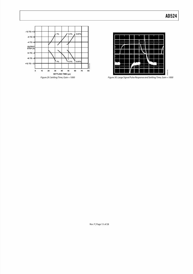
0
Figure 29. Settling Time, Gain = 1000
5mV 10V 20µs
0 0 5 0 0 - 0 3 0
Figure 30. Large Signal Pulse Response and Settling Time, Gain = 1000

8/10/2019 AD524
http://slidepdf.com/reader/full/ad524 14/28
AD524
Rev. F | Page 14 of 28
TEST CIRCUITS
AD524
G = 10
G = 100
G = 1000
10kΩ0.01%
1kΩ10T
10kΩ0.1%
VOUT+VS
–
+
INPUT20V p-p
11kΩ0.1%
1kΩ0.1%
100Ω0.1%
–VS
RG1
RG2
100kΩ0.1%
1
16
13
12 9
11
10
6
3
8
72
0 0 5 0 0 - 0 3 1
Figure 31. Settling Time Test Circuit
–IN
C4C3
+IN
REFERENCE
SENSE
A3
4.44kΩ
404Ω
40Ω
G = 100
G = 1000
Q2, Q4Q1, Q3
+VS
I150µA
I250µA
A1 A2R52
20kΩ
R5520kΩ
VO
CH1
I450µA
–VS
I350µA
VB
R5320kΩ
R5420kΩ
CH2, CH3,CH4
RG2RG1
CH1
CH2,CH3, CH4
R5720kΩ
R5620kΩ
+ +
0 0 5 0 0 - 0 3 2
Figure 32. Simplified Circuit of Amplifier; Gain Is Defined as((R56 + R57)/(RG )) +1; For a Gain of 1, RG Is an Open Circuit

8/10/2019 AD524
http://slidepdf.com/reader/full/ad524 15/28

8/10/2019 AD524
http://slidepdf.com/reader/full/ad524 16/28

8/10/2019 AD524
http://slidepdf.com/reader/full/ad524 17/28
AD524
Rev. F | Page 17 of 28
The AD524 can also be configured to provide gain in the outputstage. Figure 37 shows an H pad attenuator connectedto the reference and sense lines of the AD524. R1, R2, and R3should be made as low as possible to minimize the gain variationand reduction of CMRR. Varying R2 precisely sets the gainwithout affecting CMRR. CMRR is determined by the matchof R1 and R3.
G = 100
G = 1000
G =
G = 10
AD524
+INPUT
–INPUT
+VS
–VS(R1 + R2 + R3)||RL ≥ 2kΩ
VOUT
RL
R12.26kΩ
R25kΩ
R32.26kΩ
(R2||40kΩ) + R1 + R3
(R2||40kΩ)
RG1
RG2
1
16
13
12
11
3
2
8
7
10
69
0 0 5 0 0 - 0 3 7
Figure 37. Gain of 2000
Table 4. Output Gain Resistor Values
Output Gain R2 R1, R3 Nominal Gain2 5 kΩ 2.26 kΩ 2.02
5 1.05 kΩ 2.05 kΩ 5.01
10 1 kΩ 4.42 kΩ 10.1
INPUT BIAS CURRENTS
Input bias currents are those currents necessary to bias theinput transistors of a dc amplifier. Bias currents are anadditional source of input error and must be considered ina total error budget. The bias currents, when multiplied bythe source resistance, appear as an offset voltage. What is ofconcern in calculating bias current errors is the change in biascurrent with respect to signal voltage and temperature. Input
offset current is the difference between the two input biascurrents. The effect of offset current is an input offset voltagewhose magnitude is the offset current times the sourceimpedance imbalance.
AD524
LOAD
+
–
TO POWERSUPPLYGROUND
+VS
–VS
2
3
11
12
13
16
1
8
7
10
6
9
0 0 5 0 0 - 0 3 8
Figure 38. Indirect Ground Returns for Bias Currents—Transformer Coupled
AD524
LOAD
+
–
+VS
–VSTO POWERSUPPLYGROUND
28
7
10
6
9
3
11
12
13
16
1
0 0 5 0 0 - 0 3 9
Figure 39. Indirect Ground Returns for Bias Currents—Thermocouple
AD524
LOAD
+VS
–VS TO POWERSUPPLYGROUND
28
7
10
6
9
3
11
12
13
16
1
+
–
0 0 5 0 0 - 0 4 0
Figure 40. Indirect Ground Returns for Bias Currents–AC-Coupled
Although instrumentation amplifiers have differential inputs,there must be a return path for the bias currents. If this is notprovided, those currents charge stray capacitances, causing theoutput to drift uncontrollably or to saturate. Therefore, whenamplifying floating input sources such as transformers andthermocouples, as well as ac-coupled sources, there must stillbe a dc path from each input to ground.
COMMON-MODE REJECTION
Common-mode rejection is a measure of the change in output voltage when both inputs are changed equal amounts. Thesespecifications are usually given for a full-range input voltagechange and a specified source imbalance. Common-moderejection ratio (CMRR) is a ratio expression whereas common-mode rejection (CMR) is the logarithm of that ratio. Forexample, a CMRR of 10,000 corresponds to a CMR of 80 dB.
In an instrumentation amplifier, ac common-mode rejection isonly as good as the differential phase shift. Degradation of accommon-mode rejection is caused by unequal drops acrossdiffering track resistances and a differential phase shift dueto varied stray capacitances or cable capacitances. In many
applications, shielded cables are used to minimize noise. Thistechnique can create common-mode rejection errors unless theshield is properly driven. Figure 41 and Figure 42 show activedata guards that are configured to improve ac common-moderejection by bootstrapping the capacitances of the input cabling,thus minimizing differential phase shift.
REFERENCE
AD524100Ω
AD711
G = 100
+INPUT
–INPUT
VOUT
+VS
–VS
+
–
RG2
1
12
3
2
8
10
9
6
7
0
0 5 0 0 - 0 4 1
Figure 41. Shield Driver, G ≥ 100
REFERENCE
AD524
100ΩAD712
+INPUT
–INPUT
100Ω
VOUT
+VS
–VS
RG1
RG2
–VS
–
+
1
16
12
3
2
7
6
9
10
8
0 0 5 0 0 - 0 4 2
Figure 42. Differential Shield Driver
8/10/2019 AD524
http://slidepdf.com/reader/full/ad524 18/28
AD524
Rev. F | Page 18 of 28
GROUNDING
Many data acquisition components have two or more groundpins that are not connected together within the device. Thesegrounds must be tied together at one point, usually at the systempower-supply ground. Ideally, a single solid ground would be
desirable. However, because current flows through the groundwires and etch stripes of the circuit cards, and because thesepaths have resistance and inductance, hundreds of millivolts canbe generated between the system ground point and the dataacquisition components. Separate ground returns should beprovided to minimize the current flow in the path from thesensitive points to the system ground point. In this way, supplycurrents and logic-gate return currents are not summed into thesame return path as analog signals where they would causemeasurement errors.
Because the output voltage is developed with respect to thepotential on the reference terminal, an instrumentationamplifier can solve many grounding problems.
DIGITAL P.S.
+5VC –15V
ANALOG P.S.
AD574A
C+15V
6
AD524 AD583SAMPLE
AND HOLD
DIGCOM
DIGITALDATAOUTPUT
SIGNALGROUND
ANALOGGROUND*OUTPUT
REFERENCE
*IF INDEPENDENT; OTHERWISE, RETURN AMPLIFIER REFERENCE TO MECCA AT ANALOG P.S. COMMON.
1µF1µF 1µF0.1µF
0.1µF
0.1µF
0.1µF
2
1
8
710
9
7 9 11 15 1
0 0 5 0
0 - 0 4 3
Figure 43. Basic Grounding Practice
SENSE TERMINAL
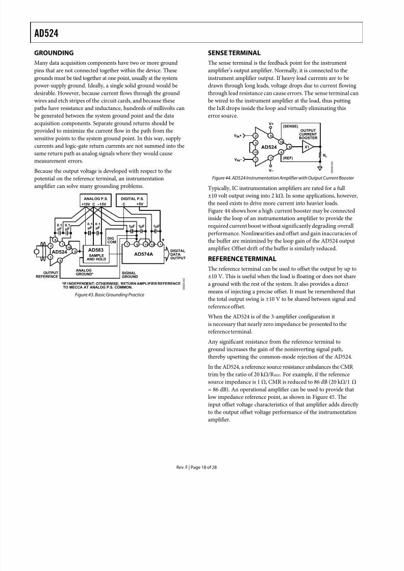
The sense terminal is the feedback point for the instrumentamplifier’s output amplifier. Normally, it is connected to theinstrument amplifier output. If heavy load currents are to bedrawn through long leads, voltage drops due to current flowing
through lead resistance can cause errors. The sense terminal canbe wired to the instrument amplifier at the load, thus puttingthe IxR drops inside the loop and virtually eliminating thiserror source.
V–
V+
X1AD524
(REF)
(SENSE)OUTPUT
CURRENTBOOSTER
RL
VIN+
VIN –
2
3
12
17
6
9
10
8
0 0 5 0 0 - 0 4 4
Figure 44. AD524 Instrumentation Amplifier with Output Current Booster
Typically, IC instrumentation amplifiers are rated for a full±10 volt output swing into 2 kΩ. In some applications, however,the need exists to drive more current into heavier loads.Figure 44 shows how a high current booster may be connectedinside the loop of an instrumentation amplifier to provide therequired current boost without significantly degrading overallperformance. Nonlinearities and offset and gain inaccuracies ofthe buffer are minimized by the loop gain of the AD524 outputamplifier. Offset drift of the buffer is similarly reduced.
REFERENCE TERMINAL
The reference terminal can be used to offset the output by up to±10 V. This is useful when the load is floating or does not share
a ground with the rest of the system. It also provides a directmeans of injecting a precise offset. It must be remembered thatthe total output swing is ±10 V to be shared between signal andreference offset.
When the AD524 is of the 3-amplifier configuration itis necessary that nearly zero impedance be presented to thereference terminal.
Any significant resistance from the reference terminal toground increases the gain of the noninverting signal path,thereby upsetting the common-mode rejection of the AD524.
In the AD524, a reference source resistance unbalances the CMRtrim by the ratio of 20 kΩ/R REF. For example, if the reference
source impedance is 1 Ω, CMR is reduced to 86 dB (20 kΩ/1 Ω= 86 dB). An operational amplifier can be used to provide thatlow impedance reference point, as shown in Figure 45. Theinput offset voltage characteristics of that amplifier adds directlyto the output offset voltage performance of the instrumentationamplifier.

8/10/2019 AD524
http://slidepdf.com/reader/full/ad524 19/28
AD524
Rev. F | Page 19 of 28
AD524
REF
SENSE
LOAD
AD711
+INPUT
–INPUT
R1
R1=== (1 +
R1 )40,000
A2
+
–
VX
IL
RG
ILVX VIN
2
3
13
1
10
9
6
0 0 5 0 0 - 0 4 6
AD524
REF
SENSE
LOAD
AD711 VOFFSET
–VS
+VS
VIN+
VIN –
2 8
10
9
6
7
3
12
1
0 0 5 0 0 - 0 4 5
Figure 45. Use of Reference Terminal to Provide Output OffsetFigure 46. Voltage-to-Current Converter
An instrumentation amplifier can be turned into a voltage-to-current converter by taking advantage of the sense andreference terminals, as shown in Figure 46.
By establishing a reference at the low side of a current settingresistor, an output current may be defined as a function of input
voltage, gain, and the value of that resistor. Because only a smallcurrent is demanded at the input of the buffer amplifier (A2)the forced current, IL, largely flows through the load. Offset anddrift specifications of A2 must be added to the output offset anddrift specifications of the AD524.
Y0
Y2
Y1
+5V
C1 C2
A
B
+5V
–IN
+IN
OUTK1 K2 K3D1 D2 D3
NC
GAIN TABLE
A B GAIN
0011
0101
1010001001
NC = NO CONNECT
1
2
3
4
5
6
7
8
20kΩ
20kΩ
20kΩ 404Ω
4.44kΩ
20kΩ
20kΩ20kΩ
40Ω
PROTECTION
PROTECTION
16
15
14
13
12
11
10
9
INPUTOFFSET
TRIM
ANALOGCOMMON
–VS
+VS
K1 – K3 =THERMOSEN DM2C4.5V COILD1 – D3 = IN4148
INPUTSGAIN
RANGE
A1AD524
LOGICCOMMON
10µF
7407NBUFFERDRIVER
74LS138DECODER
G = 1000K3
G = 100K2
G = 10K1
OUTPUTOFFSETTRIM
RELAYSHIELDS
R110kΩ
+VSR2
10kΩ
1µF35V
1 16
15
14
13
2
3
4
5
6
7
1 16
2
3
4
5
6
7
0 0 5 0 0 - 0 4 7
Figure 47. Three-Decade Gain Programmable Amplifier

8/10/2019 AD524
http://slidepdf.com/reader/full/ad524 20/28
AD524
Rev. F | Page 20 of 28
PROGRAMMABLE GAIN
Figure 47 shows the AD524 being used as a software program-mable gain amplifier. Gain switching can be accomplished withmechanical switches such as DIP switches or reed relays. It shouldbe noted that the on resistance of the switch in series with the
internal gain resistor becomes part of the gain equation and hasan effect on gain accuracy.
The AD524 can also be connected for gain in the output stage.Figure 48 shows an AD711 used as an active attenuator in theoutput amplifier’s feedback loop. The active attenuation presents
very low impedance to the feedback resistors, thereforeminimizing the common-mode rejection ratio degradation.
TO –V
AD524
1
2
3
4
5
6
7
8
16
15
14
13
12
11
10
9
20kΩ
20kΩ
20kΩ 404Ω
4.44kΩ
20kΩ
20kΩ20kΩ
40Ω
PROTECTION
PROTECTION
–IN
+IN
(+INPUT)
(–INPUT)
10kΩ
10pF
20kΩ
AD711
AD7590
GND
39.2kΩ
28.7kΩ
316kΩ
1kΩ
1kΩ
1kΩ
A4A3A2 WR
–VS
VS
1µF35V
INPUTOFFSET
NULL
+VS
OUTPUTOFFSETNULL
R210kΩ
VOUT
+VS
–VS
VDD
VSS VDD
15
13
11
9
2
14
12
10
3 4 5 6 7
1 8 16
0 0 5 0 0 - 0 4 8
+
–
+ –
Figure 48. Programmable Output Gain
2
1
10
6
AD524
DAC A
DB0
256:1
20kΩ
G = 10
G = 100
G = 1000
4.44kΩ
404Ω
40Ω
PROTECTION
20kΩ
20kΩ 20kΩ
20kΩ 20kΩ
DAC B
DB7
AD7528
916
11
12
PROTECTION
3
13
RG1
RG2
Vb
+INPUT(–INPUT)
–INPUT(+INPUT)
VOUT
CS
WR
1/2AD712
1/2AD712
DATAINPUTS
DAC A/DAC B
+VS
4
14
7
15
16
6
18
5
17 3
2
1
19
20
0 0 5 0 0 - 0
4 9
Figure 49. Programmable Output Gain Using a DAC
Another method for developing the switching scheme is touse a DAC. The AD7528 dual DAC, which acts essentially asa pair of switched resistive attenuators having high analog
linearity and symmetrical bipolar transmission, is ideal in thisapplication. The multiplying DAC’s advantage is that it canhandle inputs of either polarity or zero without affecting theprogrammed gain. The circuit shown uses an AD7528 to setthe gain (DAC A) and to perform a fine adjustment (DAC B).
AUTOZERO CIRCUITS
In many applications, it is necessary to provide very accuratedata in high gain configurations. At room temperature, theoffset effects can be nulled by the use of offset trim potenti-ometers. Over the operating temperature range, however,offset nulling becomes a problem. The circuit of Figure 50 shows a CMOS DAC operating in bipolar mode and connectedto the reference terminal to provide software controllable offsetadjustments.

8/10/2019 AD524
http://slidepdf.com/reader/full/ad524 21/28
AD524
Rev. F | Page 21 of 28
WR
CS
+INPUT
G = 10
–INPUT
G = 100
G = 1000
AD7524OUT2
39kΩ
AD589
MSB
LSB
C1
GND
OUT1
AD524
+VS
RG1
RG2
+
–
–
+
–
+
–VSVREF
+VS
+VS
R520kΩ
R320kΩ
R410kΩ
–VS
R65kΩ
1/2AD712
1/2AD712
DATAINPUTS
–VS
28
7
10
6
9
16
13
12
11
3
1
7
6
5 4
1
82
3
3
13
12
11
4
15 14 16
1
2
0 0 5 0 0 - 0 5 0
AD524CG = 100
10kΩ
+10V
350Ω350Ω
350Ω350Ω
14-BITADC
0V TO 2VF.S.
+VS
–VS
RG1
RG2
+
–
2
8
4
5
10
9
6
7
16
13
12
11
3
1
0 0 5 0 0 - 0 5 2
Figure 52. Typical Bridge Application
ERROR BUDGET ANALYSIS
To illustrate how instrumentation amplifier specifications areapplied, review a typical case where an AD524 is required toamplify the output of an unbalanced transducer. Figure 52 shows a differential transducer, unbalanced by 100 Ω, supplyinga 0 mV to 20 mV signal to an AD524C. The output of the IA feeds a 14-bit ADC with a 0 V to 2 V input voltage range. The
operating temperature range is −25°C to +85°C. Therefore, thelargest change in temperature, ∆T, within the operating range isfrom ambient to +85°C (85°C − 25°C = 60°C).
Figure 50. Software Controllable Offset
In many applications, complex software algorithms for autozeroapplications are not available. For those applications, Figure 51 provides a hardware solution.
AD52414
15 16
13
GND
CH
1kΩ
ZERO PULSE
AD7510KD
AD711
A1 A2 A3 A4
VDD
VSS
200µs
9 10
1112 –VS
VOUT
0.1µF LOWLEAKAGE
+VS
RG1
RG2
2
8
7
10
6
9
16
13
12
11
3
1
8
1
2
–
+
–
+
0 0 5 0 0 - 0 5 1
In many applications, differential linearity and resolution are ofprime importance in cases where the absolute value of a variable isless important than changes in value. In these applications, onlythe irreducible errors (45 ppm = 0.004%) are significant. Further-more, if a system has an intelligent processor monitoring theanalog-to-digital output, the addition of an autogain/autozerocycle removes all reducible errors and may eliminate the require-ment for initial calibration. This also reduces errors to 0.004%.
Figure 51. Autozero Circuit

8/10/2019 AD524
http://slidepdf.com/reader/full/ad524 22/28
AD524
Rev. F | Page 22 of 28
Table 5. Error Budget Analysis
Error SourceAD524CSpecifications Calculation
Effect onAbsoluteAccuracyat TA = 25°C
Effect onAbsoluteAccuracyat TA = 85°C
EffectonResolution
Gain Error ±0.25% ±0.25% = 2500 ppm 2500 ppm 2500 ppm –
Gain Instability 25 ppm (25 ppm/°C)(60°C) = 1500 ppm – 1500 ppm –Gain Nonlinearity ±0.003% ±0.003% = 30 ppm – – 30 ppm
Input Offset Voltage ±50 µV, RTI ±50 µV/20 mV = ±2500 ppm 2500 ppm 2500 ppm –
Input Offset Voltage Drift ±0.5 µV/°C–
(±0.5 µV/°C)(60°C) = 30 µV30 µV/20 mV = 1500 ppm
– 1500 ppm –
Output Offset Voltage1 ±2.0 mV ±2.0 mV/20 mV = 1000 ppm 1000 ppm 1000 ppm –
Output Offset Voltage Drif t1 ±25 µV/°C (±25 µV/°C)(60°C)= 1500 µV
1500 µV/20 mV = 750 ppm– 750 ppm –
Bias Current-SourceImbalance Error
±15 nA (±15 nA)(100 Ω ) = 1.5 µV1.5 µV/20 mV = 75 ppm
75 ppm 75 ppm –
Bias Current-SourceImbalance Drift
±100 pA/°C (±100 pA/°C)(100 Ω )(60°C) = 0.6 µV0.6 µV/20 mV = 30 ppm
– 30 ppm –
Offset Current-SourceImbalance Error
±10 nA (±10 nA)(100 Ω ) = 1 µV1 µV/20 mV = 50 ppm
50 ppm 50 ppm –
Offset Current-SourceImbalance Drift
±100 pA/°C (100 pA/°C)(100 Ω )(60°C) = 0.6 µV0.6 µV/20 mV = 30 ppm
– 30 ppm –
Offset Current-SourceResistance-Error
±10 nA (10 nA)(175 Ω ) = 3.5 µV3.5 µV/20 mV = 87.5 ppm
87.5 ppm 87.5 ppm –
Offset Current-SourceResistance-Drift
±100 pA/°C (100 pA/°C)(175 Ω )(60°C) = 1 µV1 µV/20 mV = 50 ppm
– 50 ppm –
Common Mode Rejection 5 V DC 115 dB 115 dB = 1.8 ppm × 5 V = 8.8 µV8.8 µV/20 mV = 444 ppm
444 ppm 444 ppm –
Noise, RTI (0.1 Hz to 10 Hz) 0.3 µV p-p 0.3 µV p-p/20 mV = 15 ppm – – 15 ppm
Total Error 6656.5 ppm 10516.5 ppm 45 ppm
1 Output offset voltage and output offset voltage drift are given as RTI figures.

8/10/2019 AD524
http://slidepdf.com/reader/full/ad524 23/28
AD524
Rev. F | Page 23 of 28
Figure 53 shows a simple application in which the variationof the cold-junction voltage of a Type J thermocouple-iron ±constantan is compensated for by a voltage developed in seriesby the temperature-sensitive output current of an AD590semiconductor temperature sensor.
AD524
IRON
CONSTANTAN
AD590
CU 52.3Ω
8.66kΩ
1kΩ
EO
2.5VAD580
7.5V
G = 100
– 2.5V
1 +52.3Ω
R
TYPE
J
K
E
T
S, R
RA
NOMINALVALUE
REFERENCEJUNCTION+15°C < TA < +35°C
52.3Ω
41.2Ω
61.4Ω
40.2Ω
5.76Ω
+VS
IATA
VA +VS
+
–
–VS
OUTPUTAMPLIFIEROR METER
RT
NOMINAL VALUE9135Ω
RA
EO = VT – VA +52.3ΩIA + 2.5V
MEASURINGJUNCTION
= VT~
VT
0 0 5 0 0 - 0 5 3
Figure 53. Cold-Junction Compensation
The circuit is calibrated by adjusting R T for proper output voltage with the measuring junction at a known referencetemperature and the circuit near 25°C. If resistors with lowtemperature coefficients are used, compensation accuracy isto within ±0.5°C, for temperatures between +15°C and +35°C.
Other thermocouple types may be accommodated with thestandard resistance values shown in Table 5. For other rangesof ambient temperature, the equation in Figure 53 may besolved for the optimum values of R T and R A.
The microprocessor controlled data acquisition system shown
in Figure 54 includes both autozero and autogain capability. Bydedicating two of the differential inputs, one to ground and oneto the A/D reference, the proper program calibration cycles caneliminate both initial accuracy errors and accuracy errors overtemperature. The autozero cycle, in this application, converts anumber that appears to be ground and then writes that samenumber (8-bit) to the AD7524, which eliminates the zero error.Because its output has an inverted scale, the autogain cycleconverts the A/D reference and compares it with full scale. Amultiplicative correction factor is then computed and appliedto subsequent readings.
For a comprehensive study of instrumentation amplifierdesign and applications, refer to the Designer’s Guide to Instrumentation Amplifiers (3rd Edition), available free fromAnalog Devices, Inc.
AD524
AD7524
AD574A
AD583
AGND
20kΩ
10kΩ
5kΩ
AD7507
CONTROL
DECODELATCH
ADDRESS BUS
A0, A2,
EN, A1
VIN
VREF
MICRO-PROCESSOR
+
–
RG2
RG1
–VREF
20kΩ
1/2AD7121/2
AD712
–
+ –
+
2
10
6
9
16
13
12
11
3
1
0 0 5 0 0 - 0 5 4
Figure 54. Microprocessor Controlled Data Acquisition System

8/10/2019 AD524
http://slidepdf.com/reader/full/ad524 24/28
AD524
Rev. F | Page 24 of 28
OUTLINE DIMENSIONS
16
1 8
90.310 (7.87)
0.220 (5.59)PIN 1
0.080 (2.03) MAX0.005 (0.13) MIN
SEATINGPLANE
0.023 (0.58)
0.014 (0.36)
0.060 (1.52)
0.015 (0.38)0.200 (5.08)
MAX
0.200 (5.08)
0.125 (3.18)0.070 (1.78)
0.030 (0.76)
0.100(2.54)BSC
0.150(3.81)MIN
0.840 (21.34) MAX
0.320 (8.13)0.290 (7.37)
0.015 (0.38)
0.008 (0.20)
CONTROLLING DIMENSIONS ARE IN INCHES; MILLIMETER DIMENSIONS(IN PARENTHESES) ARE ROUNDED-OFF INCH EQUIVALENTS FORREFERENCE ONLY AND ARE NOT APPROPRIATE FOR USE IN DESIGN.
Figure 55. 16-Lead Side-Brazed Ceramic Dual In-Line [SBDIP](D-16)
Dimensions shown in inches and (millimeters)
CONTROLLING DIMENSIONS ARE IN INCHES; MILLIMETER DIMENSIONS(IN PARENTHESES) ARE ROUNDED-OFF INCH EQUIVALENTS FORREFERENCE ONLY AND ARE NOTAPPROPRIATE FOR USE IN DESIGN.
1
20 4
9
8
13
19
14
3
18
BOTTOMVIEW
0.028 (0.71)
0.022 (0.56)
45° TYP
0.015 (0.38)MIN
0.055 (1.40)
0.045 (1.14)
0.050 (1.27)BSC
0.075 (1.91)REF
0.011 (0.28)
0.007 (0.18)R TYP
0.095 (2.41)
0.075 (1.90)
0.100 (2.54) REF
0.200 (5.08)REF
0.150 (3.81)BSC
0.075 (1.91)REF
0.358 (9.09)
0.342 (8.69)
SQ
0.358(9.09)MAX
SQ
0.100 (2.54)
0.064 (1.63)
0.088 (2.24)
0.054 (1.37)
0 2 2 1 0 6 - A
Figure 56. 20-Terminal Ceramic Leadless Chip Carrier [LCC]
(E-20)Dimensions shown in inches and (millimeters)
CONTROLLING DIMENSIONSARE IN MILLIMETERS; INCH DIMENSIONS(IN PARENTHESES) ARE ROUNDED-OFF MILLIMETER EQUIVALENTS FOR
REFERENCE ONLYAND ARE NOT APPROPRIATE FOR USE IN DESIGN.
COMPLIANT TO JEDEC STANDARDS MS-013-AA
0 3 2 7 0 7 - B
10.50 (0.4134)
10.10 (0.3976)
0.30 (0.0118)
0.10 (0.0039)
2.65 (0.1043)
2.35 (0.0925)
10.65 (0.4193)
10.00 (0.3937)
7.60 (0.2992)
7.40 (0.2913)
0.75 (0.0295)
0.25 (0.0098) 45°
1.27 (0.0500)
0.40 (0.0157)
COPLANARITY0.10 0.33 (0.0130)
0.20 (0.0079)
0.51 (0.0201)
0.31 (0.0122)
SEATINGPLANE
8°0°
16 9
81
1.27 (0.0500)BSC
Figure 57. 16-Lead Standard Small Outline P ackage [SOIC_W]Wide Body (RW-16)
Dimensions shown in millimeters and (inches)

8/10/2019 AD524
http://slidepdf.com/reader/full/ad524 25/28

8/10/2019 AD524
http://slidepdf.com/reader/full/ad524 26/28
AD524
Rev. F | Page 26 of 28
NOTES

8/10/2019 AD524
http://slidepdf.com/reader/full/ad524 27/28

8/10/2019 AD524
http://slidepdf.com/reader/full/ad524 28/28
AD524
NOTES
©2007 Analog Devices, Inc. All rights reserved. Trademarks andregistered trademarks are the property of their respective owners.