Embed Size (px)
Citation preview
Abstract— The topology for simulating the floating inductance
simulator circuit based on employing voltage differencing
buffered amplifiers (VDBAs) as new active components has been
described in this work. The realized floating inductance simulator
circuit uses two VDBAs and only one grounded capacitor. The
circuit is resistorless and canonical structure as well as attractive
for integration. The resulting equivalent inductance value of the
proposed simulator can be adjusted electronically through the
transconductance parameter of the VDBA. As illustrative
application example, the proposed tunable floating inductance
simulator is employed to realize the second-order RLC bandpass
filter. Simulation results using standard 0.35 µm BiCMOS process
model are included to verify the theoretical analysis.
Index Terms— voltage differencing buffered amplifier (VDBA),
voltage-mode circuit, floating inductance simulator, BiCMOS
technology
I. INTRODUCTION
loating inductance simulation circuit is one of the most important circuit elements widely used in many applications such as oscillator design, filter design and
cancellation of parasitic elements. However, unfortunately, a large-valued physical inductor is not allowed to fabricate in the integrated circuit technology because of a large chip area and high-cost requirements. Although on chip spiral inductors with low quality factor (Q) can be performed to alleviate this restriction, their values are very small, usually in order of 1 nH. Accordingly, to overcome this problem, many actively simulated floating inductor circuits using various high-performance active devices have been reported in literature [1]-[10]. However, all of them need a large number of active and passive elements for their realizations.
Manuscript received December 22, 2015; revised January 19, 2016.
This work was supported in part by Faculty of Engineering, Department of
Electronic and Telecommunication Engineering, Rajamangala University of
Technology Isan (RMUTI), Khonkaen Campus.
O. Channumsin is with the Faculty of Engineering, Rajamangala
University of Technology Isan (RMUTI), Khonkaen Campus., Srichan road,
Muang, KhonKaen, 40000, Thailand (e-mail: [email protected]).
W. Tangsrirat is with the Faculty of Engineering, King Mongkut’s Institute
of Technology Ladkrabang (KMITL), Chalongkrung road, Ladkrabang,
Bangkok 10520, Thailand (phone: +662-326-4205; fax: +662-326-4205;
e-mail: [email protected]).
Lately, the new active building block called voltage differencing buffered amplifier (VDBA) is introduced in [11], to provide the alternative possibility of electronically controllable voltage-mode analog signal processing circuits and solutions. Several applications based on using VDBAs as active elements in mainly analog signal processing have been developed [12]-[18]. This work presents an actively floating inductance simulator topology using two VDBAs and one grounded capacitor. The proposed synthetic floating inductor is electronically tunable through the transconductance gain of the VDBA. The performance of the proposed floating simulator circuit is provided for illustrative example of the active RLC bandpass filter design. PSPICE simulation results with standard 0.35-µm BiCMOS process parameters are obtained to confirm the theory.
vp vw
iz
vz
ip
w
z
p
VDBA
vn
in
n
iw
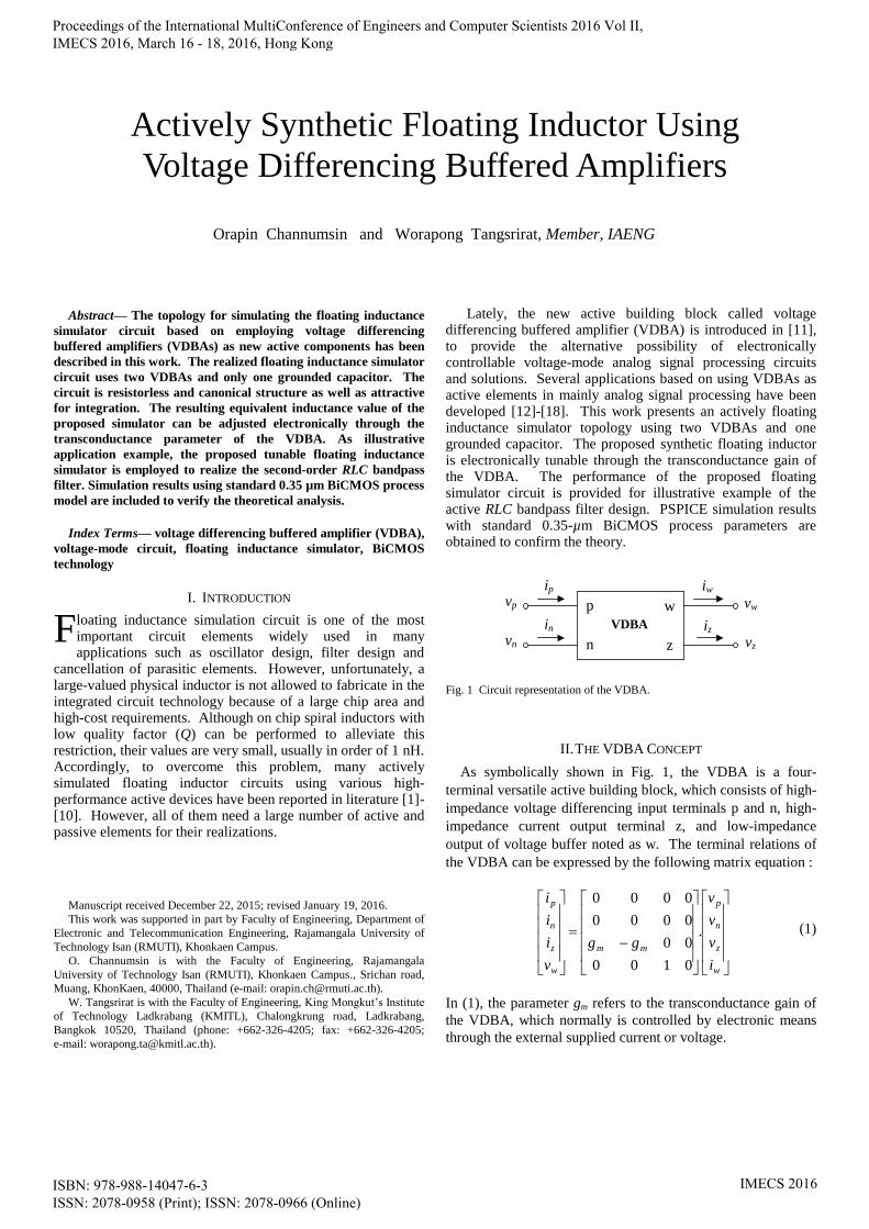
Fig. 1 Circuit representation of the VDBA.
II. THE VDBA CONCEPT
As symbolically shown in Fig. 1, the VDBA is a four-
terminal versatile active building block, which consists of high-
impedance voltage differencing input terminals p and n, high-
impedance current output terminal z, and low-impedance
output of voltage buffer noted as w. The terminal relations of
the VDBA can be expressed by the following matrix equation :
w
z
n
p
mm
w
z
n
p
i
v
v
v
gg
v
i
i
i
.
0100
00
0000
0000
(1)
In (1), the parameter gm refers to the transconductance gain of
the VDBA, which normally is controlled by electronic means
through the external supplied current or voltage.
Orapin Channumsin and Worapong Tangsrirat, Member, IAENG
Actively Synthetic Floating Inductor Using
Voltage Differencing Buffered Amplifiers
F
Proceedings of the International MultiConference of Engineers and Computer Scientists 2016 Vol II, IMECS 2016, March 16 - 18, 2016, Hong Kong
ISBN: 978-988-14047-6-3 ISSN: 2078-0958 (Print); ISSN: 2078-0966 (Online)
IMECS 2016
Q5
M3
M5
+V
iz
z
Q6
-V
M2M1
pn
IB
IA IA
IB
Q3 Q4Q1 Q2M4
w
M6
M7
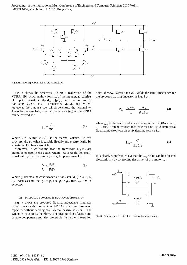
Fig.2 BiCMOS implementation of the VDBA [19].
Fig. 2 shows the schematic BiCMOS realization of the
VDBA [19], which mainly consists of the input stage consists
of input transistors M1-M2, Q1-Q4, and current mirror
transistors Q5-Q6, M3. Transistors M4-M5 and M6-M7
represents the output stage, which constitute the terminal w.
The effective small-signal transconductance (gm) of the VDBA
can be derived as :
T
Bm
V
Ig
2 (2)
Where VT 26 mV at 27C is the thermal voltage. In this
structure, the gm-value is tunable linearly and electronically by
an external DC bias current IB.
Moreover, if we assume that the transistors M4-M7 are
biased to operate in the active region. As a result, the small-
signal voltage gain between vw and vz is approximated to :
75
64
gg
gg
v
v
z
w (3)
Where gi denotes the conductance of transistor Mi (i = 4, 5, 6,
7). Also assume that g4 g5 and g6 g7, thus vw vz as
expected.
III. PROPOSED FLOATING INDUCTANCE SIMULATOR
Fig. 3 shows the proposed floating inductance simulator
circuit constructing only two VDBAs and one grounded
capacitor without needing any external passive resistors. The
synthetic inductor is, therefore, canonical number of active and
passive components and also preferable for further integration
point of view. Circuit analysis yields the input impedance for
the proposed floating inductor in Fig. 2 as :
21
121
mmL
ingg
sC
i
vvZ
(4)
where gmi is the transconductance value of i-th VDBA (i = 1,
2). Thus, it can be realized that the circuit of Fig. 3 simulates a
floating inductor with an equivalent inductance Leq:
21
1
mm
eqgg
CL (5)
It is clearly seen from eq.(5) that the Leq–value can be adjusted
electronically by controlling the values of gm1 and/or gm2.
p
w
VDBA
iL
n
z
1
v1
n
p
VDBA
z
w
2iL
v2
C1
Fig. 3. Proposed actively simulated floating inductor circuit.
Proceedings of the International MultiConference of Engineers and Computer Scientists 2016 Vol II, IMECS 2016, March 16 - 18, 2016, Hong Kong
ISBN: 978-988-14047-6-3 ISSN: 2078-0958 (Print); ISSN: 2078-0966 (Online)
IMECS 2016
IV. PERFROMANCE SIMULATIONS
To verify the theoretical prediction, the proposed circuit
in Fig. 3 was simulated with PSPICE program. To
implement the VDBA device in the following simulation
purpose, the BiCMOS technology structure depicted in
Fig. 2 has been employed using 0.35-µm BiCMOS
technology [19]. Transistor aspect ratios (W/L in µm/µm)
were set as : 14/0.7 and 28/0.7 for all NMOS and PMOS
transistors respectively. The DC supply voltages and bias
currents were respectively chosen as : +V= -V= 1 V and
IA = 25 µA.
1.00 1.01 1.02 1.03 1.04 1.05 1.06 1.07 1.08 1.09 1.10-150
-100
-50
0
50
100
150
-40
-20
0
20
40
Current
(uA)
Voltage
(mV)
Time(ms)
vin
iL
Fig. 4. Time-domain responses for vin and iL of the floating inductor of
Fig. 3.
1k 10k 100k 1M 10M1
100
10k
1M
100M
Man
gn
itu
de
(W)
Frequency (Hz)
Simulated
Theory
gm = 0.98 mA/V
gm = 1.92 mA/V
gm = 2.88 mA/V
(a)
1k 10k 100k 1M 10M0
100
200
300
Frequency (Hz)
Ph
ase
(deg
ree)
Theory
gm =2.88 mA/V
gm = 1.92 mA/V
gm = 0.98 mA/V
(b)
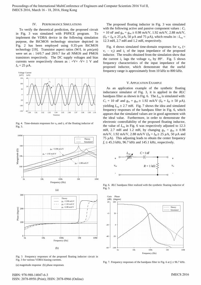
Fig. 5 Frequency responses of the proposed floating inductor circuit in
Fig. 3 for various VDBA biasing currents.
(a) magnitude response (b) phase responses
The proposed floating inductor in Fig. 3 was simulated
with the following active and passive component values : C1
= 10 nF and gm = gmi 0.98 mA/V, 1.92 mA/V, 2.88 mA/V,
(IB = IBi 25 µA, 50 µA and 75 µA), which results in : Leq =
12.3 mH, 2.7 mH and 1.2 mH, respectively.
Fig. 4 shows simulated time-domain responses for vin (=
v1 – v2) and iL of the input impedance of the proposed
inductor. The results obtained from the simulation show that
the current iL lags the voltage vin by 89. Fig. 5 shows
frequency characteristics of the input impedance of the
proposed inductor, which demonstrate that the useful
frequency range is approximately from 10 kHz to 800 kHz.
V. APPLICATION EXAMPLE
As an application example of the synthetic floating
inductance simulator of Fig. 3, it is applied in the RLC
bandpass filter as shown in Fig. 6. The Leq is simulated with:
C1 = 10 nF and gm = gmi 1.92 mA/V (IB = IBi 50 µA), yielding Leq 2.7 mH. Fig. 7 shows the idea and simulated
frequency responses of the bandpass filter in Fig. 6, which
appears that the simulated values are in good agreement with
the ideal value. Furthermore, in order to demonstrate the
electronic controllability of the proposed floating inductor,
the value of Leq in Fig. 6 was respectively adjusted to 12.3
mH, 2.7 mH and 1.2 mH, by changing gm = gmi 0.98
mA/V, 1.92 mA/V, 2.88 mA/V (IB = IBi 25 µA, 50 µA and
75 µA). This adjusting leads to obtain the center frequency
fc 45.3 kHz, 96.7 kHz and 145.1 kHz, respectively.
Leq
vo
+
-
R = 1 kW
C = 1 nF
vin
+
-
Fig. 6. RLC bandpass filter realized with the synthetic floating inductor of
Fig. 3.
1k 10k 100k 1M 10M-60
-40
-20
-0
20
-100
-50
0
50
100
Simulated
Theory
Frequency (Hz)
Phase
(degree)
Gain
(dB)
Fig. 7. Frequency responses of the bandpass filter in Fig. 6 at fc 96.7 kHz.
Proceedings of the International MultiConference of Engineers and Computer Scientists 2016 Vol II, IMECS 2016, March 16 - 18, 2016, Hong Kong
ISBN: 978-988-14047-6-3 ISSN: 2078-0958 (Print); ISSN: 2078-0966 (Online)
IMECS 2016

Frequency (Hz)
1k 10k 100k 1M 10M-60
-40
-20
-0
20
Vo
ltag
e g
ain
(d
B) Simulated
Theory
Leq = 2.7 mH (fc = 96.7 kHz)
Leq = 12.3 mH (fc = 45.3 kHz) Leq = 1.2 mH (fc = 145.1 kHz)
Fig. 8. Gain responses of Fig. 6 with electronically variable Leq.
VI. CONCLUSION
The floating inductance simulator has been presented in
this paper. The circuit contains only two VDBAs and one
grounded capacitor, which is desired for further integrated
circuit implementation. The equivalent inductance values
can be adjusted electronically through the gm-value of the
VDBA. The proposed circuit is demonstrated on the RLC
bandpass filter design example. The workability of the
proposed structure has been supported by PSPICE
simulations using standard 0.35-m BiCMOS technology.
REFERENCES
[1] C. Psychalinos and A. Spanidou, “Current amplifier-based grounded and floating inductance simulators”. Int. J. Electron. Commun. (AEU), vol. 60, pp. 168-171, 2006.
[2] E. Yuce, “Inductor implementation using a canonical number of active and passive elements”, Int. J. Electron., vol.94, no.4, pp.317-326, 2007.
[3] E. Yuce, “On the implementation of the floating simulators employing a single active element”, Int. J. Electron. Commun. (AEU), vol.61, no.7, pp.453-458, 2007.
[4] M. Sagbas, U. E. Ayten, H. Sedef and M. Koksal, “Electronically tunable floating inductance simulator”, Int. J. Electron.Commun. (AEU), vol.63, pp.423-4278, 2009.
[5] E. Yuce, S. Minaei, “Novel floating simulated inductors with wider operating-frequency ranges”, Microelectron. J., vol.40, pp.928-938, 2009.
[6] D. Prasad, D. R. Bhaskar, and A. K. Singh, “New grounded and floating simulated inductance circuits using current differencing transconductance amplifiers”, Radioengineering, vol.19, no.1, pp.194-198, 2010.
[7] E. Yuce, “A novel floating simulation topology composed of only grounded passive elements”, Int. J. Electron., vol.97, no.3, pp.249-262, 2010.
[8] J. W. Horng, “Lossless inductance simulation and voltage-mode universal biquadratic filter with one input and five outputs using DVCCs”, Analog Integr. Circuits Signal Process., no.62, pp.407–413, 2010.
[9] M. A. Ibrahim, S. Minaei, E. Yuce, N. Herencsar and J. Koton, “Lossy/lossless floating/grounded inductance simulation using one DDCC”, Radioengineering, vol.21, no.1, pp.3-10, 2012.
[10] U. E. Ayten, M. Sagbas, N. Herencsar and J. Koton, “Novel general element simulators using CBTA”, Radioengineering, vol.21, no.1, pp.11-19, 2012.
[11] D. Biolek, R. Senani, V. Biolkova, Z. Kolka, “Active elements for analog signal processing: classification, review, and new proposals”, Radioengineering, vol. 17 no. 4, pp.15-32, 2008.
[12] V. Biolkova, Z. Kolka, D. Biolek, “Fully balanced voltage differencing buffered amplifier and its applications”, Proc. of The 52nd MWSCAS, Aug.2-5, Cancun, Mexico, pp.45-48, 2009.
[13] A. Yesil, F. Kacar and K. Gurkan, “Lossless grounded inductance simulator employing single VDBA and its experimental band-pass filter application”, Int. J. Electron. Commun. (AEU), vol.68, pp.143-150, 2014.
[14] F. Kacar, A. Yesil, A. Noori, “New CMOS realization of voltage differencing buffered amplifier and its biquad filter application”, Radioengineering, vol. 21, no.1, pp. 333-339, 2012.
[15] N. Khatib and D. Biolek, “New voltage mode universal filter based on promising structure of voltage differencing buffered amplifier”, Proc. of The 23th Radioelektronika, April 16-17, Pardubice, Czech Republic, pp. 171-181, 2013.
[16] R. Sotner, J. Jerabek, N. Herencsar, “Voltage differencing buffered/inverted amplifiers and their applications for signal generation”, Radioengineering, vol.22, no.2, pp.490-504, 2013.
[17] A. Gilney, E. Alaybeyoglu and H. Kuntman, “New CMOS realization of z copy voltage differencing buffered amplifier and its current-mode filter appliction”, Proc. of The 8th DTIS, March 26-28, Abu Dhabi, United Arab Emirates, pp. 68 – 71, 2013.
[18] P. Whig and S. N. Ahmad, “CMOS integrated VDBA-ISFET device for water quality monitoring”, International Journal of Intelligent Engineering and Systems, vol. 7, no.1, 2014.
[19] W. Tangsrirat, O. Onjan, T. Pukkalanun, “ BiCMOS Realization of Voltage Differencing Buffered Amplifier (VDBA) and Its Application”,Proc. of The 29th ITC-CSCC,July 1-4, Phuket, Thailand, 2014.
Proceedings of the International MultiConference of Engineers and Computer Scientists 2016 Vol II, IMECS 2016, March 16 - 18, 2016, Hong Kong
ISBN: 978-988-14047-6-3 ISSN: 2078-0958 (Print); ISSN: 2078-0966 (Online)
IMECS 2016