Embed Size (px)
Citation preview

1
Active Clamp Flyback (Part I) Pei-Hsin Liu

What will I get out of this session?
• Purpose: • Relevant End Equipments:
1. Demo TI’s knowledge base on high- density adapter 2. Fundamental of ACF operation and challenge on ZVS control
1. High Density AC Adapter or Charger 2. USB Power Delivery Chargers 3. AC/DC or DC/DC Auxiliary Power Supply

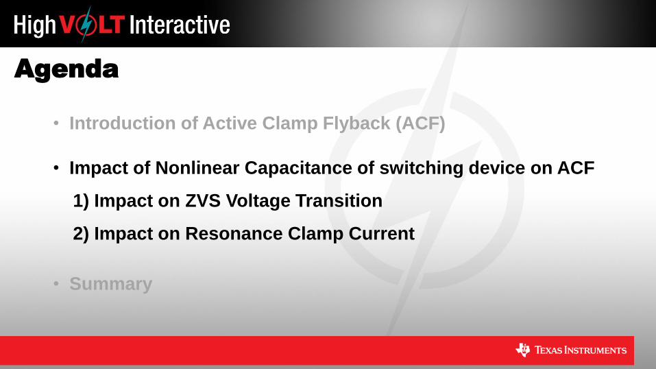
Agenda
• Introduction of Active Clamp Flyback (ACF)
• Impact of Nonlinear Capacitance of switching device on ACF
1) Impact on ZVS Voltage Transition
2) Impact on Resonance Clamp Current
• Summary

65W Adapter
Topology Power
Density fsw
(kHz) Primary Switches
High-side drivers
Switching Devices
A Passive-clamp Flyback (PCF) 11W/in3 150~260 1 pcs 0 pcs Si
B Active-clamp Flyback (ACF) 14W/in3 120~165 2 pcs 1 pcs SiC/Si
C Three-level LLC 17W/in3 300~500 4 pcs 3 pcs Si
Soft
switching
Adapter Density and Eff Comparison
Flyback: PCF or ACF Three-level LLC
Vac
ᵑ ACF (B)
3-Level LLC (A)
ACF (B)
PCF(A)
3-level LLC (C)
(V)
Ca
ble
-en
d E
ff. (%
) 20V/65W output

Issues of DCM Flyback + Passive Clamp
Vbulk NVo
NVo Vclamp
fsw
im(+)
2
( )
1
2
clamp
clamp k m sw
clamp o
VP L i f
V NV
Clamp Loss:
RM6 XFMR (N=3.25, Lk=3uH), 650V/650mΩ Silicon FET
Vclamp=130V, 20V/30W, Vbulk=230 2V
100k 200k 300k 1
2
3
4
5
6
7
Pe
rcen
tage (
%)
fsw (Hz)
PSwitching/30W
PClamp/30W
21
2Switching sw bulk swP C V fSwitching Loss:

C ≈0 (to output) ≈0 (ZVS) Middle Higher
Transition Mode (TM) + Active Clamp
(A) Passive-clamp + DCM (B) Passive-clamp + TM
PClamp PSwitching PCore PWinding
A High Higher Higher Mid
B High Mid Lower Lower
Vbulk
(C) Active-clamp + TM
Due to higher im(-) and iclamp

I VI
V IV
II III
Operation of Active Clamp Flyback (ACF)
I
im
Vgs(QH)
Vsw
iclamp
iQL
isec
Vgs(QL)
Region II : After QL off, im charges Coss(QL) and discharge Coss(QH)
so Vsw rises to Vbulk+Vclamp before QH turns on
Region I : As QL on, im peak increases and Lm stores energy
Region I Region II VII

Operation of ACF: (III to IV)
Region IV : After QH on, N·Vo demagnetizes Lm, so im decades.
Cclamp resonating with Lk stores Lk energy.
Lm releases energy to output, isec = (im-iclamp)N
Region III : im forces QH body diode on, so Vclamp charges to N·Vo
Region III Region IV
I VI
V IV
II III
I
im
Vgs(QH)
Vsw
iclamp
iQL
isec
Vgs(QL)
VII

Region V
Operation of ACF: (V to VI)
Region VI : Output diode switches off as isec resonating to 0A (ZCS).
Vclamp demagnetizes Lm, so im decades more negatively.
Region V : Cclamp resonating with Lk releases Lk energy to output.
Region VI
I VI
V IV
II III
I
im
Vgs(QH)
Vsw
iclamp
iQL
isec
Vgs(QL)
VII

Region I
Operation of ACF: (VII to I)
Region I : QL turns on as Vsw close to 0V (zero voltage switching, ZVS)
Region VII : After QH off, im(-) discharges Coss(QL) and charges Coss(QH)
so Vsw falls from Vbulk+Vclamp to 0V
I VI
V IV
II III
I
im
Vgs(QH)
Vsw
iclamp
iQL
isec
Vgs(QL)
VII Region VII
2 2
( )
1 1
2 2m m sw swL i C V
ZVS criteria:
im(-)

For GaN: Linear scaling between Rds(on) and Coss
Effect on Coss Nonlinearity:
Vds (V)
Co
ss (
pF
)
Junction Capacitance of Si and GaN
ipri
iclamp
+1.8A
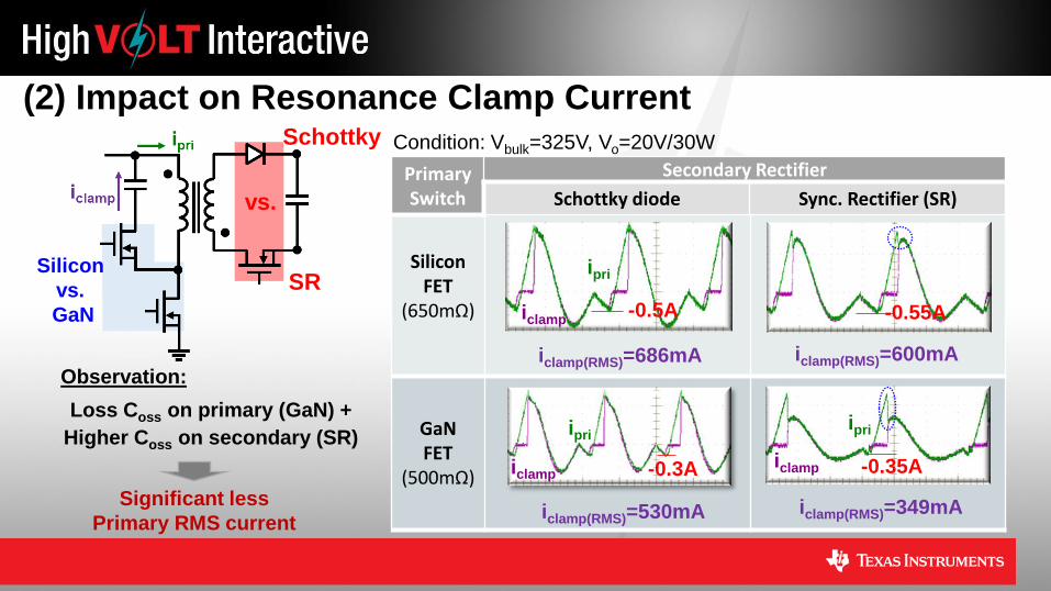
-0.5A
+1.44A
-0.3A
ipri
iclamp
Coss = 47pF (680mΩ Si FET)
Coss = 15pF (500mΩ GaN FET)
iclamp(RMS)=686mA
iclamp(RMS)=530mA
im(pk-pk)=2.25A
im(pk-pk)=1.74A
For Si: lower Rds(on) → more Coss nonlinearity
GaN FET 500mΩ
GaN FET 150mΩ
Si FET 680mΩ
Si FET 180mΩ
2 2
( )
1 1
2 2m m sw dsL i C V ZVS criteria:
ipri(RMS)=810mA
ipri(RMS)=612mA
+1.8A
Agenda
• Introduction of Active Clamp Flyback (ACF)
• Impact of Nonlinear Capacitance of switching device on ACF
1) Impact on ZVS Voltage Transition
2) Impact on Resonance Clamp Current
• Summary

Vds (V) C
oss (
pF
)
GaN FET
(500mΩ)
Si FET
(680mΩ)
1000
100
10
1 1 10 100
(1) Impact on ZVS Voltage Transition
Si FET (680mΩ)
GaN FET (500mΩ)
From QH
From QL
Affect:
(1) Longer dead time → fsw limitation
(QH off to QL on)
(2) Virtual short as gate off→ Higher im(-)
Vsw

Cclamp design to Reduce Upper Flat Area
(Cclamp=100nF) Vgs(QH)
Vsw
iclamp
im
im(-) -0.9A
340ns
Improve: Resonance > QH on time to reduce its nonlinear cap effect
2 2
( )
1 1
2 2m m sw dsL i C V
ZVS
Criteria: 2 2 2
( ) ( )
1 1 1
2 2 2m m k clamp sw dsL i L i C V
ZVS
Criteria:
0.8
0
-0.8
Cu
rre
nt (A
)
0
200
400
Vo
lta
ge
(V
)
(180mΩ Si FET)
(Cclamp=600nF)
Vgs(QH)
Vsw
iclamp
im
340ns
0.8
0
-0.8 Curr
en
t (A
)
0
200
400
Vo
lta
ge
(V
)
iclamp(-)
im(-) -0.8A
(180mΩ Si FET)

Partial ZVS to Reduce Lower Flat Area
ipri
(RMS=0.717A)
Vsw
Full
ZVS
Vds (V)
Co
ss (
pF
)
Si FET
680mΩ
1.5nF
Vsw
Partial
ZVS
ipri
(RMS=0.626A)
26.2% less
conduction loss !!
263pF
Condition: 20V/30W, RM6, C3/C3 (SPP02N60C3), Secondary SR (BSC360N15NS3)
Vbulk (V) DC
/DC
Eff
icie
ncy
Full ZVS
Partial ZVS 0.93
0.92
0.91 70 170 270 370
1000
100
10
1 1 10 100

Trade-off of Partial ZVS for Si FET
Lo
ss
Re
du
cti
on
(W
)
ZVS point (V)
Condition: 20V/30W, RM6, C3/C3 (SPP02N60C3),
Secondary SR (BSC360N15NS3)
Vbulk=375V
Vsw
Vsw
For Si, larger loss reduction at 10V; Peak at 20V
For GaN, full ZVS gives best efficiency
0.14
0.1
0.06
0.02
0 10 20 30 40 50 60
(gain) Conduction
loss reduction
i pri
(RM
S) (A
)
ZVS
point (V)
0.75
0.69
0.63
0.57 0 10 20 30 40 50 60
(Lost) Turn-on
loss increasing PS
wit
ch
ing
(W
)
ZVS
point (V)
0.42
0.28
0.14
0 0 10 20 30 40 50 60
GaN FET
(500mΩ)
Silicon FET
(650mΩ)
Primary Switch
Secondary Rectifier
Schottky diode Sync. Rectifier (SR)
(2) Impact on Resonance Clamp Current
-0.3A
ipri
iclamp
iclamp(RMS)=530mA
Observation:
Loss Coss on primary (GaN) +
Higher Coss on secondary (SR)
Significant less
Primary RMS current
Condition: Vbulk=325V, Vo=20V/30W
-0.5A
ipri
iclamp
iclamp(RMS)=686mA
ipri
-0.35A
iclamp(RMS)=349mA
iclamp
-0.55A
iclamp(RMS)=600mA
Silicon
vs.
GaN
vs.
SR
Schottky
Coss(SR)/N2
(V)
Coss(QH): Si
Co
ss (
pF
)
1000
100
10 1 10 100
ipri
im
(A)
Voltage polarity change on Lk
eliminates the current dip.
1.6
1.2
0.8
Si FET: Slower dVsw/dt, Less dipri/dt
Silicon
Vpri
NVsec (low Coss(QH))
(high Coss(QH))
(high Coss(SR))
10ns/div
Vpri < N·Vsec as
higher Coss(QH)
(V) 60
20
-20
sec
1[ ]
pri
pri
k
diN V V
dt L
ipri
iclamp
1μs/div 1
A/d
iv

GaN FET: Faster dVsw/dt, Larger dipri/dt
sec
1[ ]
pri
pri
k
diN V V
dt L
GaN
Coss(SR)/N2
(V)
Coss(QH): GaN
Co
ss (
pF
)
1000
100
10 1 10 100
Vpri NVsec
(high Coss(SR))
10ns/div
Vpri > N·Vsec
as Vsw rising
(V)
0
-100
-200
-300
ipri
iclamp
1μs/div 1
A/d
iv
ipri
im
(A)
Negative di/dt reduces iclamp, so
more im is delivered to output.
1.3
1.1
0.9
0.7
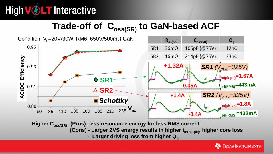
Vac
SR1
Schottky
SR2
0.95
0.93
0.91
0.89 85 110 235 60 135 160 185 210
AC
/DC
Eff
icie
ncy
Trade-off of Coss(SR) to GaN-based ACF
SR1
Schottky
Condition: Vo=20V/30W, RM6, 650V/500mΩ GaN Rds(on) Coss(SR) Qg
SR1 36mΩ 106pF (@75V) 12nC
SR2 16mΩ 214pF (@75V) 23nC
SR2
Higher Coss(SR): (Pros) Less resonance energy for less RMS current
(Cons) - Larger ZVS energy results in higher im(pk-pk), higher core loss
- Larger driving loss from higher Qg
+1.32A
ipri
ipri(RMS)=443mA
im(pk-pk)=1.67A
SR1 (Vbulk=325V)
-0.35A
+1.4A
-0.4A
ipri
SR2 (Vbulk=325V)
ipri(RMS)=432mA
im(pk-pk)=1.8A

Full-Load Eff Comparison: GaN vs. Si
Vbulk (V)
i pri(R
MS
) (A
)
Vbulk (V)
DC
/DC
Effic
ien
cy (
%)
600V Si +
Partial ZVS
650V GaN+
Full ZVS
3% 2%
600V Si+
Partial ZVS
Condition: 20V/30W, RM6, SR (BSC360N15NS3), Si FET(600V, 680mΩ) ; GaN (650V, 500mΩ)
Eff difference at low line will >2% as including input stage !
650V GaN+
Full ZVS
600V Si+
Partial ZVS

Conclusion
• Clamping and switching losses are the limitation of passive clamp flyback converter.
• Active clamp flyback (ACF) eliminates clamping and switching losses in tradeoff with
conduction loss and transformer core loss.
• GaN-based ACF has advantage over silicon due to less winding loss and core loss.
• Coss nonlinearity impact and potential solutions using Si FET are addressed.
(a) Clamp cap design to overcome high Coss on the high-side switch
(b) Partial ZVS to overcome high Coss on the low-side switch


![Catalogue FLYBACK Equivalent - [PDF Document] FLYBACK Equivalent FlyBack Equivalent flyback reemplazo conversor Flyback tv fly-back Flyback Tester Flyback Converter conversor Flyback](https://img.dokumen.tips/doc/110x75/5a832a447f8b9a9d308e9416/catalogue-flyback-equivalent-pdf-document-flyback-equivalent-flyback-equivalent.jpg)