Embed Size (px)
Citation preview
ACT50 DESIGN GUIDE Innovative PowerTM June 2010
Copyright © 2010 Active-Semi, Inc. - - www.active-semi.com
AC/DC LED Lighting
DESIGN GUIDE
Jan 2011

ACT364/50 DESIGN GUIDE Innovative PowerTM June 2010
Copyright © 2010 Active-Semi, Inc. - 2 - www.active-semi.com
Table of Contents
ACT364 1W 350mA(3.5V) .....3
ACT364 3W 700mA(4V) ........5
ACT364 3W 350mA(12V) ......7
ACT365 7.8W 350mA(26V) PAR30.........9
ACT50 5W 350mA(15V) ......11
ACT50 5W 128mA(49V) ......13
ACT50 7W 350mA(28V) ......15
ACT50 12W 350mA(35V) Non-Isolated.......17
ACT50 12W 350mA(35V) PAR38.......19
ACT50 12W 350mA(35V) High Efficiency......21
ACT50 21W 750mA(28V)....23
Copyright © 2010 Active-Semi, Inc. - 3 - www.active-semi.com
ACT364 DESIGN GUIDE Innovative PowerTM Sep 2010
(1.1)
OUTCV
SW
2
CSPOUTCC V
FR
9.0396.0L
21
I
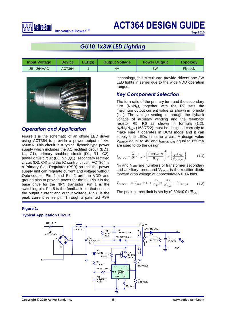
Input Voltage LED(s) Output Voltage Power Output Topology
85 - 264VAC 1 3.5V 1W Flyback
Device
ACT364
E27 1x1W LED Lighting
Figure 1:
Schematic of LED Lighting Driver
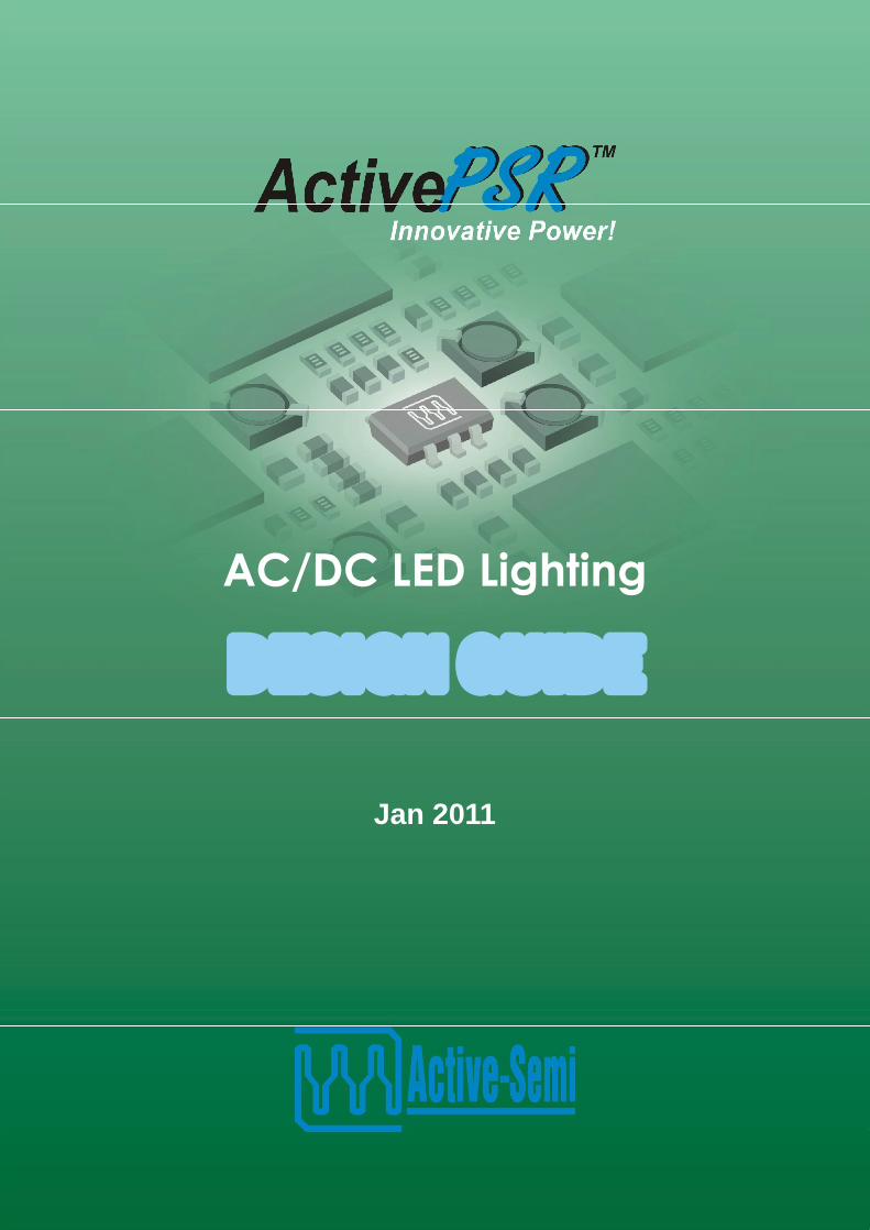
Operation and Application
Figure 1 is the schematic of an offline LED driver using ACT364 to provide a power output of 3.5V, 350mA. This circuit is a typical flyback type power supply which includes the AC rectified circuit (BD1, C1), power drive circuit (BD pin, Q1), secondary rectified circuit (D3, C4) and the IC(ACT364) control circuit. ACT364 is a Primary Side Regulator (PSR) so that the power supply unit can regulate current and voltage without opto-coupler. Pin 4 and Pin 2 are the VDD and ground pins to provide power for the IC. Pin 3 is the base driver for the NPN transistor. Pin 1 is the switching pin. Pin 5 is the feedback pin that senses the output current and output voltage. Pin 6 is the peak current sense pin. Through a patented PSR technology, this circuit
can provide drivers for one (min), or two (max) LED lights in series due to the wide VDD operation ranges.
Key Component Selection
The turn ratio of the primary turn and the secondary turn (NP/NS), together with the R7 sets the maximum output current value as shown in formula (1.1). The voltage setting is through the flyback voltage of auxiliary winding and the feedback resistor R5, R6 as shown in formula (1.2). NP/NS/NAUX (160/10/23) must be designed correctly to make sure it operates in DCM mode and it can supply either one to two LEDs in same circuit. A design value VOUTCV equal to 3.5V and IOUTCC-MIN equal to 350mA are used to do the design.
NS and NAUX are numbers of transformer secondary and auxiliary turns, and VSEC-R is the rectifier diode forward drop voltage at approximately 0.1A bias.
The peak current limit is set by (0.396×0.9) /RCS.
R_SECAUX
S
REFOUTCVV
N
N)
6R5R
1(VV (1.2)
Copyright © 2010 Active-Semi, Inc. - 4 - www.active-semi.com
ACT364 DESIGN GUIDE Innovative PowerTM Sep 2010
Efficiency vs. Input Voltage 70.00
69.20
68.40
67.60
66.80
66.00
AC
T364-001
Effi
cien
cy (
%)
Output Current vs. Input Voltage
340
330
320
310
300
290
280
AC
T364-002
Out
put C
urre
nt (
mA
) Typical performance Characteristics
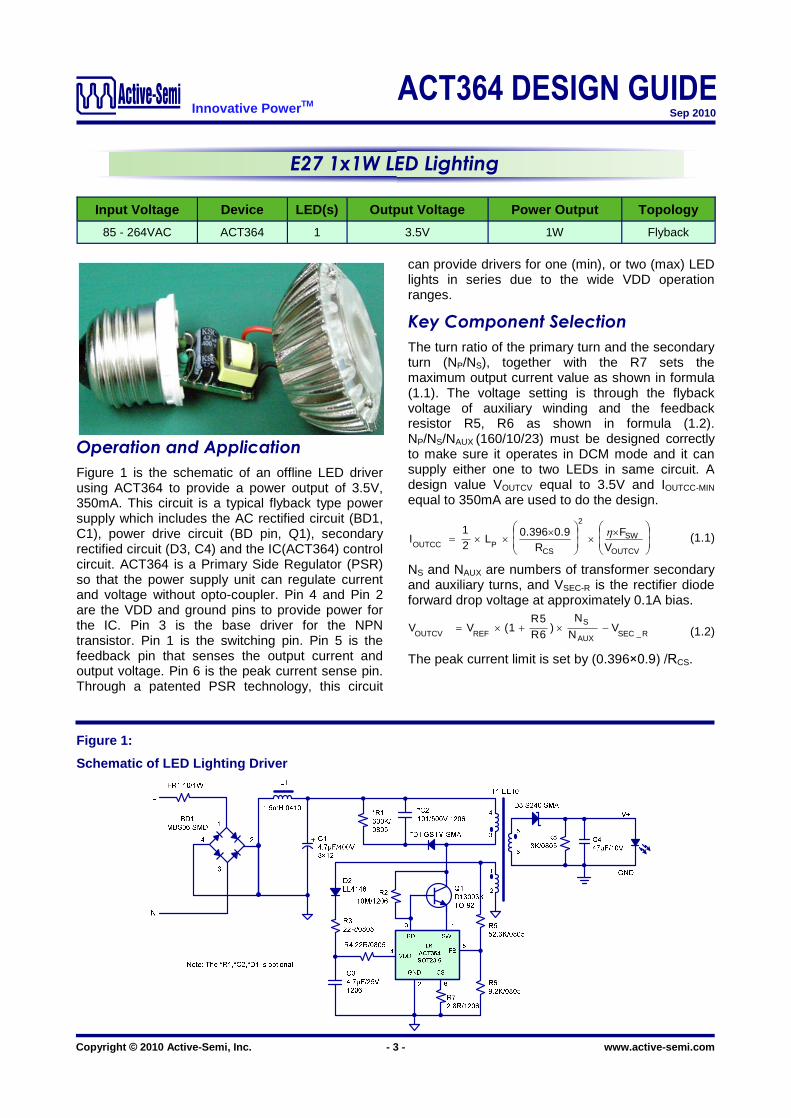
EVALUATION KITS VIN I0 LED(s) ACT364-LED01 85-264VAC 300-350mA 1 or 2
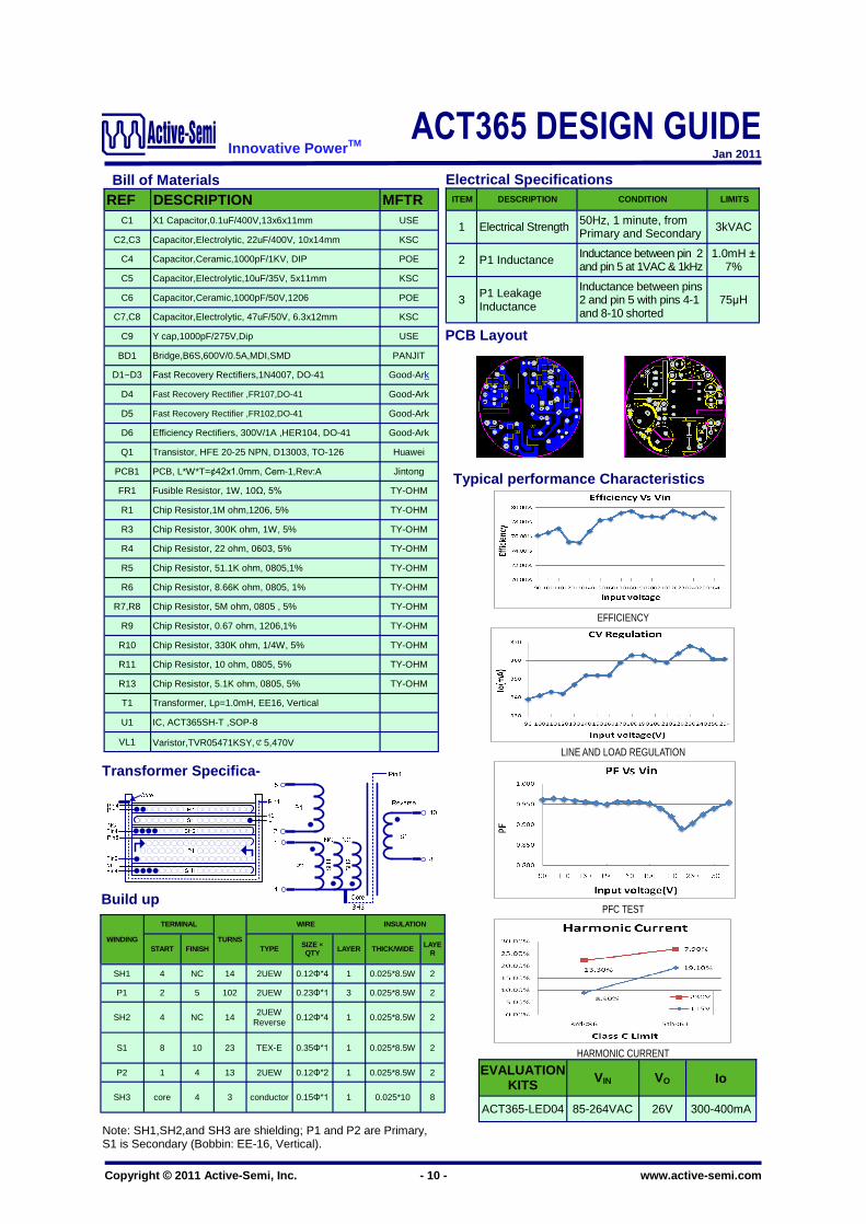
Bill of Materials PCB Top and Bottom Layers
Build Up
WINDING
TERMINAL TURN
S
WIRE INSULATION
START FINISH TYPE SIZE × QTY LAYER THICK/WIDE LAYER
P1 1 4 160 2UEW 0.1Ö×1 3 25µ/8.5mm 2
SH2 2 Open 16 2UEW 0.1Ö×3 1 25µ/8.5mm 2
S1 8 7 10 TEXE
Reverse 0.35Ö×1 1 25µ/8.5mm 2
P2 3 2 23 2UEW 0.1Ö×2 2 25µ/8.5mm 2
SH2 Core 4 1 Copper
Wire 0.18Ö×1 1 25µ/8.5mm 2
REF. DESCRIPTION MFTR.
C1 Capacitor,Electrolytic,4.7µF/400V,8×12mm KSC
C2 Capacitor,Ceramic,100pF/500V,1206,SMD POE
C3 Capacitor,Ceramic,47µF/25V,1206,SMD POE
BD1 Bridge Rectifier,600V/0.5A, MBS06, SDIP PANJIT
D1 Diode,U1tra Fast,GS1M,1000V/1.0A,SMA PANJIT
D2 General Rectifier, LL4148, 100V/1A PANJIT
D3 Diode,schottky,40V/2A,S240,SMA PANJIT
L1 Axial Inductor,1.5mH,0410,Dip SoKa
PCB1 PCB,L*W*T=25.5×14×1.6mm,Rev:A Jintong
FR1 Wire Round Resistor,1W,10ohm,KNP,5% TY-OHM
Q1 Transistor,HFE 15-25,NPN,D13003,TO-92 Huawai
R1 Chip Resistor, 00K ohm,0805,5% TY-OHM
R2 Chip Resistor,10M ohm,1206,5% TY-OHM
R3,4 Chip Resistor,22 ohm,0805,5% TY-OHM
R5 Chip Resistor,52.3K ohm,0805,1% TY-OHM
R6 Chip Resistor,9.2K ohm,0805,1% TY-OHM
R7 Chip Resistor,2.8 ohm,1206,5% TY-OHM
R8 Chip Resistor, 3K ohm, 0805, 5% TY-OHM
T1 Transformer, Lp=4.2mH, EE10
U1 IC, ACT364US-T, SOT23-6 ACT
C4 Capacitor,Ceramic,10µF/10V,1206,SMD POE
Transformer Specification
Note: P1 and P2 are Primary, S1 is Secondary (Bobbin: EE-10 Horizontal).
ITEM DESCRIPTION CONDITION LIMITS
1 Electrical Strength 50Hz, 1 minute, from Primary and Secondary 3kVAC
2 P1 Inductance Inductance between pin 4 and pin 1 at 1VAC & 1kHz
4.2mH ±
7%
3 P1 Leakage Inductance
Inductance between pin 4 and pin 1 with pins 3-2 and 8-5 shorted
75µH
Electrical Specifications
26mm
14mm
115VAC 230VAC
90 110 130 150 170 190 210 230 250
Input Voltage
90 110 130 150 170 190 210 230 250 270
Input Voltage
VIN 85VAC VIN 115VAC VIN 230VAC VIN 264VAC
Copyright © 2010 Active-Semi, Inc. - 5 - www.active-semi.com
ACT364 DESIGN GUIDE Innovative PowerTM Sep 2010
RSECAUX
S
REFOUTCVV
N
N
R
RVV
_)
6
51( (1.2)
OUTCV
SW
2
CSPOUTCC V
FR
9.0396.0L
21
I (1.1)
Input Voltage LED(s) Output Voltage Power Output Topology
85 - 264VAC 1 4V 3W Flyback
Device
ACT364
GU10 1x3W LED Lighting
Figure 1:
Typical Application Circuit
Operation and Application
Figure 1 is the schematic of an offline LED driver using ACT364 to provide a power output of 4V, 650mA. This circuit is a typical flyback type power supply which includes the AC rectified circuit (BD1, L1, C1), primary snubber circuit (D1, R1, C2), power drive circuit (BD pin ,Q1), secondary rectified circuit (D3, C4) and the IC control circuit. ACT364 is a Primary Side Regulator (PSR) so that the power supply unit can regulate current and voltage without Opto-couple. Pin 4 and Pin 2 are the VDD and ground pins to provide power for the IC. Pin 3 is the base drive for the NPN transistor. Pin 1 is the switching pin. Pin 5 is the feedback pin that senses the output current and output voltage. Pin 6 is the peak current sense pin. Through a patented PSR
technology, this circuit can provide drivers one 3W LED lights in series due to the wide VDD operation ranges.
Key Component Selection
The turn ratio of the primary turn and the secondary turn (NP/NS), together with the R7 sets the maximum output current value as shown in formula (1.1). The voltage setting is through the flyback voltage of auxiliary winding and the feedback resistor R5, R6 as shown in formula (1.2). NP/NS/NAUX (168/7/22) must be designed correctly to make sure it operates in DCM mode and it can supply one LEDs in same circuit. A design value VOUTCV equal to 4V and IOUTCC_MIN equal to 650mA are used to do the design.
NS and NAUX are numbers of transformer secondary and auxiliary turns, and VSEC-R is the rectifier diode forward drop voltage at approximately 0.1A bias.
The peak current limit is set by (0.396×0.9) /RCS.

Copyright © 2010 Active-Semi, Inc. - 6 - www.active-semi.com
ACT364 DESIGN GUIDE Innovative PowerTM Sep 2010
Bill of Materials PCB Top and Bottom Layers
Build up
Efficiency vs. Input Voltage
Input Voltage
90 110 130 150 170 190 210 230 250
AC
T364-001
Effi
cien
cy (
%)
Output Current vs. Input Voltage
VOUT1 = 1.8V
AC
T364-002
Out
put C
urre
nt (
mA
)
Transformer Specification
Typical Performance Characteristics
EVALUATION KITS VIN I0 LED(s) ACT364-LED02 85-264VAC 650-750mA 1
P1 and P2 are Primary, S1 is Secondary (Bobbin: EE-10 Vertical)
ITEM DESCRIPTION CONDITION LIMITS
1 Electrical Strength 50Hz, 1 minute, from Primary and Secondary 3kVAC
2 P1 Inductance Inductance between pin 1 and pin 4 at 1VAC & 1kHz
3.2mH ±
7%
3 P1 Leakage Inductance
Inductance between pin 1 and pin 4 with pins 1-2 and 7-8 shorted
75µH
Electrical Specifications
3 LEDs 115VAC 230VAC
85VAC 115VAC 230VAC 264VAC
720
700
680
660
640
620
REF. DESCRIPTION MFTR.
C1 Capacitor,Electrolytic,4.7µF/400V,8×12mm KSC
C2 Capacitor,Ceramic,100pF/500V,1206,SMD POE
C3 Capacitor,Ceramic,4.7µF/25V,1206,SMD POE
BD1 Bridge Rectifier,600V/0.5A,MBS06,SDIP PANJIT
D1 Diode,U1tra Fast,GS1M,1000V/1.0A,SMA PANJIT
D2 General Rectifier,LL4148,100V/1A PANJIT
D3 Diode,schottky,40V/2A,S240,SMA PANJIT
L1 Axial Inductor,1.5mH,0410,Dip SoKa
PCB1 PCB,L*W*T=25.5×14×1.6mm,Rev:A Jintong
FR1 Wire Round Resistor,1W,10ohm,KNP,5% TY-OHM
Q1 Transistor,HFE 15-25,NPN,D13003,TO-92 Huawai
R1 Chip Resistor,300K ohm,0805,5% TY-OHM
R2 Chip Resistor,10M ohm,1206,5% TY-OHM
R3,4 Chip Resistor,22 ohm,0805,5% TY-OHM
R5 Chip Resistor,51.6K ohm,0805,1% TY-OHM
R6 Chip Resistor,9.88K ohm,0805,1% TY-OHM
R7 Chip Resistor,2 ohm,1206,5% TY-OHM
R8 Chip Resistor,2K ohm,0805,5% TY-OHM
T1 Transformer,Lp=3.2mH,EE10
U1 IC,ACT364US-T,SOT23-6 ACT
C4 Capacitor,Ceramic,10µF/10V,1206,SMD POE
WINDING
TERMINAL
TURNS
WIRE INSULATION
START FINISH TYPE SIZE × QTY LAYER THICK/WIDE LAY
ER
P1 1 4 160 2UEW 0.1Ö×1 3 25µ/8.5mm 2
SH2 2 Open 16 2UEW 0.1Ö×3 1 25µ/8.5mm 2
S1 8 7 10 TEXE
Reverse 0.35Ö×1 1 25µ/8.5mm 2
P2 3 2 22 2UEW 0.1Ö×2 2 25µ/8.5mm 2
SH2 Core 4 1 Copper
Wire 0.18Ö×1 1 25µ/8.5mm 2
26mm
14mm
70.00
69.20
68.40
67.60
66.80
66.00
115VAC 230VAC
90 110 130 150 170 190 210 230 250 270
Input Voltage
Copyright © 2010 Active-Semi, Inc. - 7 - www.active-semi.com
ACT364 DESIGN GUIDE Innovative PowerTM Sep 2010
OUTCV
SW
2
CSPOUTCC V
FR
9.0396.0L
21
I (1.1)
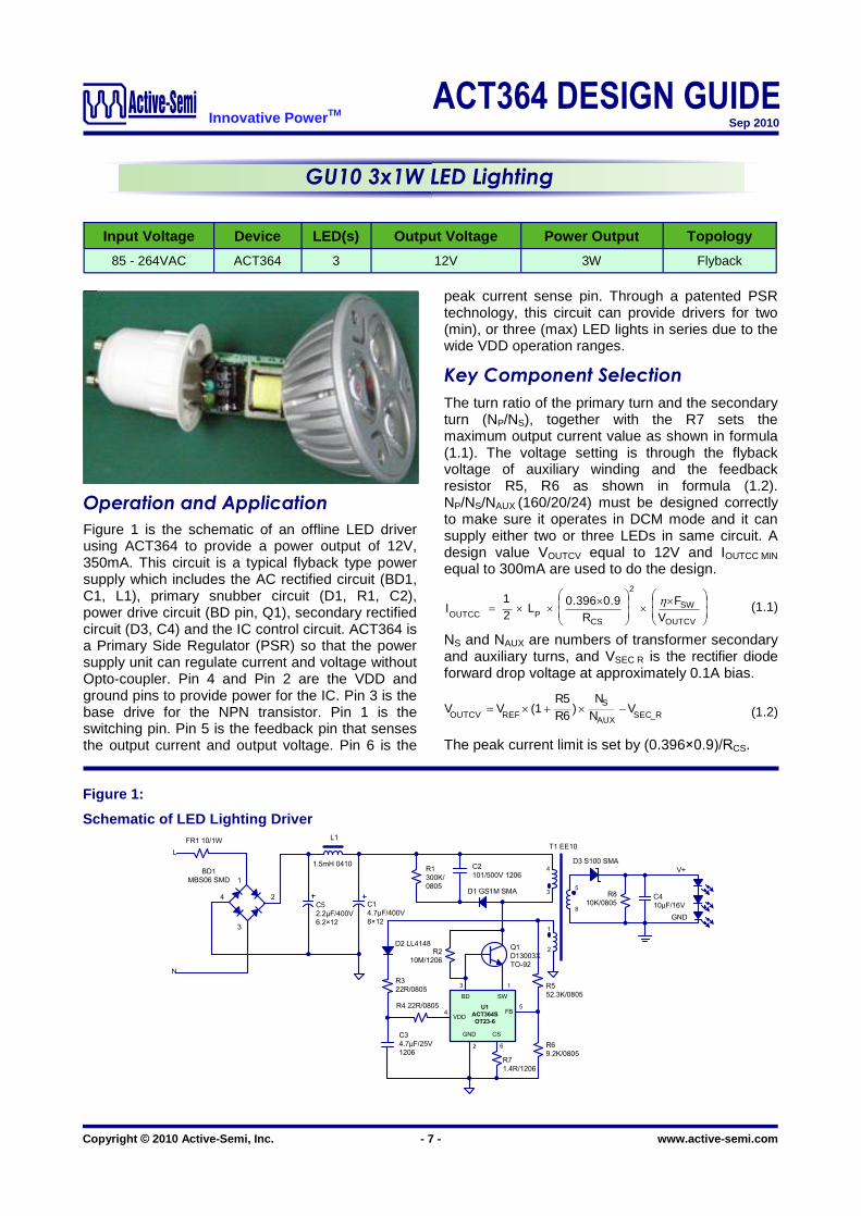
Input Voltage LED(s) Output Voltage Power Output Topology
85 - 264VAC 3 12V 3W Flyback
Device
ACT364
GU10 3x1W LED Lighting
Figure 1:
Schematic of LED Lighting Driver
Operation and Application
Figure 1 is the schematic of an offline LED driver using ACT364 to provide a power output of 12V, 350mA. This circuit is a typical flyback type power supply which includes the AC rectified circuit (BD1, C1, L1), primary snubber circuit (D1, R1, C2), power drive circuit (BD pin, Q1), secondary rectified circuit (D3, C4) and the IC control circuit. ACT364 is a Primary Side Regulator (PSR) so that the power supply unit can regulate current and voltage without Opto-coupler. Pin 4 and Pin 2 are the VDD and ground pins to provide power for the IC. Pin 3 is the base drive for the NPN transistor. Pin 1 is the switching pin. Pin 5 is the feedback pin that senses the output current and output voltage. Pin 6 is the
peak current sense pin. Through a patented PSR technology, this circuit can provide drivers for two (min), or three (max) LED lights in series due to the wide VDD operation ranges.
Key Component Selection
The turn ratio of the primary turn and the secondary turn (NP/NS), together with the R7 sets the maximum output current value as shown in formula (1.1). The voltage setting is through the flyback voltage of auxiliary winding and the feedback resistor R5, R6 as shown in formula (1.2). NP/NS/NAUX (160/20/24) must be designed correctly to make sure it operates in DCM mode and it can supply either two or three LEDs in same circuit. A design value VOUTCV equal to 12V and IOUTCC MIN equal to 300mA are used to do the design.
NS and NAUX are numbers of transformer secondary and auxiliary turns, and VSEC R is the rectifier diode forward drop voltage at approximately 0.1A bias.
The peak current limit is set by (0.396×0.9)/RCS.
R_SECAUX
SREFOUTCV
VNN
)6R5R
1(VV (1.2)
&
)9
7((
/
'660$
5
.
5
.
&
)9
î
&
9
'*6060$
)5:
%'
0%660'
/
1
9''
8
$&76
27
4
';
72
5
0
'//
5
5
5 5
&
)9
5
5
5
.
*1' &6
)%
6:%'
9
*1'
5
.
P+
&
)9
î

Copyright © 2010 Active-Semi, Inc. - 8 - www.active-semi.com
ACT364 DESIGN GUIDE Innovative PowerTM Sep 2010
Bill of Materials PCB Top and Bottom Layers
Build Up
Transformer Specification
Typical Performance Characteristics
EVALUATION KITS VIN I0 LED(s) ACT364-LED03 85-264VAC 280-350mA 2 or 3
Note: P1 and P2 are Primary, S1 is Secondary (Bobbin: EE-10 Vertical).
ITEM DESCRIPTION CONDITION LIMITS
1 Electrical Strength 50Hz, 1 minute, from Primary and Secondary 3kVAC
2 P1 Inductance Inductance between pin 1 and pin 4 at 1VAC & 1kHz
2.1mH ±
7%
3 P1 Leakage Inductance
Inductance between pin 1 and pin 4 with pins 2-3 and 7-8 shorted
75µH
Electrical Specifications
Efficiency vs. Input Voltage
76
74
72
70
68
AC
T364-001
Effi
cien
cy (
%)
230VAC 264VAC 110VAC 85VAC
115VAC 230VAC
Output Current vs. Load 360
320
310
300
290
280
340
330
350
AC
T364-002
Out
put C
urre
nt (
mA
)
REF. DESCRIPTION MFTR.
C1 Capacitor,Electrolytic,4.7µF/400V,8×12mm KSC
C2 Capacitor,Ceramic,100pF/500V,1206,SMD POE
C3 Capacitor,Ceramic,4.7µF/25V,1206,SMD POE
BD1 Bridge Rectifier,600V/0.5A,MBS06,SDIP PANJIT
D1 Diode,U1tra Fast,GS1M,1000V/1.0A,SMA PANJIT
D2 General Rectifier, LL4148, 100V/1A PANJIT
D3 Diode,schottky,100V/1A,S100,SMA PANJIT
L1 Axial Inductor,1.5mH,0410,Dip SoKa
PCB1 PCB,L*W*T=25.5×14×1.6mm,Rev:A Jintong
FR1 Wire Round Resistor,1W,10ohm,KNP,5% TY-OHM
Q1 Transistor,HFE15-25,NPN,D13003,TO-92 Huawai
R1 Chip Resistor,300K ohm,0805,5% TY-OHM
R2 Chip Resistor,10M ohm,1206,5% TY-OHM
R3,4 Chip Resistor,22 ohm,0805,5% TY-OHM
R5 Chip Resistor,52.3K ohm,0805,1% TY-OHM
R6 Chip Resistor,9.2K ohm,0805,1% TY-OHM
R7 Chip Resistor,1.4 ohm,1206,5% TY-OHM
R8 Chip Resistor,10K ohm,0805,5% TY-OHM
T1 Transformer,Lp=2.1mH,EE10
U1 IC, ACT364US-T, SOT23-6 ACT
C4 Capacitor,Ceramic,10µF/16V,1206,SMD POE
C5 Capacitor,Electrolytic,2.2µF/400V,6.2×12mm KSC
26mm
14mm
WINDING
TERMINAL
TURNS
WIRE INSULATION
START FINISH TYPE SIZE × QTY LAYER THICK/WIDE LAY
ER
P1 1 4 160 2UEW 0.1Ö×1 3 25µ/8.5mm 2
SH1 2 Open 16 2UEW 0.1Ö×3 1 25µ/8.5mm 2
S1 8 7 20 TEXE
Reverse 0.25Ö×1 1 25µ/8.5mm 2
P2 3 2 24 2UEW 0.1Ö×2 2 25µ/8.5mm 2
SH2 Core 4 1 Copper
Wire 0.18Ö×1 1 25µ/8.5mm 2
90 110 130 150 170 190 210 230 250
Input Voltage
90 110 130 150 170 190 210 230 250
Input Voltage
230VAC 115VAC
270
264VAC 115VAC 230VAC 85VAC

ACT365 DESIGN GUIDE Innovative PowerTM Jan 2011
Copyright © 2011 Active-Semi, Inc. - 9 - www.active-semi.com
Input Voltage LED(s) Output Voltage Power Output Topology
85 - 264VAC 7 26V 7.8W Flyback
Device
ACT365
Transformer
EE16
PAR30 7x1W LED Lighting
Figure 1:
Schematic of LED Lighting Driver
Operation and Application Figure 1 is the schematic of LED lighting us-
ing ACT365 to provide output power of 26V300mA with PF>0.9.This circuit is a typical flyback power supply which includes the AC rectified circuit(BD1,C1, C2),power drive circuit (BD pin, Q1),power factor rectified circuit (D1-D3,C1,C2),secondary rectified circuit (D6, C7,C8) and the IC control circuit. ACT365 is a Primary Side Regulator (PSR) so that the power supply unit can regulate current and volt-age without Opto-coupler. Pin 4 and Pin 2 are the VDD and ground pins to provide power for the IC. Pin 3 is the base drive for the NPN tran-sistor. Pin 1 is the switching pin. Pin 5 is the feedback pin that senses the output current and output voltage. Pin 6 is the peak current sense pin. Resistance of R10 determines the output DC cord compensation percentage. Through a patented PSR technology, this cir-cuit can provide drivers for five(min), or seven (max) LED lights in series due to the wide VDD operation ranges.
Key Component Selection The maximum output current is decided by formula (1).
(1) Lp is the transformer inductance value, Rcs is the current sense resistor, which is shown as R9 in the schematic. Fsw is the switching
frequency, which design value is 75kHz. is the overall system efficiency, which value is approximately equal to 75%. Voutcc is the output voltage, which setting is through the flyback voltage of auxiliary winding and the feedback resistor R5, R6 as shown in for-mula (2).
(2) Np/Ns/Naux (102/23/13) must be designed correctly to ensure it operates in DCM in all conditions. A design value Voutcc equal to 26V and Ioutcc_min equal to 300mA are used to do the design. Ns and Naux are number of turns of secondary and auxiliary of the transformer. VSEC_R is the forward volt-age drop of the output rectifier diode at ap-proximately 0.1A bias. The peak current limit is set by (0.396×0.9)/Rcs.
)()396.0*9.0
(2
1I 2
OUTCC
SW
CSPOUTCC V
F
RL
RSECAUX
SREFOUTCC V
N
N
R
RV _
6
5 )1(V
ACT365 DESIGN GUIDE Innovative PowerTM Jan 2011
Copyright © 2011 Active-Semi, Inc. - 10 - www.active-semi.com
EVALUATION KITS VIN VO Io
ACT365-LED04 85-264VAC 26V 300-400mA
Bill of Materials
Build up
REF DESCRIPTION MFTR C1 X1 Capacitor,0.1uF/400V,13x6x11mm USE
C2,C3 Capacitor,Electrolytic, 22uF/400V, 10x14mm KSC C4 Capacitor,Ceramic,1000pF/1KV, DIP POE C5 Capacitor,Electrolytic,10uF/35V, 5x11mm KSC C6 Capacitor,Ceramic,1000pF/50V,1206 POE
C7,C8 Capacitor,Electrolytic, 47uF/50V, 6.3x12mm KSC C9 Y cap,1000pF/275V,Dip USE
BD1 Bridge,B6S,600V/0.5A,MDI,SMD PANJIT D1~D3 Fast Recovery Rectifiers,1N4007, DO-41 Good-Ark
D4 Fast Recovery Rectifier ,FR107,DO-41 Good-Ark D5 Fast Recovery Rectifier ,FR102,DO-41 Good-Ark D6 Efficiency Rectifiers, 300V/1A ,HER104, DO-41 Good-Ark Q1 Transistor, HFE 20-25 NPN, D13003, TO-126 Huawei
PCB1 PCB, L*W*T=¢42x1.0mm, Cem-1,Rev:A Jintong FR1 Fusible Resistor, 1W, 10Ω, 5% TY-OHM R1 Chip Resistor,1M ohm,1206, 5% TY-OHM R3 Chip Resistor, 300K ohm, 1W, 5% TY-OHM R4 Chip Resistor, 22 ohm, 0603, 5% TY-OHM R5 Chip Resistor, 51.1K ohm, 0805,1% TY-OHM R6 Chip Resistor, 8.66K ohm, 0805, 1% TY-OHM
R7,R8 Chip Resistor, 5M ohm, 0805 , 5% TY-OHM R9 Chip Resistor, 0.67 ohm, 1206,1% TY-OHM R10 Chip Resistor, 330K ohm, 1/4W, 5% TY-OHM R11 Chip Resistor, 10 ohm, 0805, 5% TY-OHM R13 Chip Resistor, 5.1K ohm, 0805, 5% TY-OHM T1 Transformer, Lp=1.0mH, EE16, Vertical U1 IC, ACT365SH-T ,SOP-8 VL1 Varistor,TVR05471KSY,¢5,470V
Transformer Specifica-
Note: SH1,SH2,and SH3 are shielding; P1 and P2 are Primary, S1 is Secondary (Bobbin: EE-16, Vertical).
ITEM DESCRIPTION CONDITION LIMITS
1 Electrical Strength 50Hz, 1 minute, from Primary and Secondary 3kVAC
2 P1 Inductance Inductance between pin 2 and pin 5 at 1VAC & 1kHz
1.0mH ±
7%
3 P1 Leakage Inductance
Inductance between pins 2 and pin 5 with pins 4-1 and 8-10 shorted
75µH
Electrical Specifications
WINDING
TERMINAL
TURNS
WIRE INSULATION
START FINISH TYPE SIZE × QTY LAYER THICK/WIDE LAYE
R
SH1 4 NC 14 2UEW 0.12Ö*4 1 0.025*8.5W 2 P1 2 5 102 2UEW 0.23Ö*1 3 0.025*8.5W 2
S1 8 10 23 TEX-E 0.35Ö*1 1 0.025*8.5W 2
P2 1 4 13 2UEW 0.12Ö*2 1 0.025*8.5W 2
SH3 core 4 3 conductor 0.15Ö*1 1 0.025*10 8
SH2 4 NC 14 2UEW Reverse 0.12Ö*4 1 0.025*8.5W 2
Typical performance Characteristics
PCB Layout
EFFICIENCY
LINE AND LOAD REGULATION
PFC TEST
HARMONIC CURRENT

ACT50 DESIGN GUIDE Innovative PowerTM June 2010
Copyright © 2010 Active-Semi, Inc. - 11 - www.active-semi.com
9R13R)T(14R13R)T(14R
10RIVoBE
(1)
FEATURES Universal AC input
High efficiency
Constant Voltage Control & Short Circuit Protection
CC temperature compensation
±5% current accuracy
Exceed Energy Start 2.0 regulation
Small SOT23-5 Package
APPLICATIONS
Off-Line isolated LED Driver
Operation and Application
Figure 1 is the schematic of an offline LED driver using ACT50 to provide a power output of 16V, 350mA. This circuit is a Flyback type power supply which includes the AC rectified circuit (D4, L1, C1, C2), power drive circuit (D9, R6, Q1), output rectified circuit (D10, C8) and the IC supply and control circuit. ACT50 is a very low cost peak
current control PWM controller. Constant voltage control is through OPTO couple and ZD1. Accurate current control is through R10 and the TC compensation circuit (C9, R14, R13).
Key Component Selection
The inductance value is selected to enable to operate the circuit in the CCM mode. The ripple current can be designed to be 20%-40% of the load current. A fast efficiency rectifier D10 is required to achieve higher efficiency. The turn ratio of secondary and auxiliary can be set as to make sure the VDD in a working range. The serial output voltage V0 should be in the range of 12V-16V voltage. The constant output current is set through R10 according formula (1). R14 is a thermal resistor to achieve good output current accuracy in high temperature. VBE is 0.6V at 25°C and 0.55V at 50°C
respectively.
ZD1 is selected to set the output voltage constant when it is in open circuit.
Figure 1:
Typical Application Circuit
Input Voltage LED(s) Output Voltage Power Output Topology
85 - 264VAC 4 16V 5W Flyback
Device
ACT50
16V, 5W, 350mA High Efficiency Solutions
='
9&
S)
9
W
5
ȍ
5
17&Nȍ
5Nȍ
5
ȍ
4
.7&
,&%
(/
5
Nȍ
&
)
9
5ȍ
&
S)
,&$
(/5
Nȍ
6:
9''
,6(7 *1'
)%,&
$&78&
'1
5ȍ&
S)
9
&
)9
5
ȍ
4
';
7((
5
Nȍ
5
Nȍ
&
)
9
5Nȍ
/P+
&
)
9
'
)5
'
1
)
$9
99$&
&
S)
N9
&
S)9
5ȍ
'
6%
<&
S)9
5
Nȍ
959
/('
/('
/('
/('
'//
ACT50 DESIGN GUIDE Innovative PowerTM June 2010
Copyright © 2010 Active-Semi, Inc. - 12 - www.active-semi.com
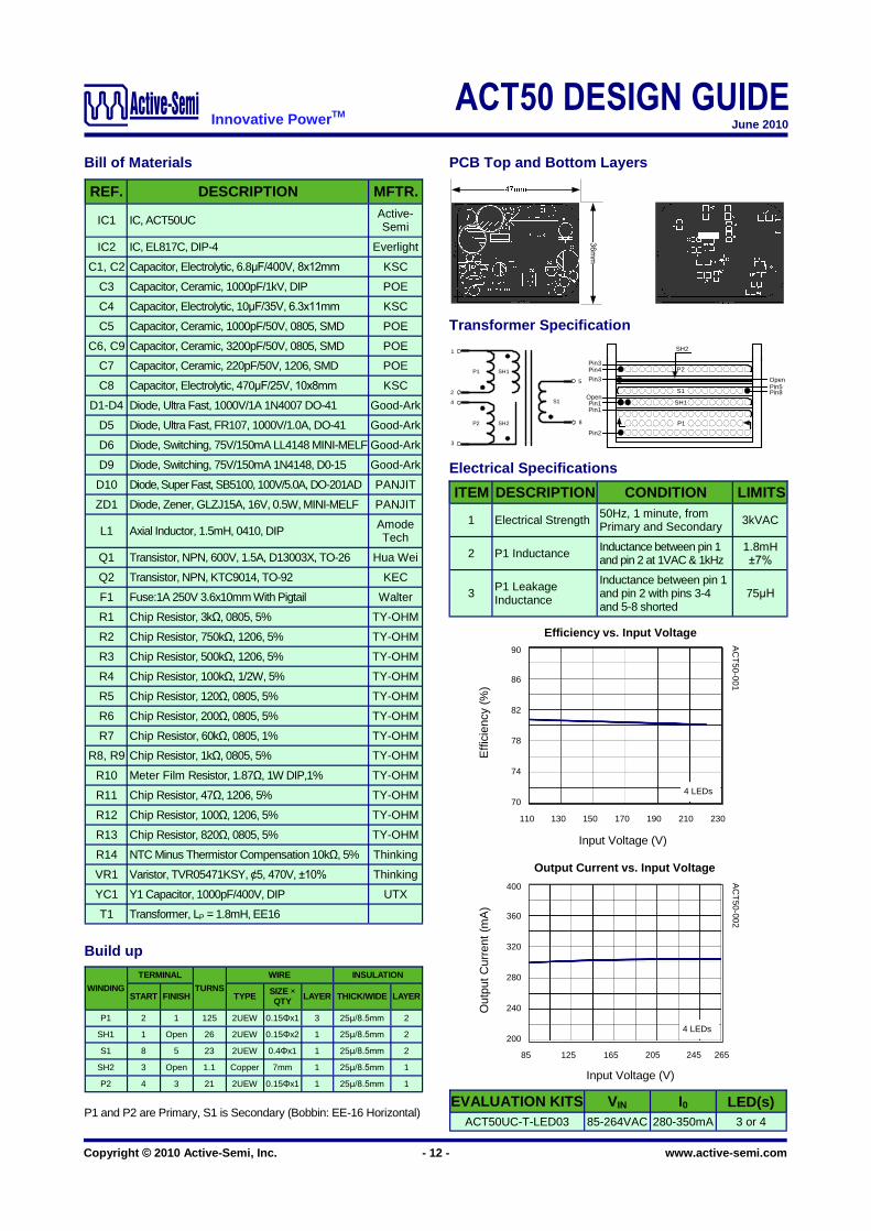
Bill of Materials PCB Top and Bottom Layers
Build up
REF. DESCRIPTION MFTR.
IC1 IC, ACT50UC Active-Semi
IC2 IC, EL817C, DIP-4 Everlight
C1, C2 Capacitor, Electrolytic, 6.8µF/400V, 8x12mm KSC
C3 Capacitor, Ceramic, 1000pF/1kV, DIP POE
C4 Capacitor, Electrolytic, 10µF/35V, 6.3x11mm KSC
C5 Capacitor, Ceramic, 1000pF/50V, 0805, SMD POE
C6, C9 Capacitor, Ceramic, 3200pF/50V, 0805, SMD POE
C7 Capacitor, Ceramic, 220pF/50V, 1206, SMD POE
C8 Capacitor, Electrolytic, 470µF/25V, 10x8mm KSC
D1-D4 Diode, Ultra Fast, 1000V/1A 1N4007 DO-41 Good-Ark
D5 Diode, Ultra Fast, FR107, 1000V/1.0A, DO-41 Good-Ark
D6 Diode, Switching, 75V/150mA LL4148 MINI-MELF Good-Ark
D9 Diode, Switching, 75V/150mA 1N4148, D0-15 Good-Ark
D10 Diode, Super Fast, SB5100, 100V/5.0A, DO-201AD PANJIT
ZD1 Diode, Zener, GLZJ15A, 16V, 0.5W, MINI-MELF PANJIT
L1 Axial Inductor, 1.5mH, 0410, DIP Amode Tech
Q1 Transistor, NPN, 600V, 1.5A, D13003X, TO-26 Hua Wei
Q2 Transistor, NPN, KTC9014, TO-92 KEC
F1 Fuse:1A 250V 3.6x10mm With Pigtail Walter
R1 Chip Resistor, 3kÙ, 0805, 5% TY-OHM
R2 Chip Resistor, 750kÙ, 1206, 5% TY-OHM
R3 Chip Resistor, 500kÙ, 1206, 5% TY-OHM
R4 Chip Resistor, 100kÙ, 1/2W, 5% TY-OHM
R5 Chip Resistor, 120Ù, 0805, 5% TY-OHM
R6 Chip Resistor, 200Ù, 0805, 5% TY-OHM
R7 Chip Resistor, 60kÙ, 0805, 1% TY-OHM
R8, R9 Chip Resistor, 1kÙ, 0805, 5% TY-OHM
R10 Meter Film Resistor, 1.87Ù, 1W DIP,1% TY-OHM
R11 Chip Resistor, 47Ù, 1206, 5% TY-OHM
R12 Chip Resistor, 100Ù, 1206, 5% TY-OHM
R13 Chip Resistor, 820Ù, 0805, 5% TY-OHM
R14 NTC Minus Thermistor Compensation 10kÙ, 5% Thinking
VR1 Varistor, TVR05471KSY, ¢5, 470V, ±10% Thinking
YC1 Y1 Capacitor, 1000pF/400V, DIP UTX
T1 Transformer, LP = 1.8mH, EE16
WINDING
TERMINAL
TURNS
WIRE INSULATION
START FINISH TYPE SIZE × QTY LAYER THICK/WIDE LAYER
P1 2 1 125 2UEW 0.15Öx1 3 25µ/8.5mm 2
SH1 1 Open 26 2UEW 0.15Öx2 1 25µ/8.5mm 2
S1 8 5 23 2UEW 0.4Öx1 1 25µ/8.5mm 2
SH2 3 Open 1.1 Copper 7mm 1 25µ/8.5mm 1
P2 4 3 21 2UEW 0.15Öx1 1 25µ/8.5mm 1
ITEM DESCRIPTION CONDITION LIMITS
1 Electrical Strength 50Hz, 1 minute, from Primary and Secondary 3kVAC
2 P1 Inductance Inductance between pin 1 and pin 2 at 1VAC & 1kHz
1.8mH ±7%
3 P1 Leakage Inductance
Inductance between pin 1 and pin 2 with pins 3-4 and 5-8 shorted
75µH
PP
Efficiency vs. Input Voltage
VOUT1 = 1.8V 90
86
82
78
74
70
Input Voltage (V)
110 130 150 230 170 190 210
AC
T50-001
Effi
cien
cy (
%)
Output Current vs. Input Voltage
VOUT1 = 1.8V 400
360
320
280
240
200
Input Voltage (V)
85 125 165 205 245 265
AC
T50-002
Out
put C
urre
nt (
mA
)
S1
5
8
P1
1
2
P2
3
4
SH1
SH2
Pin8Pin5
Pin3
Pin2
Pin1Pin1
Pin4
P1
SH1
S1
P2
Open
SH2
Pin3
Open
Transformer Specification
Electrical Specifications
EVALUATION KITS VIN I0 LED(s) ACT50UC-T-LED03 85-264VAC 280-350mA 3 or 4
4 LEDs
4 LEDs
P1 and P2 are Primary, S1 is Secondary (Bobbin: EE-16 Horizontal)

ACT50 DESIGN GUIDE Innovative PowerTM June 2010
Copyright © 2010 Active-Semi, Inc. - 13 - www.active-semi.com
FEATURES Universal AC input
High Efficiency
Constant Voltage Control & Short Circuit Protection
CC Temperature Compensation
±5% Current Accuracy
Exceed Energy Start 2.0 Regulation
Small SOT23-5 Package
APPLICATIONS
Off-Line isolated LED Driver
Operation and Application
Figure 1 is the schematic of an offline LED driver using ACT50 to provide a power output of 49V, 128mA. This circuit is a flyback type power supply which includes the AC rectified circuit (D4, L1, C1, C2), power drive circuit (D9, R6, Q1), output rectified circuit (D10, C8) and the IC supply and control circuit. ACT50 is a very low cost peak
current control PWM controller. Constant voltage control is through OPTO couple and ZD1. Accurate current control is through R10 and the TC compensation circuit (R9, R13, R14).
Key Component Selection
The inductance value is selected to enable to operate the circuit in the CCM mode. The ripple current can be designed to be 20%-40% of the load current. A fast efficiency rectifier D10 is required to achieve higher efficiency. The turn ratio of secondary and auxiliary can be set as to make sure the VDD in a working range. The serial output voltage V0 should be in the range of 48V-52V voltage. The constant output current is set through R10 according formula (1). R14 is a thermal resistor to achieve good output current accuracy in high temperature. VBE is 0.6V at 25°C and 0.55V at 50°C
respectively.
ZD1 is selected to set the output voltage constant when it is in open circuit.
Figure 1:
Typical Application Circuit
49V, 5W, 128mA High Efficiency Solutions
='
9 &
S)
9
W
5
ȍ
5
17&
Nȍ
5Nȍ
5
ȍ
4
.7&
,&%
(/
5
Nȍ
&
)9
/('
5ȍ
'
+(5
&
S),&$
(/5
Nȍ
6:
9''
,6(7 *1'
)%,&
$&78&
'//
5ȍ&
S)9
&
)9
5
ȍ
4
';
7((
5
Nȍ
5
Nȍ
&
)
9
5Nȍ
/P+
&
)
9
'
)5
'
',6
)
$9
99$&
&
S)N9
&
S)9
5ȍ
'
%<
5
Nȍ
&
S)9
5
Nȍ
1/
'//
9R13R)T(14R13R)T(14R
10RIV 0BE
(1)
Input Voltage LED(s) Output Voltage Power Output Topology
85 - 264VAC 14 Serial LED × 8 Line 49V 5W Flyback
Device
ACT50

ACT50 DESIGN GUIDE Innovative PowerTM June 2010
Copyright © 2010 Active-Semi, Inc. - 14 - www.active-semi.com
50mm
19m
m
Bill of Materials PCB Top and Bottom Layers
EVALUATION KITS VIN I0 LED(s)
ACT50UC-T-LED05 85-264VAC 115-140mA 14s x 8p (8x16mA)
Build Up
REF. DESCRIPTION MFTR. IC1 IC, ACT50UC-T, SOT23-5 Active
IC2 IC, EL817C, DIP-4 Everlight
C1 Capacitor, Electrolytic, 6.8µF/400V, 10×12mm KSC
C2 Capacitor, Electrolytic, 4.7µF/400V, 8×12mm KSC
C3 Capacitor, Ceramic, 1000pF/1kV, DIP POE
C4 Capacitor, Electrolytic, 10µF/35V, 5×11mm KSC
C5 Capacitor, Ceramic, 1000pF/50V, 0805, SMD POE
C6 Capacitor, Ceramic, 3300pF/50V, 0805, SMD POE
C7 Capacitor, Ceramic, 220pF/50V, 1206, SMD POE
C8 Capacitor, Electrolytic, 100µF/63V, 8×12mm KSC
C9 Capacitor, Ceramic, 1000pF/50V, 0603, SMD POE
C10 Safety Capacitor, Y2, 1000pF/400V, DIP UTX
D4 Bridge Rectifier, 1000V/1A DI1010S, SDIP PANJIT
D5 Diode, Ultra Fast, FR107, 1000V/1.0A, DO-41 Good-Ark
D8, D9 Diode, Switching, 75V/150mA LL4148 MINI-MELF Good-Ark
D10 Diode, Super Fast, BY299, 800V/2.0A, DO-201AD PANJIT
ZD1 Diode, Zener, GLZ47, 47V, 0.5W, MINI-MELF Good-Ark
L1 Axial Inductor, 1.5mH, 0410, DIP Amode Tech
Q1 Transistor, NPN, 600V, 1.5A, D13003X, TO-126 Hua Wei
Q2 Transistor, NPN, KTC9014, TO-92 KEC
F1 Fuse: 1A 250V 3.6×10mm With Pigtail Walter
R1 Meter Film Resistor, 3kÙ, 0805, 5% TY-OHM
R2 Chip Resistor, 750kÙ, 1206, 5% TY-OHM
R3 Chip Resistor, 500kÙ, 0805, 5% TY-OHM
R4 Chip Resistor, 100kÙ, 1206, 5% TY-OHM
R5 Chip Resistor, 10Ù, 0805, 5% TY-OHM
R6 Chip Resistor, 200Ù, 0805, 5% TY-OHM
R7 Chip Resistor, 60kÙ, 0805, 1% TY-OHM
R8 Chip Resistor, 3.9kÙ, 0805, 5% TY-OHM
R9 Chip Resistor, 1kÙ, 0805, 5% TY-OHM
R10 Meter Film Resistor, 1.87Ù, 1/2W DIP, 1% TY-OHM
R11 Chip Resistor, 47Ù, 1206, 5% TY-OHM
R12 Chip Resistor, 100Ù, 1206, 5% TY-OHM
R13 Chip Resistor, 820Ù, 0603, 5% TY-OHM
R14 NTC Minus Thermistor Compensation 10kÙ, 5% Thinking
R15 Chip Resistor, 91kÙ, 0603, 5% TY-OHM
T1 Transformer, LP = 2.0mH, EE-16
D6 Diode, Ultra Fast, HER103, 200V/1.0A, DO-41 Good-Ark
WINDING
TERMINAL
TURNS
WIRE INSULATION
START FINISH TYPE SIZE × QTY LAYER THICK/WIDE LAYER
SH1 1 Open 26 2UEW 0.15Ö×2 1 25µ/8.5mm 2
P1 2 1 125 2UEW 0.15Ö×1 3 25µ/8.5mm 2
SH2 3 Open 26 2UEW 0.15Ö×2 1 25µ/8.5mm 2
S1 8 7 68 TEXE 0.3Ö×1 1 25µ/8.5mm 2
P2 4 3 21 2UEW 0.15Ö×1 1 25µ/8.5mm 3
SH3 3 Open 1.1 Copper 7mm 1 25µ/8.5mm 3
ITEM DESCRIPTION CONDITION LIMITS
1 Electrical Strength 50Hz, 1 minute, from Primary and Secondary 3kVAC
2 P1 Inductance Inductance between pin 1 and pin 2 at 1VAC & 1kHz
2.0mH ±7%
3 P1 Leakage Inductance
Inductance between pin 1 and pin 2 with pins 3-4 and 7-8 shorted
75µH
Efficiency vs. Input Voltage 90
86
82
78
74
70
AC
T50-001
Effi
cien
cy (
%)
Output Current vs. Input Voltage 160
140
120
100
AC
T50-002
Out
put C
urre
nt L
oad
(mA
)
Transformer Specification
Electrical Specifications
Input Voltage (V)
85 125 165 205 245 265
14s x 8p LEDs
Input Voltage (V)
85 125 165 205 245 265
14s x 8p LEDs
Typical Performance Characteristics
P1 and P2 are Primary, S1 is Secondary (Bobbin: EE-16 Horizontal)
Pin1
Pin8
SH1
Pin7Pin4
Pin2
Pin1Pin3
Pin3
P1
SH2
S1
P2
SH3
Pin3 Open
8
S1
7
P1
1
2
P2
3
4
SH1
SH2
SH
3
ACT50 DESIGN GUIDE Innovative PowerTM June 2010
Copyright © 2010 Active-Semi, Inc. - 15 - www.active-semi.com
15R12R1RT15R1RT
14R13R14R13R
IV0BE
(1)
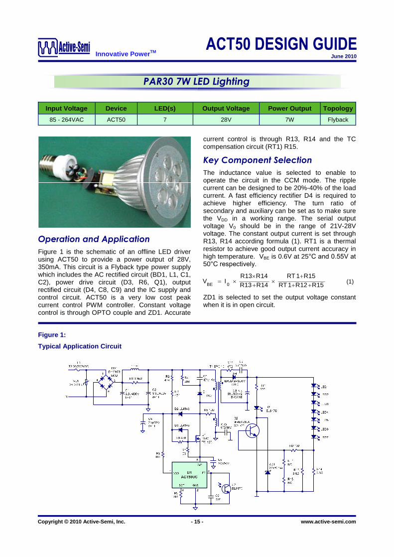
PAR30 7W LED Lighting
Figure 1:
Typical Application Circuit
Operation and Application
Figure 1 is the schematic of an offline LED driver using ACT50 to provide a power output of 28V, 350mA. This circuit is a Flyback type power supply which includes the AC rectified circuit (BD1, L1, C1, C2), power drive circuit (D3, R6, Q1), output rectified circuit (D4, C8, C9) and the IC supply and control circuit. ACT50 is a very low cost peak current control PWM controller. Constant voltage control is through OPTO couple and ZD1. Accurate
current control is through R13, R14 and the TC compensation circuit (RT1) R15.
Key Component Selection
The inductance value is selected to enable to operate the circuit in the CCM mode. The ripple current can be designed to be 20%-40% of the load current. A fast efficiency rectifier D4 is required to achieve higher efficiency. The turn ratio of secondary and auxiliary can be set as to make sure the VDD in a working range. The serial output voltage V0 should be in the range of 21V-28V voltage. The constant output current is set through R13, R14 according formula (1). RT1 is a thermal resistor to achieve good output current accuracy in high temperature. VBE is 0.6V at 25°C and 0.55V at
50°C respectively.
ZD1 is selected to set the output voltage constant when it is in open circuit.
Input Voltage LED(s) Output Voltage Power Output Topology
85 - 264VAC 7 28V 7W Flyback
Device
ACT50

ACT50 DESIGN GUIDE Innovative PowerTM June 2010
Copyright © 2010 Active-Semi, Inc. - 16 - www.active-semi.com
346
Bill of Materials PCB Layout
Efficiency vs. Input Voltage 82
79
78
77
76
75
81
80
AC
T50-001
Effi
cien
cy (
%)
Transformer Specification
Electrical Specifications
7 LEDs
Input Voltage (V)
85 125 165 205 245 265
Output Current vs. Input Voltage
340
328
316
304
292
280
AC
T50-002
Out
put C
urre
nt (
mA
)
Input Voltage (V)
85 125 165 205 245 265
Build up
EVALUATION KITS VIN I0 LED(s) ACT50UC-T-LED04 85-264VAC 280-350mA 7
REF DESCRIPTION MFTR U1 IC, ACT50UC, SOT23-5 Active U2 IC, EL817C, DIP-4 Everlight
C1, C2 Capacitor Electrolytic, 3.3µF/400V, 8×12mm KSC C3 Capacitor Ceramic, 470pF/1KV, DIP POE C4 Capacitor Electrolytic, 22µF/35V, 5×11mm KSC C5 Capacitor Ceramic,1000pF/50V,0805 POE C6 Capacitor Ceramic, 3300pF/25V,0603 POE
C7 Capacitor Ceramic, 220pF/50V,0805 POE C8, C9 Capacitor Tantalum, 33µF/35V, D Case AVX
C10 Capacitor Ceramic,1000pF/1KV, DIP POE BD1 Bridge Rectifier,1000V/1A, DI1010S, SDIP PANJIT D1 Diode, Ultra Fast, FR107, 1000V/1.0A, DO-41 Good-Ark
D2 Diode, Switching, 75V/150mA, LL4148, MICRO-MELF Good-Ark
D3 Diode, Switching, 75V/150mA, LL4148, MICRO-MELF Good-Ark
D4 Diode, Ultra Fast, ER2D, 200V/2.0A, SMD PANJIT
ZD1 Diode, Zener, GMZJ27A ,27V, 0.5W, MICRO-MELF PANJIT
Q1 Transistor, Mosfet, 1N60, TO-126 UTC Q2 Amplifier Transistor, NPN, MMBT3904, SOT-23
F1 Fuse: 2.0A 250V 3.6 × 10mm With Pigtail,
Ceramic tube Walter
L1 Axial Inductor, 1mH, 0410, DIP Amode Tech
PCB1 ACT50 PCB, Ö18mm, T = 1.6mm, CEM-1, Rev: A Jintong
PCB2 ACT50 PCB, L × W × T = 29 × 28 × 1.0mm, FR-4, Rev: A Jintong
R1 Chip Resistor, 1.5kÙ,1206, 5% TY-OHM R2 Chip Resistor, 470kÙ,1206, 5% TY-OHM R3 Chip Resistor, 470kÙ,1206, 5% TY-OHM R4 Chip Resistor, 300kÙ,1206, 5% TY-OHM
R5 Chip Resistor, 10Ù,1206, 5% TY-OHM R6 Chip Resistor, 47Ù,0805, 5% TY-OHM R7 Chip Resistor, 10kÙ,0805, 5% TY-OHM R8 Chip Resistor, 100Ù,0805, 5% TY-OHM R9 Chip Resistor, 39kÙ,0603, 1% TY-OHM R10 Chip Resistor, 47Ù,1206, 5% TY-OHM R11 Chip Resistor, 2.0kÙ,0603, 5% TY-OHM R12 Chip Resistor, 1kÙ,0603, 5% TY-OHM
R13, R14 Chip Resistor, 3.6Ù,1206, 1% TY-OHM
R15 NC TY-OHM RT1 NC Thinking T1 Transformer, LP = 1.8mH, EPC-19
VR1 Varistor, TVR05431KSY, ¢5, 430V, ±10%, DIP Thinking
WINDING TERMINAL
TURNS WIRE INSULATION
START FINISH TYPE SIZE × QTY LAYER THICK/WIDE LAYER
P1 3 1 95 2UEW 0.25Ö×1 1 25µ/8.5mm 2
SH1 4 Open 40 2UEW 0.15Ö×2 1 25µ/8.5mm 2
S1 11 10 40 TEXE 0.45Ö×1 1 25µ/8.5mm 2
SH2 4 Open 0.9 Copper 7mm 1 25µ/8.5mm 2
P2 5 4 20 2UEW 0.15Ö×2 1 25µ/8.5mm 2
SH3 4 Open 1.1 Copper 7mm
(Epiboly) 1 25µ/8.5mm 2
ITEM DESCRIPTION CONDITION LIMITS
1 Electrical Strength 50Hz, 1 minute, from primary and secondary 3kVAC
2 P1 Inductance Inductance between pins 1 and 3 at 1VAC & 1kHz
1.8mH ±7%
3 P1 Leakage Inductance
Inductance between pins 1 and 3 with pins 5-4 and 11-10 shorted
75µH
7 LEDs
P1 and P2 are Primary, S1 is Secondary (Bobbin: EPC19 Horizontal)
P1
P2
5
4
3
1
SH2
S1
11
10SH3SH1
Pin3
Pin10
Pin1SH1
S1Open
Pin4
P1
P2
Pin11
Pin4
Pin4
Pin5
Pin4
SH2 SH3

ACT50 DESIGN GUIDE Innovative PowerTM June 2010
Copyright © 2010 Active-Semi, Inc. - 17 - www.active-semi.com
FEATURES Universal AC input
High efficiency
Constant Voltage Control & Short Circuit Protection
CC temperature compensation
±5% current accuracy
Exceed Energy Start 2.0 regulation
Small SOT23-5 Package
APPLICATIONS
Off-Line Non-isolated LED Driver
Operation and Application
Figure 1 is the schematic of an offline LED driver using ACT50 to provide a power output of 35V, 350mA. This circuit is a buck type power supply which includes the AC rectified circuit (BD1, L1, C1, C2), power drive circuit (D9, R6, Q1), output rectified circuit (D10, C8, C9) and the IC supply and control circuit. ACT50 is a very low cost peak
current control PWM controller. Constant voltage control is through OPTO couple and ZD1. Accurate current control is through R10 and the TC compensation circuit (R9, R14, R13).
Key Component Selection
The inductance value is selected to enable to operate the circuit in the CCM mode. The ripple current can be designed to be 20%-40% of the load current. A fast efficiency rectifier D10 is required to achieve higher efficiency. The turn ratio of primary and auxiliary can be set as to make sure the VDD in a working range. The serial output voltage V0 should be in the range of 35V-40V voltage. The constant output current is set through R10 according formula (1). R14 is a thermal resistor to achieve good output current accuracy in high temperature. VBE is 0.6V at 25°C and 0.55V at 50°C
respectively.
ZD1 is selected to set the output voltage constant when it is in open circuit.
Figure 1:
Typical Application Circuit
35V, 12W, 350mA High Efficiency Solutions
9R13R)T(14R
13R)T(14R10RIV oBE
(1)
Input Voltage LED(s) Output Voltage Power Output Topology
85 - 264VAC 10 35V 12W Buck
Device
ACT50

ACT50 DESIGN GUIDE Innovative PowerTM June 2010
Copyright © 2010 Active-Semi, Inc. - 18 - www.active-semi.com
Bill of Materials PCB Top and Bottom Layers
EVALUATION KITS VIN I0 LED(s) ACT50UC-T-LED11 85-264VAC 280-350mA 9 or 10
Build up
REF. DESCRIPTION MFTR.
IC1 IC, ACT50UC Active-Semi
IC2 IC, EL817C, DIP-4 Everlight
C1, C2 Capacitor, Electrolytic, 10µF/400V, 8x12mm KSC
C4 Capacitor, Electrolytic, 22µF/35V, 5x11mm KSC
C5 Capacitor, Ceramic, 1000pF/50V, 0805, SMD POE
C6, C10 Capacitor, Ceramic, 3300pF/50V, 0805, SMD POE
C8, C9 Capacitor, Electrolytic, 100µF/50V, 8x12mm KSC
BD1 Bridge Rectifier, 1000V/1A, DI1010S, SDIP Good-Ark
D6 Diode, Super Fast, HER103, 200V/1.0A, DO-41 PANJIT
D9 Diode, Switching, 75V/150mA 1N4148, DIP Good-Ark
D10 Fast Efficient Rectifier, BYV26B, 500V/1A, DO-204AP
GS
ZD1 Diode, Zener, GLZ39A, 39V, 0.5W, MINI-MELF Good-Ark
L1 Axial Inductor, 300µH, 0410, DIP Amode Tech
Q1 Transistor, NPN, 600V, 1.5A, D13003X, TO-126 Hua Wei
Q2 Transistor, NPN, KTC9014, TO-92 KEC
F1 Fuse: 1A 250V 3.6 x 10mm With Pigtail Walter
R1 Chip Resistor, 3kÙ, 0805, 5% TY-OHM
R2 Chip Resistor, 750kÙ, 1206, 5% TY-OHM
R3 Chip Resistor, 750kÙ, 1206, 5% TY-OHM
R5 Chip Resistor, 10Ù, 0805, 5% TY-OHM
R6 Chip Resistor, 200Ù, 0805, 5% TY-OHM
R7 Chip Resistor, 39kÙ, 0805, 1% TY-OHM
R8 Chip Resistor, 6kÙ, 0805, 5% TY-OHM
R9 Chip Resistor, 1kÙ, 0805, 5% TY-OHM
R10 Film Resistor, 1.87Ù, 1/2W DIP,1% TY-OHM
R12 Chip Resistor, 100Ù, 1206, 5% TY-OHM
R13 Chip Resistor, 820Ù, 0603, 5% TY-OHM
R14 NTC Minus Thermistor Compensation 10kÙ, 5% Thinking
T1 Transformer, LP = 2.6mH, EE-19
VR1 Varistor, TVR05471KSY, ¢5, 470V, ±10% Thinking
WINDING
TERMINAL
TURNS
WIRE INSULATION
START FINISH TYPE SIZE × QTY LAYER THICK/WIDE LAYER
P1 2 1 143 2UEW 0.3Ö×1 1 25µ/8.5mm 2
SH2 1 Open 30 2UEW 0.15Ö×2 1 25µ/8.5mm 2
P2 4 3 55 2UEW 0.15Ö×1 1 25µ/8.5mm 3
Transformer Specification
Electrical Specifications
ITEM DESCRIPTION CONDITION LIMITS
1 Electrical Strength 50Hz, 1 minute, from Primary and Secondary 3kVAC
2 P1 Inductance Inductance between pins 1 and 2 at 1VAC & 1kHz
2.6mH ±7%
3 P1 Leakage Inductance
Inductance between pin 1 and pin 2 with pins 3-4 shorted
75µH
P1 and P2 are Primary, P2 is Secondary (Bobbin: EE-19 Horizontal)
Typical Performance Characteristics
Output Current vs. Input Voltage
VOUT1 = 1.8V 400
370
340
310
280
Input Voltage (V)
85 125 165 205 245 265
AC
T50-002
Out
put C
urre
nt L
oad
(mA
)
10 LEDs
Effi
cien
cy (
%)
Efficiency vs. Input Voltage
AC
T50-001
10 LEDs
Input Voltage (V)
85 125 165 205 245 265
92
88
84
80
94
P1
P2
4
3
SH1
2
1Pin3
Pin2
Pin1Pin1
P1
SH1
P2OpenPin4
ACT50 DESIGN GUIDE Innovative PowerTM June 2010
Copyright © 2010 Active-Semi, Inc. - 19 - www.active-semi.com
17R16R1RT17R1RT
15R14R15R14R
IV oBE
(1)
Input Voltage LED(s) Output Voltage Power Output Topology
85 - 264VAC 12 42V 12W Flyback
Device
ACT50
PAR38 12W LED Lighting
Figure 1:
Typical Application Circuit
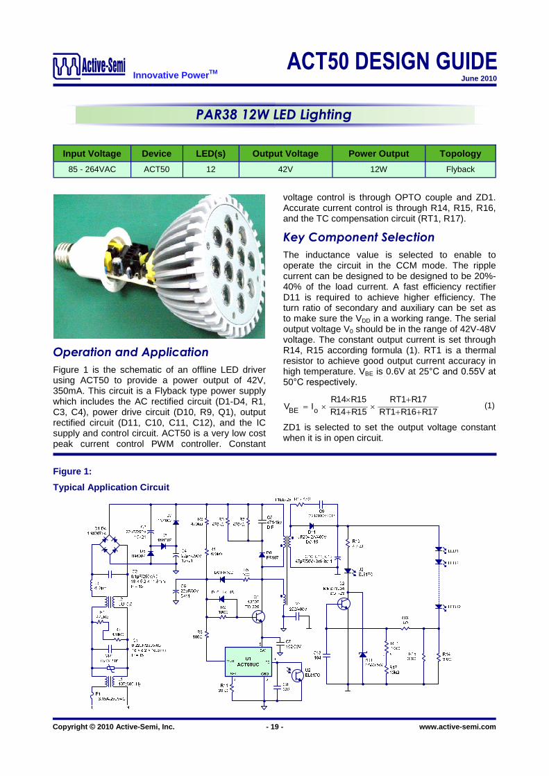
Operation and Application
Figure 1 is the schematic of an offline LED driver using ACT50 to provide a power output of 42V, 350mA. This circuit is a Flyback type power supply which includes the AC rectified circuit (D1-D4, R1, C3, C4), power drive circuit (D10, R9, Q1), output rectified circuit (D11, C10, C11, C12), and the IC supply and control circuit. ACT50 is a very low cost peak current control PWM controller. Constant
voltage control is through OPTO couple and ZD1. Accurate current control is through R14, R15, R16, and the TC compensation circuit (RT1, R17).
Key Component Selection
The inductance value is selected to enable to operate the circuit in the CCM mode. The ripple current can be designed to be designed to be 20%-40% of the load current. A fast efficiency rectifier D11 is required to achieve higher efficiency. The turn ratio of secondary and auxiliary can be set as to make sure the VDD in a working range. The serial output voltage V0 should be in the range of 42V-48V voltage. The constant output current is set through R14, R15 according formula (1). RT1 is a thermal resistor to achieve good output current accuracy in high temperature. VBE is 0.6V at 25°C and 0.55V at
50°C respectively.
ZD1 is selected to set the output voltage constant when it is in open circuit.

ACT50 DESIGN GUIDE Innovative PowerTM June 2010
Copyright © 2010 Active-Semi, Inc. - 20 - www.active-semi.com
Bill of Materials PCB Layout
Efficiency vs. Input Voltage
90
88
86
84
82
80
AC
T50-001
Effi
cien
cy (
%)
Transformer Specification
Electrical Specifications
12 LEDs
Input Voltage (V)
85 125 165 205 245 265
78mm
34mm
Output Current vs. Input Voltage 352
340
328
316
304
292
280
AC
T50-002
Out
put C
urre
nt (
mA
)
12 LEDs
Input Voltage (V)
85 125 165 205 245 265
REF. DESCRIPTION MFTR.
U1 IC, ACT50 Active-Semi
U2 IC, EL817C, DIP-4 Everlight C1 Cap-X2 0.22ìF/250V,18x8.2x16.5mm, P=15mm UTX C2 Cap-X2 0.1ìF/250V,18x5.2x11.8mm, P=15mm UTX
C3-C4 Capacitor, Electrolytic, 22ìF/400V, 10×21mm KSC C5 Capacitor, Ceramic, 470pF/1kV, DIP POE C6 Capacitor, Electrolytic, 22ìF/35V, 5×11mm KSC C7 Capacitor, Ceramic, 1000pF/50V, 0805 POE C8 Capacitor, Ceramic, 3300pF/25V, 0805 POE C9 Capacitor, Ceramic, 220pF/1kV, DIP POE
C10-C12 Capacitor, Electrolytic, 47ìF/50V, 6.3×11mm KSC C13 Capacitor, Ceramic, 0.1ìF/25V, 0805 POE Y1 Y1 Capacitor, 2200pF/400VAC, DIP POE
D1-D7 Rectifier, 1000V/1A, 1N4007 DO-41 Good-Ark D8 Diode, Ultra Fast, FR107, 1000V/1A DO-41 Good-Ark D9 Diode, Ultra Fast, FR102, 100V/1A DO-41 Good-Ark
D10 Diode, Switching, 75V/150mA, LL4148 Good-Ark D11 Diode, Ultra Fast, UF204, 400V/2.0A, DO-15 Good-Ark ZD1 Diode, Zener, GMZJ47A, 47V, 0.5W, MICRO-MELF PANJIT Q1 Transistor, NPN, D13007, TO-220 Huawei Q2 Amplifier Transistor, NPN, MMBT3904, SOT-23
F1 Fuse: 3.15A 250V 3.6×10mm With Pigtail, Ceramic tube. Walter
L1 Inductor, T9×5×3C, R12kÙ 13T 800µH L2 Inductor, LP = 28~40mH, Bobbin UU10.5 L3 Axial Inductor, 820µH, 0410, DIP
R1, R4, R6, R7 Chip Resistor, 470kÙ, 1206, 5% TY-OHM
R5 Chip Resistor, 10Ù, 1206, 5% TY-OHM R8 Chip Resistor, 100Ù, 1206, 5% TY-OHM R9 Chip Resistor, 47Ù, 1206, 5% TY-OHM
R11 Chip Resistor, 39kÙ, 0805, 5% TY-OHM R12 Chip Resistor, 47Ù, 1206, 5% TY-OHM R13 Chip Resistor, 4.7kÙ, 0603, 5% TY-OHM
R14, R15 Chip Film Resistor, 3.6Ù, 1206, 1% TY-OHM R16 Chip Resistor, 1kÙ, 0603, 5% TY-OHM R17 Chip Resistor, 10kÙ, 0603, 5% TY-OHM
T1 Transformer EE-25, BobbinTF-2202 10Pin Vertical, LP = 1.2mH
RT1 NTC minus Thermistor Compensation 10kÙ, ¢5mm, 5% TY-OHM
VR1 Varistor, TVR07431KSY, ¢7, 430V, ±10%, DIP Thinking H/S Heat Sunk: JD-YI Series L=20mm, Black JIEDA
For Q1 Silicon Insulation: TO-220 For Q1 Insulation Washer: Ö3mm For Q1 Pan Head Screw+Spring washer Ö3×8mm For Q1 Nut Ö3
WINDING TERMINAL
TURNS WIRE INSULATION
START FINISH TYPE SIZE × QTY LAYER THICK/WIDE LAYER
P1 3 1 83 2UEW 0.25Ö×1 2 25µ/8.5mm 2
SH1 5 Open 40 2UEW 0.15Ö×2 1 25µ/8.5mm 2
S1 10 P 41 TEXE 0.2Ö×2 1 25µ/8.5mm 2
SH2 5 Open 0.9 Copper 7mm 1 25µ/8.5mm 2
P2 4 5 12 2UEW 0.3Ö×1 1 25µ/8.5mm 2
SH3 5 Open 1.1 Copper 7mm (Core Outer)
1 25µ/8.5mm 2
Build Up
EVALUATION KITS VIN I0 LED(s) ACT50UC-T-LED06 85-264VAC 280-350mA 12
ITEM DESCRIPTION CONDITION LIMITS
1 Electrical Strength 50Hz, 1 minute, from Primary and Secondary 3kVAC
2 P1 Inductance Inductance between pin 1 and pin 3 at 1VAC & 1kHz
1.2mH ±7%
3 P1 Leakage Inductance
Inductance between pin 1 and pin 3 with pins 5-4 and 10-P shorted
75µH
P1 and P2 are Primary, P1 is Secondary (Bobbin: EE-25 Horizontal)
P1
P2
4
5
SH1
3
1
SH2
S1
10
PSH3 Pin3
PinP
Pin1SH1
S1Open
Pin5
P1
P2
Pin10
Pin5
Pin5
Pin4
Pin5
SH2 SH3

ACT50 DESIGN GUIDE Innovative PowerTM June 2010
Copyright © 2010 Active-Semi, Inc. - 21 - www.active-semi.com
FEATURES Universal AC Input
High Efficiency
Constant Voltage Control & Short Circuit Protection
CC Temperature Compensation
±5% Current Accuracy
Exceed Energy Start 2.0 Regulation
Small SOT23-5 Package
APPLICATIONS
Off-Line Isolated LED Driver
Operation and Application
Figure 1 is the schematic of an offline LED driver using ACT50 to provide a power output of 35V, 350mA. This circuit is a flyback type power supply which includes the AC rectified circuit (D1-D4, L1, R1, C1, C2), power drive circuit (D9, R6, Q1), output rectified circuit (D10, C8, C9) and the IC supply and control circuit. ACT50 is a very low cost
peak current control PWM controller. Constant voltage control is through OPTO coupler and ZD1. Accurate current control is through R10 and the TC compensation circuit (R9, R13, R14).
Key Component Selection
The inductance value is selected to enable to operate the circuit in the CCM mode. The ripple current can be designed to be 20%-40% of the load current. A fast efficiency rectifier D10 is required to achieve higher efficiency. The turn ratio of secondary and auxiliary can be set as 2.8 to make sure the VDD in a working range. The serial output voltage V0 should be in the range of 35V-40V voltage. The constant output current is set through R10 according formula (1). R14 is a thermal resistor to achieve good output current accuracy in high temperature. VBE is 0.6V at 25C and 0.55V at 50C respectively.
ZD1 is selected to set the output voltage constant when it is in open circuit.
Figure 1:
Typical Application Circuit
35V, 12W, 350mA High Efficiency Solutions
Input Voltage LED(s) Output Voltage Power Output Topology
85 - 264VAC 10 35V 12W Flyback
Device
ACT50
9R13R)T(14R13R)T(14R
10RIV 0BE
(1)

ACT50 DESIGN GUIDE Innovative PowerTM June 2010
Copyright © 2010 Active-Semi, Inc. - 22 - www.active-semi.com
Bill of Materials PCB Top and Bottom Layers
EVALUATION KITS VIN I0 LED(s) ACT50UC-T-LED07 85-264VAC 280-350mA 9 or 10
Build Up
REF. DESCRIPTION MFTR.
IC1 IC, ACT50UC-T, SOT23-5 Active-Semi
IC2 IC, EL817C, DIP-4 Everlight
C1, C2 Capacitor, Electrolytic, 10µF/400V, 8×12mm KSC
C3 Capacitor, Ceramic, 1000pF/1kV POE
C4 Capacitor, Electrolytic, 22µF/50V, 5×11mm KSC
C5 Capacitor, Ceramic, 1000pF/50V, 0805, SMD POE
C6, C10 Capacitor, Ceramic, 3300pF/50V, 0805, SMD POE
C7 Capacitor, Ceramic, 220pF/50V, 1206, SMD POE
C8, C9 Capacitor, Electrolytic, 100µF/50V, 8×12mm KSC
D1-D4 Diode, Ultra Fast, 1000V/1A 1N4007 DO-41 Good-Ark
D5 Diode, Ultra Fast, FR107, 1000V/1.0A, DO-41 Good-Ark
D6 Diode, Switching, 75V/150mA LL4148 MINI-MELF Good-Ark
D9 Diode, Switching, 75V/150mA 1N4148, DO-15 Good-Ark
D10 Diode, Super Fast, SF54, 300V/3.0A, DO-201AD Good-Ark
ZD1 Diode, Zener, GLZJ36A, 36V, 0.5W, MINI-MELF Good-Ark
L1 Axial Inductor, 330µH, 0410, DIP Amode Tech
Q1 Transistor, NPN, 600V, 1.5A, D13003X, TO-26 Hua Wei
Q2 Transistor, NPN, KTC9014, TO-92 KEC
F1 Fuse: 1A 250V 3.6×10mm With Pigtail Walter
R1 Chip Resistor, 3kÙ, 0805, 5% TY-OHM
R2 Chip Resistor, 750kÙ, 1206, 5% TY-OHM
R3 Chip Resistor, 500kÙ, 0805, 5% TY-OHM
R4 Chip Resistor, 100kÙ, 1206, 5% TY-OHM
R5 Chip Resistor, 100Ù, 0805, 5% TY-OHM
R6 Chip Resistor, 200Ù, 0805, 5% TY-OHM
R7 Chip Resistor, 39kÙ, 0805, 1% TY-OHM
R8 Chip Resistor, 2kÙ, 0805, 5% TY-OHM
R9 Chip Resistor, 1kÙ, 0805, 5% TY-OHM
R10 Meter Film Resistor, 1.87Ù, 1/2W DIP, 1% TY-OHM
R11 Chip Resistor, 47Ù, 1206, 5% TY-OHM
R12 Chip Resistor, 100Ù, 1206, 5% TY-OHM
R13 Chip Resistor, 820Ù, 0603, 5% TY-OHM
R14 NTC Minus Thermistor Compensation 10kÙ, 5% Thinking
VR1 Varistor, TVR05471KSY, ¢5, 470V, ±10% Thinking
YC1 Y1 Capacitor, 1000pF/400V, DIP UTX
T1 Transformer, LP = 1.8mH, EE19
WINDING
TERMINAL
TURNS
WIRE INSULATION
START FINISH TYPE SIZE × QTY LAYER THICK/WIDE LAYER
SH1 1 Open 30 2UEW 0.15Ö×2 1 25µ/8.5mm 2
P1 2 1 110 2UEW 0.25Ö×1 2 25µ/8.5mm 2
SH2 3 Open 30 2UEW 0.15Ö×2 1 25µ/8.5mm 2
S1 8 5 40 TEXE 0.45Ö×1 1 25µ/8.5mm 2
SH3 3 Open 1.1 Copper 7mm 1 25µ/8.5mm 3
P2 4 3 18 2UEW 0.15Ö×1 1 25µ/8.5mm 3
ITEM DESCRIPTION CONDITION LIMITS
1 Electrical Strength 50Hz, 1 minute, from Primary and Secondary 3kVAC
2 P1 Inductance Inductance between pin 1 and pin 2 at 1VAC & 1kHz
1.8mH ±7%
3 P1 Leakage Inductance
Inductance between pin 1 and pin 2 with pins 3-4 and 5-8 shorted
75µH
Transformer Specification
Electrical Specifications
P1 and P2 are Primary, S1 is Secondary (Bobbin: EE-19 Horizontal)
Efficiency vs. Input Voltage 90
86
82
78
74
70
AC
T50-001
Output Current vs. Input Voltage 400
360
320
280
240
200
AC
T50-002
Out
put C
urre
nt L
oad
(mA
)
10 LEDs
10 LEDs
Input Voltage (V)
85 125 165 205 245 265
Input Voltage (V)
85 125 165 205 245 265
Effi
cien
cy (
%)
Typical Performance Characteristics
36m
m
47mm
8
S1
5
P1
1
2
P2
3
4
SH1
SH2
SH
3
Open
Open
Pin1
Pin8
SH1
Pin5
Pin4
Pin2
Pin1Pin3
Pin3
P1
SH2
S1
P2
SH3
Pin3 Open

ACT50 DESIGN GUIDE Innovative PowerTM June 2010
Copyright © 2010 Active-Semi, Inc. - 23 - www.active-semi.com
Input Voltage LED(s) Output Voltage Power Output Topology
85 - 264VAC 7LED or 300mA or 600mA or 900mA 28V 21W Buck
Device
ACT50
FEATURES Universal AC input
High Efficiency
Constant Voltage Control & Short Circuit Protection
CC Temperature Compensation
±5% Current Accuracy
Exceed Energy Start 2.0 Regulation
Small DIP-8 Package
APPLICATIONS
Off-Line Isolated LED Driver
Operation and Application
Figure 1 is the schematic of an offline LED driver using ACT50 to provide a power output of 28V, 350mA. This circuit is a buck type power supply which includes the AC rectified circuit (D1-D7, L1-L3, C1-C5), power drive circuit (D10, R11, Q1), output rectified circuit (D11, C11, C12) and the IC supply and control circuit. ACT50 is a very low cost peak current control PWM controller. Constant
voltage control is through OPTO couple and D12. Accurate current control is through R13 and LM358 control circuit.
Key Component Selection
The inductance value is selected to enable to operate the circuit in the CCM mode. The ripple current can be designed to be 20%-40% of the load current. A fast efficiency rectifier D11 is required to achieve higher efficiency. The turn ratio of secondary and auxiliary can be set as to make sure the VDD in a working range. The serial output voltage V0 should be in the range of 28V-32V voltage. The constant output current is set through R13 according formula (1, 2, 3).
D12 is selected to set the output voltage constant when it is in open circuit.
Figure 1:
Typical Application Circuit
28V, 21W, 350mA High Efficiency Solutions
';
'8)
'8)/+
'8)
13R17R)21R20R//()19R18R(
5.2I01
(1)
13R17R)23R22R//()19R18R(
5.2I02
(2)
13R17R)25R24R//()19R18R(
5.2I03
(3)

ACT50 DESIGN GUIDE Innovative PowerTM June 2010
Copyright © 2010 Active-Semi, Inc. - 24 - www.active-semi.com
280
19.5
mm
50.3mm
Bill of Materials PCB Top and Bottom Layers
EVALUATION KITS VIN I0 LED(s)
ACT50DH-LED08 85-264VAC
I01 350mA±5%
I02 600mA±5%
I03 900mA±5%
7×300mA, or 7×600mA, or 7×900mA
Build up
WINDING
TERMINAL
TURNS
WIRE INSULATION
START FINISH TYPE SIZE × QTY LAYER THICK/WIDE LAYER
P1 3 1 87 2UEW 0.25Ö×1 1 25µ/8.5mm 2
SH1 1 Open 30 2UEW 0.15Ö×2 1 25µ/8.5mm 2
S1 10 11 28 TEXE 0.6Ö×1 1 25µ/8.5mm 2
SH2 6 Open 1.1 Copper 7mm 1 25µ/8.5mm 2
P2 5 6 14 2UEW 0.25Ö×1 1 25µ/8.5mm 2
ITEM DESCRIPTION CONDITION LIMITS
1 Electrical Strength 50Hz, 1 minute, from Primary and Secondary 3kVAC
2 P1 Inductance Inductance between pin 1 and pin 3 at 1VAC & 1kHz
0.8mH ±7%
3 P1 Leakage Inductance
Inductance between pin 1 and pin 3 with pins 5-6 and 10-11 shorted
75µH
Efficiency vs. Input Voltage
Input Voltage (V)
110 130 150 170 190 210 230
AC
T50-001
Effi
cien
cy (
%)
Output Current vs. Input Voltage 940
820
700
580
460
340
AC
T50-002
Out
put C
urre
nt L
oad
(mA
)
Transformer Specification
Electrical Specifications
REF. DESCRIPTION MFTR. U1 IC, ACT50UC-T, DIP-8 Active U2 IC, EL817C, DIP-4 Everlight U3 IC, LM358, DIP-8 Everlight U4 IC, TL431, TO-92 USE
C1-C3 Capacitor-X2 0.1µF275V 18×6×12×15mm UTX
C4, C5 Capacitor, Electrolytic, 22µF/250V,
10×20mm KSC
C6 Capacitor, Ceramic, 2200pF/1kV, DIP POE C8 Capacitor, Electrolytic, 22µF/35V, 5×11mm KSC C10 Capacitor, Ceramic, 0.1µF/25V POE
C11, C12 Capacitor, Electrolytic, 220pF/35V, 8×12mm KSC C13 Mul-Cap Ceramic, 0.1µF/25V, DIP POE C15 Mul-Cap Ceramic, 0.01µF/25V, DIP POE C16 Safety Capacitor, Y2, 2200pF/400V, P = 10mm, DIP UTX
D1-D8 Diode, Ultra Fast, UF4007, 1000V/1.0A, DO-41 Good-Ark D9 Diode, Ultra Fast, UF102, 200V/1.0A, DO-41 PANJIT
D10, D13 Diode, Switching, 75V/150mA, LL4148 MINI-MELF Good-Ark D11 Diode, Schottky, HER204, 300V/2A, DO-15 ST D12 Diode, Zener, GDZJ27D, 27V, 0.5W, DO-35 PANJIT L1 Inductor, UU10.5, 28mH
L2, L3 Axial Inductor, 220µH, 0410, DIP Amode Tech
Q1 Transistor, NPN, 600V, 1.5A, D13003X, TO-220 Hua Wei F1 Fuse: 2A 250V 3.6×10mm with Pigtail Walter R4 Meter Film Resistor, 27kÙ, 1/4W, 1% TY-OHM
R5, R6 Carbon Film Resistor, 750kÙ, 1/4W, 5% TY-OHM R7 Carbon Film Resistor, 10Ù, 1/4W, 5% TY-OHM R8 Carbon Film Resistor, 100kÙ, 1W, 5% TY-OHM R10 Carbon Film Resistor, 10Ù, 1/2W, 5% TY-OHM
R11, 15 Carbon Film Resistor, 150Ù, 1/4W, 5% TY-OHM R12 Carbon Film Resistor, 8.6kÙ, 1/4W, 5% TY-OHM R13 Meter Film Resistor, 0.1Ù, 1/4W, 1% TY-OHM R14 Carbon Film Resistor, 6.2kÙ, 1/4W, 5% TY-OHM R16 Carbon Film Resistor, 33kÙ, 1/4W, 5% TY-OHM R17 Carbon Film Resistor, 15kÙ, 1/4W, 5% TY-OHM R18 Carbon Film Resistor, 69Ù, 1/4W, 5% TY-OHM R19 Carbon Film Resistor, 560Ù, 1/4W,5% TY-OHM R20 Carbon Film Resistor, 270Ù, 1/4W, 5% TY-OHM R21 Carbon Film Resistor, 0Ù, 1/4W, 5% TY-OHM R22 Carbon Film Resistor, 180Ù, 1/4W, 5% TY-OHM R23 Carbon Film Resistor, 820Ù, 1/4W,5% TY-OHM R24 Carbon Film Resistor, 240Ù, 1/4W, 5% TY-OHM R25 Carbon Film Resistor, 5.1kÙ, 1/4W, 5% TY-OHM VR1 TVR07391KSY ¢7, 390V ±10% Thinking T1 Transformer, LP = 0.8mH, EPC25 TY-OHM
4 LEDs
8 LEDs
84
76
72
68
64
60
80
86
Input Voltage (V)
85 125 165 205 245 265
I01
I02
I03
P1 and P2 are Primary, S1 is Secondary (Bobbin: EPC25 Horizontal)
I01
I03
I02
Typical Performance Characteristics
openPin10Pin11
Pin6
Pin3
Pin1
Pin1
Pin5
P1
S1
P2
SH2
SH1
Pin6
open
S1
11
10
P1
1
3
P2
6
5
SH1
SH
2