Embed Size (px)
Citation preview

Application ReportSCAA059C–March 2003–Revised October 2007
AC-Coupling Between Differential LVPECL, LVDS, HSTL,and CML
Kal Mustafa/Chris Sterzik................................................................................. High Performance Analog
ABSTRACTThis report provides a quick reference of ac-coupling techniques for interfacingbetween different logic levels. The four differential signaling levels found in this reportare low-voltage positive-referenced emitter coupled logic (LVPECL), low-voltagedifferential signals (LVDS), high-speed transceiver logic (HSTL), and current-modelogic (CML). From these four differential signaling levels, 16 interface cases areprovided.
Contents1 AC-Coupling......................................................................................... 22 References......................................................................................... 16
List of Figures
1 AC-Coupling to Shift Common-Mode Voltage .................................................. 22 Input and Output Parameters ..................................................................... 23 LVPECL to LVPECL................................................................................ 34 LVPECL to LVPECL................................................................................ 45 LVPECL to LVDS................................................................................... 46 LVPECL to CML ................................................................................... 57 LVPECL to CML Converter........................................................................ 58 LVPECL to HSTL ................................................................................... 69 LVDS to LVPECL................................................................................... 610 LVDS to LVPECL................................................................................... 711 LVDS to LVDS ...................................................................................... 712 LVDS to LVDS ...................................................................................... 813 LVDS to CML ....................................................................................... 814 LVDS to CML Translator........................................................................... 915 LVDS to HSTL ...................................................................................... 916 CML to LVPECL .................................................................................. 1017 CML to LVPECL .................................................................................. 1018 CML to LVDS ...................................................................................... 1119 CML to LVDS ...................................................................................... 1120 CML to CML ....................................................................................... 1221 CML to HSTL ...................................................................................... 1222 CML to HSTL ...................................................................................... 1323 HSTL to LVPECL ................................................................................. 1324 HSTL to LVPECL Converter..................................................................... 1325 HSTL to LVDS..................................................................................... 1426 HSTL to LVDS..................................................................................... 1427 HSTL to LVDS Converter ........................................................................ 1428 HSTL to CML ...................................................................................... 1529 HSTL to HSTL ..................................................................................... 1530 HSTL to LVPECL to HSTL Using the CDCLVP110 .......................................... 16
SCAA059C–March 2003–Revised October 2007 AC-Coupling Between Differential LVPECL, LVDS, HSTL, and CML 1Submit Documentation Feedback

www.ti.com
1 AC-Coupling
Vterm
VOH = 1.4 V
VOL= 1 V
VOH = Vterm + 0.2 V
VOL = Vterm - 0.2 V
Receiver
VIH (MAX)
VIH (MIN)
VIL (MAX)
VIL (MIN)
Driver
VOH (MAX)
VOH(MIN)
IOH (MAX)
VOL (MAX)
VOL (MIN)
I/O Parameters
VCM
AC-Coupling
List of Tables
1 Typical LVPECL, LVDS, HSTL, and CML Outputs ............................................ 32 Typical LVPECL, LVDS, CML, and HSTL Input Levels ....................................... 33 Interface Table ...................................................................................... 3
AC-coupling is used to change the common-mode voltage level when interconnecting different physicallayers. A simple example is shown in Figure 1.
Figure 1. AC-Coupling to Shift Common-Mode Voltage
The capacitor in Figure 1 removes the dc component of the signal (common-mode voltage), while the accomponent (voltage swing) is passed on. The resistor to Vterm in Figure 1 represents the biasing structureused to set the common-mode voltage on the receiver side of the ac-coupling capacitor. Throughout thisdocument the capacitor value is 10nF and the biasing structure is either part of the internal biasing of thereceiver or an external resistor pull-up and/or pull-down network.
In high-speed applications, ac-coupling is only recommended for dc-balanced signals. AC couplinggenerates base-line wander in high-speed serial data transmission which is non-dc balanced. Examples ofdc-balanced signals are 50% duty cycle clocks, Manchester-coded data, and ANSI fiber channel 8B/10Bencoded data.
The more common physical layers (PHYs) that appear in the telecom industry are LVDS, LVPECL, HSTL,and CML. In order to interface these different PHYs, it is important to understand the input and outputlevels of each. The output and input levels for each of the PHYs are found in Table 1 and Table 2respectively, and the output and input levels are illustrated in Figure 2.
Figure 2. Input and Output Parameters
2 AC-Coupling Between Differential LVPECL, LVDS, HSTL, and CML SCAA059C–March 2003–Revised October 2007Submit Documentation Feedback
www.ti.com
1.1 LVPECL
e.g.
CDC111
CDCVF111
CDCLVP110
SN65LVDS101
150 W
150 W
LVPECL
Driver
LVPECL
Receiver
130 W
Z0= 50 W
VCC
VCC
83 W
83 W
130 W
Z0= 50 W
AC-Coupling
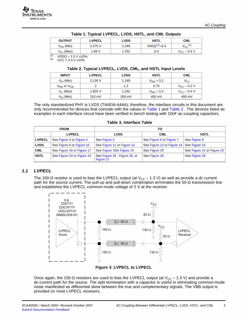
Table 1. Typical LVPECL, LVDS, HSTL, and CML OutputsOUTPUT LVPECL LVDS HSTL CMLVOH (Min) 2.275 V 1.249 VDDQ (1)–0.4 VCC
(2)
VOL (Max) 1.68 V 1.252 0.4 VCC – 0.4 V(1) VDDQ = 1.5 V ±10%.(2) VCC = 3.3 V ±10%
Table 2. Typical LVPECL, LVDS, CML, and HSTL Input LevelsINPUT LVPECL LVDS HSTL CML
VIH (Min) 2.135 V 1.249 VRef + 0.2 VCC
VRef or VCM 2 1.2 0.75 VCC – 0.2 VVIL (Max) 1.825 V 1.252 VRef – 0.2 VCC – 0.4 VVID (Min) 310 mV 200 mV 400 mV 400 mV
The only standardized PHY is LVDS (TIA/EIA-644A); therefore, the interface circuits in this document areonly recommended for devices that coincide with the values in Table 1 and Table 2 . The devices listed asexamples in each interface circuit have been verified in bench testing with 10nF ac-coupling capacitors.
Table 3. Interface TableFROM TO
LVPECL LVDS CML HSTLLVPECL See Figure 3 or Figure 4 See Figure 5 See Figure 6 or Figure 7 See Figure 8LVDS See Figure 9 or Figure 10 See Figure 11 or Figure 12 See Figure 13 or Figure 14 See Figure 15CML See Figure 16 or Figure 17 See Figure 18or Figure 19 See Figure 20 See Figure 21 or Figure 22HSTL See Figure 23 or Figure 24 See Figure 25 , Figure 26, or See Figure 28 See Figure 29
Figure 27
The 150-Ω resistor is used to bias the LVPECL output (at VCC – 1.3 V) as well as provide a dc currentpath for the source current. The pull-up and pull-down combination terminates the 50-Ω transmission lineand establishes the LVPECL common-mode voltage of 2 V at the receiver.
Figure 3. LVPECL to LVPECL
Once again, the 150-Ω resistors are used to bias the LVPECL output (at VCC – 1.3 V) and provide adc-current path for the source. The split termination with a capacitor is useful in eliminating common-modenoise manifested as differential skew between the true and complementary signals. The VBB output isprovided on most LVPECL receivers.
SCAA059C–March 2003–Revised October 2007 AC-Coupling Between Differential LVPECL, LVDS, HSTL, and CML 3Submit Documentation Feedback

www.ti.com
LVPECL ReceiverLVPECL DriverVBB
!
Z = 50o W
Z = 50o W
150 W
150 W
50 W
50 W
e.g.CDC111
CDCVF111CDCLVP110
SN65LVDS101
e.g.
CDC111
CDCVF111
CDCLVP110
SN65LVDS101
150 WLVPECL
Driver
LVDS
Receiver100 W
10 KW
e.g.
CDCLVD110
SN65LVDS100
SN65LVDS104
Z0= 50 W
3.3 V
Z0= 50 W
150 W 10 KW
AC-Coupling
Figure 4. LVPECL to LVPECL
The 150-Ω resistor is used to dc-bias the LVPECL output (at VCC – 1.3 V) as well as provide a dc currentpath for the source current. The external 100Ω is used to terminate the differential 100-Ω transmission lineimpedance as well as provide sufficient signal swing to drive the wide common-mode LVDS receivers.The two 10kΩ resistors set the receiver common-mode voltage to 1.65V, which is within thecommon-mode voltage range of an LVDS receiver (see TIA/EIA-644). For LVDS receivers with integrated100-. termination the external 100-Ω resistor in Figure 5 is not required (e.g., SN65LVDT33,SN65LVDT100, and SN65LVDT122).
Figure 5. LVPECL to LVDS
In Figure 6, there are two resistors, the 150Ω (R-bias) and Ra. The 150-Ω resistor is required to dc-biasthe LVPECL outputs prior to ac-coupling. The value of R-bias ranges from 140Ω to 240Ω. In the casewhere the differential LVPECL output is larger than what the CML receiver can tolerate, then Ra should beused to attenuate the LVPECL output such that it meets the input voltage required for the CML receiver.
4 AC-Coupling Between Differential LVPECL, LVDS, HSTL, and CML SCAA059C–March 2003–Revised October 2007Submit Documentation Feedback

www.ti.com
e.g.
CDC111
CDCVF111
CDCLVP110
SN65LVDS101
150 WLVPECL
Driver
CML
Receiver
Z0 = 50 W
50 W
VCC
OptionalRa = 25 W
OptionalRa = 25 W
Z0 = 50 W
150 W
50 W
SN65CML100SN65CML100
A
B
LVPECL
Input
CML
Output
Y
Z
3.3 V
3.3 V
50 W
50 W
AC-Coupling
Figure 6. LVPECL to CML
For example, if the LVPECL output swing is 750 mV and the required CML receiver input is 400 mV, thenthe attenuation factor is 0.68, which requires Ra ≅ 23Ω. In Figure 6 the CML receiver is assumed to beself-biased.
The SN65CML100 in Figure 7 can be used as an LVPECL to CML converter. The 50-Ω pull-up resistorsare required to bias the SN65CML100 outputs. The coupling capacitors on the inputs (optional, but shownfor completeness) are used assuming that the LVPECL source is properly terminated.
Figure 7. LVPECL to CML Converter
The 150-Ω resistor is used to bias the LVPECL output (at VCC–1.3 V) as well as provide a dc current pathfor the source. The equivalent 50-Ω. Thevenin resistors of R1 and R2 are used to terminate the traceimpedance as well as to set the common-mode voltage (VCM = 0.75 V) for the HSTL receiver, Figure 8.
SCAA059C–March 2003–Revised October 2007 AC-Coupling Between Differential LVPECL, LVDS, HSTL, and CML 5Submit Documentation Feedback

www.ti.com
R1
R2
R1
R2
e.g.,CDC111
CDCVF111CDCLVP110
SN65LVDS101
HSTLReceiver
LVPECLDriver
VCC
VCC
150 W
150 W
Z = 50O
W
Z = 50O
W
Note:
For V = 3.3 V, use R1 = 220 , R2 = 68CC W W
For V = 2.5 V, use R1 = 167 , R2 = 71
For V = 1.5 V, use R1 = R2 = 100
CC
CC
W W
W
1.2 LVDS
e.g.,CDCLVD110
SN65LVDS100SN65LVDS122SN65LVDS31
LVDS Driver LVPECLReceiver
VCC
VCC
83 W
130 W
83 W
130 W
Z = 50O
W
Z = 50O
W
AC-Coupling
Figure 8. LVPECL to HSTL
The Thevenin equivalent of the 83Ω and 130Ω in Figure 9, matches the 50-Ω transmission line impedanceas well as sets the common-mode voltage (VCM = 2 V) for the LVPECL receiver.
Figure 9. LVDS to LVPECL
Figure 10 is recommended when VBB is available on the LVPECL receiver. The split termination with thecapacitor to ground is useful in eliminating common-mode noise manifested as differential skew betweenthe true and complementary signals.
6 AC-Coupling Between Differential LVPECL, LVDS, HSTL, and CML SCAA059C–March 2003–Revised October 2007Submit Documentation Feedback

www.ti.com
e.g.,CDCLVD110
SN65LVDS100SN65LVDS122SN65LVDS31
LVDS DriverLVPECL
Receiver
VBB
Z = 50O
W
Z = 50O
W
50 W
50 W
e.g.
CDCLVD 110
SN 65 LVDS 100
SN 65 LVDS 122
SN 65 LVDS 104
LVDS
Driver
LVDS
Receiver100 W
Z = 50O
W
Z = 50O
W
3.3 V
10 kW
10 kW
AC-Coupling
Figure 10. LVDS to LVPECL
In Figure 11 is a combination of the more common 100-Ω termination and ac-coupling. It also assumesthat the LVDS receiver does not include on-chip termination.
Figure 11. LVDS to LVDS
Figure 12 has an advantage over Figure 11 of correcting for (differential) skew mismatch between the trueand complementary signals. Both Figure 11 and Figure 12 assume that the LVDS receiver is self-biased.
SCAA059C–March 2003–Revised October 2007 AC-Coupling Between Differential LVPECL, LVDS, HSTL, and CML 7Submit Documentation Feedback

www.ti.com
e.g.,CDCLVD110
SN65LVDS100SN65LVDS122SN65LVDS104
LVDS Driver LVDSReceiver
VBB
Z = 50O
W
Z = 50O
W
50 W
50 W
e.g.,SN65LVDS100CDCLVD110
SN65LVDS104
LVDS Driver CMLReceiver
Z = 50O
W
Z = 50O
W
VCC
10 kW
10 kW 10
0W
AC-Coupling
Figure 12. LVDS to LVDS
Most CML receivers have an on-chip termination, and there is no need for additional resistors to terminatethe transmission line. The two 10-kΩ resistors are only required if the CML receiver is not self-biased andmay vary form one vendor to another; see the manufacturer's data sheet for details.
Figure 13. LVDS to CML
The SN65CML100 has a wide-common mode receiver, which allows the device to be used as an LVDS toCML translator. Two 50-Ω pull-up resistors are required to terminate the trace and bias the SN65CML100output stage, as shown Figure 14. Figure 14 implies that the LVDS input is properly terminated.
8 AC-Coupling Between Differential LVPECL, LVDS, HSTL, and CML SCAA059C–March 2003–Revised October 2007Submit Documentation Feedback

www.ti.com
SN65CML100VBIAS
50 W
50 W
3.3 V
3.3 V
50 W
50 W
e.g.,CDCLVD110
SN65LVDS100SN65LVDS104
LVDSDriver HSTL Receiver
R1
R2
R1
R2
Z = 50O
W
Z = 50O
W
VCC
VCC
Note:
For V = 3.3 V, use R1 = 220 , R2 = 68CC W W
For V = 2.5 V, use R1 = 167 , R2 = 71
For V = 1.5 V, use R1 = R2 = 100
CC
CC
W W
W
AC-Coupling
Figure 14. LVDS to CML Translator
The value of the two resistors, R1 and R2 depends on the receiver supply voltage and the common-modevoltage range of the receiver. If the HSTL receiver has a 1.5-V supply, then R1 and R2 are 100Ω each(50Ω equivalent) to terminate the trace. For other supply voltages (see the note in Figure 15) R1 and R2should be chosen such that their parallel combination matches the transmission line and the mid-point isset to the common-mode of the HSTL receiver (VCM = 0.75 V).
Figure 15. LVDS to HSTL
SCAA059C–March 2003–Revised October 2007 AC-Coupling Between Differential LVPECL, LVDS, HSTL, and CML 9Submit Documentation Feedback

www.ti.com
1.3 CML
e.g.
SN 65 CML 100
CML
Driver
LVPECL
Receiver
e.g.
CDCLVP 110
CDCVF 111
CDC 111
Z = 50O
W
Z = 50O
W
3.3 V
3.3 V
50 W
50 W
e.g.,SN65LVDS101CDCLVP110CDCVF111
CDC111
e.g.,
SN65CML100
VBB
R1
R1
LVPECL
ReceiverCML Driver
3.3 V
3.3 V
50 W
50 W
Z = 50O
W
Z = 50O
W
AC-Coupling
The 50-Ω pull-up resistors are used to dc-bias the CML outputs and provide a source termination to matchthe transmission line. Figure 16 assumes that the LVPECL input stage is self-biased.
Figure 16. CML to LVPECL
The 50-Ω pull-up resistors are required for the SN65CML100 to bias and source-terminate thetransmission line. R1 in Figure 17 should be larger than 50Ω in case the CML output stage losses, inaddition to the PCB losses, are too high to meet the minimum differential input voltage (VID) swingrequirement of the LVPECL input stage.
Figure 17. CML to LVPECL
The 50-Ω pull-up resistors are used to dc-bias and source-terminate the SN65CML100 outputs. The LVDSreceiver has a wide input common-mode range (between 0 V and 2.4 V), that is, the receiver can acceptany signal within the common-mode range and a differential swing of at least 100 mV. Figure 18, assumesa self-biased LVDS receiver.
10 AC-Coupling Between Differential LVPECL, LVDS, HSTL, and CML SCAA059C–March 2003–Revised October 2007Submit Documentation Feedback

www.ti.com
e.g.
SN 65 CML100
CML
Driver
LVDS
Receiver
e.g.
SN 65 LVDS104
SN 65 LVDS33
CDCLVD 110
Z = 50O
W
Z = 50O
W
50 W
100 W
10 kW
3.3 V
50 W
3.3 V3.3 V
10 kW
e.g.,SN65LVDS100
CDCLVD110e.g.,
SN65CML100
VBB
R1
R1
LVDS ReceiverCML Driver
Z = 50O
W
50 W
Z = 50O
W
3.3 V
3.3 V
50 W
AC-Coupling
Figure 18. CML to LVDS
The 50-Ω pull-up resistors are required for the SN65CML100 to bias and source-terminate thetransmission line. R1 in Figure 19 should be larger than 50Ω in case the CML output stage losses, inaddition to the PCB losses, are too high to meet the minimum (voltage input differential (VID) swingrequirement of the LVDS input stage. Figure 19 assumes an internally generated bias voltage pin (VBB) isavailable.
Figure 19. CML to LVDS
CML comes in many distinctions; therefore, termination and bias structures are not applicable to all CMLdrivers and receivers. The 50-Ω pull-up resistors, in Figure 20, are required to dc-bias the SN65CML100and source-terminate the transmission line, while other CML drivers have integrated 50-Ω pull-upresistors, which do not require the external 50-Ω pull-up resistors.
The two 10-kΩ resistors are only required if the CML receiver is not self-biased and may vary from onevendor to another; see the manufacturer's data sheet for details.
SCAA059C–March 2003–Revised October 2007 AC-Coupling Between Differential LVPECL, LVDS, HSTL, and CML 11Submit Documentation Feedback

www.ti.com
e.g.,
SN65CML100
CML DriverCML
Receiver
Z = 50O
W
50 W
10 kW
3.3 V
Z = 50O
W
3.3 V
50 W
VCC
10
0W
10 kW
R1
R1
R2
R2
CML Driver HSTL Receiver
CLK0
CLK0
e.g.,
SN65CML100
e.g.,
CDCLVP110
Z = 50O
W
50 W
3.3 V
3.3 V
VCC
VCC
50 W
Note:
For V = 3.3 V, use R1 = 220 , R2 = 68CC W W
For V = 2.5 V, use R1 = 167 , R2 = 71
For V = 1.5 V, use R1 = R2 = 100
CC
CC
W W
W
Z = 50O
W
AC-Coupling
Figure 20. CML to CML
In Figure 21, the 50-Ω pull-up resistors are required to dc-bias the SN65CML100 outputs. The parallelcombination of R1 and R2 are used to set the HSTL common-mode voltage (VCM = 0.75 V).
Figure 21. CML to HSTL
The 50-Ω pull-up resistors are required to dc-bias the SN65CML100 outputs. The split termination with thecapacitor is useful in eliminating common-mode noise manifested as differential skew between the trueand complementary signals. VBB output may be provided by HSTL receiver. R1 in Figure 22 should belarger than 50Ω when the CML output stage and the PCB losses are too high to meet the minimumvoltage input differential (VID) swing requirement of the HSTL input stage.
12 AC-Coupling Between Differential LVPECL, LVDS, HSTL, and CML SCAA059C–March 2003–Revised October 2007Submit Documentation Feedback
www.ti.com
e.g.,
SN65CML100
CML Driver
R1
R1
VBB
e.g.,
CDCLVP110
HSTL Receiver
CLK0
CLK0
Z = 50O
W
3.3 V
Z = 50O
W
3.3 V
50 W
50 W
1.4 HSTL
e.g.,
CDCLVP110CDCVF111
CDC111
HSTL Driver LVPECL ReceiverVBB
Z = 50O
W
50 W
Z = 50O
W
50 W
SN65CML100CDCLVP110HSTLInput
LVPECLOutput
CLK1
CLK1
AC-Coupling
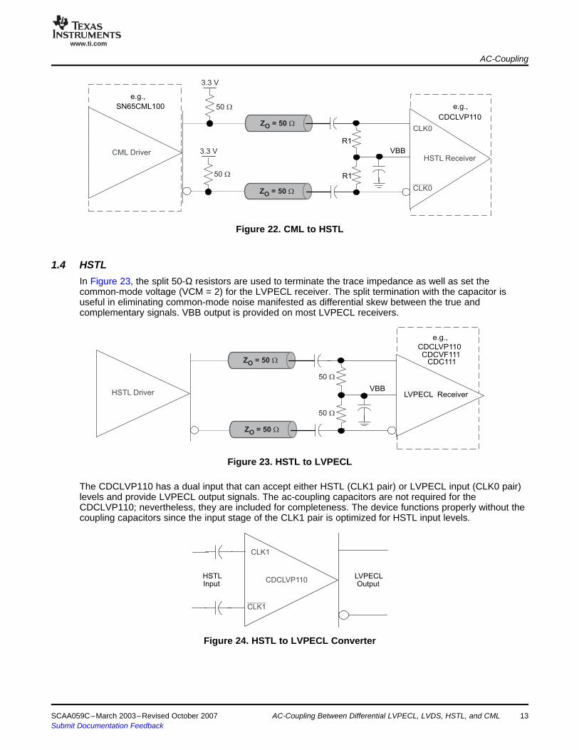
Figure 22. CML to HSTL
In Figure 23, the split 50-Ω resistors are used to terminate the trace impedance as well as set thecommon-mode voltage (VCM = 2) for the LVPECL receiver. The split termination with the capacitor isuseful in eliminating common-mode noise manifested as differential skew between the true andcomplementary signals. VBB output is provided on most LVPECL receivers.
Figure 23. HSTL to LVPECL
The CDCLVP110 has a dual input that can accept either HSTL (CLK1 pair) or LVPECL input (CLK0 pair)levels and provide LVPECL output signals. The ac-coupling capacitors are not required for theCDCLVP110; nevertheless, they are included for completeness. The device functions properly without thecoupling capacitors since the input stage of the CLK1 pair is optimized for HSTL input levels.
Figure 24. HSTL to LVPECL Converter
SCAA059C–March 2003–Revised October 2007 AC-Coupling Between Differential LVPECL, LVDS, HSTL, and CML 13Submit Documentation Feedback
www.ti.com
HSTL
Driver
LVDS
Receiver
e.g.
CDCLVD 110
SN 65 LVDS100
Z = 50O
W
100 W
10 kW
3.3 V
Z = 50O
W
10 kW
e.g.,CDCLVD110
SN65LVDS100
LVDS ReceiverVBB
HSTL Driver
Z = 50O
W
50 W
Z = 50O
W
50 W
CDCLVD110
SN65LVDS100HSTL
Input
50 W
VBIAS
3.3 V
3.3 V
50 W
50 W 50 W
AC-Coupling
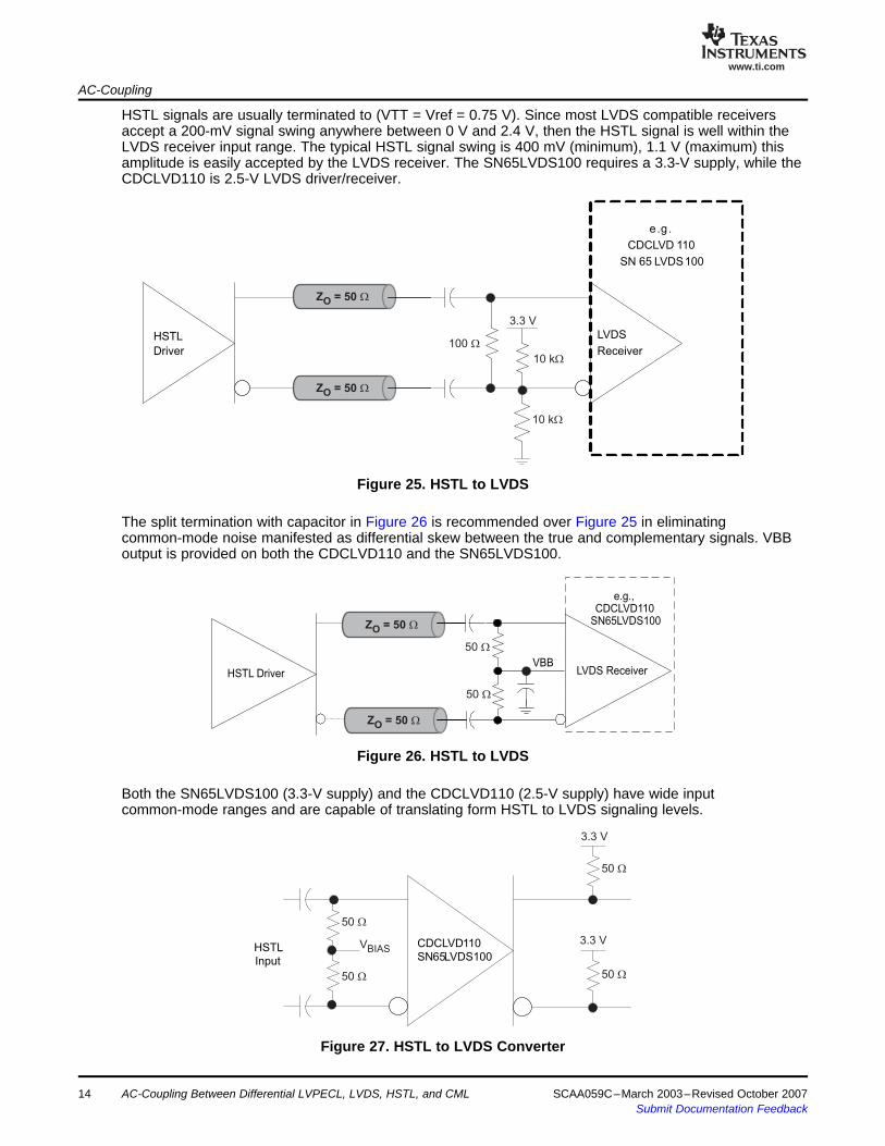
HSTL signals are usually terminated to (VTT = Vref = 0.75 V). Since most LVDS compatible receiversaccept a 200-mV signal swing anywhere between 0 V and 2.4 V, then the HSTL signal is well within theLVDS receiver input range. The typical HSTL signal swing is 400 mV (minimum), 1.1 V (maximum) thisamplitude is easily accepted by the LVDS receiver. The SN65LVDS100 requires a 3.3-V supply, while theCDCLVD110 is 2.5-V LVDS driver/receiver.
Figure 25. HSTL to LVDS
The split termination with capacitor in Figure 26 is recommended over Figure 25 in eliminatingcommon-mode noise manifested as differential skew between the true and complementary signals. VBBoutput is provided on both the CDCLVD110 and the SN65LVDS100.
Figure 26. HSTL to LVDS
Both the SN65LVDS100 (3.3-V supply) and the CDCLVD110 (2.5-V supply) have wide inputcommon-mode ranges and are capable of translating form HSTL to LVDS signaling levels.
Figure 27. HSTL to LVDS Converter
14 AC-Coupling Between Differential LVPECL, LVDS, HSTL, and CML SCAA059C–March 2003–Revised October 2007Submit Documentation Feedback
www.ti.com
e.g.,SN65CML100
CMLReceiver
HSTL Driver
10
0W
Z = 50O
W
Z = 50O
W
10 kW
10 kW
VCC
HSTL
Driver
HSTL
Receiver
50 W
VBIAS
Z = 50O
W
Z = 50O
W
50 W
AC-Coupling
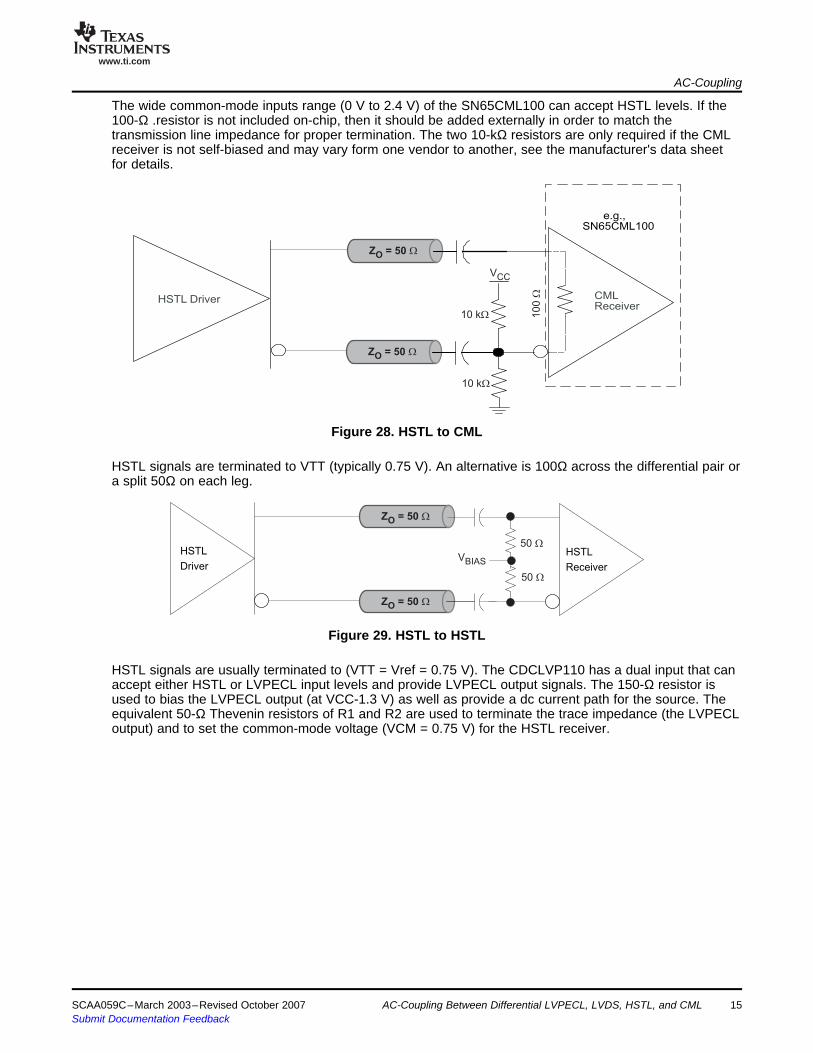
The wide common-mode inputs range (0 V to 2.4 V) of the SN65CML100 can accept HSTL levels. If the100-Ω .resistor is not included on-chip, then it should be added externally in order to match thetransmission line impedance for proper termination. The two 10-kΩ resistors are only required if the CMLreceiver is not self-biased and may vary form one vendor to another, see the manufacturer's data sheetfor details.
Figure 28. HSTL to CML
HSTL signals are terminated to VTT (typically 0.75 V). An alternative is 100Ω across the differential pair ora split 50Ω on each leg.
Figure 29. HSTL to HSTL
HSTL signals are usually terminated to (VTT = Vref = 0.75 V). The CDCLVP110 has a dual input that canaccept either HSTL or LVPECL input levels and provide LVPECL output signals. The 150-Ω resistor isused to bias the LVPECL output (at VCC-1.3 V) as well as provide a dc current path for the source. Theequivalent 50-Ω Thevenin resistors of R1 and R2 are used to terminate the trace impedance (the LVPECLoutput) and to set the common-mode voltage (VCM = 0.75 V) for the HSTL receiver.
SCAA059C–March 2003–Revised October 2007 AC-Coupling Between Differential LVPECL, LVDS, HSTL, and CML 15Submit Documentation Feedback

www.ti.com
HSTLReceiver
R1
R2
R1
R2
SN65CML100CDCLVP110HSTLInput
CLK1
CLK1
Z = 50O
W
150 W
150 W
VCC
VCC
Z = 50O
W
Note:
For V = 3.3 V, use R1 = 220 , R2 = 68CC W W
For V = 2.5 V, use R1 = 167 , R2 = 71
For V = 1.5 V, use R1 = R2 = 100
CC
CC
W W
W
2 References
References
Figure 30. HSTL to LVPECL to HSTL Using the CDCLVP110
If the HSTL receiver has a 1.5-V supply, then R1 and R2 are 100 . each (equivalent 50Ω) to match thetrace impedance. For other supply voltages, R1 and R2 should be chosen such that their parallelcombination matches the transmission line and the midpoint is set to the common mode of the HSTLreceiver (VCM = 0.75 V).
1. Interfacing Between LVPECL, LVDS, and CML application report, Texas Instruments (SCAA056)2. Interfacing Differential Logic With LVDS Receivers, Texas Instruments application report (SLLA101)3. Clock Distribution Circuits (CDC), Texas Instruments CDC Data Book, (SCAD004)4. DC-Coupling Between Differential LVPECL, LVDS, HSTL, and CML, Texas Instruments application
report (SCAA062)5. CDCLVD110 data sheet, Texas Instruments (SCAS684)6. CDCLVP110 data sheet, Texas Instruments (SCAS683)7. SN65LVDS100 data sheet, Texas Instruments (SLLS516)8. SN65CML100 data sheet, Texas Instruments (SLLS547)9. CDC111 data sheet, Texas Instruments (SCAS321)10. CDCVF111 data sheet, Texas Instruments (SCAS670)11. Interfacing Between LVPECL, VML, CML, and LVDS Levels; Texas Instruments application report
(SLLA120)
16 AC-Coupling Between Differential LVPECL, LVDS, HSTL, and CML SCAA059C–March 2003–Revised October 2007Submit Documentation Feedback

IMPORTANT NOTICE
Texas Instruments Incorporated and its subsidiaries (TI) reserve the right to make corrections, modifications, enhancements,improvements, and other changes to its products and services at any time and to discontinue any product or service without notice.Customers should obtain the latest relevant information before placing orders and should verify that such information is current andcomplete. All products are sold subject to TI’s terms and conditions of sale supplied at the time of order acknowledgment.
TI warrants performance of its hardware products to the specifications applicable at the time of sale in accordance with TI’sstandard warranty. Testing and other quality control techniques are used to the extent TI deems necessary to support thiswarranty. Except where mandated by government requirements, testing of all parameters of each product is not necessarilyperformed.
TI assumes no liability for applications assistance or customer product design. Customers are responsible for their products andapplications using TI components. To minimize the risks associated with customer products and applications, customers shouldprovide adequate design and operating safeguards.
TI does not warrant or represent that any license, either express or implied, is granted under any TI patent right, copyright, maskwork right, or other TI intellectual property right relating to any combination, machine, or process in which TI products or servicesare used. Information published by TI regarding third-party products or services does not constitute a license from TI to use suchproducts or services or a warranty or endorsement thereof. Use of such information may require a license from a third party underthe patents or other intellectual property of the third party, or a license from TI under the patents or other intellectual property of TI.
Reproduction of TI information in TI data books or data sheets is permissible only if reproduction is without alteration and isaccompanied by all associated warranties, conditions, limitations, and notices. Reproduction of this information with alteration is anunfair and deceptive business practice. TI is not responsible or liable for such altered documentation. Information of third partiesmay be subject to additional restrictions.
Resale of TI products or services with statements different from or beyond the parameters stated by TI for that product or servicevoids all express and any implied warranties for the associated TI product or service and is an unfair and deceptive businesspractice. TI is not responsible or liable for any such statements.
TI products are not authorized for use in safety-critical applications (such as life support) where a failure of the TI product wouldreasonably be expected to cause severe personal injury or death, unless officers of the parties have executed an agreementspecifically governing such use. Buyers represent that they have all necessary expertise in the safety and regulatory ramificationsof their applications, and acknowledge and agree that they are solely responsible for all legal, regulatory and safety-relatedrequirements concerning their products and any use of TI products in such safety-critical applications, notwithstanding anyapplications-related information or support that may be provided by TI. Further, Buyers must fully indemnify TI and itsrepresentatives against any damages arising out of the use of TI products in such safety-critical applications.
TI products are neither designed nor intended for use in military/aerospace applications or environments unless the TI products arespecifically designated by TI as military-grade or "enhanced plastic." Only products designated by TI as military-grade meet militaryspecifications. Buyers acknowledge and agree that any such use of TI products which TI has not designated as military-grade issolely at the Buyer's risk, and that they are solely responsible for compliance with all legal and regulatory requirements inconnection with such use.
TI products are neither designed nor intended for use in automotive applications or environments unless the specific TI productsare designated by TI as compliant with ISO/TS 16949 requirements. Buyers acknowledge and agree that, if they use anynon-designated products in automotive applications, TI will not be responsible for any failure to meet such requirements.
Following are URLs where you can obtain information on other Texas Instruments products and application solutions:
Products Applications
Amplifiers amplifier.ti.com Audio www.ti.com/audio
Data Converters dataconverter.ti.com Automotive www.ti.com/automotive
DSP dsp.ti.com Broadband www.ti.com/broadband
Interface interface.ti.com Digital Control www.ti.com/digitalcontrol
Logic logic.ti.com Military www.ti.com/military
Power Mgmt power.ti.com Optical Networking www.ti.com/opticalnetwork
Microcontrollers microcontroller.ti.com Security www.ti.com/security
RFID www.ti-rfid.com Telephony www.ti.com/telephony
Low Power www.ti.com/lpw Video & Imaging www.ti.com/videoWireless
Wireless www.ti.com/wireless
Mailing Address: Texas Instruments, Post Office Box 655303, Dallas, Texas 75265Copyright © 2007, Texas Instruments Incorporated