Embed Size (px)
Citation preview

ABSTRACT
Title of dissertation: TECHNOLOGY IMPLICATIONS FORLARGE LAST-LEVEL CACHES
Mu-Tien ChangDoctor of Philosophy, 2013
Dissertation directed by: Professor Bruce JacobDepartment ofElectrical and Computer EngineeringUniversity of Maryland, College Park
Large last-level cache (L3C) is efficient for bridging the performance and power
gap between processor and memory. Several memory technologies, including SRAM,
STT-RAM (MRAM), and embedded DRAM (eDRAM), have been used or consid-
ered as the technology to implement L3Cs. However, each of them has inherent
weaknesses: SRAM is relatively low density and dissipates high leakage; STT-RAM
has long write latency and requires high write energy; eDRAM requires refresh. As
future processors are expected to have larger last-level caches, the objective of this
dissertation is to study the tradeoffs associated with using each of these technologies
to implement L3Cs.
In order to make useful comparisons between L3Cs built with SRAM, STT-
RAM, and eDRAM, we consider and implement several levels of details. First, to
obtain unbiased cache performance and power properties (i.e., read/write access
latency, read/write access energy, leakage power, refresh power, area), we prototype

caches based on realistic memory and device models. Second, we present simplistic
analytical models that enable us to quickly examine different memory technologies
under various scenarios. Third, we review power-optimization techniques for each
of the technologies, and propose using a low-cost dead-line prediction scheme for
eDRAM-based L3Cs to eliminate unnecessary refreshes. Finally, the highlight of
this dissertation is the comparison and analysis of low-leakage SRAM, low write-
energy STT-RAM, and refresh-optimized eDRAM. We report system performance,
last-level cache energy breakdown, and memory hierarchy energy breakdown, using
an augmented full-system simulator with the execution of a range of workloads
and input sets. From the insights gained through simulation results, STT-RAM
has the highest potential to save energy in future L3C designs. For contemporary
processors, SRAM-based L3C results in the fastest system performance, whereas
eDRAM consumes the lowest energy.

TECHNOLOGY IMPLICATIONS FORLARGE LAST-LEVEL CACHES
by
Mu-Tien Chang
Dissertation submitted to the Faculty of the Graduate School of theUniversity of Maryland, College Park in partial fulfillment
of the requirements for the degree ofDoctor of Philosophy
2013
Advisory Committee:Professor Bruce Jacob, Chair/AdvisorProfessor Manoj FranklinProfessor Jeffrey HollingsworthProfessor Gang QuProfessor Donald Yeung

c© Copyright byMu-Tien Chang
2013

To my family,
I-Shou Chang, Agnes Hsiung, Anna Chang, Nai-Nai, and Fee-Fee
ii

Acknowledgments
First and foremost, thank God for His grace. His grace is sufficient.
I would like to thank my advisor, Dr. Bruce Jacob, for his guidance and
endless patience. I am also grateful for his support, financial-wise, research-wise,
and career-wise.
I am deeply thankful to my mentor, Dr. Shih-Lien Lu. He encourages and
supports me in every possible way. To me, Shih-Lien is not just my mentor (and
essentially my unofficial co-advisor), but also my role model.
Special thanks to Dr. Donald Yeung. An important reason that made me
chose this research path is because of his wonderful class on computer architecture (I
entered the program with a circuit design background). Also thanks to the members
of my committee: Dr. Manoj Franklin, Dr. Jeff Hollingsworth, Dr. Gang Qu, and
Dr. Yeung, for their useful feedback.
Many thanks to my colleagues at University of Maryland: Ishwar Bhati, El-
liott Cooper-Balis, Joe Gross, Paul Rosenfeld, Jim Stevens, Paul Tschirhart; and
our project co-advisor Dr. Zeshan Chishti. Every discussion is valuable. I would
especially like to thank Joe for giving me guidelines when I first entered the lab,
and Paul R. for all his help in many ways.
Finally, I would like to thank my parents, I-Shou and Agnes, my grandmother
(Nai-Nai), my sister Anna and her husband Joe Tong, for all their love and support.
iii

Table of Contents
List of Figures vi
List of Tables ix
1 Introduction 11.1 Motivation . . . . . . . . . . . . . . . . . . . . . . . . . . . . . . . . . . 11.2 Problem Description . . . . . . . . . . . . . . . . . . . . . . . . . . . . 41.3 Contribution and Significance . . . . . . . . . . . . . . . . . . . . . . . 51.4 Organization of Dissertation . . . . . . . . . . . . . . . . . . . . . . . . 8
2 Memory Technologies for On-Die Caches 92.1 SRAM . . . . . . . . . . . . . . . . . . . . . . . . . . . . . . . . . . . . 92.2 STT-RAM . . . . . . . . . . . . . . . . . . . . . . . . . . . . . . . . . . 112.3 eDRAM . . . . . . . . . . . . . . . . . . . . . . . . . . . . . . . . . . . 13
2.3.1 1T1C eDRAM . . . . . . . . . . . . . . . . . . . . . . . . . . . . 142.3.2 Gain Cell eDRAM . . . . . . . . . . . . . . . . . . . . . . . . . . 15
2.4 Summary . . . . . . . . . . . . . . . . . . . . . . . . . . . . . . . . . . 17
3 Cache Modeling 193.1 Cache Modeling Framework . . . . . . . . . . . . . . . . . . . . . . . . 19
3.1.1 Overview . . . . . . . . . . . . . . . . . . . . . . . . . . . . . . . 193.1.2 CMOS Technology Modeling . . . . . . . . . . . . . . . . . . . . . 203.1.3 Temperature Modeling . . . . . . . . . . . . . . . . . . . . . . . . 223.1.4 STT-RAM Modeling . . . . . . . . . . . . . . . . . . . . . . . . . 243.1.5 Gain Cell eDRAM Modeling . . . . . . . . . . . . . . . . . . . . . 24
3.2 Design Space Exploration . . . . . . . . . . . . . . . . . . . . . . . . . . 293.2.1 Memory Technology Comparison . . . . . . . . . . . . . . . . . . 303.2.2 Cache Size . . . . . . . . . . . . . . . . . . . . . . . . . . . . . . . 323.2.3 Technology Scaling . . . . . . . . . . . . . . . . . . . . . . . . . . 353.2.4 Temperature . . . . . . . . . . . . . . . . . . . . . . . . . . . . . 38
3.3 Related Work . . . . . . . . . . . . . . . . . . . . . . . . . . . . . . . . 393.4 Summary . . . . . . . . . . . . . . . . . . . . . . . . . . . . . . . . . . 40
4 Technology Comparison Based on Analytical Models 424.1 Pipelined Caches . . . . . . . . . . . . . . . . . . . . . . . . . . . . . . 42
iv

4.2 Model Description . . . . . . . . . . . . . . . . . . . . . . . . . . . . . . 444.2.1 Average Memory Access Latency . . . . . . . . . . . . . . . . . . 444.2.2 LLC Energy Consumption . . . . . . . . . . . . . . . . . . . . . . 46
4.3 Sensitivity Analysis . . . . . . . . . . . . . . . . . . . . . . . . . . . . . 474.3.1 Average Memory Access Latency . . . . . . . . . . . . . . . . . . 484.3.2 Energy per Instruction . . . . . . . . . . . . . . . . . . . . . . . . 49
4.4 Summary . . . . . . . . . . . . . . . . . . . . . . . . . . . . . . . . . . 50
5 Low Power Techniques for Caches 565.1 Low Power Techniques for SRAM Caches . . . . . . . . . . . . . . . . . 56
5.1.1 Device and Circuit Techniques . . . . . . . . . . . . . . . . . . . . 575.1.2 Architecture Techniques . . . . . . . . . . . . . . . . . . . . . . . 58
5.2 Low Power Techniques for STT-RAM Caches . . . . . . . . . . . . . . . 585.2.1 Device and Circuit Techniques . . . . . . . . . . . . . . . . . . . . 585.2.2 Architecture Techniques . . . . . . . . . . . . . . . . . . . . . . . 59
5.3 Low Power Techniques for eDRAM Caches . . . . . . . . . . . . . . . . 605.3.1 The Impact of Refresh . . . . . . . . . . . . . . . . . . . . . . . . 605.3.2 Refresh Management . . . . . . . . . . . . . . . . . . . . . . . . . 625.3.3 Dead-Line Prediction vs. Refresh . . . . . . . . . . . . . . . . . . 64
5.4 Summary . . . . . . . . . . . . . . . . . . . . . . . . . . . . . . . . . . 75
6 Technology Comparison for Large Last-Level Caches Based onFull-System Simulation 80
6.1 Methodology . . . . . . . . . . . . . . . . . . . . . . . . . . . . . . . . . 806.1.1 Low Power L3C Implementations . . . . . . . . . . . . . . . . . . 806.1.2 Baseline Configuration . . . . . . . . . . . . . . . . . . . . . . . . 826.1.3 Workloads . . . . . . . . . . . . . . . . . . . . . . . . . . . . . . . 84
6.2 Results and Analysis . . . . . . . . . . . . . . . . . . . . . . . . . . . . 856.2.1 Low Power Implementation . . . . . . . . . . . . . . . . . . . . . 856.2.2 LLC Size . . . . . . . . . . . . . . . . . . . . . . . . . . . . . . . 956.2.3 Iso-Area Comparison . . . . . . . . . . . . . . . . . . . . . . . . . 1056.2.4 Technology Scaling . . . . . . . . . . . . . . . . . . . . . . . . . . 1076.2.5 Processor Frequency . . . . . . . . . . . . . . . . . . . . . . . . . 1136.2.6 Temperature . . . . . . . . . . . . . . . . . . . . . . . . . . . . . 1186.2.7 Die Cost . . . . . . . . . . . . . . . . . . . . . . . . . . . . . . . . 121
6.3 Summary . . . . . . . . . . . . . . . . . . . . . . . . . . . . . . . . . . 121
7 Conclusions and Future Work 1237.1 Conclusions . . . . . . . . . . . . . . . . . . . . . . . . . . . . . . . . . 1237.2 Summary of Contributions . . . . . . . . . . . . . . . . . . . . . . . . . 1257.3 Future Work . . . . . . . . . . . . . . . . . . . . . . . . . . . . . . . . . 126
A Workload Characteristics 129
Bibliography 142
v

List of Figures
1.1 Die photos of the Intel Xeon E7 and the IBM Power7 . . . . . . . . . 11.2 Improvement in sytem peformance when applying a larger LLC . . . 21.3 Reduction in memory hierarchy energy when applying a larger LLC . 2
2.1 6T SRAM cell schematic . . . . . . . . . . . . . . . . . . . . . . . . . 102.2 SRAM leakage paths . . . . . . . . . . . . . . . . . . . . . . . . . . . 102.3 1T1R STT-RAM cell schematic . . . . . . . . . . . . . . . . . . . . . 112.4 MTJ structure . . . . . . . . . . . . . . . . . . . . . . . . . . . . . . . 122.5 1T1C eDRAM cell schematic . . . . . . . . . . . . . . . . . . . . . . . 142.6 Gain cell eDRAM schematics . . . . . . . . . . . . . . . . . . . . . . 152.7 Gain cell retention time characteristics . . . . . . . . . . . . . . . . . 162.8 3T PMOS gain cell eDRAM leakage paths . . . . . . . . . . . . . . . 17
3.1 Cache modeling framework . . . . . . . . . . . . . . . . . . . . . . . . 213.2 Ion and Ileak vs. temperature . . . . . . . . . . . . . . . . . . . . . . . 233.3 The impact of temperature on read access time and energy . . . . . . 233.4 Boosted 3T gain cell schematic . . . . . . . . . . . . . . . . . . . . . 253.5 Retention time distribution vs. process variation. . . . . . . . . . . . 283.6 Retention time distribution vs. voltage variation . . . . . . . . . . . . 293.7 Retention time distribution vs. temperature . . . . . . . . . . . . . . 303.8 Cache characteristics vs. cache size . . . . . . . . . . . . . . . . . . . 333.9 Cache area vs. cache size . . . . . . . . . . . . . . . . . . . . . . . . . 343.10 Cache characteristics vs. technology node . . . . . . . . . . . . . . . . 363.11 Cache area vs. technology node . . . . . . . . . . . . . . . . . . . . . 37
4.1 Simplistic LLC access sequences . . . . . . . . . . . . . . . . . . . . . 444.2 AMAL . . . . . . . . . . . . . . . . . . . . . . . . . . . . . . . . . . . 494.3 EPI (CPI = 0.1) . . . . . . . . . . . . . . . . . . . . . . . . . . . . . 514.4 EPI (CPI = 0.5) . . . . . . . . . . . . . . . . . . . . . . . . . . . . . 524.5 EPI (CPI = 1) . . . . . . . . . . . . . . . . . . . . . . . . . . . . . . 534.6 EPI (CPI = 2) . . . . . . . . . . . . . . . . . . . . . . . . . . . . . . 544.7 EPI (CPI = 10) . . . . . . . . . . . . . . . . . . . . . . . . . . . . . . 55
5.1 Generational behavior of a cache line . . . . . . . . . . . . . . . . . . 665.2 Average dead time ratio (PARSEC) . . . . . . . . . . . . . . . . . . . 685.3 Average dead time ratio (NPB) . . . . . . . . . . . . . . . . . . . . . 695.4 Proposed eDRAM cache architecture with dynamic dead-line prediction 71
vi

5.5 Proposed dynamic dead-line prediction implementation . . . . . . . . 725.6 Pareto frontier analysis of different refresh algorithms . . . . . . . . . 755.7 Performance evaluation for different refresh algorithms (PARSEC) . . 765.8 Performance evaluation for different refresh algorithms (NPB) . . . . 775.9 Energy evaluation for different refresh algorithms (PARSEC) . . . . . 785.10 Energy evaluation for different refresh algorithms (NPB) . . . . . . . 79
6.1 Pareto frontier analysis of different LLC implementations . . . . . . . 906.2 Normalized system execution time with respect to various memory
technologies (PARSEC) . . . . . . . . . . . . . . . . . . . . . . . . . . 916.3 Normalized system execution time with respect to various memory
technologies (NPB) . . . . . . . . . . . . . . . . . . . . . . . . . . . . 926.4 Normalized LLC energy breakdown with respect to various memory
technologies (PARSEC) . . . . . . . . . . . . . . . . . . . . . . . . . . 936.5 Normalized LLC energy breakdown with respect to various memory
technologies (NPB) . . . . . . . . . . . . . . . . . . . . . . . . . . . . 946.6 Pareto frontier analysis of different LLC sizes . . . . . . . . . . . . . . 986.7 Normalized system execution time with respect to different LLC sizes
(PARSEC) . . . . . . . . . . . . . . . . . . . . . . . . . . . . . . . . . 996.8 Normalized system execution time with respect to different LLC sizes
(NPB) . . . . . . . . . . . . . . . . . . . . . . . . . . . . . . . . . . . 1006.9 Normalized LLC energy breakdown with respect to different LLC
sizes (PARSEC) . . . . . . . . . . . . . . . . . . . . . . . . . . . . . . 1016.10 Normalized LLC energy breakdown with respect to different LLC
sizes (NPB) . . . . . . . . . . . . . . . . . . . . . . . . . . . . . . . . 1026.11 Normalized memory hierarchy energy breakdown with respect to dif-
ferent LLC sizes (PARSEC) . . . . . . . . . . . . . . . . . . . . . . . 1036.12 Normalized memory hierarchy energy breakdown with respect to dif-
ferent LLC sizes (NPB) . . . . . . . . . . . . . . . . . . . . . . . . . . 1046.13 Iso-area comparison . . . . . . . . . . . . . . . . . . . . . . . . . . . . 1066.14 Pareto frontier analysis of various technology nodes . . . . . . . . . . 1086.15 Normalized system execution time with respect to various technology
nodes (PARSEC) . . . . . . . . . . . . . . . . . . . . . . . . . . . . . 1096.16 Normalized system execution time with respect to various technology
nodes (NPB) . . . . . . . . . . . . . . . . . . . . . . . . . . . . . . . 1106.17 Normalized LLC energy breakdown with respect to various technol-
ogy nodes (PARSEC) . . . . . . . . . . . . . . . . . . . . . . . . . . . 1116.18 Normalized LLC energy breakdown with respect to various technol-
ogy nodes (NPB) . . . . . . . . . . . . . . . . . . . . . . . . . . . . . 1126.19 Pareto frontier analysis of different processor frequencies . . . . . . . 1136.20 Normalized system execution time with respect to various processor
frequencies (PARSEC) . . . . . . . . . . . . . . . . . . . . . . . . . . 1146.21 Normalized system execution time with respect to various processor
frequencies (NPB) . . . . . . . . . . . . . . . . . . . . . . . . . . . . . 115
vii

6.22 Normalized LLC energy breakdown with respect to various processorfrequencies (PARSEC) . . . . . . . . . . . . . . . . . . . . . . . . . . 116
6.23 Normalized LLC energy breakdown with respect to various processorfrequencies (NPB) . . . . . . . . . . . . . . . . . . . . . . . . . . . . . 117
6.24 Normalized LLC energy breakdown with respect to different temper-atures (PARSEC) . . . . . . . . . . . . . . . . . . . . . . . . . . . . . 119
6.25 Normalized LLC energy breakdown with respect to different temper-atures (NPB) . . . . . . . . . . . . . . . . . . . . . . . . . . . . . . . 120
6.26 Estimated die cost . . . . . . . . . . . . . . . . . . . . . . . . . . . . 121
A.1 LLC access pattern (bodytrack) . . . . . . . . . . . . . . . . . . . . . 134A.2 LLC access pattern (canneal) . . . . . . . . . . . . . . . . . . . . . . 135A.3 LLC access pattern (facesim) . . . . . . . . . . . . . . . . . . . . . . 136A.4 LLC access pattern (freqmine) . . . . . . . . . . . . . . . . . . . . . . 137A.5 LLC access pattern (bt) . . . . . . . . . . . . . . . . . . . . . . . . . 138A.6 LLC access pattern (cg) . . . . . . . . . . . . . . . . . . . . . . . . . 139A.7 LLC access pattern (ft) . . . . . . . . . . . . . . . . . . . . . . . . . . 140A.8 LLC access pattern (is) . . . . . . . . . . . . . . . . . . . . . . . . . . 141
viii

List of Tables
2.1 Signals for each operating mode of the 3T PMOS gain cell . . . . . . . 162.2 Comparison of various memory technologies for on-die caches. . . . . . 18
3.1 CMOS technology comparison . . . . . . . . . . . . . . . . . . . . . . 223.2 STT-RAM parameters . . . . . . . . . . . . . . . . . . . . . . . . . . 243.3 Signals for each operating mode of the boosted 3T gain cell. . . . . . . 263.4 Gain cell retention time . . . . . . . . . . . . . . . . . . . . . . . . . . 273.5 Characteristics of 32nm 32MB cache designs . . . . . . . . . . . . . . 323.6 Cache characteristics vs. cache size . . . . . . . . . . . . . . . . . . . 343.7 Cache characteristics vs. technology node . . . . . . . . . . . . . . . . 373.8 Energy per refresh operation . . . . . . . . . . . . . . . . . . . . . . . 383.9 Cache characteristics vs. temperature. . . . . . . . . . . . . . . . . . . 38
4.1 Memory properties used in the sensitivity studies . . . . . . . . . . . . 48
6.1 Baseline system configuration. . . . . . . . . . . . . . . . . . . . . . . 836.2 Performance parameters of low power LLCs built with various memory
technologies. . . . . . . . . . . . . . . . . . . . . . . . . . . . . . . . . 846.3 Workload characteristics . . . . . . . . . . . . . . . . . . . . . . . . . 866.4 LLC access types breakdown . . . . . . . . . . . . . . . . . . . . . . . 87
A.1 Workload descriptions . . . . . . . . . . . . . . . . . . . . . . . . . . . 131A.2 Workload characteristics . . . . . . . . . . . . . . . . . . . . . . . . . 132A.3 (Continued) Workload characteristics . . . . . . . . . . . . . . . . . . 133
ix

List of Abbreviations
SRAM static random access memoryDRAM dynamic random access memorySTT-RAM spin-transfer torque magnetic random access memoryPCM phase change memoryFeRAM ferroelectric random access memoryReRAM resistive random access memory
MTJ magnetic tunneling junction
L1 level 1 cacheL2 level 2 cacheL3 level 3 cacheLLC last-level cacheL3C large last-level cache
VDD voltage supplyVTH threshold voltageTOX oxide thickness
PVT process, voltage, temperature variations
ECC error-correcting code
WL wordlineRWL read wordlineWWL write wordlineBL bitlineRBL read bitlineWBL write bitlineSL source-line
HP high performanceLP low power
CPI cycles per instructionEPI energy per instructionAPI (cache) accesses per instructionMPKI (cache) misses per kilo instructionAMAL average memory access latency
x

Chapter 1
Introduction
1.1 Motivation
Last-level cache (LLC) is a determining factor of both system performance and
energy consumption in multi-core processors. While future processors are expected
to have more cores [1,2], emerging workloads are also shown to be memory intensive
and have large working set sizes [3]. As a result, the demand for large last-level
caches (L3Cs) has increased in order to improve the system performance and energy.
Examples of processors using L3Cs include the Intel Xeon E7 (Figure 1.1(a)) [4] and
the IBM Power7 (Figure 1.1(b)) [5].
30MB
L3
(a) Intel Xeon E7
32MB L3
(b) IBM Power7
Figure 1.1: Die photos. (a) Intel Xeon E7 [4]. (b) IBM Power7 [5].
1

To illustrate the benefit of utilizing an L3C, we vary the LLC capacity and
use the canneal and bt benchmarks as case studies. Figure 1.2 shows the system
performance with respect to different LLC sizes. Because better on-chip cache hit
ratio reduces the number of long accesses to the off-chip main memory, a larger LLC
improves system performance. Likewise, higher on-chip cache hit ratio potentially
results in shorter system execution time and fewer main memory activities. There-
fore, as shown in Figure 1.3, even though a larger LLC dissipates higher power, it
substantially lowers the total energy consumption of the memory hierarchy.
0
0.2
0.4
0.6
0.8
1
16M
B
32M
B
64M
B
16M
B
32M
B
64M
B
Norm
aliz
ed s
yste
mexecution tim
e
System execution time vs. LLC size
btcanneal
Figure 1.2: Improvement in system performance when applying a larger LLC.
0
0.2
0.4
0.6
0.8
1
1.2
16M
B
32M
B
64M
B
16M
B
32M
B
64M
B
Norm
aliz
ed m
em
ory
hie
rarc
hy e
nerg
y
Memory hierarchy energy consumption vs. LLC size
L1D L1I L2 L3 MEM
btcanneal
Figure 1.3: Reduciton in memory hierarchy energy when applying a larger LLC.
2

Though we anticipate future processors to have more cores and larger caches
implemented in smaller technologies, without modifying design principles, we will
soon hit the Power Wall [6], which will limit processors from scaling further. On the
large scale such as supercomputers or data centers, high power usage introduces very
high electrical cost; and for mobile applications, high energy consumption shortens
battery lifetime. Power also produces heat, which degrades electrical and mechanical
reliability. In fact, power/energy has already been the main design consideration
for the past decade [7].
Traditional processors implement caches using SRAMs (static random access
memories). However, SRAM-based LLC dissipates high leakage, making it a major
contributor to the processor power consumption, especially when idle. For instance,
at 32nm, LLC contributes around 16% of the processor peak power and 30% of the
standby power (this estimation is based on simulations using McPAT [8]). Addi-
tionally, although the SRAM area scaling follows the down-scaling trend (around
0.5X reduction per generation), the SRAM voltage (VDD) scaling is slower than
that of logic gates [9]. This is because an SRAM cell requires a minimum VDD for
it to reliably store data. Consequently, at 8nm, the power contribution of LLC will
increase to 24% when the processor is operating at peak power, and 34% when the
processor is idle.
To reduce the high SRAM-based LLC power consumption, one solution is to
implement LLCs with alternative memory technologies. Technology choices include
eDRAM (embedded dynamic random access memory), and emerging prototypical
non-volatile memories such as STT-RAM (spin-transfer torque magnetic random
3

access memory). However, each of these technologies has dissimilar performance
and power properties. Because of that, caches based on different technologies require
distinctive device/circuit/architecture optimizations. This dissertation is dedicated
to the technology comparison for L3Cs, a design space that has gained increasing
attention.
1.2 Problem Description
L3Cs are often optimized for high density and low power. SRAMs have been
the mainstream memory technology for high performance processors due to their
standard logic compatibility and fast access time. However, relative to alternatives,
SRAM is a low-density technology that dissipates high leakage power. STT-RAMs
and eDRAMs are potential replacements for SRAMs in the context of L3C due to
their high density and low leakage features. More specifically, STT-RAM is non-
volatile, dense, with read access time comparable to SRAM, and the potential to
scale below 32nm [10]; eDRAM is dense and low leakage compared to SRAM, with
access time and energy close to SRAM.
Though they provide many benefits, both STT-RAM and eDRAM have weak-
nesses. For instance, STT-RAM is less reliable and requires both a long write time
and a high write current to program [11]; eDRAM requires refresh operations to pre-
serve its data integrity. In particular, as cache size increases, each refresh operation
requires more energy and more lines need to be refreshed in a given time. Moreover,
as process technology scales down, increasing leakage and smaller storage capaci-
tance result in shorter retention time, which in turn exacerbates the refresh power
4

problem. Process and temperature variations also negatively affect the eDRAM
data-retention time. An eDRAM cache thereby requires a higher refresh rate and
refresh power to accommodate the worst case retention time.
In order to make useful comparisons between SRAM, STT-RAM, and eDRAM
L3Cs, several levels of details need to be considered. First, a consistent and accurate
cache model is essential to obtain unbiased cache performance and power proper-
ties (i.e., read/write access latency, read/write access energy, leakage power, refresh
power, area). Second, a representative theoretical model is useful to provide a first-
order guideline, which can also be further utilized to justify the results of complex
microarchitecture models. Third, applying power-optimization techniques is indis-
pensable when energy-efficiency is the primary L3C design consideration. Finally,
augmenting a cycle-accurate full-system simulator with the capability to reflect the
memory technology properties, and with the low power implementations, enables
LLC designers make practical evaluations and comparisons.
The work in this dissertation addresses the above-mentioned considerations,
reports performance and energy results, and provides readers a better understanding
of design choices and tradeoffs.
1.3 Contribution and Significance
The main contributions of this dissertation are as follows:
1. We provide a tutorial on memory technologies for on-die caches. These tech-
nologies include SRAM, STT-RAM, and eDRAM. We also highlight the strengths
5

and weaknesses of each of the technologies.
2. We modify a widely-used cache modeling tool, CACTI [12], to gain realistic
and unbiased SRAM, STT-RAM, eDRAM cache models. The modifications
and enhancements include: (i) Conducting HSPICE circuit simulations with
the use of PTM CMOS models [13] to collect accurate device and circuit char-
acteristics that are required by the tool. (ii) Taking the effect of temperature
into account, such that not only leakage is temperature dependent, but also
performance and dynamic power. (iii) Using NVSim [14] to obtain STT-RAM
array characteristics and integrating them into CACTI. (iv) Implementing a
gain cell eDRAM model, in which the model is based on HSPICE simula-
tions that includes the effects of PVT variations. Additionally, we utilize the
cache models to conduct a comprehensive design space exploration: we evalu-
ate read/write access latency, read/write access energy, leakage power, refresh
power, and area, when the cache is implemented in each of the technologies
considered. We also study the impact of cache size, technology scaling, and
temperature.
3. We present analytical models for fast evaluations on the average LLC access
latency and LLC energy consumption. The models allow cache designers to
examine different memory technologies under various scenarios. Based on the
models, we carry out sensitivity analysis and show that LLC read-write ratio,
miss ratio, and access intensity are all important factors that determine a
memory technology’s usefulness.
6

4. We review power-optimization techniques for SRAM, STT-RAM, eDRAM
caches. In particular, we classify eDRAM refresh-reduction schemes into two
categories and propose a low-cost dead-line prediction scheme to eliminate un-
necessary refreshes to eDRAM LLCs. Full-system simulation results indicate
that on average the proposed technique reduces the refresh energy by 42% and
reduces the LLC energy by 18%, with 1.1% longer execution time compared
to the conventional refresh scheme.
5. We compare and analyze energy-efficient L3Cs built with different technolo-
gies: low-leakage SRAM, low write-energy STT-RAM, and refresh-optimized
eDRAM. In order to conduct representative experiments, we augment a cycle-
accurate full-system simulator that is capable of reflecting the properties of
each memory technology, and includes the integration of low power techniques.
With the simulation environment, we evaluate the system performance, LLC
energy breakdown, memory hierarchy energy breakdown, and cost. We also
explore the impact of LLC size, technology scaling, processor frequency, and
temperature. Full-system simulations show that the choice of memory tech-
nology is workload dependent: STT-RAM is the best candidate if the program
introduces few write-backs from the upper-level caches and few insertions from
the main memory, whereas on average, eDRAM consumes the least energy if
refresh is effectively controlled. Simulation results also suggest that STT-
RAM has the best potential to save power in future LLC designs; but with
contemporary cache implementations and technology developments, SRAM
7

and eDRAM provide better system performance and/or energy-efficiency.
6. We characterize a range of workloads and input sets. The detailed workload
characteristics serve as an aid for logical analysis, such as reasoning why a
memory technology dominated the others for a particular workload and input.
1.4 Organization of Dissertation
This dissertation is organized as follows. Chapter 2 provides an overview of
memory technologies for on-die caches. In particular, we summarize the strengths
and weaknesses of SRAM, STT-RAM, and eDRAM. Chapter 3 presents our SRAM,
STT-RAM, and eDRAM cache modeling framework. We then use the framework
to conduct a cache design space exploration. Chapter 4 describes analytical models
that allow us to quickly compare caches with different performance and power prop-
erties. Using the analytical models, we carry out sensitivity studies and underline
factors that determine the choice of technology. Chapter 5 reviews low power tech-
niques for SRAM, STT-RAM, and eDRAM caches. This chapter also demonstrates
our proposed refresh reduction technique for eDRAM L3Cs. Chapter 6 evaluates
L3Cs built with SRAM, STT-RAM, and eDRAM. We first describe our experimental
methodology, which is based on a full-system simulator, MARSS [15], running a real
operating system (i.e., Linux) and benchmarks (i.e., PARSEC [16] and NPB [17]).
We then provide a comprehensive comparison and analysis. Chapter 7 summarizes
this dissertation with concluding remarks. Finally, in Appendix A, we characterize
the workloads we have considered in this work.
8

Chapter 2
Memory Technologies for On-Die Caches
There are several memory technologies that have been used or have been con-
sidered for implementing LLCs. These include mature technologies that are used
in commercial processors, such as SRAM (static random access memory), eDRAM
(embedded dynamic random access memory), and technologies in development, such
as STT-RAM (spin-transfer torque magnetic random access memory), PCM (phase
change memory), FeRAM (ferroelectric random access memory), and ReRAM (re-
sistive random access memory).
In the remainder of this chapter, we will describe SRAM, eDRAM, and STT-
RAM in detail. These technologies are fast and have write endurance. The other
technologies, PCM, FeRAM, and ReRAM, have inherent weaknesses (e.g., slow ac-
cess, limited endurance, etc.), that make them far less suitable for implementing
on-die caches.
2.1 SRAM
A typical 6T SRAM cell is shown in Figure 2.1. When performing a read
operation, the access transistors (AL and AR) are turned on, and, depending on
9

the stored data, one of the pull-down transistors (DL or DR) creates a current path
from one of the bit-lines (BL or BLB) to ground, enabling fast differential sensing
operation. When performing a write operation, the cell content is written based on
the bit-lines’ differential voltage signal applied by the write driver.
WL WL
BL BLB
AL AR
DL DR
Figure 2.1: 6T SRAM cell schematic.
00
0 1
1 1
Subthreshold leakage
Gate tunneling leakage
Figure 2.2: SRAM leakage paths.
SRAMs can be built using standard CMOS process. They also provide fast
memory accesses, making them the most widely used embedded memory technol-
ogy. For instance, Intel, AMD, and Sun processors use SRAM as the technology to
implement the entire cache hierarchy [18–20]. However, due to their six-transistor
implementation, SRAM cells are large in size. Subthreshold and gate leakage paths
(Figure 2.2) introduced by the cell structure also result in high standby power. The
10

low-density and high leakage characteristics make SRAM less practical for imple-
menting high-capacity caches.
2.2 STT-RAM
STT-RAM is a type of magnetic RAM. An STT-RAM cell consists of a mag-
netic tunneling junction (MTJ) connected in series with an NMOS access transistor.
A schematic of an STT-RAM cell is shown in Figure 2.3, where the MTJ is denoted
by the variable resistor. There are two ferromagnetic layers in the MTJ that deter-
mine the device resistance: the free layer and the fixed (reference) layer, as illus-
trated in Figure 2.4. Depending on the relative magnetization directions of these
two layers, the MTJ is either low-resistive (parallel) or high-resistive (anti-parallel).
It is thereby used as a non-volatile storage element.
BL
SL
WL
MTJ
Figure 2.3: 1T1R STT-RAM cell schematic.
When performing a read operation, the access transistor is turned on, and a
small voltage difference (or a small current) is applied between the bit-line (BL)
and the source-line (SL) to sense the MTJ resistance. When performing a write
operation, a high voltage difference is applied between BL and SL. The polarity of
the BL-SL cross voltage is determined by the desired data to be written. Long write
11

Fixed layer
Free layer
Read
current
Read
current
Write
current
Write
current
Low resistance
(parallel)
High resistance
(anti-parallel)
Insulator
Figure 2.4: MTJ structure.
pulse duration and high write current amplitude are required to reverse and retain
the direction of the free layer.
Though we usually refer STT-RAM as a non-volatile technology, it is also
possible to trade its non-volatility (i.e., its retention time) for better write perfor-
mance [21]. The retention time can be modeled as
t = t0 × e∆ (2.1)
where t is the retention time, t0 is the thermal attempt frequency, and ∆ is the
thermal barrier that represents the thermal stability [22]. ∆ can be characterized
using
∆ ∝ MsHkV
kBT(2.2)
where Ms is the saturation magnetization, Hk is the anisotropy field, V is the
volume, kB is the Boltzmann constant, and T is the absolute temperature.
A smaller ∆ (shorter retention time) allows a shorter write pulse width or
12

a lower write current. In the example given by Jog et al. [23], to gain a 10-year
retention period, 114uA write current is required, but only 73uA is necessary to
gain an 1-second retention (in this example, both cases require a 10ns write pulse
width). However, a smaller ∆ also increases the probability of random STT-RAM
bit-flip, and therefore requires a faster scrubbing rate or a stronger ECC (error-
correcting code). For instance, Naeimi et al. [24] showed that to achieve similar
robustness for 64MB caches using the same scrubbing rates, SECDED (single error
correction and double error detection) is required when ∆ is 47.3, whereas a stronger
ECC-type, 5EC6ED, is required when ∆ is 32.
2.3 eDRAM
In addition to SRAM, eDRAM has also been utilized in commercial products.
One well known example is the IBM Power7 processor (Figure 1.1(b)) [5], where
eDRAM is used to implement the last-level L3 cache.
There are two common types of eDRAM: the 1T1C eDRAM and the gain
cell eDRAM. Both of them utilize some form of capacitor to store the data. For
instance, a 1T1C cell utilizes a dedicated capacitor to store its data, while a gain
cell relies on the gate capacitance of its storage transistor. The refresh rate of an
eDRAM circuit is determined by its data-retention time, which depends on the rate
of cell leakage and the size of storage capacitance.
13

2.3.1 1T1C eDRAM
A 1T1C eDRAM cell consists of an access transistor and a capacitor (C),
as shown in Figure 2.5. 1T1C cells are denser than gain cells, but they require
additional process steps to fabricate the cell capacitor. A cell is read by turning on
the access transistor and transferring electrical charge from the storage capacitor
to the bit-line (BL). Read operation is destructive because the capacitor loses its
charge while it is read. Destructive read requires data write-back to restore the lost
bits. The cell is written by moving charge from BL to C.
Due to junction leakage, gate-induced drain leakage, subthreshold leakage, field
transistor leakage, and capacitor dielectric leakage, a DRAM cell loses charge over
time [25]. Additionally, because eDRAM uses fast access transistors with a higher
leakage current compared to conventional DRAM, the retention time of eDRAM is
much shorter than conventional DRAM. For example, the retention time of an IBM
32nm SOI eDRAM is reported as 40us at 85oC [26], whereas the retention time of
commodity DRAM is 64ms [27].
BL
WL
C
Figure 2.5: 1T1C eDRAM cell schematic.
14

2.3.2 Gain Cell eDRAM
Gain cell memories are typically implemented with two or three transistors,
providing low leakage, high density, and fast memory access. Figure 2.6 shows a
typical 2T gain cell and a typical 3T gain cell built with PMOS transistors. We use
the 3T PMOS gain cell as an example to describe the basic operation of gain cell
eDRAMs.
RBL
RWLWBL
WWL
Storage node
PWPR
(a)
RBL
RWL
WBL
WWL
Storage node
PS
PR
PW
(b)
Figure 2.6: Gain cell eDRAM schematics. (a) 2T PMOS cell. (b) 3T PMOS cell.
A 3T PMOS gain cell is comprised of a write access transistor (PW), a read
access transistor (PR), and a storage transistor (PS). PMOS transistors are utilized
because a PMOS device has less leakage current compared to an NMOS device with
the same size. Less leakage current enables lower standby power and longer retention
time. During hold mode, both the read word-line (RWL) and the write word-line
(WWL) are at VDD such that PR and PW are off, while the read bit-line (RBL) and
the write bit-line (WBL) stay at 0V. In read mode, PR is switched on, and RBL is
pulled up only when the voltage at the storage node is low. The sense amplifier then
determines the cell data based on the RBL’s voltage level. In write mode, similar to
15

the 1T1C eDRAM, WWL is negatively over-driven to avoid threshold voltage loss.
Data is then written into the storage node via PW. Table 2.1 summarizes the signal
voltages in each operating mode.
Table 2.1: Signals for each operating mode of the 3T PMOS gain cell [28].
RWL RBL WWL WBL
Hold VDD 0V VDD 0VWrite 0/1 VDD 0V -500mV 0V/VDDRead 0/1 0V 200mv/0V VDD 0V
Leakage causes the voltage of the storage node to change over time. An ex-
ample is shown in Figure 2.7, where the data retention time is characterized as the
time it takes for data ‘0’ to rise to a specified voltage. In this example, the specified
voltage is 0.65V and the retention time is 100us. A read is likely to be erroneous
if data ‘0’ rises above 0.65V, because distinguishing data ‘0’ from data ‘1’ becomes
difficult. Note that this example is based on the PTM 65nm LP CMOS process [13].
Figure 2.8 shows the leakage paths that are associated with data retention time.
0
0.1
0.2
0.3
0.4
0.5
0.6
0.7
0.8
0.9
1
0 50 100 150 200 250 300 350 400
Storagenodevoltage(V)
Time after write (us)
Data ’0’Data ’1’
Figure 2.7: Gain cell retention time characteristics. The 3T PMOS gain cell reten-tion time is determined by data ‘0’ because the storage node is surrounded by highvoltages. This example is based on PTM 65nm LP CMOS model operating at 1V,85oC, without considering process variations.
16

Leakage at the storage node
0V
VDD
0V
VDD
Subthreshold leakage
Figure 2.8: 3T PMOS gain cell eDRAM leakage paths.
2.4 Summary
Table 2.2 compares the technology features of SRAM, STT-RAM, and two
types of eDRAM. In summary, SRAM is the fastest technology, but has the largest
area and dissipates high leakage. STT-RAM is non-volatile, and has the potential
to scale. However, it requires long write time and high write energy to program. It
also requires extra process to fabricate, and it is less reliable compared to SRAM
and eDRAM. Finally, eDRAM dissipates low leakage power, but requires refresh
operations to maintain data correctness.
17

Table 2.2: Comparison of various memory technologies for on-die caches.
SRAM STT-RAMeDRAM
1T1C Gain cell
Cell schematic
WL WL
BL BLB
AL AR
DL DR
BL
SL
WL
MTJ
BL
WL
C
RBL
RWL
WBL
WWL
Storage node
PS
PR
PW
Process CMOS CMOS + MTJ CMOS + Cap CMOS
Cell size (F 2) 120 - 200 6 - 50 20 - 50 60 - 100
Data storage Latch Magnetization Capacitor MOS gate
Read time Short Short Short Short
Write time Short Long Short Short
Read energy Low Low Low Low
Write energy Low High Low Low
Leakage High Low Low Low
Endurance 1016 1015 1016 1016
Retention time - - <100us * <100us *
Features
(+) Fast (+) Non-volatile (+) Low leakage (+) Low leakage
(-) Large area(+) Potential to
scale(+) Small area
(+) Decoupledrd/wr
(-) Leakage (-) Extra process (-) Extra process (-) Refresh(-) Long write time (-) Destructive read
(-) High writeenergy
(-) Refresh
(-) Poor stability
* 32nm technology node
18

Chapter 3
Cache Modeling
In this chapter, we present our SRAM, STT-RAM, and eDRAM cache mod-
eling framework. The framework builds on top of CACTI [12], an analytical model
that estimates the access time, cycle time, dynamic power, leakage power, and area
of caches. We then present a general design space exploration, and compare large
SRAM, STT-RAM, and eDRAM caches. At the end of this chapter, we review the
research works and tools that are related to cache or memory modeling.
3.1 Cache Modeling Framework
3.1.1 Overview
This section starts with an overview of our cache modeling framework, as
illustrated in Figure 3.1. For the peripheral circuitry, the SRAM array, and the
gain cell eDRAM array, we first conduct circuit (HSPICE) simulations using the
PTM CMOS models [13]. We then extract the circuit characteristics and integrate
them into CACTI. For the STT-RAM cache modeling, we obtain STT-RAM array
characteristics using NVSim [14] and integrate them into CACTI. The STT-RAM
device parameters are projected according to [23,29]. Currently, CACTI only models
19

leakage power as being temperature dependent. We extend CACTI to model the
effects of temperature on dynamic power, refresh power, and performance. We
summarize the CACTI modifications we made as follows:
• We conduct HSPICE simulations using PTM CMOS models to obtain realistic
device and circuit behaviors. We consider both high performance (HP) and
low power (LP) CMOS implementations. We also consider various technology
nodes (45nm, 32nm, 22nm).
• We take the effect of temperature into account. We enhance CACTI such that
both performance (read/write access time) and power (dynamic and standby
power) are temperature dependent.
• We use NVSim to obtain STT-RAM array characteristics and integrate them
into CACTI.
• We integrate a gain cell eDRAM model to CACTI. Our model is based on
HSPICE simulations that include the effects of PVT (process, voltage, tem-
perature) variations.
3.1.2 CMOS Technology Modeling
To model various CMOS technologies, such as different technology implemen-
tations (high performance, low power, etc.) and different technology nodes (45nm,
32nm, 22nm, etc.), we use models provided by the Predictive Technology Model
(PTM) website [13]. The models are widely adopted by the circuit research commu-
nity – they are accurate, scalable, and compatible with SPICE. Based on the PTM
20

PTM CMOS model HSPICE Peripheral circuit param
SRAM subarray param
eDRAM subarray param
STT-RAM subarray paramSTT-RAM device param NVSim
CACTI
Cache modeling framework
User input
(cache organization, memory technology type, technology node… etc.)
Cache profile
(performance, power, area… etc.)
Figure 3.1: Cache modeling framework.
models, we conduct HSPICE simulations and extract the information required by
CACTI. We then extend the look-up table in CACTI, and insert the extracted device
and circuit characteristics. When executing CACTI, CACTI points to the entries
that contain the user specified parameters.
An important improvement to CACTI is the use of realistic PMOS models.
CACTI models PMOS leakage by assuming a PMOS device has the same leakage as
an NMOS device with the same dimension, where in typical CMOS technologies, a
PMOS device leaks less than an NMOS device [30]. This simplification of treating
the leakage of NMOS and PMOS devices identically is problematic, as it overesti-
mates the total leakage power. Our data indicates that when using realistic PMOS
models, the leakage power of a cache reduces by approximately 20%.
As an example, we show a subset of the look-up table in Table 3.1. This table
compares the HP and LP devices and various technology nodes. Higher driving
current (Ion) produces higher performance, and lower leakage current (Ileak) results
21

in lower standby power. Note that Ileak corresponds to the sum of the subthreshold
leakage and the gate leakage.
Table 3.1: CMOS technology comparison.
HP 45nm 32nm 22nm
VDD 1V 0.9V 0.8V
NMOSIon (A/um) 1.20E-3 1.20E-3 1.21E-3Ileak (A/um) 5.77E-8 1.27E-7 2.73E-7
PMOSIon (A/um) 7.13E-4 7.13E-4 7.14E-4Ileak (A/um) 1.57E-8 5.02E-8 2.53E-7
LP 45nm 32nm 22nm
VDD 1.1V 1V 0.95V
NMOSIon (A/um) 3.87E-4 3.99E-4 3.65E-4Ileak (A/um) 2.70E-10 5.54E-10 1.25E-9
PMOSIon (A/um) 2.14E-4 2.19E-4 1.89E-4Ileak (A/um) 1.52E-10 2.89E-10 7.50E-10
Temperature = 75oC
3.1.3 Temperature Modeling
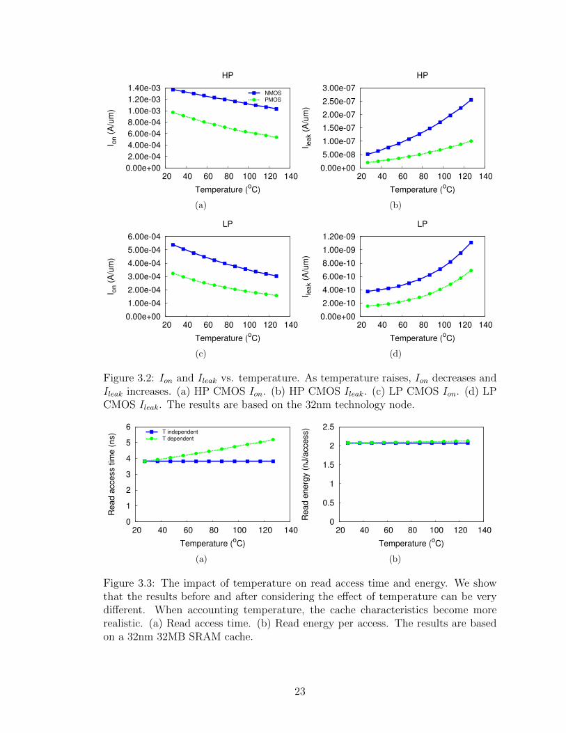
One enhancement to CACTI we made is a comprehensive temperature model.
Both circuit performance and power are temperature dependent: performance de-
grades and leakage power increases with increasing temperature [31]. We show a
few examples of the effect of temperature in Figure 3.2. Note that lower Ion means
slower performance, and higher Ileak means higher leakage power. However, CACTI
only models the dependence of leakage power on temperature. We improve CACTI
by adding an Ion look up table such that the circuit performance and dynamic en-
ergy consumption are also temperature dependent. Figure 3.3 shows the read access
time and energy after accounting the effect of temperature on Ion.
22
0.00e+00
2.00e-04
4.00e-04
6.00e-04
8.00e-04
1.00e-03
1.20e-03
1.40e-03
20 40 60 80 100 120 140
I on (
A/u
m)
Temperature (oC)
HP
NMOS
PMOS
(a)
0.00e+00
5.00e-08
1.00e-07
1.50e-07
2.00e-07
2.50e-07
3.00e-07
20 40 60 80 100 120 140
I lea
k (
A/u
m)
Temperature (oC)
HP
(b)
0.00e+00
1.00e-04
2.00e-04
3.00e-04
4.00e-04
5.00e-04
6.00e-04
20 40 60 80 100 120 140
I on (
A/u
m)
Temperature (oC)
LP
(c)
0.00e+00
2.00e-10
4.00e-10
6.00e-10
8.00e-10
1.00e-09
1.20e-09
20 40 60 80 100 120 140
I lea
k (
A/u
m)
Temperature (oC)
LP
(d)
Figure 3.2: Ion and Ileak vs. temperature. As temperature raises, Ion decreases andIleak increases. (a) HP CMOS Ion. (b) HP CMOS Ileak. (c) LP CMOS Ion. (d) LPCMOS Ileak. The results are based on the 32nm technology node.
0
1
2
3
4
5
6
20 40 60 80 100 120 140
Read a
cce
ss tim
e (
ns)
Temperature (oC)
T independent
T dependent
(a)
0
0.5
1
1.5
2
2.5
20 40 60 80 100 120 140
Read e
nerg
y (
nJ/a
ccess)
Temperature (oC)
(b)
Figure 3.3: The impact of temperature on read access time and energy. We showthat the results before and after considering the effect of temperature can be verydifferent. When accounting temperature, the cache characteristics become morerealistic. (a) Read access time. (b) Read energy per access. The results are basedon a 32nm 32MB SRAM cache.
23

3.1.4 STT-RAM Modeling
The STT-RAM modeling is based on NVSim, a memory modeling tool similar
to CACTI, but which is capable of modeling various non-volatile memories includ-
ing STT-RAM, PCM (phase change memory), ReRAM (resistive RAM), FBDRAM
(floating body dynamic RAM), and NAND flash. For STT-RAM modeling, it re-
quires configurations such as the cell size, SET/RESET pulse width and amplitude,
and the read current.
We project the parameters required by NVSim based on scaling trends shown
in [29] and [23], using the 54nm technology node as the baseline. The projected data
are presented in Table 3.2. Note that we kept the cell feature size and the write
pulse width constant to simplify the projection. Also note that the write pulse width
and amplitude shown correspond to the required write energy that can successfully
write an STT-RAM cell and preserve its state for 10 years. Later in Chapter 5, we
show that a lower write energy is needed if the target data-retention time is shorter.
Table 3.2: STT-RAM parameters.
Technology Feature Write pulse Write ReadNode size (F 2) width (ns) current (uA) current (uA)
54nm 14 10 350 7445nm 14 10 292 6132nm 14 10 207 4422nm 14 10 143 30
3.1.5 Gain Cell eDRAM Modeling
Similar to SRAM, there are many forms of gain cell eDRAM [32–43]. For CPU
cache architectures, both the operating speed and the retention time of a gain cell
24

eDRAM circuit are important. We thus chose the boosted 3T gain cell [40] as the
fundamental cell structure due to its capability to operate at high frequency while
preserving a long data-retention time.
Figure 3.4 shows the schematic of the boosted 3T PMOS gain cell eDRAM. It
is comprised of a write access transistor (PW), a read access transistor (PR), and a
storage transistor (PS). PMOS transistors are utilized because a PMOS device has
less leakage current compared to an NMOS device of the same size. Lower leakage
current enables lower standby power and longer retention time.
RBL
RWL
WBL
WWL
Storage node
PWPS
PR
Figure 3.4: Boosted 3T gain cell schematic.
During write access, the write bit-line (WBL) is driven to the desired voltage
level by the write driver. Additionally, the write word-line (WWL) is driven to a
negative voltage to avoid the threshold voltage drop such that a complete data ‘0’
can be passed through the PMOS write access transistor from WBL to the storage
node.
When performing a read operation, once the read word-line (RWL) is switched
from VDD to 0V, the precharged read bit-line (RBL) is pulled down slightly if a
data ‘0’ is stored in the storage node. If a data ‘1’ is stored in the storage node, RBL
25

remains at the precharged voltage level. The gate-to-RWL coupling capacitance of
PS enables preferential boosting: when the storage node voltage is low, PS is in
inversion mode, which results in a larger coupling capacitance. On the other hand,
when the storage node voltage is high, PS is in weak-inversion mode, which results
in a smaller coupling capacitance. Therefore, when RWL switches from VDD to
0V, a low storage node voltage is coupled down more than a high storage node
voltage. The signal difference between data ‘0’ and data ‘1’ during a read operation
is thus amplified through preferential boosting. This allows the storage node voltage
to decay further before a refresh is needed, which effectively translates to a longer
data-retention time and better read performance. Table 3.3 summarizes the signal
voltages for each operating mode.
Table 3.3: Signals for each operating mode of the boosted 3T gain cell [28].
RWL RBL WWL WBL
Hold VDD VDD VDD 0VWrite 0/1 VDD VDD -500mV 0V/VDDRead 0/1 ∼0V ∼VDD VDD 0V
3.1.5.1 Validation
The gain cell eDRAM model is validated against [28] with respect to latency,
retention time, and refresh power. Our model is based on CACTI utilizing the PTM
65nm LP CMOS technology, while the test chip presented in [28] is fabricated in a
65nm LP CMOS process. Setting the same memory array size, operating voltage
and temperature, our model shows 11% increase in latency and 20% decrease in
retention time. In addition, with the same refresh rate, our model shows 13% more
26

refresh power. These differences are possibly due to implementation differences
between the processes and array organizations. We thus consider our model to be
reasonable.
3.1.5.2 The Impact of PVT Variations
We quantify the correlations between the retention time of gain cell eDRAMs
and PVT variations. We utilize HSPICE and its Monte-Carlo simulation utility
to analyze the retention time variation of a bit cell, where each simulation point
consists of 5,000 samples. To model the process variations, we consider both the
VTH (threshold voltage) variation and the TOX (oxide thickness) variation, as
suggested in [44]. We further model the distribution of a cache line based on the
retention time distribution of a bit cell. Table 3.4 shows the retention times of 45nm,
32nm, and 22nm gain cells we have modeled.
Table 3.4: Gain cell retention time.45nm 32nm 22nm
Retention time 40us 20us 10us
• Process variations. Figure 3.5 shows the gain cell eDRAM retention time
distribution with respect to a range of process variations. We assume both
VTH and TOX follow the Gaussian distribution. The ranges of variances of
VTH and TOX are based on process variations of 32nm CMOS technologies
presented in [45]. From Figure 3.5(a), the retention time distribution of a bit
cell appears as a Gaussian distribution but with the lower tail longer than the
upper tail, meaning only a few samples are in the worst case retention time
27

level. Moreover, the retention time distribution is very sensitive to the process
variations – the larger the variation, the more spread out the distribution.
The retention time distribution of a 64B cache line is reflected by the bit cell
retention time distribution. As a result, when the process variations increase,
the line retention time distribution curve shifts left to a shorter retention
time region with the spread remaining approximately the same, as shown in
Figure 3.5(b).
0 0.02 0.04 0.06 0.08 0.1
0.12 0.14 0.16 0.18 0.2
0 50 100 150 200 250
Fre
quency o
f occurr
en
ce
Retention time (us)
Bit cell
(10%, 5%)(12%, 6%)(14%, 7%)(16%, 8%)(18%, 9%)
(a)
0
0.05
0.1
0.15
0.2
0.25
0.3
0.35
0 20 40 60 80 100 120
Fre
quency o
f occurr
en
ce
Retention time (us)
64 B cache line
(b)
Figure 3.5: Retention time distribution vs. process variations. (a) Bit cell. (b) 64Bcache line. Supply voltage = 1 V; temperature = 75◦C. The percentage numbers inparentheses represent (σV TH/µV TH , σTOX/µTOX)
• Voltage variation. Figure 3.6 shows that the supply voltage variation has
negligible impact on the retention time. For a given gain cell design and supply
voltage, one can exchange faster access time with longer retention time, i.e., a
cell with faster access time has shorter retention time and vice versa. However,
under a higher voltage, although the access time becomes shorter, leakage also
increases. Higher leakage shortens the data-retention time. Faster access time
and higher leakage thus balance each other out, producing near-zero net effect
28

on the cell retention time.
0
0.02
0.04
0.06
0.08
0.1
0.12
0.14
20 40 60 80 100 120 140 160 180 200 220
Fre
qu
en
cy o
f occu
rre
nce
Retention time (us)
Bit cell
0.950V0.975V1.000V1.025V1.050V
(a)
0
0.05
0.1
0.15
0.2
0.25
0.3
20 30 40 50 60 70 80 90 100
Fre
qu
en
cy o
f occu
rre
nce
Retention time (us)
64 B cache line
(b)
Figure 3.6: Retention time distribution vs. voltage variation. (a) Bit cell. (b) 64Bcache line. σV TH/µV TH = 14%, σTOX/µTOX = 7%; temperature = 75◦C.
• Temperature variation. Leakage current is a function of temperature –
leakage increases with increasing temperature. Consequently, the retention
time shortens as the temperature increases, as demonstrated in Figure 3.7.
Since temperature is power dependent, the processor thermal behavior is dif-
ferent for different workloads or execution phases [46]. On-die temperature
sensors are thus required for tuning the refresh rate at run-time.
3.2 Design Space Exploration
Using our cache modeling framework, we compare large SRAM, STT-RAM,
and gain cell eDRAM caches. The design space considered in this section includes
cache size, technology scaling, and temperature. We use the following cache charac-
teristics as the key comparison metrics: read latency (ns), write latency (ns), read
energy (nJ/access), write energy (nJ/access), leakage power (mW), refresh power
29

0
0.02
0.04
0.06
0.08
0.1
0.12
0.14
0.16
20 40 60 80 100 120 140 160 180 200 220
Fre
qu
en
cy o
f occu
rre
nce
Retention time (us)
Bit cell
25oC
35oC
45oC
55oC
65oC
75oC
85oC
95oC
(a)
0
0.05
0.1
0.15
0.2
0.25
0.3
20 30 40 50 60 70 80 90 100
Fre
qu
en
cy o
f occu
rre
nce
Retention time (us)
64 B cache line
(b)
Figure 3.7: Retention time distribution vs. temperature. (a) Bit cell. (b) 64B cacheline. σV TH/µV TH = 14%, σTOX/µTOX = 7%; supply voltage = 1 V.
(mW), and area (mm2)
3.2.1 Memory Technology Comparison
Table 3.5 compares 32nm 32MB caches built with SRAM, STT-RAM, and
eDRAM. We summarize the results as follows:
• Read latency and read energy. Our experiments show that the inter-
connections play a dominant role in access time and access energy for high
capacity caches. As a result, although accessing an SRAM cell requires the
least time (reading an SRAM cell requires less than 1ns; reading an STT-RAM
or an eDRAM cell requires around 2ns [47, 48]), due to the smaller cell sizes
and shorter wires, the STT-RAM and the eDRAM caches have shorter read
latencies and lower read energies compared to the SRAM cache. In particular,
the STT-RAM cache has the smallest cell size and correspondingly best read
performance. In summary, the read latency of the SRAM cache is 1.45X and
1.04X longer than the STT-RAM and eDRAM caches, and its read energy is
30

2.22X and 1.21X higher.
• Write latency and write energy. Due to the long write time and the
high write current requirements for programming an STT-RAM cell, the STT-
RAM cache has much longer write latency and much higher write energy. Our
results show that the STT-RAM cache has around 7X longer write latency
when compared to the SRAM and the eDRAM caches, while requiring more
than 20X energy per write access.
• Standby power. Our results show that the SRAM cache consumes 2.94X and
1.46X more standby power (leakage and refresh together) than the STT-RAM
and the eDRAM caches.
When comparing leakage power, STT-RAM cells and eDRAM cells dissipate
zero/low leakage, therefore the leakage of the STT-RAM and the eDRAM
caches are mainly caused by the peripheral circuitry. On the other hand, in
addition to the peripheral circuitry, SRAM cells also dissipate high leakage.
As a result, the SRAM cache consumes the highest leakage power among the
three memory designs.
In addition to leakage power, eDRAM also consumes refresh power. Note that
although refresh is not required for SRAM and STT-RAM (and hence zero
refresh power), it is advised to scrub STT-RAM periodically to ensure data
correctness. Most research papers ignore the STT-RAM scrubbing overhead.
We also do not consider scrubbing in this work.
31

• Area. Memory cell size is a major factor that determines the area of a cache.
We show that the SRAM cache is around 5X and 2X larger than the STT-RAM
and the eDRAM caches, respectively.
Table 3.5: Detailed characteristics of 32nm 32MB cache designs built with variousmemory technologies.
SRAM STT-RAM Gain cell eDRAM
Read latency 4.45 ns 3.06 ns 4.29 nsWrite latency 4.45 ns 31.77 ns 4.29 nsRetention time - 10 years 20 usRead energy 2.10 nJ/access 0.94 nJ/access 1.74 nJ/accessWrite energy 2.21 nJ/access 47.43 nJ/access 1.79 nJ/accessLeakage power 2105.28 mW 715.38 mW 784.10 mWRefresh power 0 mW 0 mW 600.41 mWArea 80.41 mm2 16.39 mm2 37.38 mm2
Temperature = 75oC
3.2.2 Cache Size
Figure 3.8 and Figure 3.9 compare SRAM, STT-RAM, and eDRAM with
respect to different cache sizes. We also present the detailed numbers in Table 3.6.
As the cache size increases, all the presented metrics also increase. In partic-
ular, since the side effect of adding more SRAM cells is higher leakage, the SRAM
leakage power increases almost proportionally to the growth of capacity. Similarly,
because having more eDRAMs means more refresh operations are required in a given
time, the eDRAM refresh power also increases in proportion with cache size. Lastly,
cache area is proportional to capacity.
Increasing cache size also increases read/write latency and read/write energy.
The added latency and access energy are mainly due to longer access paths, such as
deeper decoders and longer wires.
32

0
1
2
3
4
5
6
16MB 32MB 64MB
Rea
d la
tency (
ns)
Cache size (MB)
SRAM
STT-RAM
eDRAM
(a)
0
5
10
15
20
25
30
35
16MB 32MB 64MB
Write
late
ncy (
ns)
Cache size (MB)
(b)
0
0.5
1
1.5
2
2.5
3
16MB 32MB 64MB
Read e
ne
rgy (
nJ/a
ccess)
Cache size (MB)
(c)
0
5
10
15
20
25
30
35
40
45
50
16MB 32MB 64MB
Write
en
erg
y (
nJ/a
ccess)
Cache size (MB)
(d)
0
500
1000
1500
2000
2500
3000
3500
4000
16MB 32MB 64MB
Leakage p
ow
er
(mW
)
Cache size (MB)
(e)
0
200
400
600
800
1000
1200
1400
16MB 32MB 64MB
Refr
esh
pow
er
(mW
)
Cache size (MB)
(f)
Figure 3.8: Cache characteristics with respect to different memory technologies anddifferent cache sizes. (a) Read latency. (b) Write latency. (c) Read energy. (d)Write energy. (e) Leakage power. (f) Refresh power.
33

0
20
40
60
80
100
120
140
160
16MB 32MB 64MBA
rea (
mm
2)
Cache size (MB)
SRAM
STT-RAM
eDRAM
Figure 3.9: Cache area with respect to different memory technologies and differentcache sizes.
Table 3.6: Detailed characteristics of 32nm cache designs with respect to differentmemory technologies and different cache sizes.
Cache size SRAM STT-RAM eDRAM
Read latency (ns)16MB 3.82 2.64 3.2232MB 4.45 3.06 4.2964MB 5.75 3.69 5.40
Write latency (ns)16MB 3.82 31.49 3.2332MB 4.45 31.77 4.2964MB 5.75 32.22 5.40
Read energy (nJ/access)16MB 1.74 0.78 1.0332MB 2.10 0.95 1.7464MB 2.88 1.22 2.38
Write energy (nJ/access)16MB 1.85 47.26 1.0932MB 2.21 47.43 1.7964MB 3.06 47.70 2.50
Leakage power (mW)16MB 1269.92 536.4 499.1732MB 2105.28 715.38 784.10464MB 3602.26 1228.32 1259.89
Refresh power (mW)16MB 0 0 133.7832MB 0 0 600.4164MB 0 0 1200.82
Area (mm2)16MB 51.42 8.75 18.8332MB 80.41 16.39 37.3864MB 156.90 31.28 105.78
Temperature = 75oC
34

3.2.3 Technology Scaling
Figure 3.10 and Figure 3.11 compare various memory technologies with respect
to different technology nodes (see Table 3.7 for the detailed numbers). As technol-
ogy scales down, smaller device and wire capacitance (i.e., smaller loading) make
transistors easier to drive the next stage. As a result, when using a smaller tech-
nology, both read and write latencies become shorter. Additionally, it is projected
that STT-RAM requires smaller write energy (a function of write time and write
current) at smaller technology nodes; therefore we see a more dramatic decrease in
its write latency and write energy.
Leakage increases as technology scales down. Note that this observation is
based on the assumption that all nodes use the same device technology. For instance,
our 45nm, 32nm, and 22nm are all based on high-k/metal gate CMOS devices. We
expect to see higher performance and lower power at the 22nm node when using a
multi-gate model.
The refresh power trend is less intuitive. Refresh power is mainly determined
by two factors: the retention time and the energy to operate each refresh operation.
As technology scales down, increasing leakage and smaller storage capacitance result
in shorter retention time (Table 3.4), but the energy for each refresh operation also
decreases (Table 3.8), compensating the shortened retention time. We therefore see
a slow increase in refresh power.
35

0
0.5
1
1.5
2
2.5
3
3.5
4
4.5
5
45nm 32nm 22nm
Rea
d la
tency (
ns)
Technology node
SRAM
STT-RAM
eDRAM
(a)
0
5
10
15
20
25
30
35
40
45nm 32nm 22nm
Write
late
ncy (
ns)
Technology node
(b)
0
0.5
1
1.5
2
2.5
3
3.5
4
45nm 32nm 22nm
Read e
ne
rgy (
nJ/a
ccess)
Technology node
(c)
0
10
20
30
40
50
60
70
45nm 32nm 22nm
Write
en
erg
y (
nJ/a
ccess)
Technology node
(d)
0
500
1000
1500
2000
2500
3000
3500
45nm 32nm 22nm
Leakage p
ow
er
(mW
)
Technology node
(e)
0
100
200
300
400
500
600
700
45nm 32nm 22nm
Refr
esh
pow
er
(mW
)
Technology node
(f)
Figure 3.10: Cache characteristics with respect to different memory technologies anddifferent technology nodes. (a) Read latency. (b) Write latency. (c) Read energy.(d) Write energy. (e) Leakage power. (f) Refresh power.
36

0
20
40
60
80
100
120
140
160
180
45nm 32nm 22nmA
rea (
mm
2)
Technology node
SRAM
STT-RAM
eDRAM
Figure 3.11: Cache area with respect to different memory technologies and differenttechnology nodes.
Table 3.7: Detailed characteristics of 32nm cache designs with respect to differentmemory technologies and different technology nodes.
Technology node SRAM STT-RAM eDRAM
Read latency (ns)45nm 4.86 3.36 4.7632nm 4.45 3.06 4.2922nm 4.12 2.85 4.00
Write latency (ns)45nm 4.86 35.24 4.7632nm 4.45 31.77 4.2922nm 5.75 24.59 4.00
Read energy (nJ/access)45nm 3.67 1.66 3.0432nm 2.10 0.95 1.7422nm 1.14 0.52 0.94
Write energy (nJ/access)45nm 3.88 67.52 3.1432nm 2.21 47.43 1.7922nm 1.21 32.78 0.97
Leakage power (mW)45nm 1504.83 492.32 545.2832nm 2105.28 715.38 784.10422nm 3305.42 1161.76 1119.22
Refresh power (mW)45nm 0 0 568.5532nm 0 0 600.4122nm 0 0 609.38
Area (mm2)45nm 160.24 32.43 73.9432nm 80.41 16.39 37.3822nm 38.02 7.77 17.67
Temperature = 75oC
37

Table 3.8: Energy per refresh operation for 32MB eDRAM cache designs.
45nm 32nm 22nm
Energy (nJ/refresh) 0.043 0.023 0.012
Temperature = 75oC
3.2.4 Temperature
The increase in temperature negatively impacts performance and power, shown
in Table 3.9. In particular, as we have illustrated earlier in Figure 3.2, leakage is
highly affected by the temperature. As a result, when the temperature rises from
75oC to 95oC, we observe substantial increase in both the leakage and the refresh
power.
Table 3.9: Detailed characteristics of 32nm 32MB cache designs with respect todifferent memory technologies and different temperatures.
Temperature SRAM STT-RAM eDRAM
Read latency (ns)75oC 4.45 3.06 4.2995oC 4.74 3.29 4.58
Write latency (ns)75oC 4.45 31.77 4.2995oC 4.74 32.32 4.58
Read energy (nJ/access)75oC 2.10 0.95 1.7495oC 2.11 0.96 1.75
Write energy (nJ/access)75oC 2.21 47.43 1.7995oC 2.23 47.44 1.80
Leakage power (mW)75oC 2105.28 715.38 784.10495oC 2990.99 991.72 1064.99
Refresh power (mW)75oC 0 0 600.4195oC 0 0 683.94
38

3.3 Related Work
CACTI is an analytical model that estimates the access time, cycle time, dy-
namic power, leakage power, and area of caches. Originally based on the access time
model presented by Wada et al. [49] and the chip area model presented by Mulder
et al. [50], CACTI 1.0 [51] includes an additional array organizational parameter,
improved peripheral circuit models, a tag array model, and cycle time expressions to
the cache model. In CACTI 2.0 [52], modeling of fully-associative and multiported
caches are supported. Additionally, it is capable of estimating power consumption.
It is also able to capture the effect of technology scaling. CACTI 3.0 [53] further
improves the area and power model. It also supports fully-independent banking of
caches. In eCACTI [54], leakage power is taken into account, which enables more
accurate power estimation. Modeling of leakage power is also included in CACTI
4.0 [55]. Moreover, this version updates the basic circuit structures and device pa-
rameters to reflect advanced technologies. Rodriguez et al. [56] improved CACTI
such that pipelined caches are accurately modeled. As process technologies enter
the deep-submicron era, traditional linear scaling of devices is no longer applicable.
CACTI 5.1 [57] resolves this limitation by adopting the ITRS projected device pa-
rameters at several technology nodes (90nm, 65nm, 45nm, 32nm). Furthermore, it
provides high performance, low standby power, low operating power CMOS mod-
els, embedded DRAM models, and commodity DRAM models. The latest version,
CACTI 6.5 [12], includes advanced interconnection and wire models such that it is
capable of exploring NUCA (non-uniform cache access) and interconnect designs of
39

large caches.
In addition to or based on CACTI, several memory modeling tools were de-
veloped. In particular, Tsai et al. [58] proposed 3DCacti to explore cache design
for 3D architectures. Mohen et al. [59] proposed a power model for NAND flash.
Smullen et al. [21] and Xu et al. [60] explores STT-RAM based cache by imple-
menting STT-RAM models to CACTI. Dong et al. [14] presents NVSim, a tool to
model non-volatile memories. Volelsang et al. [61] proposed a flexible DRAM power
model to analyze a wider range of DRAM architectures. Lee et al. [62] models Fin-
FET and extends CACTI to evaluate FinFET-based caches. Li et al. [63] proposed
CACTI-P, an SRAM cache model that considers advanced leakage reduction tech-
niques. Jouppi et al. [64] proposed CACTI-IO, an extension to CACTI that includes
models for the IO and PHY of the off-chip memory interface.
In this work, we obtain gain cell eDRAM circuit characteristics via HSPICE
simulation using PTM CMOS models. We then integrate gain cell eDRAM to
CACTI. In order to make fair comparisons, we modify CACTI such that the periph-
eral circuitry and SRAM cells also use the same PTM CMOS models. Furthermore,
we use NVSim to obtain the characteristics of STT-RAM subarrays, and integrate
them into CACTI. Finally, we improve the tool such that the effect of temperature
variation is accurately captured.
3.4 Summary
This chapter presents an SRAM, STT-RAM, and eDRAM cache modeling
framework based on CACTI. We describe the framework and the modifications to
40

CACTI in Section 3.1. Specifically, we use HSPICE and PTM CMOS models to
obtain realistic circuit and device characteristics. We also consider the impact of
temperature. Moreover, we integrate a gain cell eDRAM model into the framework.
In Section 3.2, we use the framework to demonstrate a general design space explo-
ration. In particular, we compare large caches built with SRAM, STT-RAM, or
eDRAM, and discuss the impact of cache size, technology scaling, and temperature.
Finally, we review related works in Section 3.3.
41

Chapter 4
Technology Comparison Based on Analytical Models
In the computer architecture field, architecture simulation has been the main-
stream methodology to evaluate architecture and technology tradeoffs. Some archi-
tecture simulators (e.g., full-system simulators) closely reflect real world computer
systems, but they are usually slow and exhibit non-determinism [65]. On the other
hand, although analytical models neglect many implementation details, they are
efficient and in many instances provide reasonable design guidelines. In particu-
lar, when exploring a large design space, analytical models become useful to filter
out less-optimal designs. In this chapter, we present analytical models to compare
caches built with different memory technologies and highlight the key factors that
determine the usefulness of each technology.
4.1 Pipelined Caches
Pipelining is an effective way to improve the data throughput of caches. In this
work, we present a pipeline model for sequentially accessed LLCs. A sequentially
accessed cache saves dynamic power because the data array is accessed only when
a tag is matched. Note that the model can be easily modified for parallel accessed
42

caches. We also assume the cache uses the write allocate policy.
We consider a four-stage pipelined cache:
1. Tag decode, access, and comparison (tag stage): Since accessing the tag array
is usually fast, we assume decoding the tag address, reading the cells, and
comparing the tag are all contained in one stage. In some implementations,
the tag itself is also pipelined.
2. Data decode (dec stage): On a tag match (i.e., a cache hit), the data array will
be accessed by first decoding the address to select the desired cache line. The
depth of the decoder depends on the array size. For a large array partitioned
into multiple banks, the decoder consists of the pre-decoder, the bank decoder,
and the wordline (WL) decoder. If the cache access is a write, we assume data
input and de-multiplexing also happen in the decode stage.
3. Data array access (rd/wr stage): When a WL is enabled, the precharge circuit
is turned off. A differential signal is then generated on a bitline (BL) pair
based on either the cell’s content or the write driver, depending on whether
it is a read operation or a write operation. For a read operation, the sense
amplifiers (SAs) convert the differential signals to digital forms and send them
to the SA latches. After the cells are read or written, the BLs are precharged
and equalized.
4. Multiplexing and data output (out stage): If the cache access is a read, the
SA latched data is further sent to the cache output port via multiplexers.
43

Figure 4.1 shows simplistic representations of four cache access scenarios: read
hit, write hit, read miss, and write miss. Note that when writing to a cache, the
data output stage is skipped. Also note that on a read miss, after fetching data
from the main memory, the fetched data is sent to the CPU/L1/L2 in parallel with
an LLC update. Finally, because we consider a write allocate LLC, on a write miss
the line is first allocated by the main memory, then occurs the write hit action.
tag dec rd out
tag
mem
tag dec wr
tag
mem
tag
Send data to CPU/L1/L2
Send data to CPU/L1/L2
(Update LLC in the background)
Read hit
Also operates data-in and de-multiplexing
(out stage skipped)
Write hit
Write miss
Read miss
wrdec
tag dec wr
Figure 4.1: Simplistic LLC access sequences.
4.2 Model Description
4.2.1 Average Memory Access Latency
We extend the classical average memory access latency (AMAL) equation pre-
sented in Hennessy and Patterson [66] to compute AMAL. It can be approximated
as
AMAL =TMAL
#accesses(4.1)
44

where TMAL represents the total memory access latency, approximated as
TMAL = Tcache + Tmemory (4.2)
and
#accesses = #rdhit + #wrhit + #rdmiss + #wrmiss (4.3)
Tcache and Tmemory are approximated as
Tcache = {#rdhit · (Ttag + Tdec + Trd + Tout)
+ #wrhit · (Ttag + Tdec + Twr)
+ #rdmiss · Ttag
+ #wrmiss · (Ttag + Ttag + Tdec + Twr)} ·1
1−%refresh(4.4)
Tmemory = (#rdmiss + #wrmiss) · Tmem (4.5)
Here rdhit, rdmiss, wrhit, and wrmiss refer to read hit, read miss, write hit, and write
miss; whereas Ttag, Tdec, Trd, Twr, Tout, and Tmem refer to the time each stage (i.e.,
tag, dec, rd, wr, out, and mem stage) requires. Additionally, in Equation 4.4, we
assume normal accesses will be blocked when the cache is under refresh. This only
applies when the cache requires refresh operations, e.g., an eDRAM-based cache.
The model more or less represents the worst case because there is no notion
of parallelism in the model. For instance, if we consider out-of-order accesses or
the effect of using write buffers, AMAL is likely to become shorter. However, the
45

purpose of this model is to serve as a first-order approximation such that designers
can make quick comparisons.
4.2.2 LLC Energy Consumption
We use energy per instruction (EPI ) as the metric to compare LLC energy
consumption. As opposed to the energy required to execute a single instruction, our
definition of EPI is the average amount of energy expended per instruction. This
definition is similar to the EPI representation described in Shao and Brooks [67].
EPI can be expressed as
EPI =Etotal
#instructions(4.6)
where the total energy (Etotal) can be broken down into the active portion
(Eactive) and the standby portion (Estandby), i.e.,
Etotal = Eactive + Estandby (4.7)
Since we are considering a sequentially accessed LLC, Eactive is approximated
as
Eactive = #rdhit · Erd + (#wrhit + #rdmiss + #wrmiss) · Ewr (4.8)
where Erd and Ewr represent the energy consumption of read and write oper-
ations. Note that when a read/write misses, the LLC would request an update from
the main memory. Consequently the main memory would insert a new line to the
46

LLC, resulting in an LLC write.
The standby energy is given by
Estandby = Tsystem · (Pleak + Prefresh) (4.9)
where Tsystem stands for the system execution time, and Pleak, Prefresh stand
for leakage and refresh power, respectively.
In order to express EPI in terms of CPI (cycles per instruction) and API
(LLC accesses per instruction), we further derive Equation 4.6 as follows:
EPI =Eactive
#instructions+
Estandby
#instructions(4.10)
=API
#accesses· Eactive + CPI · Tcycle · (Pleak + Prefresh) (4.11)
where Tcycle is the time period per clock cycle. Because CPI and API are
direct indicators of how intensive an LLC is accessed when executing a workload,
expressing EPI in terms of CPI and API allows us to relate energy usage to workload
behaviors more easily.
4.3 Sensitivity Analysis
In this section, we perform sensitivity studies that compare caches built with
SRAM, STT-RAM, and eDRAM. Specifically, we are interested in the AMAL and
EPI of different technologies, under various LLC read-write ratios, miss ratios, CPIs,
and APIs. We assume both the read miss ratio and the write miss ratio are the same
47

as the total miss ratio. Table 4.1 shows the memory timing and energy properties
used in the experiments.
Table 4.1: Memory properties used in the sensitivity studies.
SRAM STT-RAM eDRAM
Ttag (cycle) 3 3 3Tdec (cycle) 3 1 2Trd (cycle) 1 3 2Twr (cycle) 1 12 2Tout (cycle) 2 1 2Tmem (cycle) 100 100 100%Ref 0% 0% 10%
Erd (nJ) 2 1 2Ewr (nJ) 2 45 2Pleak (mW) 2080 720 800Pref (mW) 0 0 600
4.3.1 Average Memory Access Latency
Figure 4.2 compares the AMAL when using various memory technologies, un-
der different read-write ratios and miss ratios. We summarize the results as follows:
• STT-RAM has shorter read latency but longer write latency, compared to
SRAM and eDRAM. Therefore, when most of the accesses are reads and when
the miss ratio is low, STT-RAM exhibits shorter AMAL. On the other hand,
STT-RAM shows longer AMAL when there are more writes from the CPU
side or more updates from the main memory.
• The AMALs of SRAM and eDRAM decrease with increasing write ratio. This
is because the write latency is shorter than the read latency (i.e., the output
stage is skipped for writes). On the contrary, STT-RAM’s write latency is
longer than its read latency due to its high Twr. Thus, if the miss ratio is
48

low, AMAL increases with increasing write ratio. If the miss ratio is high,
STT-RAM’s shorter read latency produces little benefit because a read miss
requires a write operation (an insertion) from the main memory.
• When the miss ratio increases, Tmem becomes the dominating factor.
0
2
4
6
8
10
12
14
16
0 0.2 0.4 0.6 0.8 1
AM
AL (
cycle
s)
Write ratio
0% miss ratio
SRAM
0
5
10
15
20
25
30
35
40
0 0.2 0.4 0.6 0.8 1
Write ratio
25% miss ratio
STT-RAM
0
10
20
30
40
50
60
0 0.2 0.4 0.6 0.8 1
Write ratio
50% miss ratio
eDRAM
0 10 20 30 40 50 60 70 80 90
0 0.2 0.4 0.6 0.8 1
Write ratio
75% miss ratio
0
20
40
60
80
100
0 0.2 0.4 0.6 0.8 1
Write ratio
100% miss ratio
Figure 4.2: AMAL with respect to (i) various memory technologies; (ii) variousread-write ratios; (iii) various miss ratios. Note that the latency range (Y-axis) ineach of the figures is different.
4.3.2 Energy per Instruction
In addition to read-write ratio and miss ratio, CPI and API are two key
factors that affect the EPI of an LLC. We compare EPI with respect to different
memory technologies, read-write ratios, miss ratios, APIs, and CPIs, as illustrated
in Figure 4.3, 4.4, 4.5, 4.6, and 4.7. The results are summarized as follows:
• Though eDRAM consumes refresh power, due to its lower leakage compared
to SRAM, the EPI of the eDRAM LLC is consistently lower than that of the
SRAM LLC.
• A high write ratio often results in higher STT-RAM EPI when compared to
the EPIs of SRAM and eDRAM. For instance, when the CPI is 1 (Figure 4.5),
49

API is 0.05, and the miss ratio is 0%, STT-RAM has 58% lower EPI than
SRAM if the write ratio is 0 (i.e., all reads), but consumes 109% more EPI
if the write ratio is 1 (i.e., all writes). The write ratio crossing point in this
example is 0.37.
• A high miss ratio is also likely to result in higher STT-RAM EPI. Also con-
sidering the case where CPI is 1, API is 0.05, if all the requests are reads,
STT-RAM has smaller EPI compared to SRAM if the miss ratio is 25% or
lower. However, if the miss ratio is 50% or higher, STT-RAM consumes more
EPI.
• When the LLC accesses per cycle is low, STT-RAM in general dissipates the
lowest power. Note that the LLC accesses per cycle can be expressed in terms
of APICPI
. Using an extreme example, when CPI is 10 and API is 0.01, STT-RAM
is at all times more energy-efficient than SRAM and eDRAM.
4.4 Summary
This chapter presents simplistic analytical models for comparing the AMAL
and the EPI of LLCs built with different memory technologies. The models provide
a first-order design guideline, which enable cache designers to quickly evaluate dif-
ferent technologies. Moreover, based on the models, we conduct sensitivity analysis
and show that read-write ratio, miss ratio, API, and CPI are all important factors
that determine the usefulness of each memory technology.
50

CPI = 0.1
0 0.05 0.1
0.15 0.2
0.25 0.3
0.35 0.4
0.45
AP
I =
0.0
1
EP
I (n
J/insns)
0% miss ratio
SRAM
0 0.05 0.1
0.15 0.2
0.25 0.3
0.35 0.4
0.45
25% miss ratio
STT-RAM
0 0.05 0.1
0.15 0.2
0.25 0.3
0.35 0.4
0.45
50% miss ratio
eDRAM
0 0.05 0.1
0.15 0.2
0.25 0.3
0.35 0.4
0.45
75% miss ratio
0 0.05 0.1
0.15 0.2
0.25 0.3
0.35 0.4
0.45
100% miss ratio
0
0.5
1
1.5
2
AP
I =
0.0
5
EP
I (n
J/insns)
0
0.5
1
1.5
2
0
0.5
1
1.5
2
0
0.5
1
1.5
2
0
0.5
1
1.5
2
0 0.5
1 1.5
2 2.5
3 3.5
4 4.5
AP
I =
0.1
EP
I (n
J/insns)
0 0.5
1 1.5
2 2.5
3 3.5
4 4.5
0 0.5
1 1.5
2 2.5
3 3.5
4 4.5
0 0.5
1 1.5
2 2.5
3 3.5
4 4.5
0 0.5
1 1.5
2 2.5
3 3.5
4 4.5
0
1
2
3
4
5
6
7
8
9
AP
I =
0.2
EP
I (n
J/insns)
0
1
2
3
4
5
6
7
8
9
0
1
2
3
4
5
6
7
8
9
0
1
2
3
4
5
6
7
8
9
0
1
2
3
4
5
6
7
8
9
0
5
10
15
20
25
30
35
40
45
0 0.2 0.4 0.6 0.8 1
AP
I =
1
EP
I (n
J/insns)
Write ratio
0
5
10
15
20
25
30
35
40
45
0 0.2 0.4 0.6 0.8 1
Write ratio
0
5
10
15
20
25
30
35
40
45
0 0.2 0.4 0.6 0.8 1
Write ratio
0
5
10
15
20
25
30
35
40
45
0 0.2 0.4 0.6 0.8 1
Write ratio
0
5
10
15
20
25
30
35
40
45
0 0.2 0.4 0.6 0.8 1
Write ratio
Figure 4.3: EPI (CPI = 0.1) with respect to (i) various memory technologies; (ii)various read-write ratios; (iii) various miss ratios; (iv) various API. Note that thelatency range (Y-axis) in each of the figures is different.
51

CPI = 0.5
0
0.1
0.2
0.3
0.4
0.5
0.6
AP
I =
0.0
1
EP
I (n
J/insns)
0% miss ratio
SRAM
0
0.1
0.2
0.3
0.4
0.5
0.6
25% miss ratio
STT-RAM
0
0.1
0.2
0.3
0.4
0.5
0.6
50% miss ratio
eDRAM
0
0.1
0.2
0.3
0.4
0.5
0.6
75% miss ratio
0
0.1
0.2
0.3
0.4
0.5
0.6
100% miss ratio
0
0.5
1
1.5
2
AP
I =
0.0
5
EP
I (n
J/insns)
0
0.5
1
1.5
2
0
0.5
1
1.5
2
0
0.5
1
1.5
2
0
0.5
1
1.5
2
0 0.5
1 1.5
2 2.5
3 3.5
4 4.5
AP
I =
0.1
EP
I (n
J/insns)
0 0.5
1 1.5
2 2.5
3 3.5
4 4.5
0 0.5
1 1.5
2 2.5
3 3.5
4 4.5
0 0.5
1 1.5
2 2.5
3 3.5
4 4.5
0 0.5
1 1.5
2 2.5
3 3.5
4 4.5
0 1 2 3 4 5 6 7 8 9
AP
I =
0.2
EP
I (n
J/insns)
0 1 2 3 4 5 6 7 8 9
0 1 2 3 4 5 6 7 8 9
0 1 2 3 4 5 6 7 8 9
0 1 2 3 4 5 6 7 8 9
0
5
10
15
20
25
30
35 40
45
0 0.2 0.4 0.6 0.8 1
AP
I =
1
EP
I (n
J/insns)
Write ratio
0
5
10
15
20
25
30
35 40
45
0 0.2 0.4 0.6 0.8 1
Write ratio
0
5
10
15
20
25
30
35 40
45
0 0.2 0.4 0.6 0.8 1
Write ratio
0
5
10
15
20
25
30
35 40
45
0 0.2 0.4 0.6 0.8 1
Write ratio
0
5
10
15
20
25
30
35 40
45
0 0.2 0.4 0.6 0.8 1
Write ratio
Figure 4.4: EPI (CPI = 0.5) with respect to (i) various memory technologies; (ii)various read-write ratios; (iii) various miss ratios; (iv) various API. Note that thelatency range (Y-axis) in each of the figures is different.
52

CPI = 1
0
0.2
0.4
0.6
0.8
1
AP
I =
0.0
1
EP
I (n
J/insns)
0% miss ratio
SRAM
0
0.2
0.4
0.6
0.8
1
25% miss ratio
STT-RAM
0
0.2
0.4
0.6
0.8
1
50% miss ratio
eDRAM
0
0.2
0.4
0.6
0.8
1
75% miss ratio
0
0.2
0.4
0.6
0.8
1
100% miss ratio
0
0.5
1
1.5
2
2.5
AP
I =
0.0
5
EP
I (n
J/insns)
0
0.5
1
1.5
2
2.5
0
0.5
1
1.5
2
2.5
0
0.5
1
1.5
2
2.5
0
0.5
1
1.5
2
2.5
0 0.5
1 1.5
2 2.5
3 3.5
4 4.5
AP
I =
0.1
EP
I (n
J/insns)
0 0.5
1 1.5
2 2.5
3 3.5
4 4.5
0 0.5
1 1.5
2 2.5
3 3.5
4 4.5
0 0.5
1 1.5
2 2.5
3 3.5
4 4.5
0 0.5
1 1.5
2 2.5
3 3.5
4 4.5
0 1 2 3 4 5 6 7 8 9
AP
I =
0.2
EP
I (n
J/insns)
0 1 2 3 4 5 6 7 8 9
0 1 2 3 4 5 6 7 8 9
0 1 2 3 4 5 6 7 8 9
0 1 2 3 4 5 6 7 8 9
0 5
10 15 20 25 30 35 40 45
0 0.2 0.4 0.6 0.8 1
AP
I =
1
EP
I (n
J/insns)
Write ratio
0 5
10 15 20 25 30 35 40 45
0 0.2 0.4 0.6 0.8 1
Write ratio
0 5
10 15 20 25 30 35 40 45
0 0.2 0.4 0.6 0.8 1
Write ratio
0 5
10 15 20 25 30 35 40 45
0 0.2 0.4 0.6 0.8 1
Write ratio
0 5
10 15 20 25 30 35 40 45
0 0.2 0.4 0.6 0.8 1
Write ratio
Figure 4.5: EPI (CPI = 1) with respect to (i) various memory technologies; (ii)various read-write ratios; (iii) various miss ratios; (iv) various API. Note that thelatency range (Y-axis) in each of the figures is different.
53

CPI = 2
0
0.5
1
1.5
2
AP
I =
0.0
1
EP
I (n
J/insns)
0% miss ratio
SRAM
0
0.5
1
1.5
2
25% miss ratio
STT-RAM
0
0.5
1
1.5
2
50% miss ratio
eDRAM
0
0.5
1
1.5
2
75% miss ratio
0
0.5
1
1.5
2
100% miss ratio
0
0.5
1
1.5
2
2.5
AP
I =
0.0
5
EP
I (n
J/insns)
0
0.5
1
1.5
2
2.5
0
0.5
1
1.5
2
2.5
0
0.5
1
1.5
2
2.5
0
0.5
1
1.5
2
2.5
0
1
2
3
4
5
AP
I =
0.1
EP
I (n
J/insns)
0
1
2
3
4
5
0
1
2
3
4
5
0
1
2
3
4
5
0
1
2
3
4
5
0 1 2 3 4 5 6 7 8 9
AP
I =
0.2
EP
I (n
J/insns)
0 1 2 3 4 5 6 7 8 9
0 1 2 3 4 5 6 7 8 9
0 1 2 3 4 5 6 7 8 9
0 1 2 3 4 5 6 7 8 9
0 5
10 15 20 25 30 35 40 45
0 0.2 0.4 0.6 0.8 1
AP
I =
1
EP
I (n
J/insns)
Write ratio
0 5
10 15 20 25 30 35 40 45
0 0.2 0.4 0.6 0.8 1
Write ratio
0 5
10 15 20 25 30 35 40 45
0 0.2 0.4 0.6 0.8 1
Write ratio
0 5
10 15 20 25 30 35 40 45
0 0.2 0.4 0.6 0.8 1
Write ratio
0 5
10 15 20 25 30 35 40 45
0 0.2 0.4 0.6 0.8 1
Write ratio
Figure 4.6: EPI (CPI = 2) with respect to (i) various memory technologies; (ii)various read-write ratios; (iii) various miss ratios; (iv) various API. Note that thelatency range (Y-axis) in each of the figures is different.
54

CPI = 10
0
2
4
6
8
10
AP
I =
0.0
1
EP
I (n
J/insns)
0% miss ratio
SRAM
0
2
4
6
8
10
25% miss ratio
STT-RAM
0
2
4
6
8
10
50% miss ratio
eDRAM
0
2
4
6
8
10
75% miss ratio
0
2
4
6
8
10
100% miss ratio
0
2
4
6
8
10
AP
I =
0.0
5
EP
I (n
J/insns)
0
2
4
6
8
10
0
2
4
6
8
10
0
2
4
6
8
10
0
2
4
6
8
10
0
2
4
6
8
10
AP
I =
0.1
EP
I (n
J/insns)
0
2
4
6
8
10
0
2
4
6
8
10
0
2
4
6
8
10
0
2
4
6
8
10
0
2
4
6
8
10
12
AP
I =
0.2
EP
I (n
J/insns)
0
2
4
6
8
10
12
0
2
4
6
8
10
12
0
2
4
6
8
10
12
0
2
4
6
8
10
12
0 5
10 15 20 25 30 35 40 45
0 0.2 0.4 0.6 0.8 1
AP
I =
1
EP
I (n
J/insns)
Write ratio
0 5
10 15 20 25 30 35 40 45
0 0.2 0.4 0.6 0.8 1
Write ratio
0 5
10 15 20 25 30 35 40 45
0 0.2 0.4 0.6 0.8 1
Write ratio
0 5
10 15 20 25 30 35 40 45
0 0.2 0.4 0.6 0.8 1
Write ratio
0 5
10 15 20 25 30 35 40 45
0 0.2 0.4 0.6 0.8 1
Write ratio
Figure 4.7: EPI (CPI = 10) with respect to (i) various memory technologies; (ii)various read-write ratios; (iii) various miss ratios; (iv) various API. Note that thelatency range (Y-axis) in each of the figures is different.
55

Chapter 5
Low Power Techniques for Caches
In order to make useful comparisons between energy-efficient L3Cs built with
different technologies, we propose to integrate low power techniques either at the
device, circuit level, or at the architecture level. This chapter presents the following:
• We review and summarize low power techniques for SRAM caches.
• We review summarize optimization techniques for improving STT-RAM energy-
efficiency.
• We discuss the impact of refresh on eDRAM LLC power consumption, with
respect to cache size, technology node, process variations, and temperature.
• We classify eDRAM refresh-reduction schemes into two categories and show
that the use of dead-line prediction effectively eliminates unnecessary refreshes.
5.1 Low Power Techniques for SRAM Caches
As CMOS technology scales down to the sub-micron/nanometer region, leak-
age becomes the dominant component of power dissipation. Many low power tech-
niques have been proposed to reduce the leakage power of SRAM caches. We review
56

the commonly known methods as follows:
5.1.1 Device and Circuit Techniques
Leakage reduction circuit techniques either attempt to decrease the supply
voltage (VDD) or to increase the threshold voltage (VTH). For instance, one of the
most widely used low power method is to equip SRAMs with sleep mode capability
by applying power gating [68]. Power gating not only decreases the cross voltage
of SRAM cells, but also increases the VTH of the pull-down/pull-up transistors.
Another popular method is assigning different VTH to each transistor. For instance,
Amelifard et al. [69] applied different VTH and TOX (oxide thickness) for each
SRAM cell to reduce leakage without degrading the performance. Dynamic VTH
control via body biasing also reduces leakage effectively. For instance, Kim et al. [70]
presented a low leakage SRAM cache using forward body biasing.
The most effective power reduction technique is voltage scaling. Applying a
lower supply voltage reduces both the active power and the standby power. For
instance, dynamic voltage scaling reduces leakage power with minimal performance
overhead. Another example is near-threshold computing, which refers to operating
the circuits at ultra-low voltage (VDD close to VTH). Near-threshold computing
reduces energy on the order of 10X but introduces degraded performance and in-
creased functional failure [71]. For example, Pawloski et al. [72] and Fick et al. [73]
demonstrate near-threshold processors that have extremely low energy consumption.
57

5.1.2 Architecture Techniques
Architecture techniques for leakage power reduction attempt to identify the
unused parts of the cache and turn off these parts or put them in low power mode.
Albonesi [74] proposed selective cache ways, which disables a subset of the ways in a
set associative cache when less cache capacity is needed. Kaxiras et al. [75] proposed
cache decay, which uses a time-based dead-line prediction mechanism to turn off
cache lines that hold data not likely to be reused. Flautner et al. [76] proposed
drowsy cache, which periodically put cache lines into a low power yet state-preserving
mode. They show significant leakage power reduction with negligible performance
loss.
5.2 Low Power Techniques for STT-RAM Caches
Due to the scalability of STT-RAM, it is possible to implement LLCs with
higher density, although unlike SRAM or eDRAM, STT-RAM is still under devel-
opment. Since the STT-RAM write operation requires high energy, most low power
techniques for STT-RAM caches focus on write energy reduction. We review several
methods as follows:
5.2.1 Device and Circuit Techniques
Many studies focused on optimizing the STT-RAM cell to minimize the write
latency and the write energy. For instance, Xu et al. [60] showed that one can
sacrifice read latency for better write latency by tuning the access transistor. They
58

further proposed the dual-write speed method that reduces STT-RAM cache energy
consumption. Smullen et al. [21] proposed device optimization methods to relax the
MTJ non-volatility for shorter write time and lower write current. In other words,
they proposed a STT-RAM cache that requires low write energy but needs to be
refreshed (scrubbed) periodically. Nigam et al. [77] proposed using low saturation
magnetization ferromagnetic material to reduce the write energy. Additionally, Zhou
et al. [78] proposed a circuit technique, the early write termination scheme, that
reduces the number of write operations.
5.2.2 Architecture Techniques
Since SRAM has low write power while STT-RAM has negligible leakage, re-
searchers have suggested building hybrid caches that have the SRAM low write
power and the STT-RAM low leakage properties. Specifically, Wu et al. [79] pro-
posed hybrid 2D and 3D cache implementations based on SRAM, eDRAM, STT-
RAM and PCM. Jadidi et al. [80] proposed a hybrid SRAM, STT-RAM cache
with write intensive block detection that remaps cache lines to optimize power con-
sumption. Chen et al. [81] proposed a hybrid cache with low power modes that is
dynamically reconfigured to enable better power efficiency.
Based on relaxed non-volatility STT-RAMs, Sun et al. [82] proposed building
STT-RAM caches that have multiple retention level. They also proposed a refresh
scheme and a data migration scheme that optimize the power and performance of
the entire CPU cache hierarchy. Jog et al. [23] proposed cache revive, which uses
a simple yet efficient refresh scheme for volatile STT-RAM-based caches. It should
59

be noted that the retention failure in STT-RAM is a stochastic process [24]. This
means unlike DRAM, where its capacitor gradually loses electrical charge, an STT-
RAM bit-flip happens instantaneously. Consequently, using DRAM-style refresh
will not provide any reliability for STT-RAM, as it will only read and write back
erroneous value.
5.3 Low Power Techniques for eDRAM Caches
We start this section by highlighting the impact of refresh on eDRAM L3C
energy consumption. We then review refresh management techniques. Finally, we
present a refresh reduction technique based on a practical, low-cost dynamic dead-
line prediction scheme. We use MARSS [15], and workloads from PARSEC [16] and
NPB [17] to conduct the experiments (see Chapter 6 for detail). The eDRAM power
and performance parameters are based on the gain cell eDRAM CACTI results
presented in Chapter 3.
5.3.1 The Impact of Refresh
• Cache size. The dynamic energy, leakage power, and the refresh power of
an LLC increase with increasing cache size. In particular, since the retention
time is independent of the cache organization, more refresh operations are
required for a higher capacity cache within the same refresh period. As a result,
as the number of cache lines increases, refresh power becomes the primary
source of LLC power dissipation. Our results indicate that on average, refresh
contributes to 31% of the power dissipation for a 16MB LLC, whereas for a
60

64MB LLC, the percentage refresh power increases to 52%.
• Technology scaling. As technology scales down, caches become smaller,
faster, and consume less active energy. For instance, a 32nm cache is around
50% smaller than a 45nm cache, while a 22nm cache is also around 50% smaller
than a 32nm cache. However, both subthreshold and gate leakages increase
significantly with decreasing feature size. The increasing leakage coupled with
smaller cell storage capacitance results in shorter retention time. Correspond-
ingly, the LLC leakage and refresh power become worse in smaller technolo-
gies. Based on our simulation results, as the technology node decreases from
45nm to 22nm, the percentage refresh power relative to the total LLC power
increases from 33% to 48%.
• Process variations. Process variation (PV) affects the retention time of
a DRAM cell, whereas the refresh rate is determined by the weakest cells
(i.e., cells that have the shortest data-retention time). For instance, when
PV is small (σV TH/µV TH = 10%, σTOX/µTOX = 5%), the retention time is
around 40us; when PV is medium (σV TH/µV TH = 14%, σTOX/µTOX = 7%),
the retention time decreases to 20us; finally, when PV is large (σV TH/µV TH
= 10%, σTOX/µTOX = 9%), the retention time becomes 10us. Therefore, as
PV becomes more severe, a faster refresh rate is required, resulting in higher
refresh power. For example, an eDRAM cache under medium PV and large
PV dissipates 2X and 4X higher refresh power, respectively, when compared
to an eDRAM under small PV.
61

• Temperature. High temperature results in higher leakage, and therefore
shorter eDRAM data-retention time. For instance, at 75oC, the retention time
of our eDRAM model is 20us, whereas at 95oC, the retention time decreases to
18us. Subsequently, at 95oC the eDRAM cache requires 11.5% faster refresh
rate, which also results in 11.5% higher refresh power.
5.3.2 Refresh Management
Refresh is required for eDRAM-based caches. Unfortunately, this creates neg-
ative impacts on both performance and power. For instance, the cache bandwidth
is degraded by refresh activity because normal cache accesses are stalled while the
cache is being refreshed. This problem can be alleviated by organizing a cache into
multiple sub-banks, allowing refresh operations and normal cache accesses to happen
concurrently [83].
There are several methods to mitigate refresh penalties. They can be classified
into two categories:
1. Reducing the refresh rate by exploiting process and temperature
variations. Process and temperature variations affect the retention time of
a DRAM cell. Traditionally, the refresh rate is determined by the weakest
DRAM cells, i.e., those cells that have the shortest data-retention time. How-
ever, conservatively performing refresh operations based on the shortest re-
tention time introduces significant refresh overhead. One promising approach
for reducing refresh is to utilize retention-time variation and to decrease the
refresh rates for blocks or rows that exhibit longer retention time [84–87]. This
62

approach requires an initial time period to characterize the retention time of
each individual memory block and store the retention time information in a
table.
Another promising approach is to utilize error-correcting codes (ECC) to dy-
namically detect and correct bits that fail [88–90]. This approach reduces the
refresh rate by disassociating failure rate from single effects of the weakest
cells.
2. Reducing the number of refresh operations by exploiting memory-
access behaviors. Reohr [91] presents several approaches for refreshing
eDRAM-based caches, including periodic refresh, line-level refresh based on
time stamps, and no-refresh. For instance, Liang et al. [92] showed that by
adopting the line-level refresh or the no-refresh approaches with intelligent
cache-replacement policies, 3T1D (three transistors one diode) eDRAM be-
comes a potential substitute for SRAM in the context of L1 data caches.
The periodic refresh policy does a sweep of the cache such that all cache lines
are refreshed periodically, similar to the refresh mechanism used in regular
DRAM main memories. It introduces the least logic and storage overhead but
provides no opportunity to reduce the number of refresh operations.
The line-level refresh policy utilizes line-level counters to track the refresh
status of each cache line. This policy is analogous to Smart Refresh [93], a
refresh-management framework for DRAM main memories. When a line is
refreshed, its counter resets to zero. There are two types of refreshes: the
63

implicit refresh and the explicit refresh. An implicit refresh happens when
the line is read, written, or loaded; an explicit refresh happens when the line-
level counter signals a refresh to the data array. Therefore, if two accesses to
the same cache line occur within a refresh period, the cache line is implicitly
refreshed and no explicit refresh is needed.
The no-refresh policy never refreshes the cache lines. Similar to the line-level
refresh implementation, each cache line has a counter that tracks the time
after an implicit refresh. When the counter reaches the retention time, the
line is marked as invalid. As a result, the no-refresh policy removes refresh
power completely but potentially introduces more cache misses.
Our refresh reduction method falls into the second category: we attempt
to identify dead lines using a low-cost dynamic dead-line prediction scheme and,
thereby, to eliminate refreshes to these lines. To our knowledge, this is the first
work that uses dead-line prediction to reduce the refresh power of eDRAM-based
caches. Our design can also be applied on top of variable retention time architectures
or error-correcting systems.
5.3.3 Dead-Line Prediction vs. Refresh
Refresh is the main source of eDRAM-based L3C power dissipation [89]. Pre-
vious studies have shown the effectiveness of using dead-line prediction to reduce
the leakage power of SRAM-based L1 or L2 caches. However, to the best of our
knowledge, no previous study has demonstrated dead-line prediction in the context
64

of eDRAM caches. This work proposes a refresh-reduction method for eDRAM L3Cs
using a low-cost dynamic dead-line prediction scheme. If a cache line is predicted
dead, refresh to the line is skipped, thereby minimizing refresh energy. Additionally,
using dead-line prediction to reduce standby power is a more natural fit for eDRAM
than SRAM. For instance, unlike SRAM-based cache lines, re-enabling eDRAM-
based lines does not require wake-up time. Moreover, since hardware such as a
ring oscillator and refresh pulse generator are already part of the eDRAM refresh
controller, we can reuse them to support time-based dead-line predictors.
To demonstrate the potential refresh power savings that one can achieve by
eliminating refreshes to dead lines, we characterize the average dead time of a cache
line in a 32MB LLC. Based on the workloads considered, on average a cache line is
dead 59% of the time, indicating that significant refresh power can be saved without
degrading performance.
5.3.3.1 Cache Time Durations
Dead-line prediction can be used to improve cache hit rate [94] or to reduce
cache standby power [75]. It uses the concept of cache-time durations, which are
best expressed using the generational behavior of cache lines. Each generation be-
gins with a data insertion and ends with data eviction. A cache-line generation is
partitioned into two parts. The first part, live time, is the time where the line is
actively accessed. The second part, dead time, is the time where the line is await-
ing eviction. Additionally, the access interval is the time between two successful
line references, while the reload interval is the time between two generations of the
65

same line. An example of the generational behavior of a cache line is depicted in
Figure 5.1.
A
Load A
A A A
Access interval
B
Evict A
Load B
B A
Evict B
Reload A
Live time Dead time
Reload interval
Time
Figure 5.1: Generational behavior of a cache line. The generation of A© begins whenit is loaded and ends when it is evicted.
5.3.3.2 Dead Time Characterization
In this section, we characterize the average dead time ratio of each workload
using MARSS [15], a cycle-accurate full-system simulator (see Chapter 6 for more
detail). The results are shown in Figure 5.2 and Figure 5.3. Dead time ratio is
defined as the ratio of the average dead time to the system execution time, i.e.,
Dead time ratio =Average dead time
System execution time(5.1)
It is mainly affected by two factors:
• Memory footprint. If the memory footprint is smaller than the LLC size,
a portion of the LLC lines is unused, which means that these unused lines
are always dead. The memory footprint of each workload and input set is
presented in Appendix A.
66

• LLC miss ratio or MPKI. If the LLC frequently misses, cache lines are
often awaiting for eviction, which means that they have long dead times. The
LLC miss ratio and MPKI (misses per kilo instruction) of each workload and
input set is presented in Appendix A.
5.3.3.3 Dead-Line Prediction
There are several state-of-the-art approaches that use dead-line prediction to
save the leakage power of L1 or L2 SRAM caches. For instance, Kaxiras et al. [75]
proposed two methods to implement time-based leakage control (Cache Decay). The
first method uses a fixed decay interval, which only requires two extra bits for each
cache line to track the decay interval. The decay interval is the elapsed time in which
a cache line has not been accessed. However, since different applications may have
different decay intervals, this method does not always result in optimal standby
power reduction. The second method improves upon the first one by adaptively
finding the optimal decay interval for each of the cache lines. It requires six extra
bits for each line: two bits used as a per-line counter to identify the best decay
interval, and four bits to represent the length of the interval.
One downside is that using counters to forecast decay intervals potentially
results in more false predictions [95]. For example, if the period between two con-
secutive hits is longer than the counters threshold, dead-line prediction is falsely
considered successful. Consequently, instead of prolonging the decay interval to cor-
rect the false prediction, the interval is decreased, making the next prediction also
possibly incorrect.
67

0 0.1 0.2 0.3 0.4 0.5 0.6 0.7 0.8 0.9
1
16
MB
32
MB
64
MB
16
MB
32
MB
64
MB
16
MB
32
MB
64
MB
16
MB
32
MB
64
MB
16
MB
32
MB
64
MB
Avera
ge
dea
d t
ime
ratio
PARSEC simsmall
meanfreqminefacesimcannealbodytrack
(a)
0
0.1
0.2
0.3
0.4
0.5
0.6
0.7
0.8
0.9
16M
B
32M
B
64M
B
16M
B
32M
B
64M
B
16M
B
32M
B
64M
B
16M
B
32M
B
64M
B
16M
B
32M
B
64M
B
Avera
ge d
ead tim
e r
atio
PARSEC simmedium
meanfreqminefacesimcannealbodytrack
(b)
0 0.1 0.2 0.3 0.4 0.5 0.6 0.7 0.8 0.9
1
16M
B
32M
B
64M
B
16M
B
32M
B
64M
B
16M
B
32M
B
64M
B
16M
B
32M
B
64M
B
16M
B
32M
B
64M
B
Avera
ge d
ead tim
e r
atio
PARSEC simlarge
meanfreqminefacesimcannealbodytrack
(c)
Figure 5.2: Average dead time ratio vs. LLC size. (a) PARSEC simsmall. (b)PARSEC simmedium. (c) PARSEC simlarge.
68

0 0.1 0.2 0.3 0.4 0.5 0.6 0.7 0.8 0.9
1
16
MB
32
MB
64
MB
16
MB
32
MB
64
MB
16
MB
32
MB
64
MB
16
MB
32
MB
64
MB
16
MB
32
MB
64
MB
Avera
ge
dea
d t
ime
ratio
NPB class A
meanisftcgbt
(a)
0 0.1 0.2 0.3 0.4 0.5 0.6 0.7 0.8 0.9
1
16M
B
32M
B
64M
B
16M
B
32M
B
64M
B
16M
B
32M
B
64M
B
16M
B
32M
B
64M
B
16M
B
32M
B
64M
B
Avera
ge d
ead tim
e r
atio
NPB class B
meanisftcgbt
(b)
0 0.1 0.2 0.3 0.4 0.5 0.6 0.7 0.8 0.9
1
16M
B
32M
B
64M
B
16M
B
32M
B
64M
B
16M
B
32M
B
64M
B
16M
B
32M
B
64M
B
16M
B
32M
B
64M
B
Avera
ge d
ead tim
e r
atio
NPB class C
meanisftcgbt
(c)
Figure 5.3: Average dead time ratio vs. LLC size. (a) NPB class A. (b) NPB classB. (c) NPB class C.
69

Zhou et al. [96] proposed Adaptive Mode Control, in which a global register
indicates the optimal decay interval for the entire cache. It introduces only a small
storage and power overhead, but it also results in non-optimal cache performance
and power because not every cache line has the same decay interval.
Abella et al. [95] proposed IATAC, a smart predictor to turn off L2 cache
lines, which uses global predictors in addition to local predictors to improve the
prediction accuracy. However, this scheme requires non-negligible overhead, making
it less practical for large caches. For example, a 32MB cache requires on the order
of 10% storage overhead.
In addition to time-based dead-line predictors, Lai et al. [97] proposed a trace-
based dead-line predictor for L1 data caches, Khan et al. [98] proposed sampling
dead-line prediction for LLCs. They demonstrate that by using dead-line prediction,
prefetching can be performed more effectively, hence improving cache hit ratio.
Though a number of dead-line predictors are applicable to eDRAM L3C refresh
reduction, our design inherits the concept from time-based dead-line predictors. It is
easy to implement and introduces insignificant logic and storage overhead. We show
that the proposed implementation effectively reduces eDRAM L3C refresh power.
5.3.3.4 Proposed Implementation
Figure 5.4 shows the proposed eDRAM cache architecture with dynamic dead-
line prediction. It consists of the eDRAM refresh manager, the dynamic dead-line
prediction utility, the SRAM tag array, the eDRAM data array, and other logic and
storage necessary for caches. The temperature sensor determines the frequency of
70

the ring oscillator: higher temperature normally results in higher frequency. This
frequency then determines the rate of the refresh pulse. Additionally, each line has
its time-based dead-line predictor and disable bit. The disable bit is an indicator
of whether the eDRAM line holds valid data or stale data. For instance, if a line is
marked as dead, its content becomes stale after a retention time period has elapsed
because no refreshes were applied. Each set also has a prediction indicator, which
dynamically controls the dead-line predictors based on the history of prediction.
SRAM tag array
Va
lid b
it
Dis
ab
le b
it
De
ad
lin
e p
red
icto
r
Dyn
am
ic p
red
ictio
n
ind
ica
tor
Skip
refresh?
Ro
w d
eco
de
r a
nd
drive
r
eDRAM data array
Match && disable?
Evict && disable?
False prediction
True prediction
Temperature
sensor
Ring
oscillator
Refresh pulse
generator
Cache line pointer
generator
eDRAM
refresh
manager
Way 0
Figure 5.4: Proposed eDRAM cache architecture with dynamic dead-line prediction.
Under normal conditions, an eDRAM cache line is periodically refreshed. How-
ever, if the associated dead-line predictor turns off the line, any refresh signal to the
line is bypassed, disabling refresh. Figure 5.5(a) illustrates the state machine of the
dynamic prediction indicator. A false prediction (F) indicates that the previous des-
ignated decay interval was too short, and a longer interval should be utilized instead
71

to avoid unwanted cache misses. On the other hand, a true prediction (T) indicates
that a reasonable decay interval has been reached. Finally, if many false predictions
are detected, the prediction indicator switches off the dead-line predictors to prevent
more undesired cache misses.
I0 I1 I2 I3 I4 I5 I6
reset
F
T
F
T
F
T
F
T
F
T
F
T
(a)
S0 S7 S6 S5 S4 S3TIME TIME TIME TIME
S1 S2
access
access
access
access
access
access
TIME
retention_timeI0 && TIME
I5 && TIME
I4 && TIME
I3 && TIME
I2 && TIME
I1 && TIMES0: LIVE
S1: DEAD
S2: DISABLE
S3~S7: INTERMEDIATE
(Depend on the indicator
states I1~I5)
(b)
Figure 5.5: Proposed dynamic dead-line prediction implementation. It is comprisedof the dynamic prediction indicator and the dead-line predictor. The dynamic pre-diction indicator determines the decay interval of the dead-line predictor. (a) Statemachine of the dynamic prediction indicator. When the indicator enters state I6,the associated dead-line predictors are turned off to prevent more undesired cachemisses. (b) State machine of the dead-line predictor. In our implementation, TIME= 512 * retention time.
Figure 5.5(b) shows the state machine of the dead-line predictor. Anytime a
line hit or a line insertion happens, the cache line returns to the S0 state, indicating
that the line is alive. When a predetermined time period (TIME) has elapsed,
72
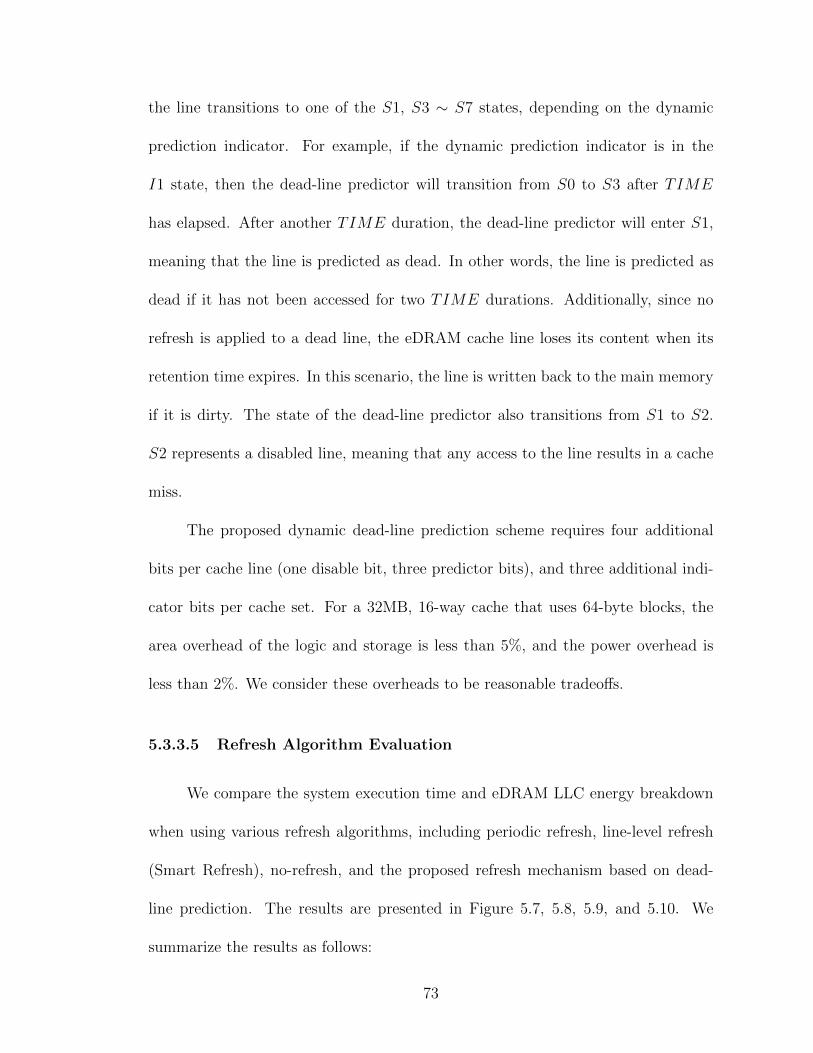
the line transitions to one of the S1, S3 ∼ S7 states, depending on the dynamic
prediction indicator. For example, if the dynamic prediction indicator is in the
I1 state, then the dead-line predictor will transition from S0 to S3 after TIME
has elapsed. After another TIME duration, the dead-line predictor will enter S1,
meaning that the line is predicted as dead. In other words, the line is predicted as
dead if it has not been accessed for two TIME durations. Additionally, since no
refresh is applied to a dead line, the eDRAM cache line loses its content when its
retention time expires. In this scenario, the line is written back to the main memory
if it is dirty. The state of the dead-line predictor also transitions from S1 to S2.
S2 represents a disabled line, meaning that any access to the line results in a cache
miss.
The proposed dynamic dead-line prediction scheme requires four additional
bits per cache line (one disable bit, three predictor bits), and three additional indi-
cator bits per cache set. For a 32MB, 16-way cache that uses 64-byte blocks, the
area overhead of the logic and storage is less than 5%, and the power overhead is
less than 2%. We consider these overheads to be reasonable tradeoffs.
5.3.3.5 Refresh Algorithm Evaluation
We compare the system execution time and eDRAM LLC energy breakdown
when using various refresh algorithms, including periodic refresh, line-level refresh
(Smart Refresh), no-refresh, and the proposed refresh mechanism based on dead-
line prediction. The results are presented in Figure 5.7, 5.8, 5.9, and 5.10. We
summarize the results as follows:
73

• In contrast to utilizing line-level refresh for L1 caches or Smart Refresh for
commodity DRAM main memories, applying line-level refresh to LLCs results
in slightly higher energy usage compared to the baseline periodic refresh. This
is because line-level refresh only improves refresh under the condition that
the retention time of each line is much longer than the line access interval.
However, the retention time is oftentimes shorter than the line access interval,
making the line-level refresh policy unlikely to reduce the number of refresh
operations. Line-level refresh also shortens the refresh period to accommodate
the worst-case scenario in which all lines in a subarray reach the refresh thresh-
old simultaneously. As a result, since the LLC is not as intensively accessed
as the L1 caches, and the data-retention time of eDRAMs is much shorter
than the retention time of commodity DRAMs, line-level refresh introduces
no benefit to LLC refresh reduction.
• Similar to line-level refresh, no-refresh has little opportunity to take advantage
of implicit refresh. Consequently, most cache lines become invalid before they
are re-referenced. Therefore, although no-refresh results in the least LLC
energy consumption, it degrades the system performance significantly (19%
on average). It also results in more system energy consumption due to longer
execution time and higher main memory activity for servicing the additional
cache misses.
• Our proposed refresh scheme reduces refresh power significantly for most of the
workloads considered. On average, the proposed scheme reduces the refresh
74

energy by 42% and reduces the LLC energy by 18%, with 1.1% longer execution
time compared to periodic refresh. Figure 5.6 summarizes the average system
performance and LLC energy of each refresh algorithm.
0.6
0.8
1
1.2
1.4
0.6 0.8 1 1.2 1.4
Norm
aliz
ed
syste
me
xecu
tio
n tim
e
Normalized LLC energy consumption
System execution timevs. LLC energy consumption
Pareto Frontier
PeriodicLine-levelNo-refreshProposed
Figure 5.6: Pareto frontier analysis of different refresh algorithms.
5.4 Summary
This chapter summarizes low power techniques for SRAM, STT-RAM and
eDRAM caches. In particular, we illustrate the significance of refresh on eDRAM
L3C energy consumption, and categorize eDRAM refresh-reduction schemes. At
the end of this chapter, we demonstrate a refresh reduction technique based on
a practical low-cost dynamic dead-line prediction scheme. The refresh reduction
technique is compared against prior arts, and is shown to reduce eDRAM LLC
refresh energy by 42% with minimal performance and area overhead.
75

0
0.2
0.4
0.6
0.8
1
1.2
1.4
Lin
e-le
vel
No
rmaliz
ed
syste
mexe
cu
tion
tim
e
PARSEC simsmall
Pareto Frontier
meanfreqminefacesimcannealbodytrack
(a)
0 0.2 0.4 0.6 0.8
1 1.2 1.4 1.6 1.8
Periodic
Lin
e-level
No-r
efr
esh
Pro
posed
Periodic
Lin
e-level
No-r
efr
esh
Pro
posed
Periodic
Lin
e-level
No-r
efr
esh
Pro
posed
Periodic
Lin
e-level
No-r
efr
esh
Pro
posed
Periodic
Lin
e-level
No-r
efr
esh
Pro
posed
Norm
aliz
ed s
yste
mexecution tim
e
PARSEC simmedium
meanfreqminefacesimcannealbodytrack
(b)
0 0.2 0.4 0.6 0.8
1 1.2 1.4 1.6 1.8
Periodic
Lin
e-level
No-r
efr
esh
Pro
posed
Periodic
Lin
e-level
No-r
efr
esh
Pro
posed
Periodic
Lin
e-level
No-r
efr
esh
Pro
posed
Periodic
Lin
e-level
No-r
efr
esh
Pro
posed
Periodic
Lin
e-level
No-r
efr
esh
Pro
posed
Norm
aliz
ed s
yste
mexecution tim
e
PARSEC simlarge
meanfreqminefacesimcannealbodytrack
(c)
Figure 5.7: Performance evaluation for different refresh algorithms. (a) PARSECsimsmall. (b) PARSEC simmedium. (c) PARSEC simlarge. The proposed refreshalgorithm introduces negligible performance overhead.
76

0 0.2 0.4 0.6 0.8
1 1.2 1.4 1.6 1.8
Pe
rio
dic
Lin
e-le
vel
No-r
efr
esh
Pro
pose
d
Pe
rio
dic
Lin
e-le
vel
No-r
efr
esh
Pro
pose
d
Pe
rio
dic
Lin
e-le
vel
No-r
efr
esh
Pro
pose
d
Pe
rio
dic
Lin
e-le
vel
No-r
efr
esh
Pro
pose
d
Pe
rio
dic
Lin
e-le
vel
No-r
efr
esh
Pro
pose
d
Norm
aliz
ed s
yste
mexe
cutio
n t
ime
NPB class A
meanisftcgbt
(a)
0
0.2
0.4
0.6
0.8
1
1.2
1.4
Periodic
Lin
e-level
No-r
efr
esh
Pro
posed
Periodic
Lin
e-level
No-r
efr
esh
Pro
posed
Periodic
Lin
e-level
No-r
efr
esh
Pro
posed
Periodic
Lin
e-level
No-r
efr
esh
Pro
posed
Periodic
Lin
e-level
No-r
efr
esh
Pro
posed
Norm
aliz
ed s
yste
mexecution tim
e
NPB class B
meanisftcgbt
(b)
0
0.2
0.4
0.6
0.8
1
1.2
1.4
Periodic
Lin
e-level
No-r
efr
esh
Pro
posed
Periodic
Lin
e-level
No-r
efr
esh
Pro
posed
Periodic
Lin
e-level
No-r
efr
esh
Pro
posed
Periodic
Lin
e-level
No-r
efr
esh
Pro
posed
Periodic
Lin
e-level
No-r
efr
esh
Pro
posed
Norm
aliz
ed s
yste
mexecution tim
e
NPB class C
meanisftcgbt
(c)
Figure 5.8: Performance evaluation for different refresh algorithms. (a) NPB classA. (b) NPB class B. (c) NPB class C.
77

0
0.2
0.4
0.6
0.8
1
1.2
Pe
rio
dic
Lin
e-le
vel
No-r
efr
esh
Pro
pose
d
Pe
rio
dic
Lin
e-le
vel
No-r
efr
esh
Pro
pose
d
Pe
rio
dic
Lin
e-le
vel
No-r
efr
esh
Pro
pose
d
Pe
rio
dic
Lin
e-le
vel
No-r
efr
esh
Pro
pose
d
Pe
rio
dic
Lin
e-le
vel
No-r
efr
esh
Pro
pose
d
No
rmaliz
ed
LLC
en
erg
y
PARSEC simsmall
Dynamic Leakage Refresh
meanfreqminefacesimcannealbodytrack
(a)
0
0.2
0.4
0.6
0.8
1
1.2
Periodic
Lin
e-level
No-r
efr
esh
Pro
posed
Periodic
Lin
e-level
No-r
efr
esh
Pro
posed
Periodic
Lin
e-level
No-r
efr
esh
Pro
posed
Periodic
Lin
e-level
No-r
efr
esh
Pro
posed
Periodic
Lin
e-level
No-r
efr
esh
Pro
posed
Norm
aliz
ed L
LC
energ
y
PARSEC simmedium
meanfreqminefacesimcannealbodytrack
(b)
0
0.2
0.4
0.6
0.8
1
1.2
Periodic
Lin
e-level
No-r
efr
esh
Pro
posed
Periodic
Lin
e-level
No-r
efr
esh
Pro
posed
Periodic
Lin
e-level
No-r
efr
esh
Pro
posed
Periodic
Lin
e-level
No-r
efr
esh
Pro
posed
Periodic
Lin
e-level
No-r
efr
esh
Pro
posed
Norm
aliz
ed L
LC
energ
y
PARSEC simlarge
meanfreqminefacesimcannealbodytrack
(c)
Figure 5.9: Energy evaluation for different refresh algorithms. (a) PARSEC sims-mall. (b) PARSEC simmedium. (c) PARSEC simlarge. The proposed refresh algo-rithm effectively reduces the refresh energy and the LLC energy.
78

0
0.2
0.4
0.6
0.8
1
1.2
Pe
rio
dic
Lin
e-le
vel
No-r
efr
esh
Pro
pose
d
Pe
rio
dic
Lin
e-le
vel
No-r
efr
esh
Pro
pose
d
Pe
rio
dic
Lin
e-le
vel
No-r
efr
esh
Pro
pose
d
Pe
rio
dic
Lin
e-le
vel
No-r
efr
esh
Pro
pose
d
Pe
rio
dic
Lin
e-le
vel
No-r
efr
esh
Pro
pose
d
No
rmaliz
ed
LLC
en
erg
y
NPB class A
Dynamic Leakage Refresh
meanisftcgbt
(a)
0
0.2
0.4
0.6
0.8
1
1.2
Periodic
Lin
e-level
No-r
efr
esh
Pro
posed
Periodic
Lin
e-level
No-r
efr
esh
Pro
posed
Periodic
Lin
e-level
No-r
efr
esh
Pro
posed
Periodic
Lin
e-level
No-r
efr
esh
Pro
posed
Periodic
Lin
e-level
No-r
efr
esh
Pro
posed
Norm
aliz
ed L
LC
energ
y
NPB class B
meanisftcgbt
(b)
0
0.2
0.4
0.6
0.8
1
1.2
Periodic
Lin
e-level
No-r
efr
esh
Pro
posed
Periodic
Lin
e-level
No-r
efr
esh
Pro
posed
Periodic
Lin
e-level
No-r
efr
esh
Pro
posed
Periodic
Lin
e-level
No-r
efr
esh
Pro
posed
Periodic
Lin
e-level
No-r
efr
esh
Pro
posed
Norm
aliz
ed L
LC
en
erg
y
NPB class C
meanisftcgbt
(c)
Figure 5.10: Energy evaluation for different refresh algorithms. (a) NPB class A.(b) NPB class B. (c) NPB class C.
79

Chapter 6
Technology Comparison for Large Last-Level Caches Based
on Full-System Simulation
In this chapter, we evaluate L3Cs built with SRAM, STT-RAM, and eDRAM.
The evaluation includes the study of system performance, LLC energy breakdown
(where the length of execution time plays a role), memory hierarchy energy break-
down, and die cost. We also explore the impact of LLC size, technology scaling,
processor frequency, and temperature.
6.1 Methodology
6.1.1 Low Power L3C Implementations
Before comparing the three technologies, we optimize each for improved energy
consumption. The low power techniques that we utilize are described as follows.
6.1.1.1 SRAM L3C
The low power SRAM L3C is optimized for leakage power at various levels. At
the device level, we use a low-leakage CMOS process to implement the SRAM cells.
At the circuit level, we apply power gating at the line granularity. Finally, we use
80

the proposed dynamic dead-line prediction at the architecture level: a cache line is
put into sleep mode (low power mode) via power gating if it is predicted dead. Note
that it is also possible to reduce leakage by either reducing VDD or increasing VTH.
However, reducing VDD usually results in higher failure rate [99], and based on our
circuit simulations, increasing VTH has very little effect on low-leakage transistors.
The tradeoffs associated with applying the low leakage techniques are as fol-
lows: (i) using low-leakage CMOS degrades SRAM access performance; and (ii) a
wake-up period is required when switching a cache line from sleep mode back to
normal mode. To sum up, the low power SRAM implementation reduces leakage
power, but introduces performance overhead.
6.1.1.2 STT-RAM L3C
The low power STT-RAM L3C is optimized for write energy using the STT-
RAM device optimization methodology presented in [21]. As described in Chapter 5,
we can reduce the write energy by sacrificing the STT-RAM’s data-retention time.
Based on the average live time of a cache line in a 32MB LLC, we set the STT-
RAM retention time to 1 second and further reduce the write energy according to
this target retention time [23]. We did not consider STT-RAM L3Cs that further
reduces retention time to obtain even lower write energy consumption, because these
STT-RAMs require additional buffers [23] and scrubbing mechanisms to retain cache
reliability. In short, the low power STT-RAM implementation reduces write time
and write energy, but also decreases reliability.
81

6.1.1.3 eDRAM L3C
The low power eDRAM L3C is optimized for refresh power using our proposed
refresh reduction method: if a cache line is predicted dead, its refresh signals are
skipped to save refresh power, as described in Chapter 5. In sum, the low power
eDRAM implementation reduces refresh power, but potentially degrades system
performance.
6.1.2 Baseline Configuration
Our study uses MARSS [15], a full-system simulator of multi-core x86 CPUs.
MARSS is based on QEMU [100], a dynamic binary-translation system for emulating
processor architectures, and PTLsim [101], a cycle-accurate x86 microarchitecture
simulator. QEMU also emulates IO devices and chipsets, allowing it to boot unmodi-
fied operating systems (e.g., Linux). When simulating a program, MARSS switches
from emulation mode to detailed simulation mode once the region of interest is
reached.
We integrate a refresh controller into MARSS and augment the cache models
with the necessary counters and statistical utilities to support the low power tech-
niques described in Chapter 5. In addition to the parameterized cache access time,
we expand MARSS with parameterized cache cycle time and refresh period. We
also modify MARSS to support asymmetric cache read, write, and tag latencies.
This property is required to evaluate STT-RAM caches accurately. A summary of
the simulation infrastructure can be found in Stevens et al. [102].
82

The baseline configuration is an 8-core, out-of-order system that operates at
2GHz, with L1 and L2 private caches using the MESI coherence protocol, and a
32MB shared last-level L3 cache. The L1 caches are implemented using multi-port
(2-read/2-write) high performance SRAMs, while the L2 caches are built with single-
port high performance SRAMs. A pseudo-LRU replacement policy [103] is used for
the caches. Note that cache prefetching is not enabled in the simulator. Also note
that the queue that contains pending requests for the L3 cache has 128 entries. A
new request will only be taken if there is an empty entry in the queue; the L3 cache
will respond to the requests as soon as possible.
Additionally, DRAMSim2 [104], a cycle-accurate DRAM simulator, is utilized
for the main memory model, integrated with MARSS. The 8GB main memory is
configured as 1 channel, 4 ranks per channel, and 8 banks per rank, using Micron’s
DDR3 2Gb device parameters. Table 6.1 summarizes our system configuration.
Table 6.1: Baseline system configuration.
Processor 8-core, 2 GHz, out-of-order, 4-wide issue width
L1I (private) 32 KB, 8-way set associative, 64 B line size, 1 bank, MESI cacheL1D (private) 32 KB, 8-way set associative, 64 B line size, 1 bank, MESI cacheL2 (private) 256 KB, 8-way set associative, 64 B line size, 1 bank, MESI cacheL3 (shared) 32 MB, 16-way set associative, 64 B line size, 16 banks, write-back cacheMain memory 8 GB, 1 channel, 4 ranks/channel, 8 banks/rank
The power and performance parameters for the caches are extracted from our
enhanced CACTI model (Chapter 3). We also use HSPICE simulation based on the
PTM CMOS models to calculate the power of the additional storage and logic. As
a case study, we evaluate a high-capacity gain cell eDRAM LLC against SRAM and
STT-RAM equivalents (see Table 6.2). The high-capacity cache is a 32nm, 32MB,
83

16-way cache that is partitioned into 16 banks and uses 64-byte blocks. Additionally,
the cache tag and data are sequentially accessed (i.e., data array access is skipped
on a tag mismatch). By skipping the data array access on a tag mismatch, a
sequentially accessed cache saves dynamic power. The cache is also pipelined such
that it exhibits a reasonable cycle time.
Also in the context of the LLC, for the peripheral and global circuitry, high
performance CMOS transistors are utilized. Low leakage SRAM cells are used for the
data array of the SRAM LLC and the tag arrays of the SRAM, STT-RAM, eDRAM
LLCs. Unlike storage-class STT-RAM implementations that have retention times
more than 10 years, the STT-RAM device presented in Table 6.2 has only 1 second
retention time, which requires lower write current.
Table 6.2: Performance parameters of low power 32nm 32MB LLCs built withvarious memory technologies.
SRAM STT-RAM Gain cell eDRAM
Read latency 4.45 ns 3.06 ns 4.29 nsWrite latency 4.45 ns 25.45 ns 4.29 nsRetention time - 1 s 20 usRead energy 2.10 nJ/access 0.94 nJ/access 1.74 nJ/accessWrite energy 2.21 nJ/access 20.25 nJ/access 1.79 nJ/accessLeakage power 131.58 mW/bank 45.28 mW/bank 49.01 mW/bankRefresh power 0 mW 0 mW 600.41 mWArea 80.41 mm2 16.39 mm2 37.38 mm2
Temperature = 75oC
6.1.3 Workloads
We use multi-threaded benchmarks from the PARSEC 2.1 benchmark suite
[16] and the NAS parallel benchmark suite (NPB 3.3.1) [17] to evaluate the sys-
tem. The multi-threaded workloads are configured as single-process, eight-thread
84

workloads. We use the input sets simsmall, simmedium, simlarge for the PARSEC
benchmarks, and class A, class B, class C for the NPB benchmarks. A summary
of the workload characteristics are presented in Table 6.3 and Table 6.4 (see Ap-
pendix A for more detail). The workload characteristics are useful for analyzing and
understanding the simulation results. Note that we omit the other workloads in the
benchmark suits (there are in total 13 benchmarks in PARSEC, and 11 benchmarks
in NPB), because either they do not execute on the simulator, or the simulation
results exhibit large variations. The characterizations are conducted base on the
default baseline configuration. All workloads run on top of Ubuntu 9.04 (Linux
2.6.31), executing 2.4 billion instructions in detailed simulation mode, starting at
the region of interest.
6.2 Results and Analysis
6.2.1 Low Power Implementation
6.2.1.1 System Performance
Figure 6.2 and Figure 6.3 show the normalized system execution time with
respect to LLCs based on SRAM, STT-RAM, and eDRAM. For each memory tech-
nology, we include the results before power-optimization and the results after ap-
plying low power techniques. For instance, ‘regular’ SRAM uses high performance
transistors to implement the entire cache with no power gating; ‘regular’ STT-RAM
uses storage-class STT-RAM technology, which has long retention time but requires
high write energy; and ‘regular’ eDRAM uses the conventional periodic refresh pol-
85

Table 6.3: Workload characteristics.MPKI: misses per kilo instructions.APKC: average LLC accesses per kilo cycles.
Benchmark suite Benchmark Input LLC footprint (MB) miss ratio MPKI APKC
PARSEC
bodytracksimsmall 6.14 10.64% 0.124 8.159simmedium 9.33 9.33% 0.064 6.970simlarge 3.18 2.64% 0.022 8.538
cannealsimsmall 26.32 7.48% 1.612 76.412simmedium 53.05 10.34% 2.395 118.510simlarge 102.75 23.79% 5.944 123.353
facesimsimsmall 144.15 65.14% 1.339 43.771simmedium 144.81 64.96% 1.345 44.036simlarge 266.03 79.61% 2.461 61.436
freqminesimsmall 38.89 17.11% 0.280 3.142simmedium 74.44 44.91% 0.833 3.855simlarge 69.99 78.25% 0.480 1.083
NPB
btclass A 43.54 21.52% 0.942 57.269class B 173.02 60.65% 5.173 101.792class C 686.94 75.53% 12.397 141.618
cgclass A 21.98 0.66% 0.150 141.314class B 160.52 23.20% 19.744 175.489class C 420.64 18.92% 20.165 169.799
ftclass A 324.11 29.56% 3.897 159.469class B 1287.27 50.72% 10.287 154.561class C 5072.41 99.74% 34.667 147.307
isclass A 66.39 82.56% 7.893 108.203class B 264.76 92.54% 8.674 106.742class C 863.62 91.66% 8.337 106.770
86

Table 6.4: LLC access types breakdown.Read: read request sent from L2.Write: write request sent from L2 (asking L3 for a block allocation).Update: write-back from L2 (updating L3).Insert: insertion from the main memory.Write-back: write-back from L3 to the main memory.
Benchmark suite Benchmark Input %read %write %update %insert %write-back
PARSEC
bodytracksimsmall 52.47% 17.32% 22.89% 7.31% 0.00%simmedium 48.46% 18.47% 26.74% 6.33% 0.00%simlarge 73.08% 7.78% 17.05% 2.10% 0.00%
cannealsimsmall 67.05% 0.18% 27.72% 5.03% 0.01%simmedium 66.13% 0.10% 26.24% 6.45% 1.09%simlarge 58.95% 0.07% 22.22% 12.67% 6.08%
facesimsimsmall 8.61% 25.61% 27.80% 22.27% 15.72%simmedium 8.80% 25.53% 27.72% 22.27% 15.69%simlarge 11.56% 21.42% 24.07% 25.57% 17.38%
freqminesimsmall 41.53% 21.97% 25.03% 10.81% 0.67%simmedium 25.80% 20.39% 23.51% 20.65% 9.66%simlarge 22.08% 17.09% 22.98% 30.56% 7.30%
NPB
btclass A 57.36% 4.47% 20.08% 13.31% 4.78%class B 41.64% 4.41% 15.45% 27.94% 10.57%class C 34.58% 6.02% 16.79% 30.74% 11.86%
cgclass A 96.89% 0.46% 2.01% 0.65% 0.00%class B 80.78% 0.09% 0.29% 18.63% 0.22%class C 83.76% 0.07% 0.22% 15.81% 0.15%
ftclass A 22.33% 23.16% 30.19% 13.29% 11.03%class B 20.33% 18.15% 26.92% 19.14% 15.45%class C 17.41% 11.95% 22.66% 26.76% 21.22%
isclass A 30.61% 11.48% 13.46% 34.69% 9.76%class B 30.15% 10.93% 11.82% 37.95% 9.15%class C 28.04% 12.28% 12.70% 36.84% 10.14%
87

icy. On the other hand, low power SRAM, STT-RAM, and eDRAM LLCs represent
the designs described in Chapter 5. The results are summarized as follows:
• Regular SRAM has the best system performance on average. However, since
the low power implementation also use high performance transistors for the
peripheral circuitry, it is only slightly slower than regular implementation.
• Low power STT-RAM performs the best for read intensive workloads (e.g., cg
class A) because it has the shortest read latency and shorter write latency com-
pared to its regular (unoptimized) counterpart. However, although low power
STT-RAM has better write performance than regular STT-RAM, its write
latency is still significantly longer than that of SRAM and eDRAM. Based
on the workloads considered, on average regular STT-RAM and low power
STT-RAM result in 8.9% and 4.3% longer system execution time compared
to SRAM.
6.2.1.2 LLC Energy Breakdown
Figure 6.4 and Figure 6.5 illustrate the normalized energy breakdown of LLCs
based on various memory implementations. We show the following:
• Low power LLC implementations consume much less energy compared to reg-
ular implementations. For instance, low power SRAM consumes 80% less
energy than regular SRAM, and low power STT-RAM uses 45% less energy
than regular STT-RAM. As a result, we show that ignoring implementation
details potentially leads to wrong conclusions.
88

• Low power STT-RAM consumes the least energy for benchmarks that have
few LLC writes (e.g., bodytrack, freqmine). However, if there are many write-
backs from the L2 caches, or many write operations due to main memory
fetches, STT-RAM uses the most energy. For instance, when executing the
ft benchmark, L2 frequently performs write-back, and the main memory also
frequently inserts cache lines into the L3 cache (see Appendix A for detailed
workload characteristics). Consequently, the low power STT-RAM-based LLC
uses more energy than the low power SRAM and eDRAM LLCs.
• For write intensive workloads, eDRAM results in the most energy-efficient
LLC implementation. For workloads with low write intensity (e.g., bodytrack,
freqmine), the energy consumption of eDRAM approaches that of STT-RAM
when refresh reduction method is used. We show that low power eDRAM
reduces the LLC energy by 36% compared to low power SRAM, and reduces
the LLC energy by 28% compared to low power STT-RAM.
6.2.1.3 Pareto Frontier Analysis
We summarize Section 6.2.1 with a Pareto plot, shown in Figure 6.1. The
Pareto frontier illustrates that low power eDRAM achieves the lowest LLC energy
consumption, while the regular SRAM LLC results in the shortest execution time.
89

0.96
0.98
1
1.02
1.04
1.06
1.08
1.1
1.12
1.14
0 0.2 0.4 0.6 0.8 1 1.2
Norm
aliz
ed s
yste
me
xe
cutio
n t
ime
Normalized LLC energy consumption
System execution timevs. LLC energy consumption
Pareto Frontier
Reg SRAM
LP SRAM
Reg STT-RAM
LP STT-RAM
Reg eDRAM
LP eDRAM
Figure 6.1: Pareto frontier analysis of different LLC implementations.
90

0 0.2 0.4 0.6 0.8
1 1.2 1.4 1.6
Regula
r S
RA
M
Low
pow
er
SR
AM
Regula
r S
TT
-RA
M
Low
pow
er
ST
T-R
AM
Regula
r eD
RA
M
Low
pow
er
eD
RA
M
Regula
r S
RA
M
Low
pow
er
SR
AM
Regula
r S
TT
-RA
M
Low
pow
er
ST
T-R
AM
Regula
r eD
RA
M
Low
pow
er
eD
RA
M
Regula
r S
RA
M
Low
pow
er
SR
AM
Regula
r S
TT
-RA
M
Low
pow
er
ST
T-R
AM
Regula
r eD
RA
M
Low
pow
er
eD
RA
M
Regula
r S
RA
M
Low
pow
er
SR
AM
Regula
r S
TT
-RA
M
Low
pow
er
ST
T-R
AM
Regula
r eD
RA
M
Low
pow
er
eD
RA
M
Regula
r S
RA
M
Low
pow
er
SR
AM
Regula
r S
TT
-RA
M
Low
pow
er
ST
T-R
AM
Regula
r eD
RA
M
Low
pow
er
eD
RA
M
Norm
aliz
ed s
yste
mexecution tim
e
PARSEC simsmall
meanfreqminefacesimcannealbodytrack
(a)
0 0.2 0.4 0.6 0.8
1 1.2 1.4 1.6
Regula
r S
RA
M
Low
pow
er
SR
AM
Regula
r S
TT
-RA
M
Low
pow
er
ST
T-R
AM
Regula
r eD
RA
M
Low
pow
er
eD
RA
M
Regula
r S
RA
M
Low
pow
er
SR
AM
Regula
r S
TT
-RA
M
Low
pow
er
ST
T-R
AM
Regula
r eD
RA
M
Low
pow
er
eD
RA
M
Regula
r S
RA
M
Low
pow
er
SR
AM
Regula
r S
TT
-RA
M
Low
pow
er
ST
T-R
AM
Regula
r eD
RA
M
Low
pow
er
eD
RA
M
Regula
r S
RA
M
Low
pow
er
SR
AM
Regula
r S
TT
-RA
M
Low
pow
er
ST
T-R
AM
Regula
r eD
RA
M
Low
pow
er
eD
RA
M
Regula
r S
RA
M
Low
pow
er
SR
AM
Regula
r S
TT
-RA
M
Low
pow
er
ST
T-R
AM
Regula
r eD
RA
M
Low
pow
er
eD
RA
M
Norm
aliz
ed s
yste
mexecution tim
e
PARSEC simmedium
meanfreqminefacesimcannealbodytrack
(b)
0 0.2 0.4 0.6 0.8
1 1.2 1.4 1.6
Regula
r S
RA
M
Low
pow
er
SR
AM
Regula
r S
TT
-RA
M
Low
pow
er
ST
T-R
AM
Regula
r eD
RA
M
Low
pow
er
eD
RA
M
Regula
r S
RA
M
Low
pow
er
SR
AM
Regula
r S
TT
-RA
M
Low
pow
er
ST
T-R
AM
Regula
r eD
RA
M
Low
pow
er
eD
RA
M
Regula
r S
RA
M
Low
pow
er
SR
AM
Regula
r S
TT
-RA
M
Low
pow
er
ST
T-R
AM
Regula
r eD
RA
M
Low
pow
er
eD
RA
M
Regula
r S
RA
M
Low
pow
er
SR
AM
Regula
r S
TT
-RA
M
Low
pow
er
ST
T-R
AM
Regula
r eD
RA
M
Low
pow
er
eD
RA
M
Regula
r S
RA
M
Low
pow
er
SR
AM
Regula
r S
TT
-RA
M
Low
pow
er
ST
T-R
AM
Regula
r eD
RA
M
Low
pow
er
eD
RA
M
Norm
aliz
ed s
yste
mexecution tim
e
PARSEC simlarge
meanfreqminefacesimcannealbodytrack
(c)
Figure 6.2: Normalized system execution time with respect to various memory tech-nologies. (a) PARSEC simsmall. (b) PARSEC simmedium. (c) PARSEC simlarge.
91

0
0.2
0.4
0.6
0.8
1
1.2
Regula
r S
RA
M
Low
pow
er
SR
AM
Regula
r S
TT
-RA
M
Low
pow
er
ST
T-R
AM
Regula
r eD
RA
M
Low
pow
er
eD
RA
M
Regula
r S
RA
M
Low
pow
er
SR
AM
Regula
r S
TT
-RA
M
Low
pow
er
ST
T-R
AM
Regula
r eD
RA
M
Low
pow
er
eD
RA
M
Regula
r S
RA
M
Low
pow
er
SR
AM
Regula
r S
TT
-RA
M
Low
pow
er
ST
T-R
AM
Regula
r eD
RA
M
Low
pow
er
eD
RA
M
Regula
r S
RA
M
Low
pow
er
SR
AM
Regula
r S
TT
-RA
M
Low
pow
er
ST
T-R
AM
Regula
r eD
RA
M
Low
pow
er
eD
RA
M
Regula
r S
RA
M
Low
pow
er
SR
AM
Regula
r S
TT
-RA
M
Low
pow
er
ST
T-R
AM
Regula
r eD
RA
M
Low
pow
er
eD
RA
M
Norm
aliz
ed s
yste
mexecution tim
e
NPB class A
meanisftcgbt
(a)
0
0.2
0.4
0.6
0.8
1
1.2
Regula
r S
RA
M
Low
pow
er
SR
AM
Regula
r S
TT
-RA
M
Low
pow
er
ST
T-R
AM
Regula
r eD
RA
M
Low
pow
er
eD
RA
M
Regula
r S
RA
M
Low
pow
er
SR
AM
Regula
r S
TT
-RA
M
Low
pow
er
ST
T-R
AM
Regula
r eD
RA
M
Low
pow
er
eD
RA
M
Regula
r S
RA
M
Low
pow
er
SR
AM
Regula
r S
TT
-RA
M
Low
pow
er
ST
T-R
AM
Regula
r eD
RA
M
Low
pow
er
eD
RA
M
Regula
r S
RA
M
Low
pow
er
SR
AM
Regula
r S
TT
-RA
M
Low
pow
er
ST
T-R
AM
Regula
r eD
RA
M
Low
pow
er
eD
RA
M
Regula
r S
RA
M
Low
pow
er
SR
AM
Regula
r S
TT
-RA
M
Low
pow
er
ST
T-R
AM
Regula
r eD
RA
M
Low
pow
er
eD
RA
M
Norm
aliz
ed s
yste
mexecution tim
e
NPB class B
meanisftcgbt
(b)
0
0.2
0.4
0.6
0.8
1
1.2
Regula
r S
RA
M
Low
pow
er
SR
AM
Regula
r S
TT
-RA
M
Low
pow
er
ST
T-R
AM
Regula
r eD
RA
M
Low
pow
er
eD
RA
M
Regula
r S
RA
M
Low
pow
er
SR
AM
Regula
r S
TT
-RA
M
Low
pow
er
ST
T-R
AM
Regula
r eD
RA
M
Low
pow
er
eD
RA
M
Regula
r S
RA
M
Low
pow
er
SR
AM
Regula
r S
TT
-RA
M
Low
pow
er
ST
T-R
AM
Regula
r eD
RA
M
Low
pow
er
eD
RA
M
Regula
r S
RA
M
Low
pow
er
SR
AM
Regula
r S
TT
-RA
M
Low
pow
er
ST
T-R
AM
Regula
r eD
RA
M
Low
pow
er
eD
RA
M
Regula
r S
RA
M
Low
pow
er
SR
AM
Regula
r S
TT
-RA
M
Low
pow
er
ST
T-R
AM
Regula
r eD
RA
M
Low
pow
er
eD
RA
M
Norm
aliz
ed s
yste
mexecution tim
e
NPB class C
meanisftcgbt
(c)
Figure 6.3: Normalized system execution time with respect to various memory tech-nologies. (a) NPB class A. (b) NPB class B. (c) NPB class C.
92

0
0.2
0.4
0.6
0.8
1
1.2
Regula
r S
RA
M
Low
pow
er
SR
AM
Regula
r S
TT
-RA
M
Low
pow
er
ST
T-R
AM
Regula
r eD
RA
M
Low
pow
er
eD
RA
M
Regula
r S
RA
M
Low
pow
er
SR
AM
Regula
r S
TT
-RA
M
Low
pow
er
ST
T-R
AM
Regula
r eD
RA
M
Low
pow
er
eD
RA
M
Regula
r S
RA
M
Low
pow
er
SR
AM
Regula
r S
TT
-RA
M
Low
pow
er
ST
T-R
AM
Regula
r eD
RA
M
Low
pow
er
eD
RA
M
Regula
r S
RA
M
Low
pow
er
SR
AM
Regula
r S
TT
-RA
M
Low
pow
er
ST
T-R
AM
Regula
r eD
RA
M
Low
pow
er
eD
RA
M
Regula
r S
RA
M
Low
pow
er
SR
AM
Regula
r S
TT
-RA
M
Low
pow
er
ST
T-R
AM
Regula
r eD
RA
M
Low
pow
er
eD
RA
MNorm
aliz
ed L
LC
energ
y
PARSEC simsmall
Dynamic Leakage Refresh
meanfreqminefacesimcannealbodytrack
(a)
0
0.2
0.4
0.6
0.8
1
Regula
r S
RA
M
Low
pow
er
SR
AM
Regula
r S
TT
-RA
M
Low
pow
er
ST
T-R
AM
Regula
r eD
RA
M
Low
pow
er
eD
RA
M
Regula
r S
RA
M
Low
pow
er
SR
AM
Regula
r S
TT
-RA
M
Low
pow
er
ST
T-R
AM
Regula
r eD
RA
M
Low
pow
er
eD
RA
M
Regula
r S
RA
M
Low
pow
er
SR
AM
Regula
r S
TT
-RA
M
Low
pow
er
ST
T-R
AM
Regula
r eD
RA
M
Low
pow
er
eD
RA
M
Regula
r S
RA
M
Low
pow
er
SR
AM
Regula
r S
TT
-RA
M
Low
pow
er
ST
T-R
AM
Regula
r eD
RA
M
Low
pow
er
eD
RA
M
Regula
r S
RA
M
Low
pow
er
SR
AM
Regula
r S
TT
-RA
M
Low
pow
er
ST
T-R
AM
Regula
r eD
RA
M
Low
pow
er
eD
RA
MNorm
aliz
ed L
LC
energ
y
PARSEC simmedium
meanfreqminefacesimcannealbodytrack
(b)
0
0.2
0.4
0.6
0.8
1
Regula
r S
RA
M
Low
pow
er
SR
AM
Regula
r S
TT
-RA
M
Low
pow
er
ST
T-R
AM
Regula
r eD
RA
M
Low
pow
er
eD
RA
M
Regula
r S
RA
M
Low
pow
er
SR
AM
Regula
r S
TT
-RA
M
Low
pow
er
ST
T-R
AM
Regula
r eD
RA
M
Low
pow
er
eD
RA
M
Regula
r S
RA
M
Low
pow
er
SR
AM
Regula
r S
TT
-RA
M
Low
pow
er
ST
T-R
AM
Regula
r eD
RA
M
Low
pow
er
eD
RA
M
Regula
r S
RA
M
Low
pow
er
SR
AM
Regula
r S
TT
-RA
M
Low
pow
er
ST
T-R
AM
Regula
r eD
RA
M
Low
pow
er
eD
RA
M
Regula
r S
RA
M
Low
pow
er
SR
AM
Regula
r S
TT
-RA
M
Low
pow
er
ST
T-R
AM
Regula
r eD
RA
M
Low
pow
er
eD
RA
MNorm
aliz
ed L
LC
energ
y
PARSEC simlarge
meanfreqminefacesimcannealbodytrack
(c)
Figure 6.4: Normalized LLC energy breakdown with respect to various memory tech-nologies. (a) PARSEC simsmall. (b) PARSEC simmedium. (c) PARSEC simlarge.Note that SRAM and STT-RAM dissipate zero refresh power.
93

0
0.2
0.4
0.6
0.8
1
1.2
Regula
r S
RA
M
Low
pow
er
SR
AM
Regula
r S
TT
-RA
M
Low
pow
er
ST
T-R
AM
Regula
r eD
RA
M
Low
pow
er
eD
RA
M
Regula
r S
RA
M
Low
pow
er
SR
AM
Regula
r S
TT
-RA
M
Low
pow
er
ST
T-R
AM
Regula
r eD
RA
M
Low
pow
er
eD
RA
M
Regula
r S
RA
M
Low
pow
er
SR
AM
Regula
r S
TT
-RA
M
Low
pow
er
ST
T-R
AM
Regula
r eD
RA
M
Low
pow
er
eD
RA
M
Regula
r S
RA
M
Low
pow
er
SR
AM
Regula
r S
TT
-RA
M
Low
pow
er
ST
T-R
AM
Regula
r eD
RA
M
Low
pow
er
eD
RA
M
Regula
r S
RA
M
Low
pow
er
SR
AM
Regula
r S
TT
-RA
M
Low
pow
er
ST
T-R
AM
Regula
r eD
RA
M
Low
pow
er
eD
RA
MNorm
aliz
ed L
LC
energ
y
NPB class A
Dynamic Leakage Refresh
meanisftcgbt
(a)
0
0.2
0.4
0.6
0.8
1
Regula
r S
RA
M
Low
pow
er
SR
AM
Regula
r S
TT
-RA
M
Low
pow
er
ST
T-R
AM
Regula
r eD
RA
M
Low
pow
er
eD
RA
M
Regula
r S
RA
M
Low
pow
er
SR
AM
Regula
r S
TT
-RA
M
Low
pow
er
ST
T-R
AM
Regula
r eD
RA
M
Low
pow
er
eD
RA
M
Regula
r S
RA
M
Low
pow
er
SR
AM
Regula
r S
TT
-RA
M
Low
pow
er
ST
T-R
AM
Regula
r eD
RA
M
Low
pow
er
eD
RA
M
Regula
r S
RA
M
Low
pow
er
SR
AM
Regula
r S
TT
-RA
M
Low
pow
er
ST
T-R
AM
Regula
r eD
RA
M
Low
pow
er
eD
RA
M
Regula
r S
RA
M
Low
pow
er
SR
AM
Regula
r S
TT
-RA
M
Low
pow
er
ST
T-R
AM
Regula
r eD
RA
M
Low
pow
er
eD
RA
MNorm
aliz
ed L
LC
energ
y
NPB class B
meanisftcgbt
(b)
0
0.2
0.4
0.6
0.8
1
Regula
r S
RA
M
Low
pow
er
SR
AM
Regula
r S
TT
-RA
M
Low
pow
er
ST
T-R
AM
Regula
r eD
RA
M
Low
pow
er
eD
RA
M
Regula
r S
RA
M
Low
pow
er
SR
AM
Regula
r S
TT
-RA
M
Low
pow
er
ST
T-R
AM
Regula
r eD
RA
M
Low
pow
er
eD
RA
M
Regula
r S
RA
M
Low
pow
er
SR
AM
Regula
r S
TT
-RA
M
Low
pow
er
ST
T-R
AM
Regula
r eD
RA
M
Low
pow
er
eD
RA
M
Regula
r S
RA
M
Low
pow
er
SR
AM
Regula
r S
TT
-RA
M
Low
pow
er
ST
T-R
AM
Regula
r eD
RA
M
Low
pow
er
eD
RA
M
Regula
r S
RA
M
Low
pow
er
SR
AM
Regula
r S
TT
-RA
M
Low
pow
er
ST
T-R
AM
Regula
r eD
RA
M
Low
pow
er
eD
RA
MNorm
aliz
ed L
LC
energ
y
NPB class C
meanisftcgbt
(c)
Figure 6.5: Normalized LLC energy breakdown with respect to various memorytechnologies. (a) NPB class A. (b) NPB class B. (c) NPB class C.
94

6.2.2 LLC Size
6.2.2.1 System Performance
Figure 6.7 and Figure 6.8 show the impact on system performance when vary-
ing the LLC size. A larger cache potentially improves hit ratio, and better LLC
hit ratio reduces the number of long accesses to the off-chip memory. Therefore, al-
though a larger cache has longer cache access latency, oftentimes it improves overall
system performance.
6.2.2.2 LLC Energy Breakdown
Figure 6.9 and Figure 6.10 illustrate the normalized LLC energy breakdown
with respect to different LLC sizes. Key observations:
• Both dynamic and standby power increase with the size of the LLC. However,
as discussed in Chapter 3, standby power (leakage and refresh) increases in
proportional with capacity, whereas dynamic power grows in a much slower
rate. Consequently, STT-RAM becomes relatively more energy-efficient with
increasing LLC size. For instance, when comparing STT-RAM against SRAM,
our results show that on average a 16MB STT-RAM uses 32% more energy
than a 16MB SRAM, but for 64MB LLCs, STT-RAM consumes 23% less
energy.
• Increasing the LLC size potentially results in lower cache miss ratio and thus
shorter system execution time and fewer fetches from the main memory. There
95

are cases where a larger STT-RAM LLC consumes less energy than a smaller
one. For example, since a 16MB LLC is not large enough to hold the working
set of the cg benchmark with input size class A, the LLC is frequently updated
by the main memory. Therefore, if the 16MB LLC is built with STT-RAM
where write energy is high, the dynamic energy becomes significant due to the
large number of cache insertions. This is another reason why for 16MB LLCs,
STT-RAM consumes more energy than SRAM, but not the case for 32MB
and 64MB LLCs.
• When compared against SRAM and STT-RAM, for 16MB LLCs, eDRAM
consumes 44% and 59% less energy; for 32MB LLCs, eDRAM consumes 36%
and 28% less energy; and for 64MB LLCs, eDRAM uses 27% and 4% less
energy. This trend shows that the eDRAM refresh problem has become more
severe as cache size increases. The refresh reduction method thus requires
more optimizations to make eDRAM low power when applied to very large
LLCs.
6.2.2.3 Memory Hierarchy Energy Breakdown
As shown in Figure 6.11 and Figure 6.12, a large LLC also benefits the energy
consumption of the memory hierarchy, and likely the entire system. As mentioned
earlier, a larger LLC has the potential to bring higher hit ratio. With higher LLC
hit ratio, the followings are likely to happen: (i) shorter system execution time; (ii)
fewer off-chip main memory activities. Shorter system execution time means that
96

from the energy point of view, less standby energy is being consumed; fewer main
memory activities means that the main memory uses less dynamic power, and can
also stay in low power mode for a longer period of time. Subsequently, although
a larger LLC dissipates higher dynamic and leakage power, it significantly reduces
the energy consumption of the main memory and the total memory subsystem.
6.2.2.4 Pareto Frontier Analysis
Figure 6.6 shows Pareto frontier analysis of different LLC sizes using various
memory technologies. We can see that the 64MB SRAM LLC results in the best
system performance. Furthermore, when investigating system execution time versus
LLC energy, the 16MB eDRAM and the 16MB SRAM LLC both lie on the Pareto
frontier. In particular, the 16MB eDRAM LLC consumes the least energy. However,
when exploring system execution time versus the memory hierarchy energy, all the
16MB choices are sub-optimal, and the 32MB eDRAM LLC becomes the best choice
for low energy.
97

0.9
0.95
1
1.05
1.1
1.15
0.5 1 1.5 2
Norm
aliz
ed
syste
me
xe
cutio
n t
ime
Normalized LLC energy consumption
System execution timevs. LLC energy consumption
Pareto Frontier
16MB SRAM
32MB SRAM
64MB SRAM
16MB STT-RAM
32MB STT-RAM
64MB STT-RAM
16MB eDRAM
32MB eDRAM
64MB eDRAM
(a)
0.9
0.95
1
1.05
1.1
0.9 0.95 1 1.05 1.1 1.15 1.2
Norm
aliz
ed s
yste
me
xe
cutio
n t
ime
Normalized memory hierarchy energy
System execution timevs. memory hierarchy energy
Pareto Frontier
16MB SRAM
32MB SRAM
64MB SRAM
16MB STT-RAM
32MB STT-RAM
64MB STT-RAM
16MB eDRAM
32MB eDRAM
64MB eDRAM
(b)
Figure 6.6: Pareto frontier analysis of different LLC sizes. (a) System execution timevs. LLC energy consumption. (b) System execution time vs. memory hierarchyenergy consumption.
98

0 0.2 0.4 0.6 0.8
1 1.2 1.4 1.6
SR
AM
16M
BS
RA
M 3
2M
BS
RA
M 6
4M
BS
TT
-RA
M 1
6M
BS
TT
-RA
M 3
2M
BS
TT
-RA
M 6
4M
BeD
RA
M 1
6M
BeD
RA
M 3
2M
BeD
RA
M 6
4M
B
SR
AM
16M
BS
RA
M 3
2M
BS
RA
M 6
4M
BS
TT
-RA
M 1
6M
BS
TT
-RA
M 3
2M
BS
TT
-RA
M 6
4M
BeD
RA
M 1
6M
BeD
RA
M 3
2M
BeD
RA
M 6
4M
B
SR
AM
16M
BS
RA
M 3
2M
BS
RA
M 6
4M
BS
TT
-RA
M 1
6M
BS
TT
-RA
M 3
2M
BS
TT
-RA
M 6
4M
BeD
RA
M 1
6M
BeD
RA
M 3
2M
BeD
RA
M 6
4M
B
SR
AM
16M
BS
RA
M 3
2M
BS
RA
M 6
4M
BS
TT
-RA
M 1
6M
BS
TT
-RA
M 3
2M
BS
TT
-RA
M 6
4M
BeD
RA
M 1
6M
BeD
RA
M 3
2M
BeD
RA
M 6
4M
B
SR
AM
16M
BS
RA
M 3
2M
BS
RA
M 6
4M
BS
TT
-RA
M 1
6M
BS
TT
-RA
M 3
2M
BS
TT
-RA
M 6
4M
BeD
RA
M 1
6M
BeD
RA
M 3
2M
BeD
RA
M 6
4M
B
Norm
aliz
ed s
yste
mexecution tim
e
PARSEC simsmall
meanfreqminefacesimcannealbodytrack
(a)
0 0.2 0.4 0.6 0.8
1 1.2 1.4 1.6
SR
AM
16M
BS
RA
M 3
2M
BS
RA
M 6
4M
BS
TT
-RA
M 1
6M
BS
TT
-RA
M 3
2M
BS
TT
-RA
M 6
4M
BeD
RA
M 1
6M
BeD
RA
M 3
2M
BeD
RA
M 6
4M
B
SR
AM
16M
BS
RA
M 3
2M
BS
RA
M 6
4M
BS
TT
-RA
M 1
6M
BS
TT
-RA
M 3
2M
BS
TT
-RA
M 6
4M
BeD
RA
M 1
6M
BeD
RA
M 3
2M
BeD
RA
M 6
4M
B
SR
AM
16M
BS
RA
M 3
2M
BS
RA
M 6
4M
BS
TT
-RA
M 1
6M
BS
TT
-RA
M 3
2M
BS
TT
-RA
M 6
4M
BeD
RA
M 1
6M
BeD
RA
M 3
2M
BeD
RA
M 6
4M
B
SR
AM
16M
BS
RA
M 3
2M
BS
RA
M 6
4M
BS
TT
-RA
M 1
6M
BS
TT
-RA
M 3
2M
BS
TT
-RA
M 6
4M
BeD
RA
M 1
6M
BeD
RA
M 3
2M
BeD
RA
M 6
4M
B
SR
AM
16M
BS
RA
M 3
2M
BS
RA
M 6
4M
BS
TT
-RA
M 1
6M
BS
TT
-RA
M 3
2M
BS
TT
-RA
M 6
4M
BeD
RA
M 1
6M
BeD
RA
M 3
2M
BeD
RA
M 6
4M
B
Norm
aliz
ed s
yste
mexecution tim
e
PARSEC simmedium
meanfreqminefacesimcannealbodytrack
(b)
0
0.2
0.4
0.6
0.8
1
1.2
1.4
SR
AM
16M
BS
RA
M 3
2M
BS
RA
M 6
4M
BS
TT
-RA
M 1
6M
BS
TT
-RA
M 3
2M
BS
TT
-RA
M 6
4M
BeD
RA
M 1
6M
BeD
RA
M 3
2M
BeD
RA
M 6
4M
B
SR
AM
16M
BS
RA
M 3
2M
BS
RA
M 6
4M
BS
TT
-RA
M 1
6M
BS
TT
-RA
M 3
2M
BS
TT
-RA
M 6
4M
BeD
RA
M 1
6M
BeD
RA
M 3
2M
BeD
RA
M 6
4M
B
SR
AM
16M
BS
RA
M 3
2M
BS
RA
M 6
4M
BS
TT
-RA
M 1
6M
BS
TT
-RA
M 3
2M
BS
TT
-RA
M 6
4M
BeD
RA
M 1
6M
BeD
RA
M 3
2M
BeD
RA
M 6
4M
B
SR
AM
16M
BS
RA
M 3
2M
BS
RA
M 6
4M
BS
TT
-RA
M 1
6M
BS
TT
-RA
M 3
2M
BS
TT
-RA
M 6
4M
BeD
RA
M 1
6M
BeD
RA
M 3
2M
BeD
RA
M 6
4M
B
SR
AM
16M
BS
RA
M 3
2M
BS
RA
M 6
4M
BS
TT
-RA
M 1
6M
BS
TT
-RA
M 3
2M
BS
TT
-RA
M 6
4M
BeD
RA
M 1
6M
BeD
RA
M 3
2M
BeD
RA
M 6
4M
B
Norm
aliz
ed s
yste
mexecution tim
e
PARSEC simlarge
meanfreqminefacesimcannealbodytrack
(c)
Figure 6.7: Normalized system execution time with respect to different LLC sizes.(a) PARSEC simsmall. (b) PARSEC simmedium. (c) PARSEC simlarge.
99

0
0.2
0.4
0.6
0.8
1
1.2
SR
AM
16M
BS
RA
M 3
2M
BS
RA
M 6
4M
BS
TT
-RA
M 1
6M
BS
TT
-RA
M 3
2M
BS
TT
-RA
M 6
4M
BeD
RA
M 1
6M
BeD
RA
M 3
2M
BeD
RA
M 6
4M
B
SR
AM
16M
BS
RA
M 3
2M
BS
RA
M 6
4M
BS
TT
-RA
M 1
6M
BS
TT
-RA
M 3
2M
BS
TT
-RA
M 6
4M
BeD
RA
M 1
6M
BeD
RA
M 3
2M
BeD
RA
M 6
4M
B
SR
AM
16M
BS
RA
M 3
2M
BS
RA
M 6
4M
BS
TT
-RA
M 1
6M
BS
TT
-RA
M 3
2M
BS
TT
-RA
M 6
4M
BeD
RA
M 1
6M
BeD
RA
M 3
2M
BeD
RA
M 6
4M
B
SR
AM
16M
BS
RA
M 3
2M
BS
RA
M 6
4M
BS
TT
-RA
M 1
6M
BS
TT
-RA
M 3
2M
BS
TT
-RA
M 6
4M
BeD
RA
M 1
6M
BeD
RA
M 3
2M
BeD
RA
M 6
4M
B
SR
AM
16M
BS
RA
M 3
2M
BS
RA
M 6
4M
BS
TT
-RA
M 1
6M
BS
TT
-RA
M 3
2M
BS
TT
-RA
M 6
4M
BeD
RA
M 1
6M
BeD
RA
M 3
2M
BeD
RA
M 6
4M
B
Norm
aliz
ed s
yste
mexecution tim
e
NPB class A
meanisftcgbt
(a)
0
0.2
0.4
0.6
0.8
1
1.2
SR
AM
16M
BS
RA
M 3
2M
BS
RA
M 6
4M
BS
TT
-RA
M 1
6M
BS
TT
-RA
M 3
2M
BS
TT
-RA
M 6
4M
BeD
RA
M 1
6M
BeD
RA
M 3
2M
BeD
RA
M 6
4M
B
SR
AM
16M
BS
RA
M 3
2M
BS
RA
M 6
4M
BS
TT
-RA
M 1
6M
BS
TT
-RA
M 3
2M
BS
TT
-RA
M 6
4M
BeD
RA
M 1
6M
BeD
RA
M 3
2M
BeD
RA
M 6
4M
B
SR
AM
16M
BS
RA
M 3
2M
BS
RA
M 6
4M
BS
TT
-RA
M 1
6M
BS
TT
-RA
M 3
2M
BS
TT
-RA
M 6
4M
BeD
RA
M 1
6M
BeD
RA
M 3
2M
BeD
RA
M 6
4M
B
SR
AM
16M
BS
RA
M 3
2M
BS
RA
M 6
4M
BS
TT
-RA
M 1
6M
BS
TT
-RA
M 3
2M
BS
TT
-RA
M 6
4M
BeD
RA
M 1
6M
BeD
RA
M 3
2M
BeD
RA
M 6
4M
B
SR
AM
16M
BS
RA
M 3
2M
BS
RA
M 6
4M
BS
TT
-RA
M 1
6M
BS
TT
-RA
M 3
2M
BS
TT
-RA
M 6
4M
BeD
RA
M 1
6M
BeD
RA
M 3
2M
BeD
RA
M 6
4M
B
Norm
aliz
ed s
yste
mexecution tim
e
NPB class B
meanisftcgbt
(b)
0
0.2
0.4
0.6
0.8
1
1.2
SR
AM
16M
BS
RA
M 3
2M
BS
RA
M 6
4M
BS
TT
-RA
M 1
6M
BS
TT
-RA
M 3
2M
BS
TT
-RA
M 6
4M
BeD
RA
M 1
6M
BeD
RA
M 3
2M
BeD
RA
M 6
4M
B
SR
AM
16M
BS
RA
M 3
2M
BS
RA
M 6
4M
BS
TT
-RA
M 1
6M
BS
TT
-RA
M 3
2M
BS
TT
-RA
M 6
4M
BeD
RA
M 1
6M
BeD
RA
M 3
2M
BeD
RA
M 6
4M
B
SR
AM
16M
BS
RA
M 3
2M
BS
RA
M 6
4M
BS
TT
-RA
M 1
6M
BS
TT
-RA
M 3
2M
BS
TT
-RA
M 6
4M
BeD
RA
M 1
6M
BeD
RA
M 3
2M
BeD
RA
M 6
4M
B
SR
AM
16M
BS
RA
M 3
2M
BS
RA
M 6
4M
BS
TT
-RA
M 1
6M
BS
TT
-RA
M 3
2M
BS
TT
-RA
M 6
4M
BeD
RA
M 1
6M
BeD
RA
M 3
2M
BeD
RA
M 6
4M
B
SR
AM
16M
BS
RA
M 3
2M
BS
RA
M 6
4M
BS
TT
-RA
M 1
6M
BS
TT
-RA
M 3
2M
BS
TT
-RA
M 6
4M
BeD
RA
M 1
6M
BeD
RA
M 3
2M
BeD
RA
M 6
4M
B
Norm
aliz
ed s
yste
mexecution tim
e
NPB class C
meanisftcgbt
(c)
Figure 6.8: Normalized system execution time with respect to different LLC sizes.(a) NPB class A. (b) NPB class B. (c) NPB class C.
100

0
0.5
1
1.5
2
2.5
3
SR
AM
16M
BS
RA
M 3
2M
BS
RA
M 6
4M
BS
TT
-RA
M 1
6M
BS
TT
-RA
M 3
2M
BS
TT
-RA
M 6
4M
BeD
RA
M 1
6M
BeD
RA
M 3
2M
BeD
RA
M 6
4M
B
SR
AM
16M
BS
RA
M 3
2M
BS
RA
M 6
4M
BS
TT
-RA
M 1
6M
BS
TT
-RA
M 3
2M
BS
TT
-RA
M 6
4M
BeD
RA
M 1
6M
BeD
RA
M 3
2M
BeD
RA
M 6
4M
B
SR
AM
16M
BS
RA
M 3
2M
BS
RA
M 6
4M
BS
TT
-RA
M 1
6M
BS
TT
-RA
M 3
2M
BS
TT
-RA
M 6
4M
BeD
RA
M 1
6M
BeD
RA
M 3
2M
BeD
RA
M 6
4M
B
SR
AM
16M
BS
RA
M 3
2M
BS
RA
M 6
4M
BS
TT
-RA
M 1
6M
BS
TT
-RA
M 3
2M
BS
TT
-RA
M 6
4M
BeD
RA
M 1
6M
BeD
RA
M 3
2M
BeD
RA
M 6
4M
B
SR
AM
16M
BS
RA
M 3
2M
BS
RA
M 6
4M
BS
TT
-RA
M 1
6M
BS
TT
-RA
M 3
2M
BS
TT
-RA
M 6
4M
BeD
RA
M 1
6M
BeD
RA
M 3
2M
BeD
RA
M 6
4M
B
Norm
aliz
ed L
LC
energ
y
PARSEC simsmall
Dynamic Leakage Refresh
meanfreqminefacesimcannealbodytrack
(a)
0
0.5
1
1.5
2
2.5
SR
AM
16M
BS
RA
M 3
2M
BS
RA
M 6
4M
BS
TT
-RA
M 1
6M
BS
TT
-RA
M 3
2M
BS
TT
-RA
M 6
4M
BeD
RA
M 1
6M
BeD
RA
M 3
2M
BeD
RA
M 6
4M
B
SR
AM
16M
BS
RA
M 3
2M
BS
RA
M 6
4M
BS
TT
-RA
M 1
6M
BS
TT
-RA
M 3
2M
BS
TT
-RA
M 6
4M
BeD
RA
M 1
6M
BeD
RA
M 3
2M
BeD
RA
M 6
4M
B
SR
AM
16M
BS
RA
M 3
2M
BS
RA
M 6
4M
BS
TT
-RA
M 1
6M
BS
TT
-RA
M 3
2M
BS
TT
-RA
M 6
4M
BeD
RA
M 1
6M
BeD
RA
M 3
2M
BeD
RA
M 6
4M
B
SR
AM
16M
BS
RA
M 3
2M
BS
RA
M 6
4M
BS
TT
-RA
M 1
6M
BS
TT
-RA
M 3
2M
BS
TT
-RA
M 6
4M
BeD
RA
M 1
6M
BeD
RA
M 3
2M
BeD
RA
M 6
4M
B
SR
AM
16M
BS
RA
M 3
2M
BS
RA
M 6
4M
BS
TT
-RA
M 1
6M
BS
TT
-RA
M 3
2M
BS
TT
-RA
M 6
4M
BeD
RA
M 1
6M
BeD
RA
M 3
2M
BeD
RA
M 6
4M
B
Norm
aliz
ed L
LC
energ
y
PARSEC simmedium
meanfreqminefacesimcannealbodytrack
(b)
0
0.5
1
1.5
2
2.5
SR
AM
16M
BS
RA
M 3
2M
BS
RA
M 6
4M
BS
TT
-RA
M 1
6M
BS
TT
-RA
M 3
2M
BS
TT
-RA
M 6
4M
BeD
RA
M 1
6M
BeD
RA
M 3
2M
BeD
RA
M 6
4M
B
SR
AM
16M
BS
RA
M 3
2M
BS
RA
M 6
4M
BS
TT
-RA
M 1
6M
BS
TT
-RA
M 3
2M
BS
TT
-RA
M 6
4M
BeD
RA
M 1
6M
BeD
RA
M 3
2M
BeD
RA
M 6
4M
B
SR
AM
16M
BS
RA
M 3
2M
BS
RA
M 6
4M
BS
TT
-RA
M 1
6M
BS
TT
-RA
M 3
2M
BS
TT
-RA
M 6
4M
BeD
RA
M 1
6M
BeD
RA
M 3
2M
BeD
RA
M 6
4M
B
SR
AM
16M
BS
RA
M 3
2M
BS
RA
M 6
4M
BS
TT
-RA
M 1
6M
BS
TT
-RA
M 3
2M
BS
TT
-RA
M 6
4M
BeD
RA
M 1
6M
BeD
RA
M 3
2M
BeD
RA
M 6
4M
B
SR
AM
16M
BS
RA
M 3
2M
BS
RA
M 6
4M
BS
TT
-RA
M 1
6M
BS
TT
-RA
M 3
2M
BS
TT
-RA
M 6
4M
BeD
RA
M 1
6M
BeD
RA
M 3
2M
BeD
RA
M 6
4M
B
Norm
aliz
ed L
LC
energ
y
PARSEC simlarge
meanfreqminefacesimcannealbodytrack
(c)
Figure 6.9: Normalized LLC energy breakdown with respect to different LLC sizes.(a) PARSEC simsmall. (b) PARSEC simmedium. (c) PARSEC simlarge.
101

0
0.5
1
1.5
2
2.5
3
SR
AM
16M
BS
RA
M 3
2M
BS
RA
M 6
4M
BS
TT
-RA
M 1
6M
BS
TT
-RA
M 3
2M
BS
TT
-RA
M 6
4M
BeD
RA
M 1
6M
BeD
RA
M 3
2M
BeD
RA
M 6
4M
B
SR
AM
16M
BS
RA
M 3
2M
BS
RA
M 6
4M
BS
TT
-RA
M 1
6M
BS
TT
-RA
M 3
2M
BS
TT
-RA
M 6
4M
BeD
RA
M 1
6M
BeD
RA
M 3
2M
BeD
RA
M 6
4M
B
SR
AM
16M
BS
RA
M 3
2M
BS
RA
M 6
4M
BS
TT
-RA
M 1
6M
BS
TT
-RA
M 3
2M
BS
TT
-RA
M 6
4M
BeD
RA
M 1
6M
BeD
RA
M 3
2M
BeD
RA
M 6
4M
B
SR
AM
16M
BS
RA
M 3
2M
BS
RA
M 6
4M
BS
TT
-RA
M 1
6M
BS
TT
-RA
M 3
2M
BS
TT
-RA
M 6
4M
BeD
RA
M 1
6M
BeD
RA
M 3
2M
BeD
RA
M 6
4M
B
SR
AM
16M
BS
RA
M 3
2M
BS
RA
M 6
4M
BS
TT
-RA
M 1
6M
BS
TT
-RA
M 3
2M
BS
TT
-RA
M 6
4M
BeD
RA
M 1
6M
BeD
RA
M 3
2M
BeD
RA
M 6
4M
B
Norm
aliz
ed L
LC
energ
y
NPB class A
Dynamic Leakage Refresh
meanisftcgbt
(a)
0
0.5
1
1.5
2
2.5
3
SR
AM
16M
BS
RA
M 3
2M
BS
RA
M 6
4M
BS
TT
-RA
M 1
6M
BS
TT
-RA
M 3
2M
BS
TT
-RA
M 6
4M
BeD
RA
M 1
6M
BeD
RA
M 3
2M
BeD
RA
M 6
4M
B
SR
AM
16M
BS
RA
M 3
2M
BS
RA
M 6
4M
BS
TT
-RA
M 1
6M
BS
TT
-RA
M 3
2M
BS
TT
-RA
M 6
4M
BeD
RA
M 1
6M
BeD
RA
M 3
2M
BeD
RA
M 6
4M
B
SR
AM
16M
BS
RA
M 3
2M
BS
RA
M 6
4M
BS
TT
-RA
M 1
6M
BS
TT
-RA
M 3
2M
BS
TT
-RA
M 6
4M
BeD
RA
M 1
6M
BeD
RA
M 3
2M
BeD
RA
M 6
4M
B
SR
AM
16M
BS
RA
M 3
2M
BS
RA
M 6
4M
BS
TT
-RA
M 1
6M
BS
TT
-RA
M 3
2M
BS
TT
-RA
M 6
4M
BeD
RA
M 1
6M
BeD
RA
M 3
2M
BeD
RA
M 6
4M
B
SR
AM
16M
BS
RA
M 3
2M
BS
RA
M 6
4M
BS
TT
-RA
M 1
6M
BS
TT
-RA
M 3
2M
BS
TT
-RA
M 6
4M
BeD
RA
M 1
6M
BeD
RA
M 3
2M
BeD
RA
M 6
4M
B
Norm
aliz
ed L
LC
energ
y
NPB class B
meanisftcgbt
(b)
0
0.5
1
1.5
2
2.5
3
SR
AM
16M
BS
RA
M 3
2M
BS
RA
M 6
4M
BS
TT
-RA
M 1
6M
BS
TT
-RA
M 3
2M
BS
TT
-RA
M 6
4M
BeD
RA
M 1
6M
BeD
RA
M 3
2M
BeD
RA
M 6
4M
B
SR
AM
16M
BS
RA
M 3
2M
BS
RA
M 6
4M
BS
TT
-RA
M 1
6M
BS
TT
-RA
M 3
2M
BS
TT
-RA
M 6
4M
BeD
RA
M 1
6M
BeD
RA
M 3
2M
BeD
RA
M 6
4M
B
SR
AM
16M
BS
RA
M 3
2M
BS
RA
M 6
4M
BS
TT
-RA
M 1
6M
BS
TT
-RA
M 3
2M
BS
TT
-RA
M 6
4M
BeD
RA
M 1
6M
BeD
RA
M 3
2M
BeD
RA
M 6
4M
B
SR
AM
16M
BS
RA
M 3
2M
BS
RA
M 6
4M
BS
TT
-RA
M 1
6M
BS
TT
-RA
M 3
2M
BS
TT
-RA
M 6
4M
BeD
RA
M 1
6M
BeD
RA
M 3
2M
BeD
RA
M 6
4M
B
SR
AM
16M
BS
RA
M 3
2M
BS
RA
M 6
4M
BS
TT
-RA
M 1
6M
BS
TT
-RA
M 3
2M
BS
TT
-RA
M 6
4M
BeD
RA
M 1
6M
BeD
RA
M 3
2M
BeD
RA
M 6
4M
B
Norm
aliz
ed L
LC
energ
y
NPB class C
meanisftcgbt
(c)
Figure 6.10: Normalized LLC energy breakdown with respect to different LLC sizes.(a) NPB class A. (b) NPB class B. (c) NPB class C.
102

0 0.2 0.4 0.6 0.8
1 1.2 1.4 1.6
SR
AM
16M
BS
RA
M 3
2M
BS
RA
M 6
4M
BS
TT
-RA
M 1
6M
BS
TT
-RA
M 3
2M
BS
TT
-RA
M 6
4M
BeD
RA
M 1
6M
BeD
RA
M 3
2M
BeD
RA
M 6
4M
B
SR
AM
16M
BS
RA
M 3
2M
BS
RA
M 6
4M
BS
TT
-RA
M 1
6M
BS
TT
-RA
M 3
2M
BS
TT
-RA
M 6
4M
BeD
RA
M 1
6M
BeD
RA
M 3
2M
BeD
RA
M 6
4M
B
SR
AM
16M
BS
RA
M 3
2M
BS
RA
M 6
4M
BS
TT
-RA
M 1
6M
BS
TT
-RA
M 3
2M
BS
TT
-RA
M 6
4M
BeD
RA
M 1
6M
BeD
RA
M 3
2M
BeD
RA
M 6
4M
B
SR
AM
16M
BS
RA
M 3
2M
BS
RA
M 6
4M
BS
TT
-RA
M 1
6M
BS
TT
-RA
M 3
2M
BS
TT
-RA
M 6
4M
BeD
RA
M 1
6M
BeD
RA
M 3
2M
BeD
RA
M 6
4M
B
SR
AM
16M
BS
RA
M 3
2M
BS
RA
M 6
4M
BS
TT
-RA
M 1
6M
BS
TT
-RA
M 3
2M
BS
TT
-RA
M 6
4M
BeD
RA
M 1
6M
BeD
RA
M 3
2M
BeD
RA
M 6
4M
B
Norm
aliz
ed m
em
ory
hie
rarc
hy e
nerg
y
PARSEC simsmall
L1D L1I L2 L3 MEM
meanfreqminefacesimcannealbodytrack
(a)
0
0.2
0.4
0.6
0.8
1
1.2
1.4
SR
AM
16M
BS
RA
M 3
2M
BS
RA
M 6
4M
BS
TT
-RA
M 1
6M
BS
TT
-RA
M 3
2M
BS
TT
-RA
M 6
4M
BeD
RA
M 1
6M
BeD
RA
M 3
2M
BeD
RA
M 6
4M
B
SR
AM
16M
BS
RA
M 3
2M
BS
RA
M 6
4M
BS
TT
-RA
M 1
6M
BS
TT
-RA
M 3
2M
BS
TT
-RA
M 6
4M
BeD
RA
M 1
6M
BeD
RA
M 3
2M
BeD
RA
M 6
4M
B
SR
AM
16M
BS
RA
M 3
2M
BS
RA
M 6
4M
BS
TT
-RA
M 1
6M
BS
TT
-RA
M 3
2M
BS
TT
-RA
M 6
4M
BeD
RA
M 1
6M
BeD
RA
M 3
2M
BeD
RA
M 6
4M
B
SR
AM
16M
BS
RA
M 3
2M
BS
RA
M 6
4M
BS
TT
-RA
M 1
6M
BS
TT
-RA
M 3
2M
BS
TT
-RA
M 6
4M
BeD
RA
M 1
6M
BeD
RA
M 3
2M
BeD
RA
M 6
4M
B
SR
AM
16M
BS
RA
M 3
2M
BS
RA
M 6
4M
BS
TT
-RA
M 1
6M
BS
TT
-RA
M 3
2M
BS
TT
-RA
M 6
4M
BeD
RA
M 1
6M
BeD
RA
M 3
2M
BeD
RA
M 6
4M
B
Norm
aliz
ed m
em
ory
hie
rarc
hy e
nerg
y
PARSEC simmedium
meanfreqminefacesimcannealbodytrack
(b)
0 0.2 0.4 0.6 0.8
1 1.2 1.4 1.6
SR
AM
16M
BS
RA
M 3
2M
BS
RA
M 6
4M
BS
TT
-RA
M 1
6M
BS
TT
-RA
M 3
2M
BS
TT
-RA
M 6
4M
BeD
RA
M 1
6M
BeD
RA
M 3
2M
BeD
RA
M 6
4M
B
SR
AM
16M
BS
RA
M 3
2M
BS
RA
M 6
4M
BS
TT
-RA
M 1
6M
BS
TT
-RA
M 3
2M
BS
TT
-RA
M 6
4M
BeD
RA
M 1
6M
BeD
RA
M 3
2M
BeD
RA
M 6
4M
B
SR
AM
16M
BS
RA
M 3
2M
BS
RA
M 6
4M
BS
TT
-RA
M 1
6M
BS
TT
-RA
M 3
2M
BS
TT
-RA
M 6
4M
BeD
RA
M 1
6M
BeD
RA
M 3
2M
BeD
RA
M 6
4M
B
SR
AM
16M
BS
RA
M 3
2M
BS
RA
M 6
4M
BS
TT
-RA
M 1
6M
BS
TT
-RA
M 3
2M
BS
TT
-RA
M 6
4M
BeD
RA
M 1
6M
BeD
RA
M 3
2M
BeD
RA
M 6
4M
B
SR
AM
16M
BS
RA
M 3
2M
BS
RA
M 6
4M
BS
TT
-RA
M 1
6M
BS
TT
-RA
M 3
2M
BS
TT
-RA
M 6
4M
BeD
RA
M 1
6M
BeD
RA
M 3
2M
BeD
RA
M 6
4M
B
Norm
aliz
ed m
em
ory
hie
rarc
hy e
nerg
y
PARSEC simlarge
meanfreqminefacesimcannealbodytrack
(c)
Figure 6.11: Normalized memory hierarchy energy breakdown with respect to dif-ferent LLC sizes. (a) PARSEC simsmall. (b) PARSEC simmedium. (c) PARSECsimlarge.
103

0
0.2
0.4
0.6
0.8
1
1.2
1.4
SR
AM
16M
BS
RA
M 3
2M
BS
RA
M 6
4M
BS
TT
-RA
M 1
6M
BS
TT
-RA
M 3
2M
BS
TT
-RA
M 6
4M
BeD
RA
M 1
6M
BeD
RA
M 3
2M
BeD
RA
M 6
4M
B
SR
AM
16M
BS
RA
M 3
2M
BS
RA
M 6
4M
BS
TT
-RA
M 1
6M
BS
TT
-RA
M 3
2M
BS
TT
-RA
M 6
4M
BeD
RA
M 1
6M
BeD
RA
M 3
2M
BeD
RA
M 6
4M
B
SR
AM
16M
BS
RA
M 3
2M
BS
RA
M 6
4M
BS
TT
-RA
M 1
6M
BS
TT
-RA
M 3
2M
BS
TT
-RA
M 6
4M
BeD
RA
M 1
6M
BeD
RA
M 3
2M
BeD
RA
M 6
4M
B
SR
AM
16M
BS
RA
M 3
2M
BS
RA
M 6
4M
BS
TT
-RA
M 1
6M
BS
TT
-RA
M 3
2M
BS
TT
-RA
M 6
4M
BeD
RA
M 1
6M
BeD
RA
M 3
2M
BeD
RA
M 6
4M
B
SR
AM
16M
BS
RA
M 3
2M
BS
RA
M 6
4M
BS
TT
-RA
M 1
6M
BS
TT
-RA
M 3
2M
BS
TT
-RA
M 6
4M
BeD
RA
M 1
6M
BeD
RA
M 3
2M
BeD
RA
M 6
4M
B
Norm
aliz
ed m
em
ory
hie
rarc
hy e
nerg
y
NPB class A
L1D L1I L2 L3 MEM
meanisftcgbt
(a)
0
0.2
0.4
0.6
0.8
1
1.2
1.4
SR
AM
16M
BS
RA
M 3
2M
BS
RA
M 6
4M
BS
TT
-RA
M 1
6M
BS
TT
-RA
M 3
2M
BS
TT
-RA
M 6
4M
BeD
RA
M 1
6M
BeD
RA
M 3
2M
BeD
RA
M 6
4M
B
SR
AM
16M
BS
RA
M 3
2M
BS
RA
M 6
4M
BS
TT
-RA
M 1
6M
BS
TT
-RA
M 3
2M
BS
TT
-RA
M 6
4M
BeD
RA
M 1
6M
BeD
RA
M 3
2M
BeD
RA
M 6
4M
B
SR
AM
16M
BS
RA
M 3
2M
BS
RA
M 6
4M
BS
TT
-RA
M 1
6M
BS
TT
-RA
M 3
2M
BS
TT
-RA
M 6
4M
BeD
RA
M 1
6M
BeD
RA
M 3
2M
BeD
RA
M 6
4M
B
SR
AM
16M
BS
RA
M 3
2M
BS
RA
M 6
4M
BS
TT
-RA
M 1
6M
BS
TT
-RA
M 3
2M
BS
TT
-RA
M 6
4M
BeD
RA
M 1
6M
BeD
RA
M 3
2M
BeD
RA
M 6
4M
B
SR
AM
16M
BS
RA
M 3
2M
BS
RA
M 6
4M
BS
TT
-RA
M 1
6M
BS
TT
-RA
M 3
2M
BS
TT
-RA
M 6
4M
BeD
RA
M 1
6M
BeD
RA
M 3
2M
BeD
RA
M 6
4M
B
Norm
aliz
ed m
em
ory
hie
rarc
hy e
nerg
y
NPB class B
meanisftcgbt
(b)
0
0.2
0.4
0.6
0.8
1
1.2
1.4
SR
AM
16M
BS
RA
M 3
2M
BS
RA
M 6
4M
BS
TT
-RA
M 1
6M
BS
TT
-RA
M 3
2M
BS
TT
-RA
M 6
4M
BeD
RA
M 1
6M
BeD
RA
M 3
2M
BeD
RA
M 6
4M
B
SR
AM
16M
BS
RA
M 3
2M
BS
RA
M 6
4M
BS
TT
-RA
M 1
6M
BS
TT
-RA
M 3
2M
BS
TT
-RA
M 6
4M
BeD
RA
M 1
6M
BeD
RA
M 3
2M
BeD
RA
M 6
4M
B
SR
AM
16M
BS
RA
M 3
2M
BS
RA
M 6
4M
BS
TT
-RA
M 1
6M
BS
TT
-RA
M 3
2M
BS
TT
-RA
M 6
4M
BeD
RA
M 1
6M
BeD
RA
M 3
2M
BeD
RA
M 6
4M
B
SR
AM
16M
BS
RA
M 3
2M
BS
RA
M 6
4M
BS
TT
-RA
M 1
6M
BS
TT
-RA
M 3
2M
BS
TT
-RA
M 6
4M
BeD
RA
M 1
6M
BeD
RA
M 3
2M
BeD
RA
M 6
4M
B
SR
AM
16M
BS
RA
M 3
2M
BS
RA
M 6
4M
BS
TT
-RA
M 1
6M
BS
TT
-RA
M 3
2M
BS
TT
-RA
M 6
4M
BeD
RA
M 1
6M
BeD
RA
M 3
2M
BeD
RA
M 6
4M
B
Norm
aliz
ed m
em
ory
hie
rarc
hy e
nerg
y
NPB class C
meanisftcgbt
(c)
Figure 6.12: Normalized memory hierarchy energy breakdown with respect to dif-ferent LLC sizes. (a) NPB class A. (b) NPB class B. (c) NPB class C.
104

6.2.3 Iso-Area Comparison
In addition to comparing different L3Cs that have the same capacity, we make
iso-area comparison (i.e., holding the L3 cache area constant). According to our
cache model, under the same area, the capacity of an SRAM cache is around 12
of
the capacity of an eDRAM cache, and 14
of the capacity of an STT-RAM cache. We
show iso-area comparison in Figure 6.13. The results presented here are averages
across all workloads and inputs.
105

0
0.2
0.4
0.6
0.8
1
1.2
16M
B S
TT
-RA
M
16M
B e
DR
AM
32M
B S
TT
-RA
M
16
MB
SR
AM
32M
B e
DR
AM
64M
B S
TT
-RA
M
32
MB
SR
AM
64M
B e
DR
AM
64
MB
SR
AM
No
rma
lize
d s
yste
me
xecu
tion
tim
e
160mm
280mm
240mm
220mm
210mm
2
(a)
0
0.2
0.4
0.6
0.8
1
1.2
16M
B S
TT
-RA
M
16M
B e
DR
AM
32M
B S
TT
-RA
M
16M
B S
RA
M
32M
B e
DR
AM
64M
B S
TT
-RA
M
32M
B S
RA
M
64M
B e
DR
AM
64 S
RA
M
Norm
aliz
ed m
em
ory
hie
rarc
hy e
nerg
y
L1D L1I L2 L3 MEM
160mm2
80mm2
40mm2
20mm2
10mm2
(b)
Figure 6.13: Iso-area comparison. (a) Normalized system execution time. (b) Nor-malized memory hierarchy energy consumption.
106
6.2.4 Technology Scaling
6.2.4.1 System Performance
As shown in Figure 6.15 and Figure 6.16, because we set the processor fre-
quency to 2GHz (not high frequency), in general the LLC latency improvement
resulted from a smaller technology node is not translated into better system perfor-
mance. For eDRAM-based LLC however, system performance degrades slightly as
technology scales down. This is due to eDRAM’s shortened retention time, which
negatively affects performance.
6.2.4.2 LLC Energy Breakdown
Figure 6.17 and Figure 6.18 illustrate the normalized LLC energy breakdown
with respect to various technology nodes. The results are summarized as follows:
• As technology scales down, caches consume less active energy, but the leakage
and refresh power both increase significantly. The relative dominance of ac-
tive and standby (leakage, refresh) power is an important indicator of which
memory technology is a better candidate. For instance, in the 45nm tech-
nology node, STT-RAM uses 24% and 50% more energy compared to SRAM
and eDRAM, respectively. However, in the 22nm technology node, STT-RAM
consumes 11% more energy than eDRAM, and consume 37% less energy than
SRAM.
• It is worth noting that, though STT-RAM is projected to perform better
107

in the 22nm technology node, its thermal stability (reliability) also degrades
significantly [105]. Researchers continue to improve the data retention and
write current scaling for STT-RAM to extend its scalability [106,107].
6.2.4.3 Pareto Frontier Analysis
Similar to the previous sections, we provide a Pareto plot (Figure 6.14) to
summarize the results presented in Section 6.2.4 – the 22mm SRAM LLC provides
the best system performance, while the 45nm eDRAM LLC consumes the lowest
energy.
0.98
1
1.02
1.04
1.06
1.08
0.6 0.8 1 1.2 1.4 1.6 1.8
Norm
aliz
ed s
yste
me
xecu
tion
tim
e
Normalized LLC energy consumption
System execution timevs. LLC energy consumption
Pareto Frontier
45nm SRAM
32nm SRAM
22nm SRAM
45nm STT-RAM
32nm STT-RAM
22nm STT-RAM
45nm eDRAM
32nm eDRAM
22nm eDRAM
Figure 6.14: Pareto frontier analysis of various technology nodes.
108

0
0.2
0.4
0.6
0.8
1
1.2
1.4
SR
AM
45nm
SR
AM
32nm
SR
AM
22nm
ST
T-R
AM
45nm
ST
T-R
AM
32nm
ST
T-R
AM
22nm
eD
RA
M 4
5nm
eD
RA
M 3
2nm
eD
RA
M 2
2nm
SR
AM
45nm
SR
AM
32nm
SR
AM
22nm
ST
T-R
AM
45nm
ST
T-R
AM
32nm
ST
T-R
AM
22nm
eD
RA
M 4
5nm
eD
RA
M 3
2nm
eD
RA
M 2
2nm
SR
AM
45nm
SR
AM
32nm
SR
AM
22nm
ST
T-R
AM
45nm
ST
T-R
AM
32nm
ST
T-R
AM
22nm
eD
RA
M 4
5nm
eD
RA
M 3
2nm
eD
RA
M 2
2nm
SR
AM
45nm
SR
AM
32nm
SR
AM
22nm
ST
T-R
AM
45nm
ST
T-R
AM
32nm
ST
T-R
AM
22nm
eD
RA
M 4
5nm
eD
RA
M 3
2nm
eD
RA
M 2
2nm
SR
AM
45nm
SR
AM
32nm
SR
AM
22nm
ST
T-R
AM
45nm
ST
T-R
AM
32nm
ST
T-R
AM
22nm
eD
RA
M 4
5nm
eD
RA
M 3
2nm
eD
RA
M 2
2nm
Norm
aliz
ed s
yste
mexecution tim
e
PARSEC simsmall
meanfreqminefacesimcannealbodytrack
(a)
0
0.2
0.4
0.6
0.8
1
1.2
1.4
SR
AM
45nm
SR
AM
32nm
SR
AM
22nm
ST
T-R
AM
45nm
ST
T-R
AM
32nm
ST
T-R
AM
22nm
eD
RA
M 4
5nm
eD
RA
M 3
2nm
eD
RA
M 2
2nm
SR
AM
45nm
SR
AM
32nm
SR
AM
22nm
ST
T-R
AM
45nm
ST
T-R
AM
32nm
ST
T-R
AM
22nm
eD
RA
M 4
5nm
eD
RA
M 3
2nm
eD
RA
M 2
2nm
SR
AM
45nm
SR
AM
32nm
SR
AM
22nm
ST
T-R
AM
45nm
ST
T-R
AM
32nm
ST
T-R
AM
22nm
eD
RA
M 4
5nm
eD
RA
M 3
2nm
eD
RA
M 2
2nm
SR
AM
45nm
SR
AM
32nm
SR
AM
22nm
ST
T-R
AM
45nm
ST
T-R
AM
32nm
ST
T-R
AM
22nm
eD
RA
M 4
5nm
eD
RA
M 3
2nm
eD
RA
M 2
2nm
SR
AM
45nm
SR
AM
32nm
SR
AM
22nm
ST
T-R
AM
45nm
ST
T-R
AM
32nm
ST
T-R
AM
22nm
eD
RA
M 4
5nm
eD
RA
M 3
2nm
eD
RA
M 2
2nm
Norm
aliz
ed s
yste
mexecution tim
e
PARSEC simmedium
meanfreqminefacesimcannealbodytrack
(b)
0
0.2
0.4
0.6
0.8
1
1.2
1.4
SR
AM
45nm
SR
AM
32nm
SR
AM
22nm
ST
T-R
AM
45nm
ST
T-R
AM
32nm
ST
T-R
AM
22nm
eD
RA
M 4
5nm
eD
RA
M 3
2nm
eD
RA
M 2
2nm
SR
AM
45nm
SR
AM
32nm
SR
AM
22nm
ST
T-R
AM
45nm
ST
T-R
AM
32nm
ST
T-R
AM
22nm
eD
RA
M 4
5nm
eD
RA
M 3
2nm
eD
RA
M 2
2nm
SR
AM
45nm
SR
AM
32nm
SR
AM
22nm
ST
T-R
AM
45nm
ST
T-R
AM
32nm
ST
T-R
AM
22nm
eD
RA
M 4
5nm
eD
RA
M 3
2nm
eD
RA
M 2
2nm
SR
AM
45nm
SR
AM
32nm
SR
AM
22nm
ST
T-R
AM
45nm
ST
T-R
AM
32nm
ST
T-R
AM
22nm
eD
RA
M 4
5nm
eD
RA
M 3
2nm
eD
RA
M 2
2nm
SR
AM
45nm
SR
AM
32nm
SR
AM
22nm
ST
T-R
AM
45nm
ST
T-R
AM
32nm
ST
T-R
AM
22nm
eD
RA
M 4
5nm
eD
RA
M 3
2nm
eD
RA
M 2
2nm
Norm
aliz
ed s
yste
mexecution tim
e
PARSEC simlarge
meanfreqminefacesimcannealbodytrack
(c)
Figure 6.15: Normalized system execution time with respect to various technologynodes. (a) PARSEC simsmall. (b) PARSEC simmedium. (c) PARSEC simlarge.
109

0
0.2
0.4
0.6
0.8
1
1.2
SR
AM
45nm
SR
AM
32nm
SR
AM
22nm
ST
T-R
AM
45nm
ST
T-R
AM
32nm
ST
T-R
AM
22nm
eD
RA
M 4
5nm
eD
RA
M 3
2nm
eD
RA
M 2
2nm
SR
AM
45nm
SR
AM
32nm
SR
AM
22nm
ST
T-R
AM
45nm
ST
T-R
AM
32nm
ST
T-R
AM
22nm
eD
RA
M 4
5nm
eD
RA
M 3
2nm
eD
RA
M 2
2nm
SR
AM
45nm
SR
AM
32nm
SR
AM
22nm
ST
T-R
AM
45nm
ST
T-R
AM
32nm
ST
T-R
AM
22nm
eD
RA
M 4
5nm
eD
RA
M 3
2nm
eD
RA
M 2
2nm
SR
AM
45nm
SR
AM
32nm
SR
AM
22nm
ST
T-R
AM
45nm
ST
T-R
AM
32nm
ST
T-R
AM
22nm
eD
RA
M 4
5nm
eD
RA
M 3
2nm
eD
RA
M 2
2nm
SR
AM
45nm
SR
AM
32nm
SR
AM
22nm
ST
T-R
AM
45nm
ST
T-R
AM
32nm
ST
T-R
AM
22nm
eD
RA
M 4
5nm
eD
RA
M 3
2nm
eD
RA
M 2
2nm
Norm
aliz
ed s
yste
mexecution tim
e
NPB class A
meanisftcgbt
(a)
0
0.2
0.4
0.6
0.8
1
1.2
SR
AM
45nm
SR
AM
32nm
SR
AM
22nm
ST
T-R
AM
45nm
ST
T-R
AM
32nm
ST
T-R
AM
22nm
eD
RA
M 4
5nm
eD
RA
M 3
2nm
eD
RA
M 2
2nm
SR
AM
45nm
SR
AM
32nm
SR
AM
22nm
ST
T-R
AM
45nm
ST
T-R
AM
32nm
ST
T-R
AM
22nm
eD
RA
M 4
5nm
eD
RA
M 3
2nm
eD
RA
M 2
2nm
SR
AM
45nm
SR
AM
32nm
SR
AM
22nm
ST
T-R
AM
45nm
ST
T-R
AM
32nm
ST
T-R
AM
22nm
eD
RA
M 4
5nm
eD
RA
M 3
2nm
eD
RA
M 2
2nm
SR
AM
45nm
SR
AM
32nm
SR
AM
22nm
ST
T-R
AM
45nm
ST
T-R
AM
32nm
ST
T-R
AM
22nm
eD
RA
M 4
5nm
eD
RA
M 3
2nm
eD
RA
M 2
2nm
SR
AM
45nm
SR
AM
32nm
SR
AM
22nm
ST
T-R
AM
45nm
ST
T-R
AM
32nm
ST
T-R
AM
22nm
eD
RA
M 4
5nm
eD
RA
M 3
2nm
eD
RA
M 2
2nm
Norm
aliz
ed s
yste
mexecution tim
e
NPB class B
meanisftcgbt
(b)
0
0.2
0.4
0.6
0.8
1
1.2
SR
AM
45nm
SR
AM
32nm
SR
AM
22nm
ST
T-R
AM
45nm
ST
T-R
AM
32nm
ST
T-R
AM
22nm
eD
RA
M 4
5nm
eD
RA
M 3
2nm
eD
RA
M 2
2nm
SR
AM
45nm
SR
AM
32nm
SR
AM
22nm
ST
T-R
AM
45nm
ST
T-R
AM
32nm
ST
T-R
AM
22nm
eD
RA
M 4
5nm
eD
RA
M 3
2nm
eD
RA
M 2
2nm
SR
AM
45nm
SR
AM
32nm
SR
AM
22nm
ST
T-R
AM
45nm
ST
T-R
AM
32nm
ST
T-R
AM
22nm
eD
RA
M 4
5nm
eD
RA
M 3
2nm
eD
RA
M 2
2nm
SR
AM
45nm
SR
AM
32nm
SR
AM
22nm
ST
T-R
AM
45nm
ST
T-R
AM
32nm
ST
T-R
AM
22nm
eD
RA
M 4
5nm
eD
RA
M 3
2nm
eD
RA
M 2
2nm
SR
AM
45nm
SR
AM
32nm
SR
AM
22nm
ST
T-R
AM
45nm
ST
T-R
AM
32nm
ST
T-R
AM
22nm
eD
RA
M 4
5nm
eD
RA
M 3
2nm
eD
RA
M 2
2nm
Norm
aliz
ed s
yste
mexecution tim
e
NPB class C
meanisftcgbt
(c)
Figure 6.16: Normalized system execution time with respect to various technologynodes. (a) NPB class A. (b) NPB class B. (c) NPB class C.
110

0
0.5
1
1.5
2
2.5
3
SR
AM
45nm
SR
AM
32nm
SR
AM
22nm
ST
T-R
AM
45nm
ST
T-R
AM
32nm
ST
T-R
AM
22nm
eD
RA
M 4
5nm
eD
RA
M 3
2nm
eD
RA
M 2
2nm
SR
AM
45nm
SR
AM
32nm
SR
AM
22nm
ST
T-R
AM
45nm
ST
T-R
AM
32nm
ST
T-R
AM
22nm
eD
RA
M 4
5nm
eD
RA
M 3
2nm
eD
RA
M 2
2nm
SR
AM
45nm
SR
AM
32nm
SR
AM
22nm
ST
T-R
AM
45nm
ST
T-R
AM
32nm
ST
T-R
AM
22nm
eD
RA
M 4
5nm
eD
RA
M 3
2nm
eD
RA
M 2
2nm
SR
AM
45nm
SR
AM
32nm
SR
AM
22nm
ST
T-R
AM
45nm
ST
T-R
AM
32nm
ST
T-R
AM
22nm
eD
RA
M 4
5nm
eD
RA
M 3
2nm
eD
RA
M 2
2nm
SR
AM
45nm
SR
AM
32nm
SR
AM
22nm
ST
T-R
AM
45nm
ST
T-R
AM
32nm
ST
T-R
AM
22nm
eD
RA
M 4
5nm
eD
RA
M 3
2nm
eD
RA
M 2
2nm
Norm
aliz
ed L
LC
energ
y
PARSEC simsmall
Dynamic Leakage Refresh
meanfreqminefacesimcannealbodytrack
(a)
0
0.5
1
1.5
2
2.5
SR
AM
45nm
SR
AM
32nm
SR
AM
22nm
ST
T-R
AM
45nm
ST
T-R
AM
32nm
ST
T-R
AM
22nm
eD
RA
M 4
5nm
eD
RA
M 3
2nm
eD
RA
M 2
2nm
SR
AM
45nm
SR
AM
32nm
SR
AM
22nm
ST
T-R
AM
45nm
ST
T-R
AM
32nm
ST
T-R
AM
22nm
eD
RA
M 4
5nm
eD
RA
M 3
2nm
eD
RA
M 2
2nm
SR
AM
45nm
SR
AM
32nm
SR
AM
22nm
ST
T-R
AM
45nm
ST
T-R
AM
32nm
ST
T-R
AM
22nm
eD
RA
M 4
5nm
eD
RA
M 3
2nm
eD
RA
M 2
2nm
SR
AM
45nm
SR
AM
32nm
SR
AM
22nm
ST
T-R
AM
45nm
ST
T-R
AM
32nm
ST
T-R
AM
22nm
eD
RA
M 4
5nm
eD
RA
M 3
2nm
eD
RA
M 2
2nm
SR
AM
45nm
SR
AM
32nm
SR
AM
22nm
ST
T-R
AM
45nm
ST
T-R
AM
32nm
ST
T-R
AM
22nm
eD
RA
M 4
5nm
eD
RA
M 3
2nm
eD
RA
M 2
2nm
Norm
aliz
ed L
LC
energ
y
PARSEC simmedium
meanfreqminefacesimcannealbodytrack
(b)
0
0.5
1
1.5
2
2.5
SR
AM
45nm
SR
AM
32nm
SR
AM
22nm
ST
T-R
AM
45nm
ST
T-R
AM
32nm
ST
T-R
AM
22nm
eD
RA
M 4
5nm
eD
RA
M 3
2nm
eD
RA
M 2
2nm
SR
AM
45nm
SR
AM
32nm
SR
AM
22nm
ST
T-R
AM
45nm
ST
T-R
AM
32nm
ST
T-R
AM
22nm
eD
RA
M 4
5nm
eD
RA
M 3
2nm
eD
RA
M 2
2nm
SR
AM
45nm
SR
AM
32nm
SR
AM
22nm
ST
T-R
AM
45nm
ST
T-R
AM
32nm
ST
T-R
AM
22nm
eD
RA
M 4
5nm
eD
RA
M 3
2nm
eD
RA
M 2
2nm
SR
AM
45nm
SR
AM
32nm
SR
AM
22nm
ST
T-R
AM
45nm
ST
T-R
AM
32nm
ST
T-R
AM
22nm
eD
RA
M 4
5nm
eD
RA
M 3
2nm
eD
RA
M 2
2nm
SR
AM
45nm
SR
AM
32nm
SR
AM
22nm
ST
T-R
AM
45nm
ST
T-R
AM
32nm
ST
T-R
AM
22nm
eD
RA
M 4
5nm
eD
RA
M 3
2nm
eD
RA
M 2
2nm
Norm
aliz
ed L
LC
energ
y
PARSEC simlarge
meanfreqminefacesimcannealbodytrack
(c)
Figure 6.17: Normalized LLC energy breakdown with respect to various technologynodes. (a) PARSEC simsmall. (b) PARSEC simmedium. (c) PARSEC simlarge.
111

0
0.5
1
1.5
2
2.5
SR
AM
45nm
SR
AM
32nm
SR
AM
22nm
ST
T-R
AM
45nm
ST
T-R
AM
32nm
ST
T-R
AM
22nm
eD
RA
M 4
5nm
eD
RA
M 3
2nm
eD
RA
M 2
2nm
SR
AM
45nm
SR
AM
32nm
SR
AM
22nm
ST
T-R
AM
45nm
ST
T-R
AM
32nm
ST
T-R
AM
22nm
eD
RA
M 4
5nm
eD
RA
M 3
2nm
eD
RA
M 2
2nm
SR
AM
45nm
SR
AM
32nm
SR
AM
22nm
ST
T-R
AM
45nm
ST
T-R
AM
32nm
ST
T-R
AM
22nm
eD
RA
M 4
5nm
eD
RA
M 3
2nm
eD
RA
M 2
2nm
SR
AM
45nm
SR
AM
32nm
SR
AM
22nm
ST
T-R
AM
45nm
ST
T-R
AM
32nm
ST
T-R
AM
22nm
eD
RA
M 4
5nm
eD
RA
M 3
2nm
eD
RA
M 2
2nm
SR
AM
45nm
SR
AM
32nm
SR
AM
22nm
ST
T-R
AM
45nm
ST
T-R
AM
32nm
ST
T-R
AM
22nm
eD
RA
M 4
5nm
eD
RA
M 3
2nm
eD
RA
M 2
2nm
Norm
aliz
ed L
LC
energ
y
NPB class A
Dynamic Leakage Refresh
meanisftcgbt
(a)
0
0.5
1
1.5
2
2.5
SR
AM
45nm
SR
AM
32nm
SR
AM
22nm
ST
T-R
AM
45nm
ST
T-R
AM
32nm
ST
T-R
AM
22nm
eD
RA
M 4
5nm
eD
RA
M 3
2nm
eD
RA
M 2
2nm
SR
AM
45nm
SR
AM
32nm
SR
AM
22nm
ST
T-R
AM
45nm
ST
T-R
AM
32nm
ST
T-R
AM
22nm
eD
RA
M 4
5nm
eD
RA
M 3
2nm
eD
RA
M 2
2nm
SR
AM
45nm
SR
AM
32nm
SR
AM
22nm
ST
T-R
AM
45nm
ST
T-R
AM
32nm
ST
T-R
AM
22nm
eD
RA
M 4
5nm
eD
RA
M 3
2nm
eD
RA
M 2
2nm
SR
AM
45nm
SR
AM
32nm
SR
AM
22nm
ST
T-R
AM
45nm
ST
T-R
AM
32nm
ST
T-R
AM
22nm
eD
RA
M 4
5nm
eD
RA
M 3
2nm
eD
RA
M 2
2nm
SR
AM
45nm
SR
AM
32nm
SR
AM
22nm
ST
T-R
AM
45nm
ST
T-R
AM
32nm
ST
T-R
AM
22nm
eD
RA
M 4
5nm
eD
RA
M 3
2nm
eD
RA
M 2
2nm
Norm
aliz
ed L
LC
energ
y
NPB class B
meanisftcgbt
(b)
0
0.5
1
1.5
2
2.5
SR
AM
45nm
SR
AM
32nm
SR
AM
22nm
ST
T-R
AM
45nm
ST
T-R
AM
32nm
ST
T-R
AM
22nm
eD
RA
M 4
5nm
eD
RA
M 3
2nm
eD
RA
M 2
2nm
SR
AM
45nm
SR
AM
32nm
SR
AM
22nm
ST
T-R
AM
45nm
ST
T-R
AM
32nm
ST
T-R
AM
22nm
eD
RA
M 4
5nm
eD
RA
M 3
2nm
eD
RA
M 2
2nm
SR
AM
45nm
SR
AM
32nm
SR
AM
22nm
ST
T-R
AM
45nm
ST
T-R
AM
32nm
ST
T-R
AM
22nm
eD
RA
M 4
5nm
eD
RA
M 3
2nm
eD
RA
M 2
2nm
SR
AM
45nm
SR
AM
32nm
SR
AM
22nm
ST
T-R
AM
45nm
ST
T-R
AM
32nm
ST
T-R
AM
22nm
eD
RA
M 4
5nm
eD
RA
M 3
2nm
eD
RA
M 2
2nm
SR
AM
45nm
SR
AM
32nm
SR
AM
22nm
ST
T-R
AM
45nm
ST
T-R
AM
32nm
ST
T-R
AM
22nm
eD
RA
M 4
5nm
eD
RA
M 3
2nm
eD
RA
M 2
2nm
Norm
aliz
ed L
LC
energ
y
NPB class C
meanisftcgbt
(c)
Figure 6.18: Normalized LLC energy breakdown with respect to various technologynodes. (a) NPB class A. (b) NPB class B. (c) NPB class C.
112

6.2.5 Processor Frequency
We also study the impact of processor frequency. Since a high-frequency pro-
cessor typically completes jobs faster than a low-frequency processor, the energy
usage due to standby power is lower for the high-frequency processor. Therefore,
SRAM and eDRAM appear to be more energy-efficient when running at high speed.
For instance, at a 2GHz clock frequency, eDRAM uses 28% less energy than STT-
RAM, whereas at a 4GHz clock frequency, the percentage of energy reduction in-
creases to 37%. The system performance and LLC energy breakdown results are
shown in Figure 6.20, 6.21, 6.22, and 6.23. A summary of the results is illustrated
in Figure 6.19.
0.6
0.7
0.8
0.9
1
1.1
0.4 0.6 0.8 1 1.2 1.4 1.6
Norm
aliz
ed s
yste
me
xecu
tion
tim
e
Normalized LLC energy consumption
System execution timevs. LLC energy consumption
Pareto Frontier
2GHz SRAM
3GHz SRAM
4GHz SRAM
2GHz STT-RAM
3GHz STT-RAM
4GHz STT-RAM
2GHz eDRAM
3GHz eDRAM
4GHz eDRAM
Figure 6.19: Pareto frontier analysis of different processor frequencies.
113

0
0.2
0.4
0.6
0.8
1
1.2
1.4
SR
AM
2G
Hz
SR
AM
3.3
3G
Hz
SR
AM
4G
Hz
ST
T-R
AM
2G
Hz
ST
T-R
AM
3.3
3G
Hz
ST
T-R
AM
4G
Hz
eD
RA
M 2
GH
zeD
RA
M 3
.33G
Hz
eD
RA
M 4
GH
z
SR
AM
2G
Hz
SR
AM
3.3
3G
Hz
SR
AM
4G
Hz
ST
T-R
AM
2G
Hz
ST
T-R
AM
3.3
3G
Hz
ST
T-R
AM
4G
Hz
eD
RA
M 2
GH
zeD
RA
M 3
.33G
Hz
eD
RA
M 4
GH
z
SR
AM
2G
Hz
SR
AM
3.3
3G
Hz
SR
AM
4G
Hz
ST
T-R
AM
2G
Hz
ST
T-R
AM
3.3
3G
Hz
ST
T-R
AM
4G
Hz
eD
RA
M 2
GH
zeD
RA
M 3
.33G
Hz
eD
RA
M 4
GH
z
SR
AM
2G
Hz
SR
AM
3.3
3G
Hz
SR
AM
4G
Hz
ST
T-R
AM
2G
Hz
ST
T-R
AM
3.3
3G
Hz
ST
T-R
AM
4G
Hz
eD
RA
M 2
GH
zeD
RA
M 3
.33G
Hz
eD
RA
M 4
GH
z
SR
AM
2G
Hz
SR
AM
3.3
3G
Hz
SR
AM
4G
Hz
ST
T-R
AM
2G
Hz
ST
T-R
AM
3.3
3G
Hz
ST
T-R
AM
4G
Hz
eD
RA
M 2
GH
zeD
RA
M 3
.33G
Hz
eD
RA
M 4
GH
z
Norm
aliz
ed s
yste
mexecution tim
e
PARSEC simsmall
meanfreqminefacesimcannealbodytrack
(a)
0
0.2
0.4
0.6
0.8
1
1.2
1.4
SR
AM
2G
Hz
SR
AM
3.3
3G
Hz
SR
AM
4G
Hz
ST
T-R
AM
2G
Hz
ST
T-R
AM
3.3
3G
Hz
ST
T-R
AM
4G
Hz
eD
RA
M 2
GH
zeD
RA
M 3
.33G
Hz
eD
RA
M 4
GH
z
SR
AM
2G
Hz
SR
AM
3.3
3G
Hz
SR
AM
4G
Hz
ST
T-R
AM
2G
Hz
ST
T-R
AM
3.3
3G
Hz
ST
T-R
AM
4G
Hz
eD
RA
M 2
GH
zeD
RA
M 3
.33G
Hz
eD
RA
M 4
GH
z
SR
AM
2G
Hz
SR
AM
3.3
3G
Hz
SR
AM
4G
Hz
ST
T-R
AM
2G
Hz
ST
T-R
AM
3.3
3G
Hz
ST
T-R
AM
4G
Hz
eD
RA
M 2
GH
zeD
RA
M 3
.33G
Hz
eD
RA
M 4
GH
z
SR
AM
2G
Hz
SR
AM
3.3
3G
Hz
SR
AM
4G
Hz
ST
T-R
AM
2G
Hz
ST
T-R
AM
3.3
3G
Hz
ST
T-R
AM
4G
Hz
eD
RA
M 2
GH
zeD
RA
M 3
.33G
Hz
eD
RA
M 4
GH
z
SR
AM
2G
Hz
SR
AM
3.3
3G
Hz
SR
AM
4G
Hz
ST
T-R
AM
2G
Hz
ST
T-R
AM
3.3
3G
Hz
ST
T-R
AM
4G
Hz
eD
RA
M 2
GH
zeD
RA
M 3
.33G
Hz
eD
RA
M 4
GH
z
Norm
aliz
ed s
yste
mexecution tim
e
PARSEC simmedium
meanfreqminefacesimcannealbodytrack
(b)
0
0.2
0.4
0.6
0.8
1
1.2
1.4
SR
AM
2G
Hz
SR
AM
3.3
3G
Hz
SR
AM
4G
Hz
ST
T-R
AM
2G
Hz
ST
T-R
AM
3.3
3G
Hz
ST
T-R
AM
4G
Hz
eD
RA
M 2
GH
zeD
RA
M 3
.33G
Hz
eD
RA
M 4
GH
z
SR
AM
2G
Hz
SR
AM
3.3
3G
Hz
SR
AM
4G
Hz
ST
T-R
AM
2G
Hz
ST
T-R
AM
3.3
3G
Hz
ST
T-R
AM
4G
Hz
eD
RA
M 2
GH
zeD
RA
M 3
.33G
Hz
eD
RA
M 4
GH
z
SR
AM
2G
Hz
SR
AM
3.3
3G
Hz
SR
AM
4G
Hz
ST
T-R
AM
2G
Hz
ST
T-R
AM
3.3
3G
Hz
ST
T-R
AM
4G
Hz
eD
RA
M 2
GH
zeD
RA
M 3
.33G
Hz
eD
RA
M 4
GH
z
SR
AM
2G
Hz
SR
AM
3.3
3G
Hz
SR
AM
4G
Hz
ST
T-R
AM
2G
Hz
ST
T-R
AM
3.3
3G
Hz
ST
T-R
AM
4G
Hz
eD
RA
M 2
GH
zeD
RA
M 3
.33G
Hz
eD
RA
M 4
GH
z
SR
AM
2G
Hz
SR
AM
3.3
3G
Hz
SR
AM
4G
Hz
ST
T-R
AM
2G
Hz
ST
T-R
AM
3.3
3G
Hz
ST
T-R
AM
4G
Hz
eD
RA
M 2
GH
zeD
RA
M 3
.33G
Hz
eD
RA
M 4
GH
z
Norm
aliz
ed s
yste
mexecution tim
e
PARSEC simlarge
meanfreqminefacesimcannealbodytrack
(c)
Figure 6.20: Normalized system execution time with respect to various processorfrequencies. (a) PARSEC simsmall. (b) PARSEC simmedium. (c) PARSEC sim-large.
114

0
0.2
0.4
0.6
0.8
1
1.2
SR
AM
2G
Hz
SR
AM
3.3
3G
Hz
SR
AM
4G
Hz
ST
T-R
AM
2G
Hz
ST
T-R
AM
3.3
3G
Hz
ST
T-R
AM
4G
Hz
eD
RA
M 2
GH
zeD
RA
M 3
.33G
Hz
eD
RA
M 4
GH
z
SR
AM
2G
Hz
SR
AM
3.3
3G
Hz
SR
AM
4G
Hz
ST
T-R
AM
2G
Hz
ST
T-R
AM
3.3
3G
Hz
ST
T-R
AM
4G
Hz
eD
RA
M 2
GH
zeD
RA
M 3
.33G
Hz
eD
RA
M 4
GH
z
SR
AM
2G
Hz
SR
AM
3.3
3G
Hz
SR
AM
4G
Hz
ST
T-R
AM
2G
Hz
ST
T-R
AM
3.3
3G
Hz
ST
T-R
AM
4G
Hz
eD
RA
M 2
GH
zeD
RA
M 3
.33G
Hz
eD
RA
M 4
GH
z
SR
AM
2G
Hz
SR
AM
3.3
3G
Hz
SR
AM
4G
Hz
ST
T-R
AM
2G
Hz
ST
T-R
AM
3.3
3G
Hz
ST
T-R
AM
4G
Hz
eD
RA
M 2
GH
zeD
RA
M 3
.33G
Hz
eD
RA
M 4
GH
z
SR
AM
2G
Hz
SR
AM
3.3
3G
Hz
SR
AM
4G
Hz
ST
T-R
AM
2G
Hz
ST
T-R
AM
3.3
3G
Hz
ST
T-R
AM
4G
Hz
eD
RA
M 2
GH
zeD
RA
M 3
.33G
Hz
eD
RA
M 4
GH
z
Norm
aliz
ed s
yste
mexecution tim
e
NPB class A
meanisftcgbt
(a)
0
0.2
0.4
0.6
0.8
1
1.2
SR
AM
2G
Hz
SR
AM
3.3
3G
Hz
SR
AM
4G
Hz
ST
T-R
AM
2G
Hz
ST
T-R
AM
3.3
3G
Hz
ST
T-R
AM
4G
Hz
eD
RA
M 2
GH
zeD
RA
M 3
.33G
Hz
eD
RA
M 4
GH
z
SR
AM
2G
Hz
SR
AM
3.3
3G
Hz
SR
AM
4G
Hz
ST
T-R
AM
2G
Hz
ST
T-R
AM
3.3
3G
Hz
ST
T-R
AM
4G
Hz
eD
RA
M 2
GH
zeD
RA
M 3
.33G
Hz
eD
RA
M 4
GH
z
SR
AM
2G
Hz
SR
AM
3.3
3G
Hz
SR
AM
4G
Hz
ST
T-R
AM
2G
Hz
ST
T-R
AM
3.3
3G
Hz
ST
T-R
AM
4G
Hz
eD
RA
M 2
GH
zeD
RA
M 3
.33G
Hz
eD
RA
M 4
GH
z
SR
AM
2G
Hz
SR
AM
3.3
3G
Hz
SR
AM
4G
Hz
ST
T-R
AM
2G
Hz
ST
T-R
AM
3.3
3G
Hz
ST
T-R
AM
4G
Hz
eD
RA
M 2
GH
zeD
RA
M 3
.33G
Hz
eD
RA
M 4
GH
z
SR
AM
2G
Hz
SR
AM
3.3
3G
Hz
SR
AM
4G
Hz
ST
T-R
AM
2G
Hz
ST
T-R
AM
3.3
3G
Hz
ST
T-R
AM
4G
Hz
eD
RA
M 2
GH
zeD
RA
M 3
.33G
Hz
eD
RA
M 4
GH
z
Norm
aliz
ed s
yste
mexecution tim
e
NPB class B
meanisftcgbt
(b)
0
0.2
0.4
0.6
0.8
1
1.2
SR
AM
2G
Hz
SR
AM
3.3
3G
Hz
SR
AM
4G
Hz
ST
T-R
AM
2G
Hz
ST
T-R
AM
3.3
3G
Hz
ST
T-R
AM
4G
Hz
eD
RA
M 2
GH
zeD
RA
M 3
.33G
Hz
eD
RA
M 4
GH
z
SR
AM
2G
Hz
SR
AM
3.3
3G
Hz
SR
AM
4G
Hz
ST
T-R
AM
2G
Hz
ST
T-R
AM
3.3
3G
Hz
ST
T-R
AM
4G
Hz
eD
RA
M 2
GH
zeD
RA
M 3
.33G
Hz
eD
RA
M 4
GH
z
SR
AM
2G
Hz
SR
AM
3.3
3G
Hz
SR
AM
4G
Hz
ST
T-R
AM
2G
Hz
ST
T-R
AM
3.3
3G
Hz
ST
T-R
AM
4G
Hz
eD
RA
M 2
GH
zeD
RA
M 3
.33G
Hz
eD
RA
M 4
GH
z
SR
AM
2G
Hz
SR
AM
3.3
3G
Hz
SR
AM
4G
Hz
ST
T-R
AM
2G
Hz
ST
T-R
AM
3.3
3G
Hz
ST
T-R
AM
4G
Hz
eD
RA
M 2
GH
zeD
RA
M 3
.33G
Hz
eD
RA
M 4
GH
z
SR
AM
2G
Hz
SR
AM
3.3
3G
Hz
SR
AM
4G
Hz
ST
T-R
AM
2G
Hz
ST
T-R
AM
3.3
3G
Hz
ST
T-R
AM
4G
Hz
eD
RA
M 2
GH
zeD
RA
M 3
.33G
Hz
eD
RA
M 4
GH
z
Norm
aliz
ed s
yste
mexecution tim
e
NPB class C
meanisftcgbt
(c)
Figure 6.21: Normalized system execution time with respect to various processorfrequencies. (a) NPB class A. (b) NPB class B. (c) NPB class C.
115

0
0.2
0.4
0.6
0.8
1
1.2
1.4
SR
AM
2G
Hz
SR
AM
3.3
3G
Hz
SR
AM
4G
Hz
ST
T-R
AM
2G
Hz
ST
T-R
AM
3.3
3G
Hz
ST
T-R
AM
4G
Hz
eD
RA
M 2
GH
zeD
RA
M 3
.33G
Hz
eD
RA
M 4
GH
z
SR
AM
2G
Hz
SR
AM
3.3
3G
Hz
SR
AM
4G
Hz
ST
T-R
AM
2G
Hz
ST
T-R
AM
3.3
3G
Hz
ST
T-R
AM
4G
Hz
eD
RA
M 2
GH
zeD
RA
M 3
.33G
Hz
eD
RA
M 4
GH
z
SR
AM
2G
Hz
SR
AM
3.3
3G
Hz
SR
AM
4G
Hz
ST
T-R
AM
2G
Hz
ST
T-R
AM
3.3
3G
Hz
ST
T-R
AM
4G
Hz
eD
RA
M 2
GH
zeD
RA
M 3
.33G
Hz
eD
RA
M 4
GH
z
SR
AM
2G
Hz
SR
AM
3.3
3G
Hz
SR
AM
4G
Hz
ST
T-R
AM
2G
Hz
ST
T-R
AM
3.3
3G
Hz
ST
T-R
AM
4G
Hz
eD
RA
M 2
GH
zeD
RA
M 3
.33G
Hz
eD
RA
M 4
GH
z
SR
AM
2G
Hz
SR
AM
3.3
3G
Hz
SR
AM
4G
Hz
ST
T-R
AM
2G
Hz
ST
T-R
AM
3.3
3G
Hz
ST
T-R
AM
4G
Hz
eD
RA
M 2
GH
zeD
RA
M 3
.33G
Hz
eD
RA
M 4
GH
zNorm
aliz
ed L
LC
energ
y
PARSEC simsmall
Dynamic Leakage Refresh
meanfreqminefacesimcannealbodytrack
(a)
0
0.2
0.4
0.6
0.8
1
SR
AM
2G
Hz
SR
AM
3.3
3G
Hz
SR
AM
4G
Hz
ST
T-R
AM
2G
Hz
ST
T-R
AM
3.3
3G
Hz
ST
T-R
AM
4G
Hz
eD
RA
M 2
GH
zeD
RA
M 3
.33G
Hz
eD
RA
M 4
GH
z
SR
AM
2G
Hz
SR
AM
3.3
3G
Hz
SR
AM
4G
Hz
ST
T-R
AM
2G
Hz
ST
T-R
AM
3.3
3G
Hz
ST
T-R
AM
4G
Hz
eD
RA
M 2
GH
zeD
RA
M 3
.33G
Hz
eD
RA
M 4
GH
z
SR
AM
2G
Hz
SR
AM
3.3
3G
Hz
SR
AM
4G
Hz
ST
T-R
AM
2G
Hz
ST
T-R
AM
3.3
3G
Hz
ST
T-R
AM
4G
Hz
eD
RA
M 2
GH
zeD
RA
M 3
.33G
Hz
eD
RA
M 4
GH
z
SR
AM
2G
Hz
SR
AM
3.3
3G
Hz
SR
AM
4G
Hz
ST
T-R
AM
2G
Hz
ST
T-R
AM
3.3
3G
Hz
ST
T-R
AM
4G
Hz
eD
RA
M 2
GH
zeD
RA
M 3
.33G
Hz
eD
RA
M 4
GH
z
SR
AM
2G
Hz
SR
AM
3.3
3G
Hz
SR
AM
4G
Hz
ST
T-R
AM
2G
Hz
ST
T-R
AM
3.3
3G
Hz
ST
T-R
AM
4G
Hz
eD
RA
M 2
GH
zeD
RA
M 3
.33G
Hz
eD
RA
M 4
GH
zNorm
aliz
ed L
LC
energ
y
PARSEC simmedium
meanfreqminefacesimcannealbodytrack
(b)
0
0.2
0.4
0.6
0.8
1
1.2
SR
AM
2G
Hz
SR
AM
3.3
3G
Hz
SR
AM
4G
Hz
ST
T-R
AM
2G
Hz
ST
T-R
AM
3.3
3G
Hz
ST
T-R
AM
4G
Hz
eD
RA
M 2
GH
zeD
RA
M 3
.33G
Hz
eD
RA
M 4
GH
z
SR
AM
2G
Hz
SR
AM
3.3
3G
Hz
SR
AM
4G
Hz
ST
T-R
AM
2G
Hz
ST
T-R
AM
3.3
3G
Hz
ST
T-R
AM
4G
Hz
eD
RA
M 2
GH
zeD
RA
M 3
.33G
Hz
eD
RA
M 4
GH
z
SR
AM
2G
Hz
SR
AM
3.3
3G
Hz
SR
AM
4G
Hz
ST
T-R
AM
2G
Hz
ST
T-R
AM
3.3
3G
Hz
ST
T-R
AM
4G
Hz
eD
RA
M 2
GH
zeD
RA
M 3
.33G
Hz
eD
RA
M 4
GH
z
SR
AM
2G
Hz
SR
AM
3.3
3G
Hz
SR
AM
4G
Hz
ST
T-R
AM
2G
Hz
ST
T-R
AM
3.3
3G
Hz
ST
T-R
AM
4G
Hz
eD
RA
M 2
GH
zeD
RA
M 3
.33G
Hz
eD
RA
M 4
GH
z
SR
AM
2G
Hz
SR
AM
3.3
3G
Hz
SR
AM
4G
Hz
ST
T-R
AM
2G
Hz
ST
T-R
AM
3.3
3G
Hz
ST
T-R
AM
4G
Hz
eD
RA
M 2
GH
zeD
RA
M 3
.33G
Hz
eD
RA
M 4
GH
zNorm
aliz
ed L
LC
energ
y
PARSEC simlarge
meanfreqminefacesimcannealbodytrack
(c)
Figure 6.22: Normalized LLC energy breakdown with respect to various proces-sor frequencies. (a) PARSEC simsmall. (b) PARSEC simmedium. (c) PARSECsimlarge.
116

0 0.2 0.4 0.6 0.8
1 1.2 1.4 1.6
SR
AM
2G
Hz
SR
AM
3.3
3G
Hz
SR
AM
4G
Hz
ST
T-R
AM
2G
Hz
ST
T-R
AM
3.3
3G
Hz
ST
T-R
AM
4G
Hz
eD
RA
M 2
GH
zeD
RA
M 3
.33G
Hz
eD
RA
M 4
GH
z
SR
AM
2G
Hz
SR
AM
3.3
3G
Hz
SR
AM
4G
Hz
ST
T-R
AM
2G
Hz
ST
T-R
AM
3.3
3G
Hz
ST
T-R
AM
4G
Hz
eD
RA
M 2
GH
zeD
RA
M 3
.33G
Hz
eD
RA
M 4
GH
z
SR
AM
2G
Hz
SR
AM
3.3
3G
Hz
SR
AM
4G
Hz
ST
T-R
AM
2G
Hz
ST
T-R
AM
3.3
3G
Hz
ST
T-R
AM
4G
Hz
eD
RA
M 2
GH
zeD
RA
M 3
.33G
Hz
eD
RA
M 4
GH
z
SR
AM
2G
Hz
SR
AM
3.3
3G
Hz
SR
AM
4G
Hz
ST
T-R
AM
2G
Hz
ST
T-R
AM
3.3
3G
Hz
ST
T-R
AM
4G
Hz
eD
RA
M 2
GH
zeD
RA
M 3
.33G
Hz
eD
RA
M 4
GH
z
SR
AM
2G
Hz
SR
AM
3.3
3G
Hz
SR
AM
4G
Hz
ST
T-R
AM
2G
Hz
ST
T-R
AM
3.3
3G
Hz
ST
T-R
AM
4G
Hz
eD
RA
M 2
GH
zeD
RA
M 3
.33G
Hz
eD
RA
M 4
GH
zNorm
aliz
ed L
LC
energ
y
NPB class A
Dynamic Leakage Refresh
meanisftcgbt
(a)
0 0.2 0.4 0.6 0.8
1 1.2 1.4 1.6
SR
AM
2G
Hz
SR
AM
3.3
3G
Hz
SR
AM
4G
Hz
ST
T-R
AM
2G
Hz
ST
T-R
AM
3.3
3G
Hz
ST
T-R
AM
4G
Hz
eD
RA
M 2
GH
zeD
RA
M 3
.33G
Hz
eD
RA
M 4
GH
z
SR
AM
2G
Hz
SR
AM
3.3
3G
Hz
SR
AM
4G
Hz
ST
T-R
AM
2G
Hz
ST
T-R
AM
3.3
3G
Hz
ST
T-R
AM
4G
Hz
eD
RA
M 2
GH
zeD
RA
M 3
.33G
Hz
eD
RA
M 4
GH
z
SR
AM
2G
Hz
SR
AM
3.3
3G
Hz
SR
AM
4G
Hz
ST
T-R
AM
2G
Hz
ST
T-R
AM
3.3
3G
Hz
ST
T-R
AM
4G
Hz
eD
RA
M 2
GH
zeD
RA
M 3
.33G
Hz
eD
RA
M 4
GH
z
SR
AM
2G
Hz
SR
AM
3.3
3G
Hz
SR
AM
4G
Hz
ST
T-R
AM
2G
Hz
ST
T-R
AM
3.3
3G
Hz
ST
T-R
AM
4G
Hz
eD
RA
M 2
GH
zeD
RA
M 3
.33G
Hz
eD
RA
M 4
GH
z
SR
AM
2G
Hz
SR
AM
3.3
3G
Hz
SR
AM
4G
Hz
ST
T-R
AM
2G
Hz
ST
T-R
AM
3.3
3G
Hz
ST
T-R
AM
4G
Hz
eD
RA
M 2
GH
zeD
RA
M 3
.33G
Hz
eD
RA
M 4
GH
zNorm
aliz
ed L
LC
energ
y
NPB class B
meanisftcgbt
(b)
0 0.2 0.4 0.6 0.8
1 1.2 1.4 1.6
SR
AM
2G
Hz
SR
AM
3.3
3G
Hz
SR
AM
4G
Hz
ST
T-R
AM
2G
Hz
ST
T-R
AM
3.3
3G
Hz
ST
T-R
AM
4G
Hz
eD
RA
M 2
GH
zeD
RA
M 3
.33G
Hz
eD
RA
M 4
GH
z
SR
AM
2G
Hz
SR
AM
3.3
3G
Hz
SR
AM
4G
Hz
ST
T-R
AM
2G
Hz
ST
T-R
AM
3.3
3G
Hz
ST
T-R
AM
4G
Hz
eD
RA
M 2
GH
zeD
RA
M 3
.33G
Hz
eD
RA
M 4
GH
z
SR
AM
2G
Hz
SR
AM
3.3
3G
Hz
SR
AM
4G
Hz
ST
T-R
AM
2G
Hz
ST
T-R
AM
3.3
3G
Hz
ST
T-R
AM
4G
Hz
eD
RA
M 2
GH
zeD
RA
M 3
.33G
Hz
eD
RA
M 4
GH
z
SR
AM
2G
Hz
SR
AM
3.3
3G
Hz
SR
AM
4G
Hz
ST
T-R
AM
2G
Hz
ST
T-R
AM
3.3
3G
Hz
ST
T-R
AM
4G
Hz
eD
RA
M 2
GH
zeD
RA
M 3
.33G
Hz
eD
RA
M 4
GH
z
SR
AM
2G
Hz
SR
AM
3.3
3G
Hz
SR
AM
4G
Hz
ST
T-R
AM
2G
Hz
ST
T-R
AM
3.3
3G
Hz
ST
T-R
AM
4G
Hz
eD
RA
M 2
GH
zeD
RA
M 3
.33G
Hz
eD
RA
M 4
GH
zNorm
aliz
ed L
LC
energ
y
NPB class C
meanisftcgbt
(c)
Figure 6.23: Normalized LLC energy breakdown with respect to various processorfrequencies. (a) NPB class A. (b) NPB class B. (c) NPB class C.
117

6.2.6 Temperature
Figure 6.24 and Figure 6.25 show the impact of temperature on LLC energy
consumption. We summarize our observations as follows:
• Although high temperature negatively affects the dynamic, leakage, and re-
fresh power, we show that standby power is more sensitive to temperature
variation than dynamic power. As a result, at 95oC, the energy gap between
eDRAM and STT-RAM becomes smaller.
• However, the thermal stability, and thus retention time, of STT-RAM also
becomes worse when temperature increases. For instance, when increasing
the temperature from 75oC to 95oC, the average STT-RAM retention time
decreases from 1 second to 0.33 second. Therefore, at high temperature,
STT-RAM either requires higher write energy to prolong its retention time
or requires scrubbing mechanisms to detect and correct failed bits regularly.
• With our default system configuration, system performances under 75oC and
95oC are very similar. Although increasing the temperature from 75oC to
95oC degrades cache performance (i.e., longer latency and shorter retention
time), the slightly degraded cache performance has little impact on the overall
performance.
118

0 0.2 0.4 0.6 0.8
1 1.2 1.4 1.6 1.8
SR
AM
75C
SR
AM
95C
ST
T-R
AM
75C
ST
T-R
AM
95C
eD
RA
M 7
5C
eD
RA
M 9
5C
SR
AM
75C
SR
AM
95C
ST
T-R
AM
75C
ST
T-R
AM
95C
eD
RA
M 7
5C
eD
RA
M 9
5C
SR
AM
75C
SR
AM
95C
ST
T-R
AM
75C
ST
T-R
AM
95C
eD
RA
M 7
5C
eD
RA
M 9
5C
SR
AM
75C
SR
AM
95C
ST
T-R
AM
75C
ST
T-R
AM
95C
eD
RA
M 7
5C
eD
RA
M 9
5C
SR
AM
75C
SR
AM
95C
ST
T-R
AM
75C
ST
T-R
AM
95C
eD
RA
M 7
5C
eD
RA
M 9
5C
Norm
aliz
ed L
LC
energ
y
PARSEC simsmall
Dynamic Leakage Refresh
meanfreqminefacesimcannealbodytrack
(a)
0
0.2
0.4
0.6
0.8
1
1.2
1.4
SR
AM
75C
SR
AM
95C
ST
T-R
AM
75C
ST
T-R
AM
95C
eD
RA
M 7
5C
eD
RA
M 9
5C
SR
AM
75C
SR
AM
95C
ST
T-R
AM
75C
ST
T-R
AM
95C
eD
RA
M 7
5C
eD
RA
M 9
5C
SR
AM
75C
SR
AM
95C
ST
T-R
AM
75C
ST
T-R
AM
95C
eD
RA
M 7
5C
eD
RA
M 9
5C
SR
AM
75C
SR
AM
95C
ST
T-R
AM
75C
ST
T-R
AM
95C
eD
RA
M 7
5C
eD
RA
M 9
5C
SR
AM
75C
SR
AM
95C
ST
T-R
AM
75C
ST
T-R
AM
95C
eD
RA
M 7
5C
eD
RA
M 9
5C
Norm
aliz
ed L
LC
energ
y
PARSEC simmedium
meanfreqminefacesimcannealbodytrack
(b)
0
0.2
0.4
0.6
0.8
1
1.2
1.4
SR
AM
75C
SR
AM
95C
ST
T-R
AM
75C
ST
T-R
AM
95C
eD
RA
M 7
5C
eD
RA
M 9
5C
SR
AM
75C
SR
AM
95C
ST
T-R
AM
75C
ST
T-R
AM
95C
eD
RA
M 7
5C
eD
RA
M 9
5C
SR
AM
75C
SR
AM
95C
ST
T-R
AM
75C
ST
T-R
AM
95C
eD
RA
M 7
5C
eD
RA
M 9
5C
SR
AM
75C
SR
AM
95C
ST
T-R
AM
75C
ST
T-R
AM
95C
eD
RA
M 7
5C
eD
RA
M 9
5C
SR
AM
75C
SR
AM
95C
ST
T-R
AM
75C
ST
T-R
AM
95C
eD
RA
M 7
5C
eD
RA
M 9
5C
Norm
aliz
ed L
LC
energ
y
PARSEC simlarge
meanfreqminefacesimcannealbodytrack
(c)
Figure 6.24: Normalized LLC energy breakdown with respect to different tempera-tures. (a) PARSEC simsmall. (b) PARSEC simmedium. (c) PARSEC simlarge.
119

0
0.2
0.4
0.6
0.8
1
1.2
1.4
1.6
SR
AM
75C
SR
AM
95C
ST
T-R
AM
75C
ST
T-R
AM
95C
eD
RA
M 7
5C
eD
RA
M 9
5C
SR
AM
75C
SR
AM
95C
ST
T-R
AM
75C
ST
T-R
AM
95C
eD
RA
M 7
5C
eD
RA
M 9
5C
SR
AM
75C
SR
AM
95C
ST
T-R
AM
75C
ST
T-R
AM
95C
eD
RA
M 7
5C
eD
RA
M 9
5C
SR
AM
75C
SR
AM
95C
ST
T-R
AM
75C
ST
T-R
AM
95C
eD
RA
M 7
5C
eD
RA
M 9
5C
SR
AM
75C
SR
AM
95C
ST
T-R
AM
75C
ST
T-R
AM
95C
eD
RA
M 7
5C
eD
RA
M 9
5C
Norm
aliz
ed L
LC
energ
y
NPB class A
Dynamic Leakage Refresh
meanisftcgbt
(a)
0 0.2 0.4 0.6 0.8
1 1.2 1.4 1.6 1.8
SR
AM
75C
SR
AM
95C
ST
T-R
AM
75C
ST
T-R
AM
95C
eD
RA
M 7
5C
eD
RA
M 9
5C
SR
AM
75C
SR
AM
95C
ST
T-R
AM
75C
ST
T-R
AM
95C
eD
RA
M 7
5C
eD
RA
M 9
5C
SR
AM
75C
SR
AM
95C
ST
T-R
AM
75C
ST
T-R
AM
95C
eD
RA
M 7
5C
eD
RA
M 9
5C
SR
AM
75C
SR
AM
95C
ST
T-R
AM
75C
ST
T-R
AM
95C
eD
RA
M 7
5C
eD
RA
M 9
5C
SR
AM
75C
SR
AM
95C
ST
T-R
AM
75C
ST
T-R
AM
95C
eD
RA
M 7
5C
eD
RA
M 9
5C
Norm
aliz
ed L
LC
energ
y
NPB class B
meanisftcgbt
(b)
0 0.2 0.4 0.6 0.8
1 1.2 1.4 1.6 1.8
SR
AM
75C
SR
AM
95C
ST
T-R
AM
75C
ST
T-R
AM
95C
eD
RA
M 7
5C
eD
RA
M 9
5C
SR
AM
75C
SR
AM
95C
ST
T-R
AM
75C
ST
T-R
AM
95C
eD
RA
M 7
5C
eD
RA
M 9
5C
SR
AM
75C
SR
AM
95C
ST
T-R
AM
75C
ST
T-R
AM
95C
eD
RA
M 7
5C
eD
RA
M 9
5C
SR
AM
75C
SR
AM
95C
ST
T-R
AM
75C
ST
T-R
AM
95C
eD
RA
M 7
5C
eD
RA
M 9
5C
SR
AM
75C
SR
AM
95C
ST
T-R
AM
75C
ST
T-R
AM
95C
eD
RA
M 7
5C
eD
RA
M 9
5C
Norm
aliz
ed L
LC
energ
y
NPB class C
meanisftcgbt
(c)
Figure 6.25: Normalized LLC energy breakdown with respect to different tempera-tures. (a) NPB class A. (b) NPB class B. (c) NPB class C.
120

6.2.7 Die Cost
We estimate the die cost using
die cost =wafer cost
wafer areadie area
× yield(6.1)
where wafer areadie area
represents the number of dies per wafer, yield refers to the per-
centage of good dies on a wafer. We project the die area (die area) based on the
chip layout of Power7. We also assume STT-RAM introduces 5% more wafer cost
due to additional fabrication processes. Figure 6.26 compares the die cost of an
8-core processor using either SRAM, STT-RAM, or eDRAM as its 32MB last-level
L3 cache.
0.4
0.6
0.8
1
1.2
1.4
1.6
1.8
60% 65% 70% 75% 80% 85% 90% 95% 100%
Norm
alized
CP
U d
ie c
ost
Yield
Estimated die cost
SRAMSTT-RAMeDRAM
Figure 6.26: Estimated die cost normalized to an 8-core processor using SRAM LLCwith 100% yield.
6.3 Summary
This chapter presents a comprehensive design space exploration, comparing
L3Cs built with SRAM, STT-RAM, and eDRAM. In addition to evaluating dif-
121

ferent memory technologies, we compare various cache implementations (regular
vs. low power), LLC sizes (16MB, 32MB, 64MB), technology nodes (45nm, 32nm,
22nm), processor frequencies (2GHz, 3.33GHz, 4GHz), and temperatures (75oC and
95oC). Full-system simulation results indicate that the choice of memory technology
is workload dependent, i.e., STT-RAM is the best candidate if the program intro-
duces few write-backs from the upper-level caches and few LLC insertions from the
main memory, whereas on average, eDRAM consumes the least energy if refresh is
effectively controlled. Our results also suggest that STT-RAM has the most poten-
tial for energy saving in future LLC designs, but with current cache implementations
and process technologies, SRAM and eDRAM provide better system performance
and/or energy-efficiency.
122

Chapter 7
Conclusions and Future Work
7.1 Conclusions
Emerging applications (e.g., Big Data) have resulted in the increasing demand
for more efficient microprocessors. To gain higher computing throughput, the trend
for processor design is to integrate more cores on a single die, while allocating a
larger LLC to bridge the gap between processor and memory.
In addition to performance, power has become another primary concern. High
power dissipation not only limits performance improvement, but also degrades reli-
ability and introduces high electrical cost. The general LLC design direction is thus
to improve energy-efficiency without sacrificing system performance.
With these considerations in mind, this dissertation studies the performance
and energy impact when applying different memory technologies and low power
methods to L3Cs. Specifically, we compare L3Cs based on low-leakage SRAM, low
write-energy STT-RAM, and refresh-optimized eDRAM. Based on our cache model-
ing framework and an augmented full-system simulation environment, we show the
following:
123

• SRAM is on average the fastest technology choice. This is because unlike
STT-RAM, it does not have the high write latency penalty, and unlike the
refresh-optimized eDRAM, the low-leakage SRAM LLC does not sacrifice hit
ratio for low power. For benchmarks with many read requests, if the LLC miss
ratio is low, STT-RAM performs the best. On the contrary, if there are many
writes to the LLC, STT-RAM performs the worst. Finally, eDRAM performs
worse than SRAM (and worse than STT-RAM in some cases) because the
refresh-reduction technique introduces unnecessary LLC misses.
• Low power LLC implementations consume significantly less energy compared
to regular (unoptimized) counterparts.
• STT-RAM consumes the least energy if the workload introduces few write-
backs from the upper-level caches and few insertions from the main memory,
whereas eDRAM is the most energy-efficient choice on average.
• STT-RAM shows more advantage with increasing LLC size. It also becomes
more attractive as technology scales down. These trends show that STT-
RAM is likely to be considered more in future processors. For contemporary
processors, using SRAM or eDRAM provides more benefit.
• High temperature negatively affects cache performance, dynamic power, leak-
age, refresh power, and reliability. In particular, the retention time (also an
indicator of failure rate) of STT-RAM is highly dependent on temperature,
which has become one of the most important design consideration for STT-
124

RAM.
7.2 Summary of Contributions
We summarize the contributions of this dissertation as follows:
• This work presents an overview of various memory technologies, including
SRAM, STT-RAM, and eDRAM.
• To obtain realistic and unbiased SRAM, STT-RAM, and eDRAM cache mod-
els, this work enhances CACTI with the following: (i) utilizing PTM CMOS
models and conducting HSPICE circuit simulations to acquire device and
circuit behaviors; (ii) making performance and dynamic power temperature-
dependent; (iii) using NVSim to get STT-RAM characteristics; (iv) implement
a PVT-variation dependent gain cell eDRAM cache model.
• With the enhanced cache modeling framework, this work explores various
cache properties with respect to memory technology, cache size, technology
scaling, and temperature.
• In order to quickly evaluate LLC performance and energy consumption when
using different technologies under different scenarios, this work presents ana-
lytical models that serve as a first-order design guideline.
• This work reviews power-optimization methods for SRAM, STT-RAM, and
eDRAM LLCs.
125

• A low-cost refresh-reduction technique based on dynamic dead-line predic-
tion is proposed for saving eDRAM-based LLC’s energy consumption. It is
compared against prior arts and is demonstrated to reduce LLC energy sub-
stantially with very small performance and hardware overhead.
• Additionally, to provide representative and useful evaluations, we augment a
full-system simulator with the capability to simulate different memory prop-
erties and various power-optimization schemes.
• The bulk of this dissertation shows the technology implications for L3Cs. We
compare system performance, LLC energy breakdown, memory hierarchy en-
ergy breakdown, and cost with respect to different memory technologies, LLC
sizes, technology nodes, processor frequencies, and temperatures. Finally, we
provide insights and draw conclusions based on simulation results and work-
load characteristics. A condensed version of this work has been published in
Chang et al. [108].
7.3 Future Work
The scope of this dissertation can be further extended with the following pos-
sible areas:
• Multi-gate cache modeling. A multi-gate device refers to a MOSFET
that has more than one gate. For instance, FinFETs [109] and tri-gate tran-
sistors [110] are both variants of multi-gate devices. As opposed to planar
transistors, a multi-gate transistor has several gates surrounding the channel,
126

thereby suppressing the leakage current. Multiple gates also enhance the driv-
ing current. In other words, multi-gate transistors have faster performance
and lower power consumption. Moreover, multi-gate devices occupy less area.
They also have better scalability.
Recently, PTM has included a set of multi-gate transistor models to the library.
These models include 20nm, 16nm, 14nm, 10nm, 7nm high performance and
low power multi-gate transistors. They are based on BSIM-CMG, a compact
model for the class of common multi-gate FETs developed by the BSIM group
at UC Berkeley [111]. As a possible area for future work, we propose to
integrate these models into CACTI and study L3Cs based on advanced multi-
gate transistors.
• Standby power optimization. Even though today’s processors are designed
for different domains, such as embedded systems, personal computers, servers,
it is difficult to optimize the LLC size for every application. An unoptimized
LLC size means that the LLC is either underutilized (i.e., the LLC capacity
is larger than the application’s required size), or overutilized (i.e., the LLC
capacity does not bring performance benefit compared to a smaller LLC). In
both cases, a portion of the LLC is wasted, dissipating unnecessary standby
power, especially for SRAM and eDRAM LLCs.
One solution to this problem is Cache Resizing [112]. In the context of cache
resizing, dead-line prediction (see Chapter 5) is one method to identify unused
cache lines. Despite the fact that our proposed low-cost, dynamic dead-line
127

prediction scheme effectively reduces refresh power, based on the limit case
study, there are still opportunities for further enhancements.
• STT-RAM design tradeoffs. STT-RAM is a relatively new memory tech-
nology and there are many design tradeoffs yet to be explored. For instance,
Naeimi et al. [24] discussed the tradeoff between STT-RAM thermal stability
and ECC strength. Note that thermal stability is a key factor that determines
the retention time and reliability of STT-RAM. One possible extension of
this study is to balance write time/energy, retention time (failure rate), ECC
strength, frequency of scrubbing, such that the overall energy consumption is
optimized.
At the conclusion of this dissertation, we hope this work will help cache de-
signers better understand energy-efficient L3Cs based on different technologies and
optimizations. We also hope this dissertation will serve as a useful background for
future LLC research and design.
128

Appendix A
Workload Characteristics
In Appendix A, we first provide brief descriptions of the workloads we have
considered in this dissertation, as summarized in Table A.1 [16] [17]. We then
characterize each workload and present several behaviors, including LLC footprint,
miss ratio, and misses per kilo-instructions (MPKI). Additionally, we show the LLC
access type mixes of each workload. The access types include read, write, update, in-
sert, and write-back. Read, write, and update are signals sent from the CPU/L1/L2,
while insert and write-back are related to the communication between the LLC (L3)
and the external main memory.
Read refers to a read request sent from L2, which is the result of an L2 read
miss. Write refers to a write request sent from L2, which is the result of an L2 write
miss. Since we consider write-allocate caches, a write request that is sent to L3 tries
to bring an L3 cache line to L2, if there is a match. In other words, a write request
does not attempt to write the L3, but reads from it instead. Update indicates a
cache write-back from L2 to L3. We use an inclusive cache hierarchy, therefore an
update always results in an L3 write operation. Furthermore, if the L3 misses, the
main memory will insert the L3 with the desired cache line. If a dirty L3 cache line
129

is evicted, it is written back (write-back) to the main memory.
Table A.2 and Table A.3 summarize the workload characteristics (they present
the same data as Table 6.3 and Table 6.4). We also characterize the LLC access
pattern of each workload, plotting the LLC access intensity against time. The
LLC access patterns are shown in Figure A.1, A.2, A.3, A.4, A.5, A.6, A.7, and
A.8. Each epoch corresponds to 1,000,000 CPU cycles, and each cycle is 0.5ns.
Note that we simulate 2.4 billion instructions for each workload, starting from the
region of interest; therefore the characterizations presented do not represent the
entire program. All characterization is conducted using three levels of caches with
a shared 32MB last-level L3 (see Chapter 6 for detailed system organization.).
130

Table A.1: Workload descriptions.
Benchmarksuite
Benchmark Application Description
PARSEC
bodytrackComputervision
Tracks a human body with multiple camerasvia an image sequence.
canneal EngineeringOptimizes routing costs of a chip designusing cache-aware annealing.
facesim AnimationComputes an animation of the modeled faceby simulating the underlying physics.
freqmine Data miningEmploys an array-based version of theFrequent Pattern-growth method forFrequent Itemset Mining.
NPB
btHighperformancecomputing
Uses an algorithm involving BlockTridiagonal to solve a synthetic system ofnonlinear partial differential equations.
cgHighperformancecomputing
Uses the Conjugate Gradient method as asubroutine to estimate the smallesteigenvalue of a large sparse symmetricpositive-definite matrix.
ftHighperformancecomputing
Uses the fast Fourier Transform to solve athree-dimensional partial differentialequation.
isHighperformancecomputing
Uses the bucket sort to conduct Interger Sort.
131

Table A.2: Workload characteristics.Benchmark suite Benchmark Input LLC footprint (MB) miss ratio MPKI APKC
PARSEC
bodytracksimsmall 6.14 10.64% 0.124 8.159simmedium 9.33 9.33% 0.064 6.970simlarge 3.18 2.64% 0.022 8.538
cannealsimsmall 26.32 7.48% 1.612 76.412simmedium 53.05 10.34% 2.395 118.510simlarge 102.75 23.79% 5.944 123.353
facesimsimsmall 144.15 65.14% 1.339 43.771simmedium 144.81 64.96% 1.345 44.036simlarge 266.03 79.61% 2.461 61.436
freqminesimsmall 38.89 17.11% 0.280 3.142simmedium 74.44 44.91% 0.833 3.855simlarge 69.99 78.25% 0.480 1.083
NPB
btclass A 43.54 21.52% 0.942 57.269class B 173.02 60.65% 5.173 101.792class C 686.94 75.53% 12.397 141.618
cgclass A 21.98 0.66% 0.150 141.314class B 160.52 23.20% 19.744 175.489class C 420.64 18.92% 20.165 169.799
ftclass A 324.11 29.56% 3.897 159.469class B 1287.27 50.72% 10.287 154.561class C 5072.41 99.74% 34.667 147.307
isclass A 66.39 82.56% 7.893 108.203class B 264.76 92.54% 8.674 106.742class C 863.62 91.66% 8.337 106.770
132

Table A.3: (Continued) Workload characteristics.
Benchmark suite Benchmark Input %read %write %update %insert %write-back
PARSEC
bodytracksimsmall 52.47% 17.32% 22.89% 7.31% 0.00%simmedium 48.46% 18.47% 26.74% 6.33% 0.00%simlarge 73.08% 7.78% 17.05% 2.10% 0.00%
cannealsimsmall 67.05% 0.18% 27.72% 5.03% 0.01%simmedium 66.13% 0.10% 26.24% 6.45% 1.09%simlarge 58.95% 0.07% 22.22% 12.67% 6.08%
facesimsimsmall 8.61% 25.61% 27.80% 22.27% 15.72%simmedium 8.80% 25.53% 27.72% 22.27% 15.69%simlarge 11.56% 21.42% 24.07% 25.57% 17.38%
freqminesimsmall 41.53% 21.97% 25.03% 10.81% 0.67%simmedium 25.80% 20.39% 23.51% 20.65% 9.66%simlarge 22.08% 17.09% 22.98% 30.56% 7.30%
NPB
btclass A 57.36% 4.47% 20.08% 13.31% 4.78%class B 41.64% 4.41% 15.45% 27.94% 10.57%class C 34.58% 6.02% 16.79% 30.74% 11.86%
cgclass A 96.89% 0.46% 2.01% 0.65% 0.00%class B 80.78% 0.09% 0.29% 18.63% 0.22%class C 83.76% 0.07% 0.22% 15.81% 0.15%
ftclass A 22.33% 23.16% 30.19% 13.29% 11.03%class B 20.33% 18.15% 26.92% 19.14% 15.45%class C 17.41% 11.95% 22.66% 26.76% 21.22%
isclass A 30.61% 11.48% 13.46% 34.69% 9.76%class B 30.15% 10.93% 11.82% 37.95% 9.15%class C 28.04% 12.28% 12.70% 36.84% 10.14%
133

0
10000
20000
30000
40000
50000
60000
70000
80000
0 20 40 60 80 100 120 140 160 180
# A
ccesse
s
Time (epoch)
bodytrack simsmall
TotalReadWriteUpdateInsertWriteback
(a)
0
10000
20000
30000
40000
50000
60000
70000
0 50 100 150 200 250 300 350
# A
cce
sses
Time (epoch)
bodytrack simmedium
TotalReadWriteUpdateInsertWriteback
(b)
0
10000
20000
30000
40000
50000
60000
0 50 100 150 200 250 300
# A
ccesses
Time (epoch)
bodytrack simlarge
TotalReadWriteUpdateInsertWriteback
(c)
Figure A.1: LLC access pattern (bodytrack). (a) Simsmall. (b) Simmedium. (c)Simlarge.
134

0
20000
40000
60000
80000
100000
120000
140000
0 20 40 60 80 100 120
# A
ccesse
s
Time (epoch)
canneal simsmall
TotalReadWriteUpdateInsertWriteback
(a)
0
20000
40000
60000
80000
100000
120000
140000
0 50 100 150 200 250
# A
cce
sses
Time (epoch)
canneal simmedium
TotalReadWriteUpdateInsertWriteback
(b)
0
20000
40000
60000
80000
100000
120000
140000
0 100 200 300 400 500 600
# A
ccesses
Time (epoch)
canneal simlarge
TotalReadWriteUpdateInsertWriteback
(c)
Figure A.2: LLC access pattern (canneal). (a) Simsmall. (b) Simmedium. (c)Simlarge.
135

0
20000
40000
60000
80000
100000
120000
140000
160000
0 50 100 150 200 250 300 350
# A
ccesse
s
Time (epoch)
facesim simsmall
TotalReadWriteUpdateInsertWriteback
(a)
0 20000 40000 60000 80000
100000 120000 140000 160000 180000
0 50 100 150 200 250 300 350
# A
cce
sses
Time (epoch)
facesim simmedium
TotalReadWriteUpdateInsertWriteback
(b)
0 20000 40000 60000 80000
100000 120000 140000 160000 180000
0 50 100 150 200 250 300 350
# A
ccesses
Time (epoch)
facesim simlarge
TotalReadWriteUpdateInsertWriteback
(c)
Figure A.3: LLC access pattern (facesim). (a) Simsmall. (b) Simmedium. (c)Simlarge.
136

0 10000 20000 30000 40000 50000 60000 70000 80000 90000
100000
0 200 400 600 800 1000 1200 1400 1600 1800 2000
# A
ccesse
s
Time (epoch)
freqmine simsmall
TotalReadWriteUpdateInsertWriteback
(a)
0
20000
40000
60000
80000
100000
120000
0 500 1000 1500 2000 2500
# A
cce
sses
Time (epoch)
freqmine simmedium
TotalReadWriteUpdateInsertWriteback
(b)
0
10000
20000
30000
40000
50000
60000
70000
0 500 1000 1500 2000 2500 3000 3500
# A
ccesses
Time (epoch)
freqmine simlarge
TotalReadWriteUpdateInsertWriteback
(c)
Figure A.4: LLC access pattern (freqmine). (a) Simsmall. (b) Simmedium. (c)Simlarge.
137

0 20000 40000 60000 80000
100000 120000 140000 160000 180000 200000
0 50 100 150 200 250 300
# A
ccesse
s
Time (epoch)
bt classA
TotalReadWriteUpdateInsertWriteback
(a)
0 20000 40000 60000 80000
100000 120000 140000 160000 180000 200000
0 50 100 150 200 250 300 350 400 450
# A
ccesses
Time (epoch)
bt classB
TotalReadWriteUpdateInsertWriteback
(b)
0 20000 40000 60000 80000
100000 120000 140000 160000 180000 200000
0 100 200 300 400 500 600 700
# A
cce
sses
Time (epoch)
bt classC
TotalReadWriteUpdateInsertWriteback
(c)
Figure A.5: LLC access pattern (bt). (a) Class A. (b) Class B. (c) Class C.
138

0 20000 40000 60000 80000
100000 120000 140000 160000 180000
0 50 100 150 200 250 300 350 400
# A
ccesse
s
Time (epoch)
cg classA
TotalReadWriteUpdateInsertWriteback
(a)
0 20000 40000 60000 80000
100000 120000 140000 160000 180000 200000
0 200 400 600 800 1000 1200 1400 1600
# A
ccesses
Time (epoch)
cg classB
TotalReadWriteUpdateInsertWriteback
(b)
0 20000 40000 60000 80000
100000 120000 140000 160000 180000 200000
0 200 400 600 800 1000 1200 1400 1600 1800
# A
cce
sses
Time (epoch)
cg classC
TotalReadWriteUpdateInsertWriteback
(c)
Figure A.6: LLC access pattern (cg). (a) Class A. (b) Class B. (c) Class C.
139
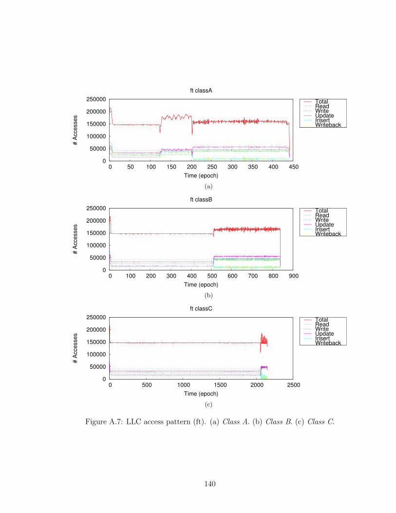
0
50000
100000
150000
200000
250000
0 50 100 150 200 250 300 350 400 450
# A
ccesse
s
Time (epoch)
ft classA
TotalReadWriteUpdateInsertWriteback
(a)
0
50000
100000
150000
200000
250000
0 100 200 300 400 500 600 700 800 900
# A
ccesses
Time (epoch)
ft classB
TotalReadWriteUpdateInsertWriteback
(b)
0
50000
100000
150000
200000
250000
0 500 1000 1500 2000 2500
# A
cce
sses
Time (epoch)
ft classC
TotalReadWriteUpdateInsertWriteback
(c)
Figure A.7: LLC access pattern (ft). (a) Class A. (b) Class B. (c) Class C.
140

0
20000
40000
60000
80000
100000
120000
140000
160000
0 100 200 300 400 500 600
# A
ccesse
s
Time (epoch)
is classA
TotalReadWriteUpdateInsertWriteback
(a)
0
20000
40000
60000
80000
100000
120000
140000
0 100 200 300 400 500 600
# A
ccesses
Time (epoch)
is classB
TotalReadWriteUpdateInsertWriteback
(b)
0
20000
40000
60000
80000
100000
120000
140000
0 100 200 300 400 500 600
# A
cce
sses
Time (epoch)
is classC
TotalReadWriteUpdateInsertWriteback
(c)
Figure A.8: LLC access pattern (is). (a) Class A. (b) Class B. (c) Class C.
141
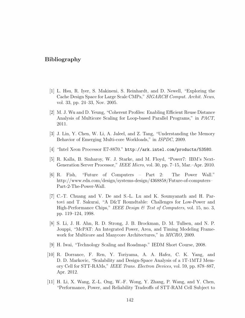
Bibliography
[1] L. Hsu, R. Iyer, S. Makineni, S. Reinhardt, and D. Newell, “Exploring theCache Design Space for Large Scale CMPs,” SIGARCH Comput. Archit. News,vol. 33, pp. 24–33, Nov. 2005.
[2] M. J. Wu and D. Yeung, “Coherent Profiles: Enabling Efficient Reuse DistanceAnalysis of Multicore Scaling for Loop-based Parallel Programs,” in PACT,2011.
[3] J. Lin, Y. Chen, W. Li, A. Jaleel, and Z. Tang, “Understanding the MemoryBehavior of Emerging Multi-core Workloads,” in ISPDC, 2009.
[4] “Intel Xeon Processor E7-8870.” http://ark.intel.com/products/53580.
[5] R. Kalla, B. Sinharoy, W. J. Starke, and M. Floyd, “Power7: IBM’s Next-Generation Server Processor,” IEEE Micro, vol. 30, pp. 7–15, Mar.–Apr. 2010.
[6] R. Fish, “Future of Computers – Part 2: The Power Wall.”http://www.edn.com/design/systems-design/4368858/Future-of-computers–Part-2-The-Power-Wall.
[7] C.-T. Chuang and V. De and S.-L. Lu and K. Soumyanath and H. Par-tovi and T. Sakurai, “A D&T Roundtable: Challenges for Low-Power andHigh-Performance Chips,” IEEE Design & Test of Computers, vol. 15, no. 3,pp. 119–124, 1998.
[8] S. Li, J. H. Ahn, R. D. Strong, J. B. Brockman, D. M. Tullsen, and N. P.Jouppi, “McPAT: An Integrated Power, Area, and Timing Modeling Frame-work for Multicore and Manycore Architectures,” in MICRO, 2009.
[9] H. Iwai, “Technology Scaling and Roadmap.” IEDM Short Course, 2008.
[10] R. Dorrance, F. Ren, Y. Toriyama, A. A. Hafez, C. K. Yang, andD. D. Markovic, “Scalability and Design-Space Analysis of a 1T-1MTJ Mem-ory Cell for STT-RAMs,” IEEE Trans. Electron Devices, vol. 59, pp. 878–887,Apr. 2012.
[11] H. Li, X. Wang, Z.-L. Ong, W.-F. Wong, Y. Zhang, P. Wang, and Y. Chen,“Performance, Power, and Reliability Tradeoffs of STT-RAM Cell Subject to
142

Architecture-Level Requirement,” IEEE Trans. Magnetics, vol. 47, pp. 2356–2359, Oct. 2011.
[12] N. Muralimanohar, R. Balasubramonian, and N. P. Jouppi, “CACTI 6.0: ATool to Model Large Caches,” tech. rep., HP Laboratories, Palo Alto, 2009.
[13] “Predictive Technology Model.” http://ptm.asu.edu/.
[14] X. Dong, C. Xu, Y. Xie, and N. P. Jouppi, “NVSim: A Circuit-Level Per-formance, Energy, and Area Model for Emerging Nonvolatile Memory,” IEEETrans. CAD, vol. 31, pp. 994–1007, July 2012.
[15] A. Patel, F. Afram, S. Chen, and K. K. Ghose, “MARSSx86: A Full SystemSimulator for x86 CPUs,” in DAC, 2011.
[16] C. Bienia, Benchmarking Modern Multiprocessors. PhD thesis, Princeton Uni-versity, Jan. 2011.
[17] “NAS Parallel Benchmarks.” http://www.nas.nasa.gov/Resources/
Software/npb.html.
[18] S. Damaraju, V. George, S. Jahagirdar, T. Khondker, R. Milstrey, S. Sarkar,S. Siers, I. Stolero, and A. Subbiah, “A 22nm IA Multi-CPU and GPU System-on-Chip,” in ISSCC, 2012.
[19] M. Golden, S. Arekapudi, and J. Vinh, “40-Entry Unified Out-of-Order Sched-uler and Integer Execution Unit for the AMD Bulldozer x86-64 Core,” inISSCC, 2011.
[20] J. L. Shin, H. Park, H. Li, A. Smith, Y. Choi, H. Sathianathan, S. Dash,S. Turullols, S. Kim, R. Masleid, G. Konstadinidis, R. Golla, M. J. Doherty,G. Grohoski, and C. McAllister, “The Next-Generation 64b SPARC Core ina T4 SoC Processor,” in ISSCC, 2012.
[21] C. W. Smullen, V. Mohan, A. Nigam, S. Gurumurthi, and M. R. Stan, “Re-laxing Non-Volatility for Fast and Energy-Efficient STT-RAM Caches,” inHPCA, 2011.
[22] Z. Diao, Z. Li, S. Wang, Y. Ding, A. Panchula, E. Chen, L. C. Wang, andY. Huai, “Spin-Transfer Torque Switching in Magnetic Tunnel Junctions andSpin-Transfer Torque Random Access Memory,” J. Physics: Condensed Mat-ter, vol. 19, no. 16, 2007.
[23] A. Jog, A. Mishra, C. Xu, Y. Xie, V. Narayanan, R. Iyer, and C. Das, “CacheRevive: Architecting Volatile STT-RAM Caches for Enhanced Performancein CMPs,” in DAC, 2012.
[24] H. Naeimi, C. Augustine, A. Raychowdhury, S.-L. Lu, and J. Tschanz,“STTRAM Scaling and Retention Failure,” Intel Technology Journal, vol. 17,no. 1, pp. 54–75, 2013.
143

[25] M. Joodaki, Selected Advances in Nanoelectronic Devices: Logic, Memory andRF. Springer, 2013.
[26] N. Butt, K. McStay, A. Cestero, H. Ho, W. Kong, S. Fang, R. Krishnan,B. Khan, A. Tessier, W. Davies, S. Lee, Y. Zhang, J. Johnson, S. Rombawa,R. Takalkar, A. Blauberg, K. V. Hawkins, J. Liu, S. Rosenblatt, P. Goyal,S. Gupta, J. Ervin, Z. Li, S. Galis, J. Barth, M. Yin, T. Weaver, J. H. Li,S. Narasimha, P. Parries, W. K. Henson, N. Robson, T. Kirihata, M. Chudzik,E. Maciejewski, P. Agnello, S. Stiffler, and S. S. Iyer, “A 0.039um2 HighPerformance eDRAM Cell Based on 32nm High-K/Metal SOI Technology,”in IEDM, 2010.
[27] M. Technology, “Micron 8Gb QuadDie DDR3 SDRAM Datasheet,” 2011.
[28] K. C. Chun, P. Jain, J. H. Lee, and C. H. Kim, “A 3T Gain Cell EmbeddedDRAM Utilizing Preferential Boosting for High Density and Low Power On-Die Caches,” IEEE J. Solid-State Circuits, vol. 46, pp. 1495–1505, Jun. 2011.
[29] A. Driskill-Smith, D. Apalkov, V. Nikitin, X. Tang, S. Watts, D. Lottis,K. Moon, A. Khvalkovskiy, R. Kawakami, X. Luo, A. Ong, E. Chen, andM. Krounbi, “Latest Advances and Roadmap for In-Plane and PerpendicularSTT-RAM,” in IMW, 2011.
[30] R. Saleh, “Leakage and Low-Power Design.” http://courses.ece.ubc.ca/
579/579.lect6.leakagepower.08.pdf.
[31] N. Weste and D. Harris, CMOS VLSI Design: A Circuits and Systems Per-spective. Pearson Education, 2004.
[32] W. Regitz and J. Karp, “A Three Transistor-Cell, 1024-bit, 500ns MOSRAM,” in ISSCC, 1970.
[33] T. N. Blalock and R. C. Jaeger, “An Experimental 2T Cell RAM with 7nsAccess Time at Low Temperature,” in Symp. VLSI Circuits, 1990.
[34] N. Ikeda, T. Terano, H. Moriya, T. Emori, and T. Kobayashi, “A Novel LogicCompatible Gain Cell with Two Transistors and One Capacitor,” in Symp.VLSI Technology, 2000.
[35] W. K. Luk and R. H. Dennard, “2T1D Memory Cell with Voltage Gain,” inSymp. VLSI Circuits, 2004.
[36] M. Ichihashi, H. Toda, Y. Itoh, and K. Ishibashi, “0.5V Asymmetric Three-Tr. Cell (ATC) DRAM using 90nm Generic CMOS Logic Process,” in Symp.VLSI Circuits, 2005.
[37] W. K. Luk, J. Cai, R. H. Dennard, M. J. Immediato, and S. V. Kosonocky, “A3-Transistor DRAM Cell with Gated Diode for Enhanced Speed and RetentionTime,” in Symp. VLSI Circuits, 2006.
144

[38] M.-T. Chang, P.-T. Huang, and W. Hwang, “A 65nm Low Power 2T1D Em-bedded DRAM with Leakage Current Reduction,” in SOCC, 2007.
[39] D. Somasekhar, Y. Ye, P. Aseron, S.-L. Lu, M. Khellah, J. Howard, G. Ruhl,T. Karnik, S. Y. Borkar, V. De, and A. Keshavarzi, “2GHz 2Mb 2T Gain-Cell Memory Macro with 128GB/s Bandwidth in a 65nm Logic Process,” inISSCC, 2008.
[40] K. C. Chun, P. Jain, J. H. Lee, and C. H. Kim, “A Sub-0.9V Logic-CompatibleEmbedded DRAM with Boosted 3T Gain Cell, Regulated Bit-Line WriteScheme and PVT-Tracking Read Reference Bias,” in Symp. VLSI Circuits,2009.
[41] K. C. Chun, P. Jain, T. H. Kim, and C. H. Kim, “A 1.1V, 667MHz RandomCycle, Asymmetric 2T Gain Cell Embedded DRAM with a 99.9 percentileretention time of 110u sec,” in Symp. VLSI Circuits, 2010.
[42] Y. Lee, M. T. Chen, J. Park, D. Sylvester, and D. Blaauw, “A 5.42nW/kBRetention Power Logic-Compatible Embedded DRAM with 2T Dual-Vt GainCell for Low Power Sensing Applications,” in ASSCC, 2010.
[43] K. C. Chun, W. Zhang, and P. J. C. H. Kim, “A 700MHz 2T1C Embed-ded DRAM Macro in a Generic Logic Process with no Boosted Supplies,” inISSCC, 2011.
[44] W. Zhang, K. C. Chun, and C. H. Kim, “Variation Aware Performance Anal-ysis of Gain Cell Embedded DRAMs,” in ISLPED, 2010.
[45] C. H. Lin, M. V. Dunga, D. Lu, A. M. Niknejad, and C. Hu, “StatisticalCompact Modeling of Variations in Nano MOSFETs,” in VLSI-TSA, 2008.
[46] J. F. Mesa-Martinez, E. K. Ardestani, and J. Renau, “Characterizing Proces-sor Thermal Behavior,” in ASPLOS, 2010.
[47] “ITRS 2011 Edition.” http://www.itrs.net/Links/2011itrs/home2011.
htm.
[48] A. Driskill-Smith, “Latest Advances and Future Prospects of STT-RAM.”Non-Volatile Memories Workshop, 2010.
[49] T. Wada, S. Rajan, and S. A. Przybylski, “An Analytical Access Time Modelfor On-Chip Cache Memories,” IEEE J. Solid-State Circuits, vol. 27, pp. 1147–1156, Aug. 1992.
[50] J. M. Mulder, N. T. Quach, and M. J. Flynn, “An Area Model for On-ChipMemories and its Application,” IEEE J. Solid-State Circuits, vol. 26, pp. 98–106, Feb. 1991.
145

[51] S. Wilton and N. P. Jouppi, “An Enhanced Access and Cycle Time Model forOn-Chip Caches,” tech. rep., Western Research Laboratory, Palo Alto, 1994.
[52] G. Reinman and N. P. Jouppi, “CACTI 2.0: An Integrated Cache Timing andPower Model,” tech. rep., Western Research Laboratory, Palo Alto, 2000.
[53] P. Shivakumar and N. P. Jouppi, “CACTI 3.0: An Integrated Cache Timing,Power, and Area Model,” tech. rep., Western Research Laboratory, Palo Alto,2001.
[54] M. Mamidipaka and N. Dutt, “eCACTI: An Enhanced Power EstimationModel for On-chip Caches,” tech. rep., CECS, University of California, Irvine.
[55] D. Tarjan, S. Thoziyoor, and N. P. Jouppi, “CACTI 4.0,” tech. rep., HPLaboratories, Palo Alto, 2006.
[56] S. Rodriguez and B. Jacob, “Energy/power breakdown of pipelined nanometercaches (90nm/65nm/45nm/32nm),” in ISLPED, 2006.
[57] S. Thoziyoor, N. Muralimanohar, J. H. Ahn, and N. P. Jouppi, “CACTI 5.1,”tech. rep., HP Laboratories, Palo Alto, 2008.
[58] Y. F. Tsai, Y. Xie, N. Vijaykrishnan, and M. J. Irwin, “Three-DimensionalCache Design Exploration using 3DCacti,” in ICCD, 2005.
[59] V. Mohan, S. Gurumurthi, and M. R. Stan, “FlashPower: A Detailed PowerModel for NAND Flash Memory,” in DATE, 2010.
[60] W. Xu, H. Sun, X. Wang, Y. Chen, and T. Zhang, “Design of Last-Level On-Chip Cache Using Spin-Torque Transfer RAM (STT RAM),” IEEE Trans.VLSI, vol. 19, pp. 483–493, Mar. 2011.
[61] T. Vogelsang, “Understanding the Energy Consumption of Dynamic RandomAccess Memories,” in MICRO, 2010.
[62] C. Y. Lee and N. K. Jha, “CACTI-FinFET: An Integrated Delay and PowerModeling Framework for FinFET-Based Caches under Process Variations,” inDAC, 2011.
[63] S. Li, K. Chen, J. H. Ahn, J. Brockman, and N. P. Jouppi, “CACTI-P: Architecture-Level Modeling for SRAM-Based Structures with AdvancedLeakage Reduction Techniques,” in ICCAD, 2011.
[64] N. P. Jouppi, A. B. Kahng, N. Muralimanohar, and V. Srinivas, “CACTI-IO:CACTI with Off-Chip Power-Area-Timing Models,” in ICCAD, 2012.
[65] A. R. Alameldeen and D. A. Wood, “Variability in Architectural Simulationsof Multi-threaded Workloads,” in HPCA, 2003.
146

[66] J. Hennessy and D. Patterson, Computer Architecture, Fourth Edition: AQuantitative Approach. Morgan Kaufmann Publishers Inc., 2006.
[67] Y. Shao and D. Brooks, “Energy Characterization and Instruction-Level En-ergy Model of Intel’s Xeon Phi Processor,” in ISLPED, 2013.
[68] M. Powell, S. H. Yang, B. Falsafi, K. Roy, and T. N. Vijaykumar, “Gated-Vdd:A Circuit Technique to Reduce Leakage in Deep-Submicron Cache Memories,”in ISLPED, 2000.
[69] B. Amelifard, F. Fallah, and M. Pedram, “Reducing the Sub-threshold andGate-tunneling Leakage of SRAM Cells using Dual-Vt and Dual-Tox Assign-ment,” in DATE, 2006.
[70] C. H. Kim, J. J. Kim, S. Mukhopadhyay, and K. Roy, “A Forward Body-Biased Low-Leakage SRAM Cache: Device and Architecture Considerations,”in ISLPED, 2003.
[71] R. G. Dreslinski, M. Wieckowski, D. Blaauw, D. Sylvester, and T. Mudge,“Near-Threshold Computing: Reclaiming Moore’s Law Through Energy Effi-cient Integrated Circuits,” Proceedings of the IEEE, vol. 98, pp. 253–266, Feb.2010.
[72] R. Pawlowski, E. Krimer, J. Crop, J. Postman, N. Moezzi-Madani, M. Erez,and P. Chiang, “A 530mV 10-Lane SIMD Processor with Variation Resiliencyin 45nm SOI,” in ISSCC, 2012.
[73] D. Fick, R. Dreslinski, B. Giridhar, G. Kim, S. Seo, M. Fojtik, S. Satpathy,Y. Lee, D. Kim, N. Liu, M. Wieckowski, G. Chen, T. Mudge, D. Sylvester,and D. Blaauw, “Centip3De: A 3930DMIPS/W configurable near-threshold3D stacked system with 64 ARM Cortex-M3 cores,” in ISSCC, 2012.
[74] D. H. Albonesi, “Selective Cache Ways: On-Demand Cache Resource Alloca-tion,” in MICRO, 1999.
[75] S. Kaxiras, Z. Hu, and M. Martonosi, “Cache Decay: Exploiting GenerationalBehavior to Reduce Cache Leakage Power,” in ISCA, 2001.
[76] K. Flautner, N. S. Kim, S. Martin, D. Blaauw, and T. Mudge, “DrowsyCaches: Simple Techniques for Reducing Leakage Power,” in ISCA, 2002.
[77] A. Nigam, C. Smullen, V. Mohan, E. Chen, S. Gurumurthi, and M. Stan,“Delivering on the Promise of Universal Memory for Spin-Transfer TorqueRAM (STT-RAM),” in ISLPED, 2011.
[78] P. Zhou, B. Zhao, J. Yang, and Y. Zhang, “Energy Reduction for STT-RAMUsing Early Write Termination,” in ICCAD, 2009.
147

[79] X. Wu, J. Li, L. Zhang, E. Speight, R. Rajamony, and Y. Xie, “Hybrid CacheArchitecture with Disparate Memory Technologies,” in ISCA, 2009.
[80] A. Jadidi, M. Arjomand, and H. Sarbazi-Azad, “High-Endurance andPerformance-Efficient Design of Hybrid Cache Architectures through Adap-tive Line Replacement,” in ISLPED, 2011.
[81] Y. T. Chen, J. Cong, H. Huang, B. Liu, C. Liu, M. Potkonjak, and G. Rein-man, “Dynamically Reconfigurable Hybrid cCache: An Energy-Efficient Last-Level Cache Design,” in DATE, 2012.
[82] Z. Sun, X. Bi, H. Li, W. F. Wong, Z. L. Ong, X. Zhu, and W. Wu, “MultiRetention Level STT-RAM Cache Designs with a Dynamic Refresh Scheme,”in MICRO, 2011.
[83] T. Kirihata, P. Parries, D. R. Hanson, H. Kim, J. Golz, G. Fredeman, R. Ra-jeevakumar, J. Griesemer, N. Robson, A. Cestero, B. A. Khan, G. Wang,M. Wordeman, and S. S. Iyer, “An 800-MHz Embedded DRAM with a Con-current Refresh Mode,” IEEE J. Solid-State Circuits, vol. 40, pp. 1377–1387,Jun. 2005.
[84] T. Ohsawa, K. Kai, and K. Murakami, “Optimizing the DRAM Refresh Countfor Merged DRAM/logic LSIs,” in ISLPED, 1998.
[85] J. Kim and M. C. Papaefthymiou, “Block-Based Multiperiod Dynamic Mem-ory Design for Low Data-Retention Power,” IEEE Trans. VLSI, vol. 11,pp. 1006–1018, Dec. 2003.
[86] J. H. Ahn, B. H. Jeong, S. H. Kim, S. H. Chu, S. K. Cho, H. J. Lee, M. H.Kim, S. I. Park, S. W. Shin, J. H. Lee, B. S. Han, J. . Hong, P. B. Moran, andY. T. Kim, “Adaptive Self Refresh Scheme for Battery Operated High-DensityMobile DRAM Applications,” in ASSCC, 2006.
[87] J. Liu, B. Jaiyen, R. Veras, and O. Mutlu, “RAIDR: Retention-Aware Intel-ligent DRAM Refresh,” in ISCA, 2012.
[88] P. G. Emma, W. R. Reohr, and M. Meterelliyoz, “Rethinking Refresh: In-creasing Availability and Reducing Power in DRAM for Cache Applications,”IEEE Micro, vol. 28, pp. 47–56, Nov.–Dec. 2008.
[89] C. Wilkerson, A. R. Alameldeen, Z. Chishti, W. W. D. Somasekhar, and S.-L. Lu, “Reducing Cache Power with Low-Cost, Multi-Bit Error-CorrectingCodes,” in ISCA, 2010.
[90] W. Yun, K. Kang, and C. M. Kyung, “Thermal-Aware Energy Minimizationof 3D-Stacked L3 Cache with Error Rate Limitation,” in ISCAS, 2011.
[91] W. R. Reohr, “Memories: Exploiting Them and Developing Them,” in SOCC,2006.
148

[92] X. Liang, R. Canal, G. Y. Wei, and D. Brooks, “Process Variation Tolerant3T1D-Based Cache Architectures,” in MICRO, 2007.
[93] M. Ghosh and H. H. Lee, “Smart Refresh: An Enhanced Memory ControllerDesign for Reducing Energy in Conventional and 3D Die-Stacked DRAMs,”in MICRO, 2007.
[94] Z. Hu, S. Kaxiras, and M. Martonosi, “Timekeeping in the Memory System:Predicting and Optimizing Memory Behavior,” in ISCA, 2002.
[95] J. Abella, A. Gonzalez, X. Vera, and M. O’Boyle, “IATAC: A Smart Predictorto Turn-Off L2 Cache Lines,” ACM Trans. Archit. Code Optim., vol. 2, pp. 55–77, Mar. 2005.
[96] H. Zhou, M. Toburen, E. Rotenberg, and T. Conte, “Adaptive Mode Control:A Static-Power-Efficient Cache Design,” in PACT, 2001.
[97] A.-C. Lai and B. Falsafi, “Selective, Accurate, and Timely Self-Invalidationusing Last-Touch Prediction,” in ISCA, 2000.
[98] S. Khan, Y. Tian, and D. Jimenez, “Sampling Dead Block Prediction forLast-Level Caches,” in MICRO, 2010.
[99] Z. Chishti, A. Alameldeen, C. Wilkerson, W. Wu, and S.-L. Lu, “Improvingcache lifetime reliability at ultra-low voltages,” in MICRO, 2009.
[100] F. Bellard, “QEMU, a Fast and Portable Dynamic Translator,” in ATEC,2005.
[101] M. T. Yourst, “PTLsim: A Cycle Accurate Full System x86-64 Microarchitec-tural Simulator,” in ISPASS, 2007.
[102] M.-T. C. I. B. P. E. J. G. Z. C. S.-L. L. J. Stevens, P. Tschirhart and B. Jacob,“An Integrated Simulation Infrastructure for the Entire Memory Hierarchy:Cache, DRAM, Nonvolatile Memory, and Disk,” Intel Technology Journal,vol. 17, no. 1, pp. 184–200, 2013.
[103] H. Al-Zoubi, A. Milenkovic, and M. Milenkovic, “Performance Evaluation ofCache Replacement Policies for the SPEC CPU2000 Benchmark Suite,” inACMSE, 2004.
[104] P. Rosenfeld, E. Cooper-Balis, and B. Jacob, “DRAMSim2: A Cycle AccurateMemory System Simulator,” IEEE Computer Architecture Letters, vol. 10,pp. 16–19, Jan. 2011.
[105] T. Kawahara, “Scalable Spin-Transfer Torque RAM Technology for Normally-Off Computing,” IEEE Design & Test of Computers, vol. 28, pp. 52–63, 2011.
149

[106] W. Kim, J. H. Jeong, Y. Kim, W. C. Lim, J. H. Kim, J. H. Park, H. J.Shin, Y. S. Park, K. S. Kim, S. H. Park, Y. J. Lee, K. W. Kim, H. J. Kwon,H. L. Park, H. S. Ahn, S. C. Oh, J. E. Lee, S. O. Park, S. Choi, H. K. Kang,and C. Chung, “Extended Scalability of Perpendicular STT-MRAM TowardsSub-20nm MTJ Node,” in IEDM, 2011.
[107] J. H. Park, Y. Kim, W. C. Lim, J. H. Kim, S. H. Park, J. H. Kim, W. Kim,K. W. Kim, J. H. Jeong, K. S. Kim, H. Kim, Y. J. Lee, S. C. Oh, J. E.Lee, S. O. Park, S. Watts, D. Apalkov, V. Nikitin, M. Krounbi, S. Jeong,S. Choi, H. K. Kang, and C. Chung, “Enhancement of Data Retention andWrite Current Scaling for Sub-20nm STT-MRAM by Utilizing Dual Interfacesfor Perpendicular Magnetic Anisotropy,” in VLSI Technology, 2011.
[108] M.-T. Chang, P. Rosenfeld, S.-L. Lu, and B. Jacob, “Technology Comparisonfor Large Last-Level Caches (L3Cs): Low-Leakage SRAM, Low Write-EnergySTT-RAM, and Refresh-Optimized eDRAM,” in HPCA, 2013.
[109] A. Keshavarzi, D. Somasekhar, M. Rashed, S. Ahmed, K. Maitra, R. Miller,A. Knorr, J. Cho, R. Augur, S. Banna, C. H. Shaw, A. Halliyal, U. Schroeder,A. Wei, J. Egley, K. Korablev, S. Luning, M. R. Lin, S. Venkatesan, S. Kengeri,and G. Bartlett, “Architecting Advanced Technologies for 14nm and Beyondwith 3D FinFET Transistors for the Future SoC Applications,” in IEDM,2011.
[110] “Intel’s 22nm Tri-Gate Transistors.” http://www.realworldtech.com/
intel-22nm-finfet/.
[111] “Berkeley Short-channel IGFET Model.” http://www-device.eecs.
berkeley.edu/bsim/.
[112] I. Choi and D. Yeung, “Multi-Level Cache Resizing,” tech. rep., UMIACS,University of Maryland, College Park.
150