Embed Size (px)
Citation preview
Ab initio calculations of electron affinity andionization potential of carbon nanotubes
F Buonocore1, F Trani2, D Ninno2, A Di Matteo3, G Cantele4
and G Iadonisi41 STMicroelectronics, Stradale Primosole 50, 95121 Catania, Italy2 Coherentia CNR-INFM, INFN Sezione di Napoli and Universita di Napoli“Federico II”, Dipartimento di Scienze Fisiche, Complesso Universitario Monte S.Angelo, Via Cintia, I-80126 Napoli, Italy.3 STMicroelectronics c/o IMAST P.le Enrico Fermi 1, Localita Granatello PorticiI-80055 Naples, Italy4 Coherentia CNR-INFM and Universita di Napoli “Federico II”, Dipartimento diScienze Fisiche, Complesso Universitario Monte S. Angelo, Via Cintia, I-80126Napoli, Italy.
Abstract. Combining ab initio all-electron and plane wave pseudopotentialcalculations we have studied the electron affinity (EA) and the ionization potential(IP) of (5,5) and (7,0) single wall carbon nanotubes. The role played by finite sizeeffects and nanotube termination have been analyzed comparing hydrogen passivatedand no passivated nanotubes of different lengths. We show that the EA and the IP aredetermined by the interplay between the quantum confinement due to the nanotubefinite length and the charge accumulation on the edges due to its finiteness. The bandstructure, EA and IP of carbon nanotube arrays have also been studied. We show thatin this case the EA and the IP are also controlled by the array density.
PACS numbers: 81.07.De, 31.15.Ar, 73.20.At
E-mail: [email protected]
Submitted to: Nanotechnology

Electron affinity and ionization potential of carbon nanotubes 2
1. Introduction
Interfacing carbon nanotubes either with a metal or with a semiconductor is certainly amost important step in the development of nanoscale electronic devices [1]. Apart fromcertain important aspects related to the formation of dipoles at the interface, it is wellknown that the electronic structure alignment of the two materials near the Fermi levelis largely determined by the mismatch between the Fermi level of the substrate and theelectron affinity/ionization potential of the adsorbed material. These are the drivingconcepts in the design of rectifiers, p-n junctions and transistors [1].
The vast majority of published theoretical works concerning a nanotube surfaceproperty are concentrated on ab initio calculations of the work function (WF). Thedependence of the WF on size, chirality and orientation [2, 3, 4, 5] has been studied.Bundles of nanotubes have also been considered [4, 6]. Apart from differences due todifferent ways of defining the work function and to different computational schemes, thegeneral trend coming from these papers is that, with the exception of small diametertubes, the work function does not dramatically vary upon changing the tube chirality[2] and capping [3]. Strangely enough, the electron affinity (EA) and the ionizationpotential (IP), although related to WF, have not received much attention, neither it hasbeen discussed the interplay between these quantities and the presence of edge localizedstates. It is expected that these states may play an important role in interfacing acarbon nanotube with another material.
The field emission also depends on the EA and IP. In particular, the high aspectratio (height to diameter) of carbon nanotubes makes them an interesting material forrealizing low threshold voltage field emitters. These types of devices include lamps,x-ray tubes and flat panel display. A rich literature has been flourishing in the lastyears on the field emission effect. It is important to note that although early studiesreported field emission where the carbon nanotubes were dispersed in the substrate [7],more recent works achieved an excellent vertical alignment with homogeneous lengthand radius [8]. Moreover, the development of nanopatterning techniques for catalystdeposition, is, in our opinion, opening the way toward the fabrication of nanotubesarrays with a predefined geometry and an intertube distance on the nanometer scalelength. As we shall see in the following, when the intertube distance is of the orderfew A, the interactions between the nanotubes give rise to a band structure whose mainfeatures depend on the nanotube nature (chirality, either open or close edges and soon).
Motivated from the above considerations, in this paper we investigate the electronicproperties of single wall carbon nanotubes with methods rooted on the DensityFunctional Theory. We have analyzed two classes of systems: the isolated nanotube andthe corresponding periodic array. In the first case the emphasis is on the dependence ofEA and IP on both the nanotube type, either armchair or zig-zag, and length. In thesecond case we have analyzed the array band structure and the variations of EA andIP with the intertube distance. In both the cases, some indications are given on the

Electron affinity and ionization potential of carbon nanotubes 3
corresponding work function variations.
2. Computational details
The ab initio calculations have been performed using two different computationalschemes. The first one is an all-electron method as implemented into the DMol3
package (Accelrys Inc.) [9, 10] which uses a localized basis set. As such, the package isparticularly useful in studying confined and isolated systems. The second one is based ona pseudopotential plane wave method as implemented in the QUANTUM-ESPRESSOcode [11]. This code is a good choice for periodic systems such as the nanotube arrays.Our past experience in using such mixed computational schemes is that, provided thesame exchange and correlation functional is used, the numerical convergence has beenreached and a sufficiently large supercell is implemented for the plane wave code, thetwo methods give results in good agreement [12].
All the calculations have been done using the generalized gradient approximation(GGA) with the Perdew, Burke and Ernzerhof (PBE) [13] correlation functional. Forthe all-electron calculations the electronic wave functions are expanded in atom-centeredbasis functions defined on a dense numerical grid. The chosen basis set was the DoubleNumerical plus polarization [14]. This basis is composed of two numerical functions pervalence orbital, supplemented with a polarization function, including, where necessary,a polarization p-function on all the hydrogen atoms. The pseudopotential plane wavecalculations have been performed using ultrasoft pseudopotentials, a 26 Rydberg cut-off for the wavefunctions and a 156 Rydberg cut-off for the charge density. Since thenanotubes considered for the array calculations have a finite length of 8.15 A, we haveused a supercell whose dimension along the nanotube axis has been fixed at 20 A. Wehave checked that this supercell height is sufficient to avoid spurious interactions betweenthe array periodic replicas. We have also verified that a 2 × 2 k-point grid is enough forhaving converged total energies and band structures. For both the calculation schemes,we used a convergence threshold on the force for the geometry optimizations of 0.001Ry/A.
3. Results and discussion
3.1. Isolated Nanotubes
As mentioned before, we have investigated the electronic structure of isolated nanotubewith all-electron calculations. We have focused our attention on two different types ofnanotubes: zig-zag (7,0) and armchair (5,5) nanotubes of different lengths. In both thecases, we have taken the nanotube edges either passivated with hydrogens (H-pass) orallowed the edge carbon atoms to relax without constrictions (no-pass).
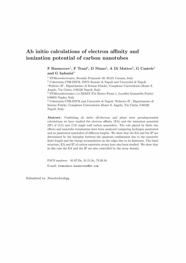
In Fig.1 we plot the electronic orbitals of the H-pass (7,0) nanotube whose energiesare around the HOMO (Highest Occupied Molecular Orbital) and the LUMO (LowestUnoccupied Molecular Orbital). In these calculations the nanotube length has been fixed
Electron affinity and ionization potential of carbon nanotubes 4
Figure 1. (Color online) Molecular orbitals and energy levels of H passivated openedge (7,0) carbon nanotube.
to 23.9 A. It can be seen from this figure that there are four edge localized orbitals, twoHOMOs and two LUMOs which are basically degenerate. The H-pass (5,5), not shownin the figure, has no edge localized orbitals. It is worth mentioning that these resultsare consistent with those of H-pass graphene ribbons. Indeed, in Ref.[15] an analyticexpression for the electronic wave functions of the edge states for graphene ribbonshas been derived in the case of zigzag edges. It has been shown that the nature of thisedge states is topological and, indeed, they were not predicted for armchair structures, inagreement with our findings. As one would expect, the pattern of the edge states changescompletely when the passivating hydrogens are removed. In this case the orbitals of boththe (5,5) and (7,0) nanotubes exhibit edge localized states mainly due to the presenceof dangling bonds. We have found that the no-pass (5,5) nanotube shows delocalizedHOMO and LUMO orbitals, together with four edge localized orbitals very near inenergy, lying at 0.285 eV above the LUMO delocalized orbital. The no-pass (7,0), onthe other hand, has a richer number of localized orbitals, four localized orbitals aboveand two localized orbitals below the HOMO level. We shall see in the following that thiscomplex interplay between edge localized and delocalized orbitals has some influence onboth the EA and IP, and, in the case of a nanotube array, on the band structure.
Electron affinity and ionization potential of carbon nanotubes 5
In Fig.2 we plot the total Mulliken charge computed on atomic planes perpendicularto the nanotube axis. Because of symmetry, the plot is limited to half the distance fromthe nanotube edges. These calculations have been done taking, for each case, nanotubeswith two different lengths. The first observation to be made is that the Mulliken chargenear the nanotube edge has only a very weak dependence on the nanotube length. Thesecond point is that there are significant differences depending on the nanotube typeand the edge termination. The (5,5) H-pass has a dipole near the edge reflecting theability of the hydrogen atom to donate its electron. Because of the armchair shape,the edge carbon atoms tend to form a double bond. In the (5,5) no-pass this dipole isreversed and this is because some electronic charges migrate from the nanotube to theedge. At the same time, the armchair carbon atoms give rise to triple bonds. A goodindication toward this interpretation comes from the calculation of the carbon-carbonbond lengths on the nanotube edge. For the H-pass nanotube we have found a carbon-carbon distance of 1.37 A to be compare with the double bond of C2H4 which we havecalculated to be 1.33 A. For the no-pass nanotube the bond length has been of 1.24A to be compared with that of the triple bond of C2H2 which was 1.20 A. In all theother cases, including the no-pass (7,0) nanotube, the carbon-carbon bond length is inthe range 1.42÷1.44 A being similar to that of graphene. Fig.2 shows that the (7,0)nanotube has a different behavior in the sense that there is no dipole flipping on theedge. This is due to the zig-zag shape of the edge which tend to preserve the graphenebonding pattern. In any case, it should be noted that the removal of the hydrogens fromthe edge does induce a redistribution of charge in the first couple of atomic planes.
For giving a more detailed account of the effects induced by the charge distributionhighlighted by the Mulliken analysis of Fig.2, we show in Fig.3 a 2D contour plot ofthe all-electron electrostatic potential calculated for a (5,5) nanotube considering boththe H-pass and the no-pass edges. At large distance from the nanotube, this potentialdefines the vacuum level so that its distribution around the nanotube cage gives thelocal variations of the work function. The large difference between the two cases isvery evident. In the H-pass nanotube (panel a) the potential raises very rapidly inthe direction orthogonal to the nanotube axis while for the no-pass case the growth israpid on the edges. Another interesting feature is the potential distribution inside thenanotube cage. The hydrogen passivation lowers the potential on the edges whereas thebonding between carbon atoms that occurs when the hydrogens are removed lowers thepotential inside the cage. This findings are fully consistent with the charge distributionsgiven in Fig.2.
The electron affinity is usually defined as EA = E(N + 1) − E(N) where E(N)and E(N + 1) are the total ground-state energies in the neutral (N) and singlycharged (N + 1) configurations. In a similar way, the ionization potential is definedas IP = E(N − 1) − E(N). Although this definition may be very useful for systemssuch as molecules and small nanocrystals, it is better to change it in extended systemsbecause in this case those energy differences are dominated by band structure terms.Once the vacuum level Evac has been determined, EA and IP can be defined starting

Electron affinity and ionization potential of carbon nanotubes 6
Figure 2. Total Mulliken charge calculated on planes perpendicular to the nanotubeaxis. For each nanotube type, the calculation have been done for two different lengthscorresponding to full and open circles.
from the LUMO and HOMO states as EA = Evac − ELUMO and IP = Evac − EHOMO.Assuming a Fermi level sitting in the middle of the gap, the work function is simplygiven by WF = (EA + IP )/2. Although our finite and isolated carbon nanotubes canbe considered as a large molecule, we have preferred to define EA and IP in terms ofLUMO and HOMO states since this choice is consistent with the case of a nanotubearray which will be discussed in the next section. We have seen above that there maybe cases in which the LUMO and the HOMO can either be localized on the nanotubeedges or may be extended over all the structure. It is therefore worth showing what theEA and IP would be when referred to both these states. This will be done for the (7,0)nanotube.
The periodic (5,5) nanotube is a zero gap metal for which we have obtained anall-electron WF of 4.37 eV. The plane wave calculation gives 4.28 eV. For the periodic(7,0) nanotube we have an all-electron WF of 4.82 eV to be compared with the planewave result of 4.75 eV. Although in both the case the two methods are in goodagreement, it should be mentioned that our calculated work functions for the infinitenanotube are smaller than that of ref. [2]. It is possible that the deviations are due

Electron affinity and ionization potential of carbon nanotubes 7
Figure 3. (Color online) Planar contour plots of the all-electron electrostatic potentialof a (5,5) carbon nanotube with (panel a)) and without (panel b)) hydrogen atoms onthe nanotube open edge. The legend is in atomic units and negative values correspondto higher potential.
to the difference between LDA and GGA exchange and correlation functionals. In anycase, the comparison with the many experimental data available is acceptable. TEMmeasurements on multiwall nanotubes give 4.6-4.8 eV [16], photoelectron emission gives4.95 eV and 5.05 eV for multi- and single wall [17], thermionic emission for multi-wallgives 4.54-4.64 eV [18], UPS measurements on single wall gives 4.8 eV [19].
In a finite nanotube, quantum confinement may give a strong dependence of theelectronic properties on the nanotube length. To give a clear insight on this effects, wehave calculated the EA and IP for a number of tubes with increasing length. The resultsare shown in Fig.4 where we show the calculated EA and IP of a (5,5) nanotube with theedges passivated with hydrogens. Both EA and IP, as well as the gap, exhibit regularoscillation on increasing the nanotube length. Despite of this, the quantum confinement

Electron affinity and ionization potential of carbon nanotubes 8
Figure 4. Ionization potential (squares), electron affinity (circles) and work function(triangles) of a H-pass (5,5) nanotube as a function of its length. The inset shows theevolution of the energy gap with the nanotube length.
effects is evidenced by the fact that EA and IP tend, for long nanotube, to approach eachother. This tendency toward metallicity is even more evident looking at the evolutionof the energy gap shown in the inset of Fig.4. The nature of the oscillating energy gapshas been discussed in Ref.[20], where it is shown, with a tight binding calculation, thatinserting the quantum box boundary conditions in the band gap equation determinedby the linear dispersion near the Fermi k-point, the gap of the finite armchair nanotubeis found to vanish every 3 sections (see Ref. [20] for the definition of a section). Ourcalculations shows that the energy gap does not vanish completely and this is becausethe interactions go well beyond the first few nearest-neighbors. An interesting aspect ofthe results shown in Fig.4 is that the work function, defined as WF = (EA + IP )/2,is not influenced by these strong oscillations. Over the explored range of nanotubelengths, WF has an overall variation of about 0.5-0.6 eV. As far as the no-pass (5,5) isconcerned, we have found a similar dependence on the nanotube length of both EA andIP. However, because of the flipping of the nanotube edge dipoles shown in Fig.2, EA,IP and therefore the work function are raised in energy. For instance, for the longestnanotube shown in Fig.4, we have found that EA and IP are raised of 0.6 eV withrespect to those of H-pass nanotubes.
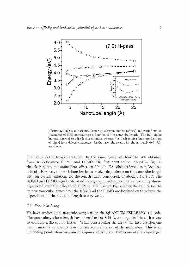
In Fig.5 we show the IP and EA defined either with respect to delocalized HOMOand LUMO (dash joining line) or with respect to the edge localized ones (full joining
Electron affinity and ionization potential of carbon nanotubes 9
Figure 5. Ionization potential (squares), electron affinity (circles) and work function(triangles) of (7,0) nanotube as a function of the nanotube length. The full joiningline are referred to edge localized states whereas the dash joining lines are for dataobtained from delocalized states. In the inset the results for the no passivated (7,0)are shown.
line) for a (7,0) H-pass nanotube. In the same figure we draw the WF obtainedfrom the delocalized HOMO and LUMO. The first point to be noticed in Fig.5 isthe clear quantum confinement effect on IP and EA when referred to delocalizedorbitals. However, the work function has a weaker dependence on the nanotube lengthwith an overall variation, for the length range considered, of about 0.4-0.5 eV. TheHOMO and LUMO edge localized orbitals get approaching each other becoming almostdegenerate with the delocalized HOMO. The inset of Fig.5 shows the results for theno-pass nanotube. Since both the HOMO ad the LUMO are localized on the edges, thedependence on the nanotube length is very weak.
3.2. Nanotube Arrays
We have studied (5,5) nanotube arrays using the QUANTUM-ESPRESSO [11] code.The nanotubes, whose length have been fixed at 8.15 A, are organized in such a wayto compose a 2D square lattice. When constructing the array, the first decision onehas to make is on how to take the relative orientation of the nanotubes. This is aninteresting point whose assessment requires an accurate description of the long-ranged
Electron affinity and ionization potential of carbon nanotubes 10
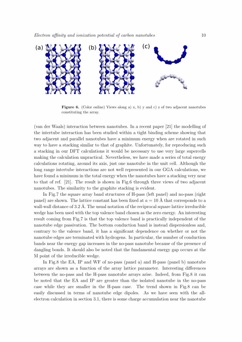
Figure 6. (Color online) Views along a) x, b) y and c) z of two adjacent nanotubesconstituting the array.
(van der Waals) interaction between nanotubes. In a recent paper [21] the modelling ofthe intertube interaction has been studied within a tight binding scheme showing thattwo adjacent and parallel nanotubes have a minimum energy when are rotated in suchway to have a stacking similar to that of graphite. Unfortunately, for reproducing sucha stacking in our DFT calculations it would be necessary to use very large supercellsmaking the calculation unpractical. Nevertheless, we have made a series of total energycalculations rotating, around its axis, just one nanotube in the unit cell. Although thelong range intertube interactions are not well represented in our GGA calculations, wehave found a minimum in the total energy when the nanotubes have a stacking very nearto that of ref. [21]. The result is shown in Fig.6 through three views of two adjacentnanotubes. The similarity to the graphite stacking is evident.
In Fig.7 the square array band structures of H-pass (left panel) and no-pass (rightpanel) are shown. The lattice constant has been fixed at a = 10 A that corresponds to awall-wall distance of 3.2 A. The usual notation of the reciprocal square lattice irreduciblewedge has been used with the top valence band chosen as the zero energy. An interestingresult coming from Fig.7 is that the top valence band is practically independent of thenanotube edge passivation. The bottom conduction band is instead dispersionless and,contrary to the valence band, it has a significant dependence on whether or not thenanotube edges are terminated with hydrogens. In particular, the number of conductionbands near the energy gap increases in the no-pass nanotube because of the presence ofdangling bonds. It should also be noted that the fundamental energy gap occurs at theM point of the irreducible wedge.
In Fig.8 the EA, IP and WF of no-pass (panel a) and H-pass (panel b) nanotubearrays are shown as a function of the array lattice parameter. Interesting differencesbetween the no-pass and the H-pass nanotube arrays arise. Indeed, from Fig.8 it canbe noted that the EA and IP are greater than the isolated nanotube in the no-passcase while they are smaller in the H-pass case. The trend shown in Fig.8 can beeasily discussed in terms of nanotube edge dipoles. As we have seen with the all-electron calculation in section 3.1, there is some charge accumulation near the nanotube

Electron affinity and ionization potential of carbon nanotubes 11
-2
-1
0
1
2
Ene
rgy
(eV
)
Γ ΓX M Y-2
-1
0
1
2
Γ X M Γ Y
Figure 7. Band structures of H-pass (left) and no-pass (right) (5,5) nanotube arrays.The nanotubes have a length of 8.15 A while the array has a lattice constant of 10 A
4
5
6
Ene
rgy
(eV
)
8 10 12 14 16 18 20 22 24 26
a (Å)
3
4
Ene
rgy
(eV
)
(a)
(b)
(a)
(b)
no-pass
H-pass
Figure 8. Ionization potential (squares), electron affinity (circles) and work function(triangles) for no-passivated (panel a) and H-passivated (panel b) (5,5) nanotube array,as a function of the array lattice parameter a. Lines are guides for the eyes.
Electron affinity and ionization potential of carbon nanotubes 12
edge shown by the Mulliken charge of Fig.2. This charge accumulation give rise toedge dipoles that with their orientation control the work function. When an arrayof nanotubes is formed, the surface density of dipole increases on reducing the arraylattice spacing. We therefore have a work function that can either increase or decreaseon reducing the lattice spacing, according to the dipole orientation. This is what Figs.2and 8 show.
4. Conclusion
In this paper (5,5) and (7,0) H-passivated and no-passivated finite size carbon nanotubeshave been studied using ab initio calculations. Taking together all the results we haveobtained, it emerges that the EA and IP in finite carbon nanotubes are controlled bytwo concurrent effects. The first one is similar to a quantum confinement effect in thatit gives a variation of both EA and IP with the nanotube length; the second is a purelyelectrostatic effect due to the formation of edge dipoles. In the case of a nanotube array,the third element that come into play is the array density through which the number ofdipoles per surface area may be varied. Both EA and IP can either increase or decrease(with respect to the isolated nanotube) depending on the dipoles density and orientation.At least in principle, with a nanotechnological control on both the nanotube lengthand array density there are margins for tuning the electron affinity and the ionizationpotential. As a final remark, we would like to mention that in a recent paper [22]the work function of individual single wall carbon nanotubes have been measured withphotoemission microscopy. Analyzing the data coming from a set nanotubes, the authorshave been able to conclude that most of them have work functions whose differencesare within 0.6 eV. Although it may be a fortuitous coincidence, the set of calculationspresented in this work does give an overall work function variations in the range 0.5-0.6eV.
Acknowledgments
This work have been done within the GINT collaboration (Gruppo INFN per leNanoTecnologie). Financial support from the Italian government through the COFIN-PRIN 2005 project is acknowledged. All the calculations have been performed atCINECA-“Progetti Supercalcolo 2007” and “Campus Computational Grid”-Universitadi Napoli “Federico II” advanced computing facilities.
References
[1] Anantram M P and Leonard F 2006 Rep. Prog. Phys. 69 507 and references therein[2] Shan B and Cho K 2005 Phys. Rev. Lett. 94 236602[3] Chen C W and Lee M H 2004 Nanotechnology 15 480[4] Su W S, Leung T C, Li B and Chan C T 2007 Appl. Phys. Lett. 90 163103[5] Agrawal B K, Agrawal S and Srivastava R 2003 J. Phys.: Condens. Matter 15 6931

Electron affinity and ionization potential of carbon nanotubes 13
[6] Reich S, Thomsen C and Ordejon P 2002 Phys. Rev. B 65 155411[7] Wang Q, Setlur A, Lauerhaas J, Dai J, Seelig E and Chang R 1998 Appl. Phys. Lett. 72 2912[8] Li J, Papadopoulos C, Xu J and Moskovits M 1999 Appl. Phys. Lett. 75 367[9] Delley B 1990 J. Chem. Phys. 92 508
[10] Delley B 2000 J. Chem. Phys. 113 7756[11] Baroni S, Corso A D, de Gironcoli S, Giannozzi P, Cavazzoni C, Ballabio G, Scandolo S,
Chiarotti G, Focher P, Pasquarello A, Laasonen K, Trave A, Car R, Marzari N and KokaljA http://www.pwscf.org
[12] Festa G, Cossi M, Barone V, Cantele G, Ninno D and Iadonisi G 2005 J. Chem. Phys. 122 184714[13] Perdew J P, Burke K and Ernzerhof M 1996 Phys. Rev. Lett. 77 3865[14] Andzelm J, King-Smith R D and Fitzgerald G 2001 Chem. Phys. Lett. 335 321[15] Nakada K, Fujita M, Dresselhaus G and Dresselhaus M 1996 Phys. Rev. B 54 17954[16] Gao R, Pan Z and Wang Z L 2001 Appl. Phys. Lett. 78 1757[17] Shiraishi M and Ata M 2001 Carbon 39 1913[18] Liu P, Wei Y, Jiang K, Sun Q, Zhang X, Fan S, Zhang S, Ning C and Deng J 2006 Phys. Rev. B
73 235412[19] Suzuki S, Bower C, Watanabe Y and Zhou O 2000 Appl. Phys. Lett. 76 4007[20] Lu D, Li Y, Rotkin S, Ravaioli U and Schulten K 2004 Nano Lett. 4 2383[21] Carlson A and Dumitrica; T 2007 Nanotechnology 18 065706[22] Saturo Suzuki, Yoshio Watanabe, Yoshikazu Homma, Shin-ya Fukuba, Stefan Heun, Andrea
Locatelli 2004 Appl. Phys. Lett. 85 127