Embed Size (px)
Citation preview

The A4926 is an N-channel power MOSFET driver capable of controlling MOSFETs connected in a half-bridge arrangement and is specifically designed for automotive applications with high-power inductive loads, such as brush DC motors solenoids and actuators.
The A4926 is intended for automotive systems that must meet ASIL requirements. In common with other Allegro A2SIL™ products, this device incorporates features to complement proper system design, allowing users to achieve the required ASIL level.
A unique charge pump regulator provides full gate drive for battery voltages down to 5.5 V for most applications. A bootstrap capacitor is used to provide the above-battery supply voltage required for N-channel MOSFETs.
The half bridge can be controlled by independent logic-level inputs or through the SPI-compatible serial interface. The external power MOSFETs are protected from shoot-through by a programmable dead time.
Integrated diagnostics provide indication of multiple internal faults, system faults, and power bridge faults, and can be configured to protect the power MOSFETs under most short-circuit conditions.
In addition to providing full access to the bridge control, the serial interface is also used to alter programmable settings such as dead time, VDS threshold, and fault blank time. Detailed diagnostic information can be read through the serial interface.
The A4926 is supplied in a 20-lead eTSSOP (suffix LP). This package is lead (Pb) free, with 100% matte-tin leadframe plating (suffix –T).
A4926-DS, Rev. 5MCO-0000155
• Half-bridge MOSFET driver• Bootstrap gate drive for N-channel MOSFET bridge• Cross-conduction protection with adjustable dead time• Charge pump regulator for low supply voltage operation• 5.5 to 50 V supply voltage operating range• SPI-compatible serial interface• Bridge control by direct logic inputs or serial interface• Programmable gate drive• Programmable diagnostics• A2SIL product—device features for
safety-critical systems
Automotive Half-Bridge MOSFET Driver
PACKAGE:
Figure 1: Typical Application
Not to scale
A4926
FEATURES AND BENEFITS DESCRIPTION
February 23, 2022
2
-
20-lead TSSOP with exposed pad (suffix LP)
SPI
A4926
GND
VBAT
ECU Load
• Anti-lock braking systems (ABS)• HVAC (blower fan)• DC pumps (fuel, oil, water)• Solenoids and actuators• Similar industrial applications
APPLICATIONS

Automotive Half-Bridge MOSFET DriverA4926
2Allegro MicroSystems 955 Perimeter Road Manchester, NH 03103-3353 U.S.A.www.allegromicro.com
ABSOLUTE MAXIMUM RATINGS [1]
Characteristic Symbol Notes Rating UnitLoad Supply Voltage VBB –0.3 to 50 V
Regulator Output VREG VREG –0.3 to 16 V
Charge Pump Capacitor Terminal VCP1 CP1 –0.3 to 16 V
Charge Pump Capacitor Terminal VCP2 CP2 VCP1 – 0.3 to VREG + 0.3 V
Battery-Compliant Logic Input Terminals VIB HS, LSn, RESETn, ENABLE –0.3 to 50 V
Logic Input Terminals VI STRn, SCK, SDI –0.3 to 6 V
Logic Output Terminal VO SDO –0.3 to 6 V
Diagnostics Output VDIAG DIAG –0.3 to 50 V
Bridge Drain Monitor Terminal VBRG VBRG –5 to 55 V
Bootstrap Supply Terminal VC C –0.3 to VREG + 50 V
High-Side Gate Drive Output Terminal VGHGH VC – 16 to VC + 0.3 V
GH (transient) –18 to VC + 0.3 V
High-Side Source (Load) Terminal VSS VC – 16 to VC + 0.3 V
S (transient) –18 to VC + 0.3 V
Low-Side Gate Drive Output Terminal VGLGL VREG – 16 to 18 V
GL (transient) –8 to 18 V
Bridge Low-Side Source Terminal VLSSLSS VREG – 16 to 18 V
LSS (transient) –8 to 18 V
Ambient Operating Temperature Range TA Limited by power dissipation –40 to 150 °C
Maximum Continuous Junction Temperature TJ(max) 165 °C
Transient Junction Temperature TJt
Overtemperature event not exceeding 10 seconds, lifetime duration not exceeding 10 hours,guaranteed by design characterization.
180 °C
Storage Temperature Range Tstg –55 to 150 °C
1 With respect to GND. Ratings apply when no other circuit operating constraints are present.
SELECTION GUIDEPart Number Packing Package
A4926KLPTR-T 4000 pieces per reel 6.5 mm × 4.4 mm, 1.2 mm maximum height20-lead TSSOP with exposed thermal pad
THERMAL CHARACTERISTICS: May require derating at maximum conditionsCharacteristic Symbol Test Conditions [2] Value Unit
Package Thermal ResistanceRθJA
4-layer PCB based on JEDEC standard 28 °C/W
2-layer PCB with 3.8 in.2 copper each side 38 °C/W
RθJP 2 °C/W
2 Additional thermal information available on the Allegro website.
SPECIFICATIONS

Automotive Half-Bridge MOSFET DriverA4926
3Allegro MicroSystems 955 Perimeter Road Manchester, NH 03103-3353 U.S.A.www.allegromicro.com
Table of Contents
Features and Benefits 1Description 1Package 1Typical Application 1Selection Guide 2Absolute Maximum Ratings 2Thermal Characteristics 2Pinout Diagram and Terminal List Table 4Functional Block Diagram 5Electrical Characteristics 6
Supply and Reference 6Gate Output Drive 7Logic Inputs and Outputs 8Logic I/O – Dynamic Parameters 8Diagnostics and Protection 9
Timing Diagrams 10Logic Truth Tables 11Functional Description 12
Input and Output Terminal Functions 12Power Supplies 13Pump Regulator 13Gate Drives 13Bootstrap Supply 13Bootstrap Charge Management 13Top-Off Charge Pump 14High-Side Gate Drive 14Low-Side Gate Drive 14
Gate Drive Passive Pull-Down 15Dead Time 15Gate Drive Control 15Logic Control Inputs 16Output Disable 16Sleep Mode 17Diagnostic Monitors 17Status and Diagnostic Registers 17Chip-Level Protection 17Operational Monitors 18Power Bridge and Load Faults 19Fault Action 21Fault Masks 21
Serial Interface 22Configuration Registers 24Diagnostic Registers 24Control Register 24Status Register 25
Serial Register Reference 26Application Information 31
Dead-Time Selection 31Bootstrap Capacitor Selection 31Bootstrap Charging 31VREG Capacitor Selection 32
Input/Output Structures 33Layout Recommendations 34Package Outline Drawing 35

Automotive Half-Bridge MOSFET DriverA4926
4Allegro MicroSystems 955 Perimeter Road Manchester, NH 03103-3353 U.S.A.www.allegromicro.com
Terminal List TableName Number Function
C 15 Bootstrap capacitor
CP1 18 Pump capacitor CCP connection
CP2 17 Pump capacitor CCP connection
DIAG 2 Diagnostic output
ENABLE 3 Gate drive output control input
GH 13 High-side gate drive output
GL 12 Low-side gate drive output
GND 1 Power ground
HS 5 HS control input
LSn 6 LS control input
LSS 11 Low-side source
RESETn 4 Standby mode control input
S 14 Load connection
SCK 8 Serial clock input
SDI 7 Serial data input
SDO 9 Serial data output
STRn 10 Serial strobe (chip select) input
VBB 19 Main power supply
VBRG 20 High-side drain voltage sense
VREG 16 Regulated gate drive supply
PAD – Thermal pad; connect to GND
20-Lead eTSSOP (suffix LP) Pinout Diagram
PINOUT DIAGRAM AND TERMINAL LIST TABLE
PAD
1
2
3
4
5
6
7
8
9
10
20
19
18
17
16
15
14
13
12
11
GND
DIAG
ENABLE
RESETn
HS
LSn
SDI
SCK
SDO
STRn
VBRG
VBB
CP1
CP2
VREG
C
S
GH
GL
LSS

Automotive Half-Bridge MOSFET DriverA4926
5Allegro MicroSystems 955 Perimeter Road Manchester, NH 03103-3353 U.S.A.www.allegromicro.com
Figure 2: Functional Block Diagram
STRn
VBAT
CREG
HS
LSn
DIAG
LSS
GL
GH
S
VBRG
SCKSDI
RESETn
VBB
Logic Supply
Regulator
VDS Monitor
VDS Monitor
LSDrive
ChargePump
Regulator
CCP
CP
1
CP
2
HSDrive
GNDPAD
ENABLE
SDO
VREG
C
Diagnostics & Protection
SerialInterface
Timers
ControlLogic
Charge Pump
Bootstrap Monitor

Automotive Half-Bridge MOSFET DriverA4926
6Allegro MicroSystems 955 Perimeter Road Manchester, NH 03103-3353 U.S.A.www.allegromicro.com
ELECTRICAL CHARACTERISTICS: Valid for TJ = –40 to 150°C, VBB = 5.5 to 50 V, unless otherwise specifiedCharacteristics Symbol Test Conditions Min. Typ. Max. Unit
SUPPLY AND REFERENCE
VBB Functional Operating Range VBB
Operating; outputs active 5.5 – 50 V
Operating; outputs disabled 5 – 50 V
No unsafe states 0 – 50 V
VBB Quiescent CurrentIBBQ
RESETn = high, VBB = 12 V, All gate drive outputs low – 6 20 mA
IBBS RESETn ≤ 300 mV, sleep mode, VBB < 35 V – – 20 µA
Internal Logic Supply Regulator Voltage [3][4] VDL 3.1 3.3 3.5 V
VREG Output Voltage, VRG = 0 VREG
VBB > 7.5 V, IVREG = 0 to 30 mA 7.5 8 8.5 V
6 V < VBB ≤ 7.5 V, IVREG = 0 to 13 mA 7.5 8 8.5 V
5.5 V < VBB ≤ 6 V, IVREG < 8 mA 7.5 8 8.5 V
VREG Output Voltage, VRG = 1 VREG
VBB > 9 V, IVREG = 0 to 30 mA 9 11 11.7 V
7.5 V < VBB ≤ 9 V, IVREG = 0 to 20 mA 9 11 11.7 V
6 V < VBB ≤ 7.5V, IVREG ≤ 0 to 13mA 7.9 – – V
5.5 V < VBB ≤ 6 V, IVREG < 8 mA 7.9 9.5 – V
Bootstrap Diode Forward Voltage VfBOOTID = 10 mA 0.4 0.7 1.0 V
ID = 100 mA 1.2 1.9 2.5 V
Bootstrap Diode Current Limit IDBOOT 250 500 750 mA
Top-Off Charge Pump Current Limit ITOCPM 50 100 – µA
High-Side Gate Drive Static Load Resistance RGSH 250 – – kΩ
System Clock Period tOSC 42.5 50 57.5 ns
Continued on the next page…
Automotive Half-Bridge MOSFET DriverA4926
7Allegro MicroSystems 955 Perimeter Road Manchester, NH 03103-3353 U.S.A.www.allegromicro.com
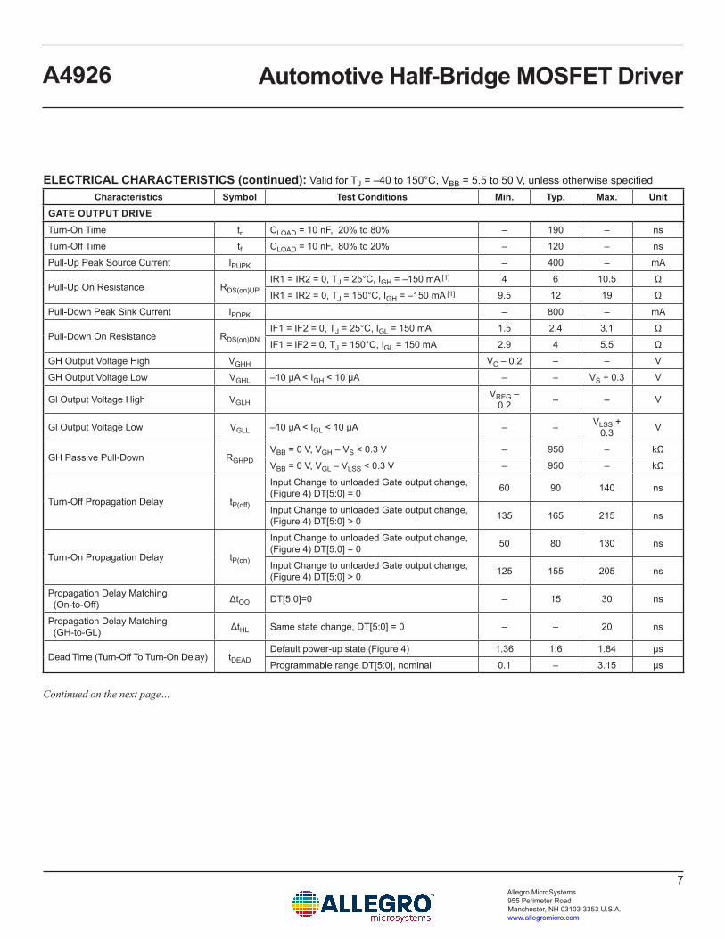
ELECTRICAL CHARACTERISTICS (continued): Valid for TJ = –40 to 150°C, VBB = 5.5 to 50 V, unless otherwise specifiedCharacteristics Symbol Test Conditions Min. Typ. Max. Unit
GATE OUTPUT DRIVETurn-On Time tr CLOAD = 10 nF, 20% to 80% – 190 – ns
Turn-Off Time tf CLOAD = 10 nF, 80% to 20% – 120 – ns
Pull-Up Peak Source Current IPUPK – 400 – mA
Pull-Up On Resistance RDS(on)UPIR1 = IR2 = 0, TJ = 25°C, IGH = –150 mA [1] 4 6 10.5 Ω
IR1 = IR2 = 0, TJ = 150°C, IGH = –150 mA [1] 9.5 12 19 Ω
Pull-Down Peak Sink Current IPDPK – 800 – mA
Pull-Down On Resistance RDS(on)DNIF1 = IF2 = 0, TJ = 25°C, IGL = 150 mA 1.5 2.4 3.1 Ω
IF1 = IF2 = 0, TJ = 150°C, IGL = 150 mA 2.9 4 5.5 Ω
GH Output Voltage High VGHH VC – 0.2 – – V
GH Output Voltage Low VGHL –10 µA < IGH < 10 µA – – VS + 0.3 V
Gl Output Voltage High VGLHVREG –
0.2 – – V
Gl Output Voltage Low VGLL –10 µA < IGL < 10 µA – – VLSS + 0.3 V
GH Passive Pull-Down RGHPDVBB = 0 V, VGH – VS < 0.3 V – 950 – kΩ
VBB = 0 V, VGL – VLSS < 0.3 V – 950 – kΩ
Turn-Off Propagation Delay tP(off)
Input Change to unloaded Gate output change, (Figure 4) DT[5:0] = 0 60 90 140 ns
Input Change to unloaded Gate output change, (Figure 4) DT[5:0] > 0 135 165 215 ns
Turn-On Propagation Delay tP(on)
Input Change to unloaded Gate output change, (Figure 4) DT[5:0] = 0 50 80 130 ns
Input Change to unloaded Gate output change, (Figure 4) DT[5:0] > 0 125 155 205 ns
Propagation Delay Matching (On-to-Off) ΔtOO DT[5:0]=0 – 15 30 ns
Propagation Delay Matching (GH-to-GL) ΔtHL Same state change, DT[5:0] = 0 – – 20 ns
Dead Time (Turn-Off To Turn-On Delay) tDEADDefault power-up state (Figure 4) 1.36 1.6 1.84 µs
Programmable range DT[5:0], nominal 0.1 – 3.15 µs
Continued on the next page…

Automotive Half-Bridge MOSFET DriverA4926
8Allegro MicroSystems 955 Perimeter Road Manchester, NH 03103-3353 U.S.A.www.allegromicro.com
ELECTRICAL CHARACTERISTICS (continued): Valid for TJ = –40 to 150°C, VBB = 5.5 to 50 V, unless otherwise specifiedCharacteristics Symbol Test Conditions Min. Typ. Max. Unit
LOGIC INPUT AND OUTPUTSInput Low Voltage VIL – – 0.8 V
Input High Voltage VIH All logic inputs 2.0 – – V
Input Hysteresis VIhys RESETn inputs 200 400 – mV
Input Hysteresis VIhys All other logic inputs 250 550 – mV
Input Pull-Down HS, ENABLE, RESETn
RPD 0 < VIN < 3 V – 50 – kΩ
IPD 3 V < VIN < 50 V – 70 – µA
Input Pull-Down SDI, SCK RPDS 0 < VIN < 3 V – 50 – kΩ
Input Pull-Up Current to VDL IPU STRn – 70 – µA
Input Pull-Up to VDL RPU LSn – 170 – kΩ
Output Low Voltage SDO, DIAG VOL IOL = 1 mA – 0.1 0.4 V
Output High Voltage SDO VOHSIOS = –200 µA [1] VDL – 0.1 – – V
IOS = –1 mA [1] VDL – 0.4 – – V
Output Leakage SDO [1] IOS 0 V < VOS < VDL, STRn = 1 –1 – 1 µA
Output Current Limit (DIAG) IOLDLIM0 V < VOD < 12 V, DIAG active – 10 17 mA
18 V ≤ VOD < 50 V, DIAG active – – 2.5 mA
Output Leakage [1] (DIAG) IOD0 V < VOD < 12 V, DIAG inactive –1 – 1 µA
18 V ≤ VOD < 50 V, DIAG inactive – – 2.5 mA
LOGIC I/O – DYNAMIC PARAMETERSReset Pulse Width tRST 0.5 – 4.5 µs
Reset Shutdown Time tRSD 30 – – µs
Input Pulse Filter Time tPIN HS, LSn – 35 – ns
Clock High Time tSCKH A in Figure 3 50 – – ns
Clock Low Time tSCKL B in Figure 3 50 – – ns
Strobe Lead Time tSTLD C in Figure 3 30 – – ns
Strobe Lag Time tSTLG D in Figure 3 30 – – ns
Strobe High Time tSTRH E in Figure 3 300 – – ns
Data Out Enable Time tSDOE F in Figure 3 – – 40 ns
Data Out Disable Time tSDOD G in Figure 3 – – 30 ns
Data Out Valid Time From Clock Falling tSDOV H in Figure 3 – – 40 ns
Data Out Hold Time From Clock Falling tSDOH I in Figure 3 5 – – ns
Data In Set-Up Time To Clock Rising tSDIS J in Figure 3 15 – – ns
Data In Hold Time From Clock Rising tSDIH K in Figure 3 10 – – ns
Wake Up From Sleep tEN – – 2 ms
Continued on the next page…
Automotive Half-Bridge MOSFET DriverA4926
9Allegro MicroSystems 955 Perimeter Road Manchester, NH 03103-3353 U.S.A.www.allegromicro.com
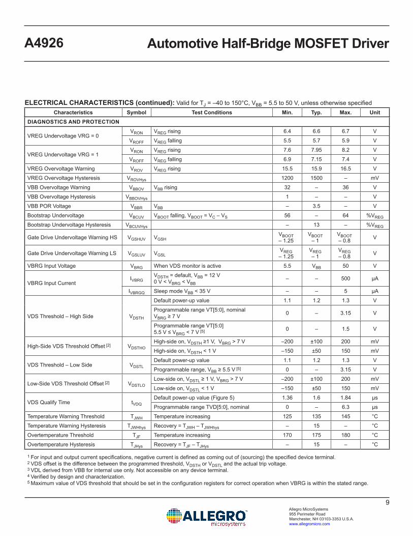
ELECTRICAL CHARACTERISTICS (continued): Valid for TJ = –40 to 150°C, VBB = 5.5 to 50 V, unless otherwise specifiedCharacteristics Symbol Test Conditions Min. Typ. Max. Unit
DIAGNOSTICS AND PROTECTION
VREG Undervoltage VRG = 0VRON VREG rising 6.4 6.6 6.7 V
VROFF VREG falling 5.5 5.7 5.9 V
VREG Undervoltage VRG = 1VRON VREG rising 7.6 7.95 8.2 V
VROFF VREG falling 6.9 7.15 7.4 V
VREG Overvoltage Warning VROV VREG rising 15.5 15.9 16.5 V
VREG Overvoltage Hysteresis VROVHys 1200 1500 – mV
VBB Overvoltage Warning VBBOV VBB rising 32 – 36 V
VBB Overvoltage Hysteresis VBBOVHys 1 – – V
VBB POR Voltage VBBR VBB – 3.5 – V
Bootstrap Undervoltage VBCUV VBOOT falling, VBOOT = VC – VS 56 – 64 %VREG
Bootstrap Undervoltage Hysteresis VBCUVHys – 13 – %VREG
Gate Drive Undervoltage Warning HS VGSHUV VGSH VBOOT – 1.25
VBOOT – 1
VBOOT – 0.8 V
Gate Drive Undervoltage Warning LS VGSLUV VGSL VREG – 1.25
VREG – 1
VREG – 0.8 V
VBRG Input Voltage VBRG When VDS monitor is active 5.5 VBB 50 V
VBRG Input CurrentIVBRG
VDSTH = default, VBB = 12 V0 V < VBRG < VBB
– – 500 µA
IVBRGQ Sleep mode VBB < 35 V – – 5 µA
VDS Threshold – High Side VDSTH
Default power-up value 1.1 1.2 1.3 V
Programmable range VT[5:0], nominalVBRG ≥ 7 V 0 – 3.15 V
Programmable range VT[5:0]5.5 V ≤ VBRG < 7 V [5] 0 – 1.5 V
High-Side VDS Threshold Offset [2] VDSTHOHigh-side on, VDSTH ≥1 V, VBRG > 7 V –200 ±100 200 mV
High-side on, VDSTH < 1 V –150 ±50 150 mV
VDS Threshold – Low Side VDSTLDefault power-up value 1.1 1.2 1.3 V
Programmable range, VBB ≥ 5.5 V [5] 0 – 3.15 V
Low-Side VDS Threshold Offset [2] VDSTLOLow-side on, VDSTL ≥ 1 V, VBRG > 7 V –200 ±100 200 mV
Low-side on, VDSTL < 1 V –150 ±50 150 mV
VDS Qualify Time tVDQDefault power-up value (Figure 5) 1.36 1.6 1.84 µs
Programmable range TVD[5:0], nominal 0 – 6.3 µs
Temperature Warning Threshold TJWH Temperature increasing 125 135 145 °C
Temperature Warning Hysteresis TJWHhys Recovery = TJWH – TJWHhys – 15 – °C
Overtemperature Threshold TJF Temperature increasing 170 175 180 °C
Overtemperature Hysteresis TJHys Recovery = TJF – TJHys – 15 – °C
1 For input and output current specifications, negative current is defined as coming out of (sourcing) the specified device terminal.2 VDS offset is the difference between the programmed threshold, VDSTH or VDSTL and the actual trip voltage.3 VDL derived from VBB for internal use only. Not accessible on any device terminal.4 Verified by design and characterization.5 Maximum value of VDS threshold that should be set in the configuration registers for correct operation when VBRG is within the stated range.

Automotive Half-Bridge MOSFET DriverA4926
10Allegro MicroSystems 955 Perimeter Road Manchester, NH 03103-3353 U.S.A.www.allegromicro.com
XXXX X
C A B D E
J K
F I G
D15 D14 D0
D15’ D14’ D0’
STRn
SCK
SDI
SDO
H
Z Z
HS
LSn
GH
GL
tDEAD
tDEADtP(off)
tP(off) tP(on) tP(off)
tP(on) tP(off)Synchronous Rectification High-side pwm Low-side pwm
Gx
VDS
Fault Bit
MOSFET turn onFault present
MOSFET onTransient disturbanceNo fault present
MOSFET onFault occurs
MOSFET turn onNo fault present
tVDQtVDQ
MOSFET turn onNo fault present
MOSFET turn onFault present
MOSFET onTransient disturbanceNo fault present
MOSFET onFault occurs
Gx
VDS
Fault Bit
tVDQ tVDQtVDQ tVDQ
Figure 3: Serial Interface Timing (X = don’t care, Z = high impedance (tri-state))
Figure 4: Gate Drive Timing – Control Inputs
Figure 5a: VDS Fault Monitor – Blank Mode Timing (VDQ = 1)
Figure 5b: VDS Fault Monitor – Debounce Mode Timing (VDQ = 0)

Automotive Half-Bridge MOSFET DriverA4926
11Allegro MicroSystems 955 Perimeter Road Manchester, NH 03103-3353 U.S.A.www.allegromicro.com
LOGIC TRUTH TABLES
Table 1: Control Logic (Control by Logic Inputs)HS LSn GH GL S0 1 LO LO Z
0 0 LO HI LO
1 1 HI LO HI
1 0 LO LO Z
HI = high-side FET active, LO = low-side FET activeZ = high impedance, both FETs offAll control register bits set to 0, RESETn = 1, ENABLE = 1
Internal control signals (HI, LO) are derived by combining the logic states applied to the control input terminals (HS, LS) with the bit patterns held in the Control register (HSR, LSR).
Normally the input terminals or the Control register method is used for control with the other being held inactive (all termials or bits at logic 0).
Table 2: Control Logic (Control by Serial Register)HSR LSR GH GL S
0 0 LO LO Z
0 1 LO HI LO
1 0 HI LO HI
1 1 LO LO Z
HI = high-side FET active, LO = low-side FET activeZ = high impedance, both FETs offHS = 0, LSN = 1, RESETn = 1, ENABLE = 1
Table 3: Control combination logic table – Logic Inputs and Serial RegisterTerminal Register Internal Terminal Register Internal
HS HSR HI LSn LSR LO0 0 0 0 0 1
0 1 1 0 1 1
1 0 1 1 0 0
1 1 1 1 1 1
ENABLE HI LO GH GL S Comment1 0 0 L L Z Bridge disabled
1 0 1 L H LO Bridge sinking
1 1 0 H L HI Bridge sourcing
1 1 1 L L Z Bridge disabled
0 X X L L Z Bridge disabled
X = don’t care

Automotive Half-Bridge MOSFET DriverA4926
12Allegro MicroSystems 955 Perimeter Road Manchester, NH 03103-3353 U.S.A.www.allegromicro.com
FUNCTIONAL DESCRIPTION
The A4926 is a half-bridge (H-bridge) MOSFET driver (pre-driver) requiring a single unregulated supply of 5.5 to 50 V. It includes an integrated linear regulator to supply the internal logic. All logic inputs are TTL compatible and can be driven by 3.3 or 5 V logic.
The two high-current gate drives are capable of driving a wide range of N-channel power MOSFETs, and are configured as a half-bridge driver with one high-side drive and one low-side drive. The A4926 provides all necessary circuits to ensure that the gate-source voltage of both high-side and low-side external FETs are above 10 V, at supply voltages down to 7 V. For extreme battery voltage drop conditions, correct functional operation is guaranteed at supply voltages down to 5.5 V, but with a reduced gate drive voltage.
Gate drives can be controlled directly through the logic input ter-minals or through an SPI-compatible serial interface. The sense of the logic inputs are arranged to allow the bridge to be driven by a single PWM input if required. The bridge can also be driven by direct logic inputs or by two PWM signals depending on the required complexity. The logic inputs are battery voltage compli-ant, meaning they can be shorted to ground or supply without damage, up to the maximum battery voltage of 50 V.
Bridge efficiency can be enhanced by using the synchronous rectification ability of the drives. When synchronous rectification is used, cross-conduction (shoot through) in the external bridge is avoided by an adjustable dead time. A hardwired logic lockout ensures that the high-side and the low-side cannot be permanently active at the same time.
A low-power sleep mode allows the A4926, the power bridge, and the load to remain connected to a vehicle battery supply with-out the need for an additional supply switch.
The A4926 includes a number of diagnostic features to provide indication and/or protection against undervoltage, overtempera-ture, and power bridge faults. A single diagnostic output provides basic fault indication and detailed diagnostic information is available through the serial interface. The serial interface also provides access to programmable dead time, fault blanking time and programmable VDS threshold for short detection.
Input and Output Terminal FunctionsVBB: Main power supply for internal regulators and charge pump. The main power supply should be connected to VBB through a reverse voltage protection circuit and should be decoupled with ceramic capacitors connected close to the supply and ground terminals.
VBRG: Sense input to the top of the external MOSFET bridge. Allows accurate measurement of the voltage at the drain of the high-side MOSFET in the bridge.
CP1, CP2: Pump capacitor connection for charge pump. Con-nect a minimum 220 nF, typically 470 nF, ceramic capacitor between CP1 and CP2.
VREG: programmable regulated voltage, 8 or 11 V, used to sup-ply the low-side gate drivers and to provide current for the above supply charge pump. A sufficiently large storage capacitor must be connected to this terminal to provide the required transient charging current.
GND: Analog, digital, and power ground. Connect to supply ground–see Layout Recommendations.
C: High-side connection for the bootstrap capacitor and positive supply for the high-side gate driver.
GH: High-side, gate-drive output for an external N-channel MOSFET.
S: Source connection for high-side MOSFET providing the nega-tive supply connections for the floating high-side driver.
GL: Low-side gate-drive output for an external N-channel MOS-FET.
LSS: Low-side return path for discharge of the capacitance on the low-side MOSFET gate, connected to the source of the low-side external MOSFET independently through a low-impedance track.
HS: Logic inputs with pull-down to control the high-side gate drive. Battery voltage compliant terminal.
LSn: Logic input with pull-up to control the low-side gate drive. This is an active-low input. Battery voltage compliant terminal.
ENABLE: Logic input to enable the gate drive outputs. Battery voltage compliant terminal.

Automotive Half-Bridge MOSFET DriverA4926
13Allegro MicroSystems 955 Perimeter Road Manchester, NH 03103-3353 U.S.A.www.allegromicro.com
RESETn: Clears latched faults that may have disabled the out-puts when taken low for the reset pulse width, tRST. Forces low-power shutdown (sleep) when held low for more than the RESET shutdown time, tRSD. Battery voltage compliant terminal.
SDI: Serial data logic input with pull-down. 16-bit serial word input msb first.
SDO: Serial data output. High impedance when STRn is high. Outputs bit 15 of the diagnostic register, the fault flag, as soon as STRn goes low.
SCK: Serial clock logic input with pull-down. Data is latched in from SDI on the rising edge of SCK. There must be 16 rising edges per write and SCK must be held high when STRn changes.
STRn: Serial data strobe and serial access enable logic input with pull-up. When STRn is high, any activity on SCK or SDI is ignored and SDO is high impedance, allowing multiple SDI slaves to have common SDI, SCK, and SDO connections.
DIAG: Diagnostic output. Provides general fault flag output.
Power SuppliesA single power supply voltage is required. The main power sup-ply, VBB, should be connected to VBB through a reverse voltage protection circuit. A 100 nF ceramic decoupling capacitor must be connected close to the supply and ground terminals.
An internal regulator provides the supply to the internal logic. All logic is guaranteed to operate correctly to below the regula-tor undervoltage levels ensuring that the A4926 will continue to operate safely until all logic is reset when a power-on-reset state is present.
The A4926 will operate within specified parameters with VBB from 7 to 50 V and will function correctly with a supply down to 5.5 V. This provides a rugged solution for use in the harsh auto-motive environment.
Pump RegulatorThe gate drivers are powered by a programmable voltage internal regulator which limits the supply to the drivers and therefore the maximum gate voltage. At low supply voltage, the regulated supply is maintained by a charge pump boost converter which requires a pump capacitor, typically 470 nF, connected between the CP1 and CP2 terminals.
The regulated voltage, VREG, can be programmed to 8 or 11 V and is available on the VREG terminal. The voltage level is selected by the value of the VRG bit. When VRG = 1, the voltage
is set to 11 V; when VRG = 0 the voltage is set to 8 V. A suf-ficiently large storage capacitor (see Application Information section) must be connected to this terminal to provide the tran-sient charging current to the low-side drivers and the bootstrap capacitors.
Gate DrivesThe A4926 is designed to drive external, low on-resistance, power N-channel MOSFETs. It will supply the large transient currents necessary to quickly charge and discharge the external MOSFET gate capacitance in order to reduce dissipation in the external MOSFET during switching. The charge current for the low-side drive is provided by the capacitor on the VREG termi-nal. The charge current for the high-side drives is provided by the bootstrap capacitor connected between the C and S terminals. MOSFET gate charge and discharge rates may be controlled by setting a group of parameters via the serial interface or by using an external gate resistor between the gate drive output and the gate terminal of the MOSFET.
Bootstrap SupplyWhen the high-side drivers are active, the reference voltage for the driver will rise to close to the bridge supply voltage. The supply to the driver will then have to be above the bridge supply voltage to ensure that the driver remains active. This temporary high-side supply is provided by a bootstrap capacitor connected between the bootstrap supply terminal, C, and the high-side refer-ence terminal, S.
The bootstrap capacitor is independently charged to approxi-mately VREG when the associated reference S terminal is low. When the output swings high, the voltage on the bootstrap supply terminal rises with the output to provide the boosted gate voltage needed for the high-side N-channel power MOSFETs.
Bootstrap Charge ManagementThe A4926 monitors the bootstrap capacitor charge voltage to ensure sufficient high-side drive. It also includes an optional bootstrap capacitor charge management system (bootstrap man-ager) to ensure that the bootstrap capacitor remains sufficiently charged under all conditions. The bootstrap manager is enabled by default but may be disabled by setting the DBM bit to 1. This may be required in systems where the output MOSFET switching must only be allowed by the controlling processor.
Before a high-side drive can be turned on, the bootstrap capacitor voltage must be higher than the turn-on voltage threshold, VBCUV + VBCUVHys. If this is not the case, then the A4926 will attempt

Automotive Half-Bridge MOSFET DriverA4926
14Allegro MicroSystems 955 Perimeter Road Manchester, NH 03103-3353 U.S.A.www.allegromicro.com
to charge the bootstrap capacitor by activating the low-side drive. Under normal circumstances this will charge the capacitor above the turn-on voltage in a few microseconds and the high-side drive will then be enabled. The bootstrap voltage monitor remains active while the high-side drive is active and if the voltage drops below the turn-off voltage threshold, VBCUV, a charge cycle is also initiated.
The bootstrap charge management circuit may actively charge the bootstrap capacitor regularly when the PWM duty cycle is very high, particularly when the PWM off-time is too short to permit the bootstrap capacitor to become sufficiently charged.
In some systems, it may not be desirable to permit this feature. In this case the bootstrap manager may be disabled by setting the DBM bit to 1. If the bootstrap manager is disabled, then the user must ensure that the bootstrap capacitor does not become discharged below the bootstrap undervoltage threshold, VBCUV, or a bootstrap fault will be indicated and the outputs disabled. This can happen with very high PWM duty cycles when the charge time for the bootstrap capacitor is insufficient to ensure a sufficient recharge to match the MOSFET gate charge transfer during turn on.
If, for any reason, the bootstrap capacitor cannot be sufficiently charged a bootstrap fault will occur—see diagnostics section for further details.
Top-Off Charge PumpAn additional “top-off” charge pump is provided, which will allow the high-side drive to maintain the gate voltage on the external MOSFET indefinitely, ensuring so-called 100% PWM if required. This is a low-current trickle charge pump and is only operated after a high side has been signaled to turn on. There is a small amount of bias current drawn from the C terminal to oper-ate the floating high side circuit (<40 µA) and the charge pump simply provides enough drive to ensure the bootstrap voltage, and hence the gate voltage, will not droop due to this bias current.
In some applications, a safety resistor is added between the gate and source of each MOSFET in the bridge. When a high-side MOSFET is held in the on state, the current through the associ-ated high-side gate-source resistor (RGSH) is provided by the high-side driver and therefore appears as a static resistive load on the top-off charge pump. The minimum value of RGSH for which the top-off charge pump can provide current, without dropping below the bootstrap undervoltage threshold, is defined in the Electrical Characteristics table.
In all cases, the charge required for initial turn-on of the high-side gate is always supplied by the bootstrap capacitor. If the bootstrap capacitor becomes discharged, the top-off charge pump alone will not provide sufficient current to allow the MOSFET to turn on.
High-Side Gate DriveA high-side gate-drive output for an external N-channel MOS-FETs is provided on the GH terminal. GH = 1 (or “high”) means that the upper-half of the driver is turned on and its drain will source current to the gate of the high-side MOSFET in the exter-nal load-driving bridge, turning it on. GH = 0 (or “low”) means that the lower-half of the driver is turned on and its drain will sink current from the external MOSFET’s gate circuit to the S terminal, turning it off.
The reference point for the high-side drive is the load connec-tions, S. This terminal senses the voltage at the load connections. This terminal is also connected to the negative side of the boot-strap capacitor and is the negative supply reference connections for the floating high-side driver. The discharge current from the high-side MOSFET gate capacitance flows through these connec-tions which should have low-impedance traces to the MOSFET bridge.
Low-Side Gate DriveThe low-side gate-drive output on GL is referenced to the LSS terminal. This output is designed to drive an external N-channel power MOSFET. GL = 1 (or “high”) means that the upper-half of the driver is turned on and its drain will source current to the gate of the low-side MOSFET in the external power bridge, turning it on. GL = 0 (or “low”) means that the lower-half of the driver is turned on and its drain will sink current from the external MOS-FET’s gate circuit to the LSS terminal, turning it off.
The LSS terminal provides the return path for discharge of the capacitance on the low-side MOSFET gate. This terminal is connected independently to the source of the low-side external MOSFETs through a low-impedance track.
An integrated slew control feature allows the MOSFET gate charge and discharge rates to be controlled via the serial interface as detailed in the Gate Drive Control section.
Either the internal slew control or an external resistor between the gate drive output and the gate connection to the MOSFET (as close as possible to the MOSFET) can be used to control the slew rate seen at the gate, thereby controlling the di/dt and dv/dt of the voltage at the S terminal.

Automotive Half-Bridge MOSFET DriverA4926
15Allegro MicroSystems 955 Perimeter Road Manchester, NH 03103-3353 U.S.A.www.allegromicro.com
Gate Drive Passive Pull-DownEach gate drive output includes a discharge circuit to ensure that any external MOSFET connected to the gate drive output is held off when the power is removed. This discharge circuit appears as 950 kΩ between the gate drive and the source connec-tions for each MOSFET. It is only active when the A4926 is not driving the output to ensure that any charge accumulated on the MOSFET gate has a discharge path even when the power is not connected.
Dead TimeTo prevent cross-conduction (shoot through) of the power MOS-FET bridge, it is necessary to have a dead-time delay between a high- or low-side turn-off and the next turn-on event. The poten-tial for cross-conduction occurs when the high-side and low-side pair of MOSFETs is switched at the same time, for example, at the PWM switch point. In the A4926, the dead time is set by the contents of the DT[5:0] bits in configuration register 0. These six bits contain a positive integer that determines the dead time by division from the system clock.
The dead time is defined as:
tDEAD = n × 50 nswhere n is a positive integer defined by DT[5:0] and
tDEAD has a minimum active value of 100 ns.
The accuracy of tDEAD is determined by the accuracy of the system clock as defined in the electrical characteristics table. The range of it is 100 ns to 3.15 µs. A value of 1 or 2 in DT[5:0] will set the minimum active dead time of 100 ns.
If DT[5:0] is left at the default value of zero, the dead timer is disabled and no minimum dead time is generated by the A4926. The logic that prevents permanent cross-conduction is, however, still active. Adequate dead time must be generated externally by, for example, the microcontroller producing the drive signals applied to the A4926 logic inputs or Control register.
The internally generated dead time is only present if the on com-mand for one MOSFET occurs within one dead time after the off command for the complimentary MOSFET. In the case where one side of the drive is permanently off the dead time will not occur. In this case the gate drive will turn on within the specified propagation delay after the input goes high. (see Figure 4).
Gate Drive Control MOSFET gate drives are controlled according to the values set in Config 6, 7, and 8 registers.
t1
Gate Drive Command
State
VDS
VGSMiller Region
I1OFF I2 ON
Figure 6a: Off-to-On Transition (Gate Drive)
OFF ON
Gate Drive Command
State
VGS
VDS
Miller Region
Figure 6b: Off-to-On Transition (Switched)
I1ON OFF
Gate Drive Command
State
VGS
VDS
I2
t1
Miller Region
Figure 6c: On-to-Off Transition (Gate Drive)
Gate Drive Command
ON OFFState
VGS
VDS
Miller Region
Figure 6d: On-to-Off Transition (Switched)

Automotive Half-Bridge MOSFET DriverA4926
16Allegro MicroSystems 955 Perimeter Road Manchester, NH 03103-3353 U.S.A.www.allegromicro.com
MOSFET off-to-on transitions are controlled as detailed in Figure 6a. When a gate drive is commanded to turn on a current, I1 (as defined by IR1[3:0]), is sourced on the GH or GL terminal for a duration, t1 (defined by TR[3:0]). These parameters should typi-cally be set so as to quickly charge the MOSFET input capaci-tance to the start of the Miller region as drain-source voltage does not change during this period. Thereafter, the current sourced on GH or GL is set to a value of I2 (as defined by IR2[3:0]) and remains at this value while the MOSFET transitions through the Miller region, and reaches the fully on state. For the high-side MOSFET, fully on is assumed when the drain-source voltage, VDS = VBRG – VS, < VDSTH. For the low-side MOSFET, fully on is assumed when VDS = VS – VLSS, < VDSTL.
I2 should be set to achieve the required input capacitance charge time. Once in the fully on state, the GH or GL output switches from current to voltage drive to hold the MOSFET in the on state.
If the values of IR1[3:0] and IR2[3:0] are set to 0, GH or GL produces maximum drive to turn on the MOSFET as quickly as possible without attempting to control the MOSFET input capaci-tance charge time (Figure 6b). The value of TR[3:0] has no effect on switching speed.
MOSFET on-to-off transitions are controlled as detailed in Figure 6c. When a gate drive is commanded to turn off, a current, I1 (as defined by IF1[3:0]), is sunk by the GH or GL terminal for a duration, t1 (defined by TF[3:0]). These parameters should typically be set so as to quickly discharge the MOSFET input capacitance to the start of the Miller region as drain-source volt-age does not change during this period. Thereafter, the current sunk by GH or GL is set to a value of I2 (as defined by IF2[3:0]) and remains at this value while the MOSFET transitions through the Miller region and reaches the fully off state. For the high-side MOSFET, fully off is assumed when VDS(low side) = VS – VLSS < VDSTH. For the low-side MOSFET, fully off is assumed when VDS(high side) = VBRG – VS < VDSTH. I2 should be set to achieve the required MOSFET input capacitance discharge time. Once in the fully off condition, the GH or GL output switches from cur-rent to voltage drive to hold the MOSFET in the off state.
If the values of IF1[3:0] and IF2[3:0] are set to 0, GH or GL produces maximum drive to turn off the MOSFET as quickly as possible without attempting to control the MOSFET input capacitance discharge time (Figure 6d). The value of TF[3:0] has no effect on switching speed.
Dead time, DT[5:0] in the Config 0 register, must be set to a non-zero value for gate drive control to be operational. Otherwise, maximum drive will be produced on all switching transitions to minimize MOSFET switching times.
Logic Control InputsTwo logic level digital inputs provide direct control for the gate drives, one for each drive. These TTL threshold logic inputs can be driven from 3.3 or 5 V logic and all have a typical hysteresis of 500 mV to improve noise performance. Each input can be shorted to the VBB supply, up to the absolute maximum supply voltage, without damage to the input.
Input HS is active high and controls the high-side drive. LSn is active low and controls the low-side drive. The logical relation-ship between the inputs and the gate drive outputs is defined in Table 1.
The logic sense of the inputs (active high or active low) is arranged to permit the bridge to be controlled with 1 or 2 inputs. The control inputs can be driven together to control both high-side and low-side drives with a single PWM input to provide synchronous rectification.
The gate drive outputs can also be controlled through the serial interface by setting the appropriate bit in the control register. In the control register all bits are active high. The logical relation-ship between the register bit setting and the gate drive outputs is defined in Table 2.
The logic inputs are combined, using logical OR, with the cor-responding bits in the serial interface control register to deter-mine the state of the gate drive. The logical relationship between the combination of logic input and register bit setting and the gate drive outputs is defined in Table 3. In most applications, either the logic inputs or the serial control will be used. When using only the logic inputs to control the bridge the serial register should be left in the reset condition with all control bits set to 0. When using only the serial interface to control the bridge, the inputs should be tied such that the active-low inputs are pulled high and the active-high inputs connected to GND—that is, HS tied to GND and LSn tied high. The internal pull-up and pull-down resistors on these inputs ensure that they go to the inactive state should they become disconnected from the control signal level.
Internal lockout logic ensures that the high-side output drive and low-side output drive cannot be active simultaneously. When the control inputs request active high-side and low-side at the same time, then both high-side and low side gate drives will be forced low.
Output DisableThe ENABLE input is connected directly to the gate drive output command signal, bypassing all gate drive control logic. This can be used to provide a fast output disable (emergency cutoff).

Automotive Half-Bridge MOSFET DriverA4926
17Allegro MicroSystems 955 Perimeter Road Manchester, NH 03103-3353 U.S.A.www.allegromicro.com
Sleep ModeRESETn is an active-low input which allows the A4926 to enter sleep mode, in which the current consumption from the VBB sup-ply and internal logic regulator is reduced to its minimum level. When RESETn is held low for longer than the reset shutdown time, tRSD, the regulator and all internal circuitry is disabled and the A4926 enters sleep mode. In sleep mode, the latched faults and corresponding fault flags are cleared. When coming out of sleep mode, the protection logic ensures that the gate drive outputs are off until the charge pump reaches its correct operating condition. The charge pump will stabilize in approximately 2 ms under nominal conditions.
To allow the A4926 to start up without the need for an external logic input, the RESETn terminal can be pulled to VBB with an external pull-up resistor.
RESETn can also be used to clear any fault conditions without entering sleep mode by taking it low for the reset pulse width, tRST. Any latched short detection fault, which disables the out-puts, will be cleared, as will the serial fault register.
Diagnostic MonitorsMultiple diagnostic features provide three levels of fault monitor-ing. These include critical protection for the A4926, monitors for operational voltages and states, and detection of the power bridge and load fault conditions. All diagnostics, except for POR, serial transfer error and overtemperature, can be masked by setting the appropriate bit in the mask registers.
Table 4: Diagnostic FunctionsName Diagnostic LevelPOR Internal logic supply undervoltage causing
power-on resetChip
SE Serial transmission error Chip
OT Chip junction overtemperature Chip
TW High chip junction temperature warning Monitor
VSO VBB supply overvoltage (Load dump detection)
Monitor
VRO VREG output overvoltage Monitor
VRU VREG output undervoltage Monitor
VBS Bootstrap undervoltage Bridge
HU High-side VGS undervoltage Bridge
LU Low-side VGS undervoltage Bridge
HO High-side VDS overvoltage Bridge
LO Low-side VDS overvoltage Bridge
The fault status is available from the status and diagnostic regis-ters accessed through the serial interface.
DIAG OutputThe DIAG terminal provides a single diagnostic signal that outputs a general logic-level active-low fault flag. DIAG remains low while any fault except SE is present or if one of the latched faults has been detected and the outputs disabled. When the gen-eral fault flag is reset the DIAG output will be high.
Status and Diagnostic RegistersThe serial interface allows detailed diagnostic information to be read from the diagnostic registers on the SDO output terminal at any time.
A system status register provides a summary of all faults in a single read transaction. The status register is always output on SDO when any register is written.
The first bit (bit 15) of the status register contains a common fault flag, FF, which will be high if any of the fault bits in the status register have been set. This allows fault condition to be detected using the serial interface by simply taking STRn low. As soon as STRn goes low the first bit in the status register can be read on SDO to determine if a fault has been detected at any time since the last fault register reset. In all cases the fault bits in the diag-nostic registers are latched and only cleared after a fault register reset.
FF provides an indication that a fault has occurred since the last fault reset and one or more fault bits have been set.
Note that FF (bit 15) does not provide the same function as the general fault flag output on the DIAG terminal. The fault flag output on the DIAG terminal provides an indication that either a fault is present or the outputs have been disabled due to a latched fault state. FF provides an indication that a fault has occurred since the last fault reset and one or more fault bits have been set.
Chip-Level ProtectionChip-wide parameters critical for correct operation of the A4926 are monitored. These include maximum chip temperature, minimum internal logic supply voltage and the serial interface transmission. These three monitors are necessary to ensure that the A4926 is able to respond as specified.
CHIP FAULT STATE: INTERNAL LOGIC UNDERVOLT-AGE (POR)
The A4926 has an independent internal logic regulator to supply the internal logic. This is to ensure that external events, other than loss of supply, do not prevent the A4926 from operating correctly. The internal logic supply regulator will continue to operate with a low supply voltage, for example, if the main supply voltage drops to a very low value during a severe cold crank event. In extreme

Automotive Half-Bridge MOSFET DriverA4926
18Allegro MicroSystems 955 Perimeter Road Manchester, NH 03103-3353 U.S.A.www.allegromicro.com
low supply circumstances, or during power-up or power-down, an undervoltage detector ensures that the A4926 operates correctly. The logic supply undervoltage lockout cannot be masked as it is essential to guarantee correct operation over the full supply range.
When power is first applied to the A4926, the internal logic is prevented from operating, and all gate drive outputs held in the off state until the internal regulator voltage, VDL, exceeds the logic supply undervoltage lockout rising (turn-on) threshold, VDLON. At this point, all serial control registers will be reset to their power-on state and all fault states will be reset. The FF bit and the POR bit in the status register will be set to one to indicate that a power-on-reset has taken place. The A4926 then goes into its fully operational state and begins operating as specified.
Once the A4926 is operational, the internal logic supply continues to be monitored. If, during the operational state, VDL drops below logic supply undervoltage lockout falling (turn-off) threshold, VDLOFF, then the logical function of the A4926 cannot be guar-anteed and the outputs will be immediately disabled. The A4926 will enter a power-down state and all internal activity, other than the logic regulator voltage monitor will be suspended. If the logic supply undervoltage is a transient event, then the A4926 will fol-low the power-up sequence above as the voltage rises.
CHIP FAULT STATE: OVERTEMPERATURE (OT)If the chip temperature rises above the overtemperature thresh-old, TJF, the overtemperature bit, OT, will be set in the status register. If ESF = 1 when an overtemperature is detected, all gate drive outputs will be disabled automatically. If ESF = 0, then no circuitry will be disabled and action must be taken by the user to limit the power dissipation in some way so as to prevent overtem-perature damage to the chip and unpredictable device operation. When the temperature drops below TJF by more than the hyster-esis value, TJFHys, the fault state is cleared, and when ESF = 1, the outputs are re-enabled. The overtemperature bit remains in the status register until reset.
CHIP FAULT STATE: SERIAL ERROR (SE)If there are more than 16 rising edges on SCK or if STRn goes high and there are fewer than 16 rising edges on SCK or the parity is not odd, then the write will be cancelled without writing data to the registers and the SE bit will be set to indicate a data transfer error. If the transfer is a write, then the status register will not be reset. If the transfer is a diagnostic register read, then the addressed register will not be reset.
Operational MonitorsParameters related to the safe operation of the A4926 in a system are monitored. These include parameters associated with external active and passive components, power supplies, and interaction with external controllers.
Voltages relating to driving the external power MOSFETs are monitored, specifically VREG, the bootstrap capacitor voltage, and the VGS of each gate drive output. The main supply voltage, VBB, is only monitored for overvoltage events. It is not monitored for minimum voltage since the critical minimum voltage is generated by the VREG charge pump regulator provided by the A4926.
MONITOR: VREG VOLTAGE (VR: VRO, VRU)The internal charge-pump regulator supplies the low-side gate driver and the bootstrap charge current. It is critical to ensure that the regulated voltage, VREG, at the VREG terminal is sufficiently high before enabling any of the outputs.
If VREG goes below the VREG undervoltage threshold, VROFF, the VREG undervoltage bit, VRU, will be set in the diagnostic register. All gate drive outputs will go low, the motor drive will be disabled, and the motor will coast. When VREG rises above the rising threshold, VRUON, the gate drive outputs are re-enabled and the fault state is cleared. The VRU bit remains in the diagnostic register until cleared.
The VREG undervoltage monitor circuit is active during power up and all gate drives will be low until VREG is greater than approximately 8 V(with VRG = 1). Note that this is sufficient to turn on standard threshold external power MOSFETs at a battery voltage as low as 5.5 V, but the on-resistance of the MOSFET may be higher than its specified maximum.
The VREG undervoltage monitor can be disabled by setting the VRU bit in the mask register. Although not recommended, this can allow the A4926 to operate below its minimum specified sup-ply voltage level with a severely impaired gate drive. The speci-fied electrical parameters will not be valid in this condition.
The output of the VREG regulator is also monitored to detect any overvoltage applied to the VREG terminal. If VREG goes above the VREG overvoltage threshold, VROV, the VREG overvoltage bit, VRO, will be set in the diagnostic register. No action will be taken as the gate drive outputs are protected from overvolt-age by independent Zener clamps. When VREG falls below VROV by more than the hysteresis voltage, VROVHys, the fault state is cleared but VRO bit remains in the diagnostic register until cleared.

Automotive Half-Bridge MOSFET DriverA4926
19Allegro MicroSystems 955 Perimeter Road Manchester, NH 03103-3353 U.S.A.www.allegromicro.com
MONITOR: TEMPERATURE WARNING (TW)If the chip temperature rises above the temperature warning threshold, TJW, the hot warning bit, TW, will be set in the status register. No action will be taken by the A4926. When the temper-ature drops below TJW by more than the hysteresis value, TJWHys, the fault state is cleared and the TW bit remains in the status register until reset.
MONITOR: VBB SUPPLY OVERVOLTAGE (VSO)If VBB rises above the VBB overvoltage warning threshold, VBBOV, then the VSO bit will be set in the Diagnostic 2 register and the VS bit will be set in the Status register. The general fault flag will be set but all gate drive outputs will continue to func-tion. When VBB drops below the falling VBB overvoltage warn-ing threshold, VBBOV – VBBOVHys, the general fault flag will be cleared but the VSO and VS bits will remain set. The fault state will only be reset by a low pulse on the RESETn input, by a serial read of the diagnostic or status register or by a power-on reset.
Power Bridge and Load Faults
BRIDGE: BOOTSTRAP CAPACITOR UNDERVOLTAGE FAULT (VBS)
The A4926 monitors the bootstrap capacitor charge voltage to ensure sufficient high-side drive. It also includes an optional bootstrap capacitor charge management system (bootstrap man-ager) to ensure that the bootstrap capacitor remains sufficiently charged under all conditions. The bootstrap manager is enabled by default but may be disabled by setting the DBM bit to 1. This may be required in systems where the output MOSFET switching must only be allowed by the controlling processor.
If the bootstrap manager is disabled, then the user must ensure that the bootstrap capacitor does not become discharged below the bootstrap undervoltage threshold, VBCUV, or a bootstrap fault will be indicated and the outputs disabled. This can happen with very high PWM duty cycles when the charge time for the boot-strap capacitor is insufficient to ensure a sufficient recharge to match the MOSFET gate charge transfer during turn on.
When the bootstrap manager is active, the bootstrap capacitor voltage must be higher than the turn-on voltage limit before a high-side drive can be turned on. If this is not the case, then the A4926 will attempt to charge the bootstrap capacitor by activat-ing the low-side drive. Under normal circumstances, this will charge the capacitor above the turn-on voltage in a few microsec-onds and the high-side drive will then be enabled. The boot-strap voltage monitor remains active while the high-side drive is active, and if the voltage drops below the turn-off voltage, a charge cycle is also initiated.
If there is a fault that prevents the bootstrap capacitor charg-ing during the managed recharge cycle, then the charge cycle will timeout after typically 200 µs and the bootstrap undervolt-age fault is considered to be valid. If the bootstrap manager is disabled and a bootstrap undervoltage is detected when a high-side MOSFET is active or being switched on, then the bootstrap undervoltage is immediately valid.
The action taken when a valid bootstrap undervoltage fault is detected and the fault reset conditions depend on the state of the ESF bit.
If ESF = 0, the fault state will be latched, the bootstrap under-voltage fault bit in the status register, VBS, will be set, and the high-side MOSFET will be disabled. The fault state, but not the bootstrap undervoltage fault bit, will be reset by a low pulse on the RESETn input or the next time the MOSFET is commanded to switch on. If the MOSFET is being driven with a PWM signal, then this will usually mean that the MOSFET will be turned on again each PWM cycle. If this is the case, and the fault condition remains, then a valid fault will again be detected after the timeout period and the sequence will repeat. The fault state will be reset by a low pulse on the RESETn input, by a serial read of the diag-nostic or status register or by a power-on reset.
If ESF = 1, the fault will be latched, the associated bootstrap undervoltage fault bit will be set, and all MOSFETs will be dis-abled. The fault state will be reset by a low pulse on the RESETn input, by a serial read of the diagnostic or status register or by a power-on reset.
The bootstrap undervoltage monitor can be disabled by setting the VBS bit in the mask register. Although not recommended, this can allow the A4926 to operate below its minimum speci-fied supply voltage level with a severely impaired gate drive. The specified electrical parameters may not be valid in this condition.
BRIDGE: MOSFET VDS OVERVOLTAGE FAULT (DSO: HO, LO)
Faults on the external MOSFETs are determined by monitoring the drain-source voltage of the MOSFET and comparing it to a drain-source overvoltage threshold, VDST. VDST is generated by an internal DAC and is defined by the values in the VT[5:0] vari-able. This variable provides the input to a 6-bit DAC with a least significant bit value of typically 50 mV. The output of the DAC produces the threshold voltage approximately defined as:
VDST = n × 50 mVwhere n is a positive integer defined by VT[5:0]
The drain-source voltage for the low-side MOSFET is measured between the S terminal and the LSS terminal. Using the LSS

Automotive Half-Bridge MOSFET DriverA4926
20Allegro MicroSystems 955 Perimeter Road Manchester, NH 03103-3353 U.S.A.www.allegromicro.com
terminal rather than the ground connection avoids adding any low-side current sense voltage to the real low-side drain-source voltage and avoids false VDS fault detection.
The drain-source voltage for the high-side MOSFET is measured between the S terminal and the VBRG terminal. Using the VBRG terminal rather than VBB avoids adding any reverse diode volt-age or high-side current sense voltage to the real high-side drain-source voltage and avoids false VDS fault detection.
The VBRG terminal is an independent low-current sense input to the top of the MOSFET bridge. It should be connected indepen-dently and directly to the common connection point for the drain of the power bridge MOSFET at the positive supply connection point in the bridge. The input current to the VBRG terminal is proportional to the drain-source threshold voltage, VDST, and is approximately:
IVBRG = 72 × VDST + 52where IVBRG is the current into the VBRG terminal in µA and VDST is the drain-source threshold voltage described above.
Note that the VBRG terminal can withstand a negative voltage up to –5 V. This allows the terminal to remain connected directly to the top of the power bridge during reverse battery conditions where the body diodes of the power MOSFETs are used to clamp the negative voltage.
The output from each VDS overvoltage comparator is filtered by a VDS fault qualifier circuit. This circuit uses a timer to verify that the output from the comparator is indicating a valid VDS fault. The duration of the VDS fault qualifying timer, tVDQ, is determined by the contents of the TVD[5:0] variable. tVDQ is approximately defined as:
tVDQ = n × 100 nswhere n is a positive integer defined by TVD[5:0].
The qualifier can operate in one of two ways: debounce mode or blanking mode, selected by the VDQ bit.
In the default debounce mode, a timer is started each time the comparator output indicates a VDS fault detection when the corresponding MOSFET is active. This timer is reset when the comparator changes back to indicate normal operation. If the debounce timer reaches the end of the timeout period set by tVDQ, then the VDS fault is considered valid and the corresponding VDS fault bit, LO or HO, will be set in the diagnostic register.
In the optional blanking mode, a timer is started when a gate drive is turned on. The output from the VDS overvoltage com-parator for the MOSFET being switched on is ignored (blanked) for the duration of the timeout period, set by tVDQ. If the com-parator output indicates an overvoltage event when the MOSFET
is switched on and the blanking timer is not active then the VDS fault is considered valid and the corresponding VDS fault bit, LO or HO will be set in the diagnostic register.
If a valid VDS fault is detected, the fault will be latched and the associated MOSFET will be disabled. This state will remain until reset depending on the value set in the ESF bit.
If ESF = 1, the fault state will only be reset by a low pulse on the RESETn input, by a serial read of the diagnostic register, or by a power-on reset.
If ESF = 0, the fault state, but not the VDS fault bit, will be reset the next time the MOSFET is commanded to switch on. If the MOSFET is being driven with a PWM signal, then this will usu-ally mean that the MOSFET will be turned on again each PWM cycle. If this is the case, and the fault conditions remains, then a valid fault will again be detected after the timeout period and the sequence will repeat. The fault state will be reset by a low pulse on the RESETn input, by a serial read of the diagnostic register, or by a power-on reset.
If ESF = 0, care must be taken to avoid damage to the MOSFET where the VDS fault is detected. Although the MOSFET will be switched off as soon as the fault is detected at the end of the fault validation timeout, it is possible that it could still be damaged by excessive power dissipation and heating. To limit any damage to the external MOSFETs or the load, the MOSFET should be fully disabled by logic inputs from the external controller.
BRIDGE: VGS UNDERVOLTAGE (GSU: HU, LU)To ensure that the gate drive output is operating correctly, each gate drive output voltage is independently monitored, when active, to ensure the drive voltage, VGS, is sufficient to fully enhance the power MOSFET in the external bridge.
If VGS, on any active gate drive output, goes below the gate drive undervoltage warning, VGSUV, the general fault flag will be active and the corresponding gate drive undervoltage bit, HU or LU, will be set in the diagnostic register. No other action will be taken. When VGS rises above VGSUV by more than the hysteresis voltage, VGSUVHys, the general fault flags go inactive. The fault bits remain in the diagnostic register until cleared.
MOSFET FAULT STATE: SHORT TO SUPPLYA short from the load connections to the battery or VBB connec-tion is detected by monitoring the voltage across the low-side MOSFET using the S terminal and the LSS terminal. This drain-source voltage is then compared to the low-side Drain-Source Threshold Voltage, VDSTL. If the blanking timer is active, the output from the VDS overvoltage comparator will be ignored for tVDQ. While the low-side VDS fault is detected, the VDS fault
Automotive Half-Bridge MOSFET DriverA4926
21Allegro MicroSystems 955 Perimeter Road Manchester, NH 03103-3353 U.S.A.www.allegromicro.com
bit, LO, will be set in the diagnostic register and the low-side MOSFET will be disabled. When ESF is set to 1, both MOSFETs will be disabled.
MOSFET FAULT STATE: SHORT TO GROUNDA short from the load connection to ground is detected by monitoring the voltage across the low-side MOSFET using the S terminal and the voltage at VBRG. This drain-source voltage is then compared to the high-side Drain-Source Threshold Volt-age, VDSTH. If the blanking timer is active, the output from the VDS overvoltage comparator will be ignored for tVDQ. While the low-side VDS fault is detected, the VDS fault bit, HO, will be set in the diagnostic register and the high-side MOSFET will be disabled. When ESF is set to 1, both MOSFETs will be disabled.
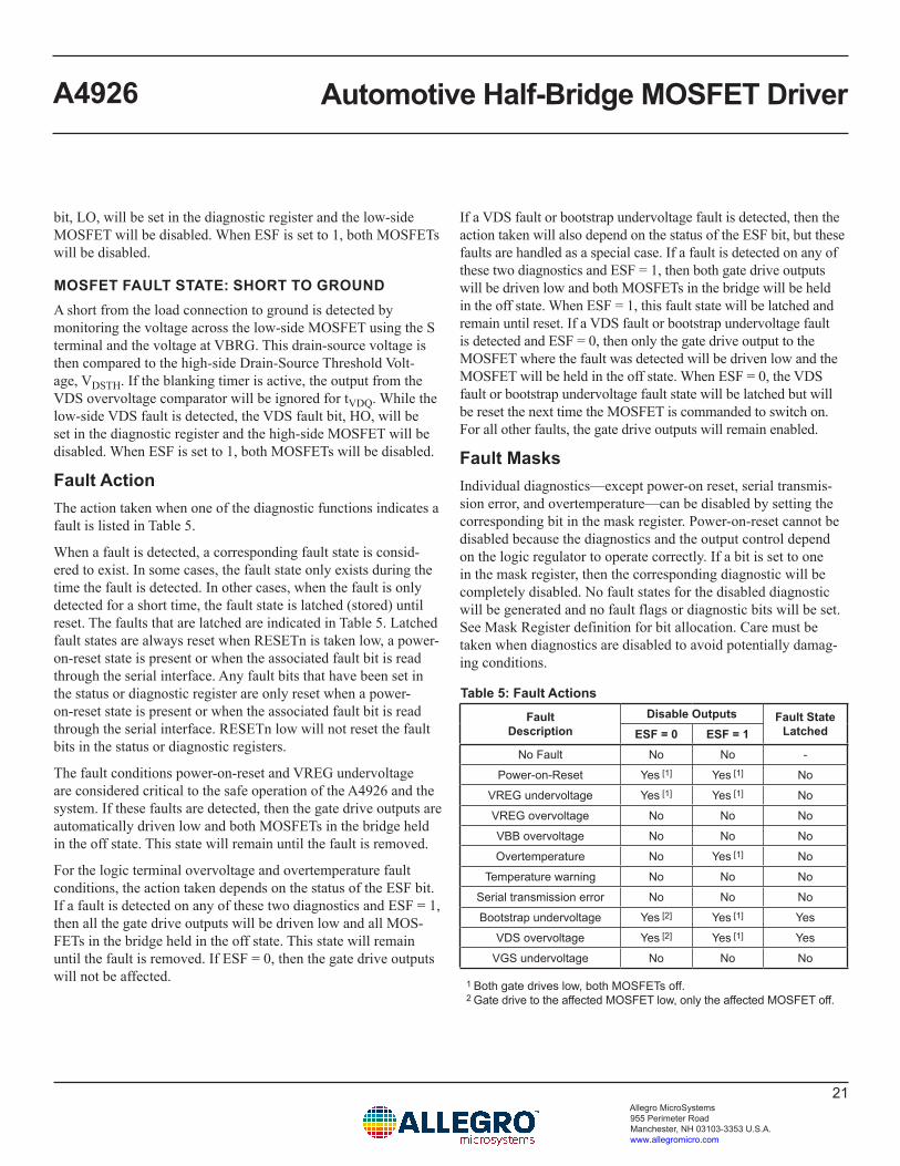
Fault ActionThe action taken when one of the diagnostic functions indicates a fault is listed in Table 5.
When a fault is detected, a corresponding fault state is consid-ered to exist. In some cases, the fault state only exists during the time the fault is detected. In other cases, when the fault is only detected for a short time, the fault state is latched (stored) until reset. The faults that are latched are indicated in Table 5. Latched fault states are always reset when RESETn is taken low, a power-on-reset state is present or when the associated fault bit is read through the serial interface. Any fault bits that have been set in the status or diagnostic register are only reset when a power-on-reset state is present or when the associated fault bit is read through the serial interface. RESETn low will not reset the fault bits in the status or diagnostic registers.
The fault conditions power-on-reset and VREG undervoltage are considered critical to the safe operation of the A4926 and the system. If these faults are detected, then the gate drive outputs are automatically driven low and both MOSFETs in the bridge held in the off state. This state will remain until the fault is removed.
For the logic terminal overvoltage and overtemperature fault conditions, the action taken depends on the status of the ESF bit. If a fault is detected on any of these two diagnostics and ESF = 1, then all the gate drive outputs will be driven low and all MOS-FETs in the bridge held in the off state. This state will remain until the fault is removed. If ESF = 0, then the gate drive outputs will not be affected.
If a VDS fault or bootstrap undervoltage fault is detected, then the action taken will also depend on the status of the ESF bit, but these faults are handled as a special case. If a fault is detected on any of these two diagnostics and ESF = 1, then both gate drive outputs will be driven low and both MOSFETs in the bridge will be held in the off state. When ESF = 1, this fault state will be latched and remain until reset. If a VDS fault or bootstrap undervoltage fault is detected and ESF = 0, then only the gate drive output to the MOSFET where the fault was detected will be driven low and the MOSFET will be held in the off state. When ESF = 0, the VDS fault or bootstrap undervoltage fault state will be latched but will be reset the next time the MOSFET is commanded to switch on. For all other faults, the gate drive outputs will remain enabled.
Fault MasksIndividual diagnostics—except power-on reset, serial transmis-sion error, and overtemperature—can be disabled by setting the corresponding bit in the mask register. Power-on-reset cannot be disabled because the diagnostics and the output control depend on the logic regulator to operate correctly. If a bit is set to one in the mask register, then the corresponding diagnostic will be completely disabled. No fault states for the disabled diagnostic will be generated and no fault flags or diagnostic bits will be set. See Mask Register definition for bit allocation. Care must be taken when diagnostics are disabled to avoid potentially damag-ing conditions.
Table 5: Fault ActionsFault
DescriptionDisable Outputs Fault State
LatchedESF = 0 ESF = 1No Fault No No -
Power-on-Reset Yes [1] Yes [1] No
VREG undervoltage Yes [1] Yes [1] No
VREG overvoltage No No No
VBB overvoltage No No No
Overtemperature No Yes [1] No
Temperature warning No No No
Serial transmission error No No No
Bootstrap undervoltage Yes [2] Yes [1] Yes
VDS overvoltage Yes [2] Yes [1] Yes
VGS undervoltage No No No
1 Both gate drives low, both MOSFETs off.2 Gate drive to the affected MOSFET low, only the affected MOSFET off.

Automotive Half-Bridge MOSFET DriverA4926
22Allegro MicroSystems 955 Perimeter Road Manchester, NH 03103-3353 U.S.A.www.allegromicro.com
Table 6: Serial Register Definition*15 14 13 12 11 10 9 8 7 6 5 4 3 2 1 0
0: Config 0 0 0 0 0 WRDT5 DT4 DT3 DT2 DT1 DT0
P0 0 0 0 1 0 0 0 0 0
1: Config 1 0 0 0 1 WRVT5 VT4 VT3 VT2 VT1 VT0
P0 0 0 0 0 1 1 0 0 0
2: Config 2 0 0 1 0 WRVDQ
P0 0 0 0 0 0 0 0 0 0
3: Config 3 0 0 1 1 WRTVD5 TVD4 TVD3 TVD2 TVD1 TVD0
P0 0 0 0 0 1 0 0 0 0
4: Config 4 0 1 0 0 WRVRG
P0 0 0 1 0 0 0 0 0 0
6: Config 6 0 1 1 0 WRTR3 TR2 TR1 TR0 TF3 TF2 TF1 TF0
P0 0 0 0 0 1 0 0 0 1
7: Config 7 0 1 1 1 WRIR13 IR12 IR11 IR10 IF13 IF12 IF11 IF10
P0 0 0 0 0 0 0 0 0 0
8: Config 8 1 0 0 0 WRIR23 IR22 IR21 IR20 IF23 IF22 IF21 IF20
P0 0 0 0 0 0 0 0 0 0
10: Mask 0 1 0 1 0 WRVBS TW HU LU
P0 0 0 0 0 0 0 0 0 0
11: Mask 1 1 0 1 1 WRVRO VRU VSO HO LO
P0 0 0 0 0 0 0 0 0 0
12: Diag 0 1 1 0 0 0HU LU
P0 0 0 0 0 0 0 0 0 0
13: Diag 1 1 1 0 1 0VRO VRU HO LO
P0 0 0 0 0 0 0 0 0 0
14: Diag 2 1 1 1 0 0VSO VBS
P0 0 0 0 0 0 0 0 0 0
*Power-on reset value shown below each input register bit.
Continued on the next page...
SERIAL INTERFACE

Automotive Half-Bridge MOSFET DriverA4926
23Allegro MicroSystems 955 Perimeter Road Manchester, NH 03103-3353 U.S.A.www.allegromicro.com
Table 6:Serial Register Definition (continued)15 14 13 12 11 10 9 8 7 6 5 4 3 2 1 0
15: Control 1 1 1 1 WRDBM ESF HSR LSR
P0 0 0 1 0 0 0 0 0 0
StatusFF POR SE OT TW VS VR VBS GSU DSO
P1 1 0 0 0 0 0 0 0 0 0 0 0 0 0
*Power-on reset value shown below each input register bit.
A three-wire synchronous serial interface, compatible with SPI, is used to control the features of the A4926. The SDO terminal can be used, during a serial transfer, to provide diagnostic feedback and readback of the register contents.
The A4926 can be operated without the serial interface using the default settings and the logic control inputs; however, application specific configurations are only possible by setting the appropri-ate register bits through the serial interface. In addition to setting the configuration bits, the serial interface can also be used to control the bridge MOSFETs directly.
The serial interface timing requirements are specified in the Electrical Characteristics table, and illustrated in Figure 3. Data is received on the SDI terminal and clocked through a shift register on the rising edge of the clock signal input on the SCK terminal. STRn is normally held high, and is only brought low to initiate a serial transfer. No data is clocked through the shift register when STRn is high, allowing multiple slave units to use common SDI and SCK connections. Each slave then requires an independent STRn connection. The SDO output assumes a high-impedance state when STRn is high, allowing a common data readback con-nection.
When 16 data bits have been clocked into the shift register, STRn must be taken high to latch the data into the selected register. When this occurs, the internal control circuits act on the new data and the registers are reset depending on the type of transfer.
If there are more than 16 rising edges on SCK or if STRn goes high and there are fewer than 16 rising edges on SCK—either being described as a framing error—the write will be cancelled without latching data to the register. The Status register will not be reset.
The first four bits, D[15:12], in a serial word, are the register address bits giving the possibility of 16 register addresses. The
fifth bit, WR (D[11]), is the write/read bit. When WR is 1, the following 10 bits, D[10:1], clocked in from the SDI terminal, are written to the addressed register. When WR is 0, then no data is written to the serial registers and the contents of the addressed register are clocked out on the SDO terminal.
The last bit in any serial transfer, D[0], is a parity bit (P) that is set to ensure odd parity in the complete 16-bit word. Odd parity means that the total number of 1s in any transfer should always be an odd number. This ensures that there is always at least one bit set to 1 and one bit set to 0 and allows detection of stuck-at faults on the serial input and output data connections. The parity bit is not stored but generated on each transfer.
In addition to the addressable registers, a read-only status register is output on SDO for all register addresses when WR is set to 1. For all serial transfers, the five bits output on SDO will always be the first five bits from the status register. Register data is output on the SDO terminal msb first while STRn is low and changes to the next bit on each falling edge of SCK. The first bit, which is always the FF bit from the status register, is output as soon as STRn goes low.
Registers 12, 13, and 14 contain diagnostic fault indicators and are read only. If the WR bit for these registers is set to 1, then the data input through SDI is ignored and the contents of the status register is clocked out on the SDO terminal then reset as for a normal write. No other action is taken. If the WR bit for these registers is set to 0, then the data input through SDI is ignored and the contents of the addressed register is clocked out on the SDO terminal and the addressed register is reset.
If a framing or parity error is detected, the SE bit is set in the Status register to indicate a data transfer error. This fault condi-tion can be cleared by a subsequent valid serial write or by a power-on-reset.

Automotive Half-Bridge MOSFET DriverA4926
24Allegro MicroSystems 955 Perimeter Road Manchester, NH 03103-3353 U.S.A.www.allegromicro.com
Configuration RegistersNine registers are used to configure the operating parameters of the A4926.
Config 0: Bridge timing settings:
• DT[5:0], a 6-bit integer to set the dead time, tDEAD, in 50 ns increments.
Config 1: Bridge monitor setting:
• VT[5:0], a 6-bit integer to set the drain-source threshold volt-age, VDST, in 50 mV increments.
Config 2: Bridge monitor setting:
• VDQ, selects the VDS qualifier mode, blank or debounce.
Config 3: Bridge monitor setting:
• TVD[5:0], a 6-bit integer to set the VDS fault verification time, tVDQ, in 100 ns increments.
Config 4: Regulator configuration:
• VRG, selects the regulator and gate drive voltage.
Config 6: Gate drive time setting:
• TR[3:0], a 4-bit integer to set the high-side and low-side I1 time in 50 ns increments.
• TF[3:0], a 4-bit integer to set the high-side and low-side I1 time in 50 ns increments.
Config 7: Gate drive current setting:
• IR1[3:0] , a 4-bit integer to set the MOSFET turn-on I1 Current in 4.5 mA increments.
• IF1[3:0] , a 4-bit integer to set the MOSFET turn-off I1 Current in 5.3 mA increments.
Config 8: Gate drive current setting:
• IR2[3:0] , a 4-bit integer to set the MOSFET turn-on I2 Current in 4.5 mA increments.
• IF2[3:0] , a 4-bit integer to set the MOSFET turn-off I2 Current in 5.3 mA increments.
Diagnostic RegistersIn addition to the read-only status register, five registers provide detailed diagnostic management and reporting. Two mask register allow individual diagnostics to be disabled and three read-only diagnostic registers provide fault bits for individual diagnostic tests and monitors. If a bit is set to one in the mask register, then the corresponding diagnostic will be completely disabled. No fault states for the disabled diagnostic will be generated and no fault flags or diagnostic bits will be set. These bits in the diagnos-tic registers are reset on completion of a successful read of the register.
Mask 0:
Individual bits to disable bootstrap (VBS), temperature warning (TW), and the VGS undervoltage diagnostic monitors (HU and LU).
Mask 1:
Individual bits to disable the voltage regulator (VRO, VRU and VSO) and the VDS overvoltage diagnostic monitors (HO and LO).
Diagnostic 0 (read only):
Individual bits indicating faults detected in VGS diagnostic moni-tors (HU and LU).
Diagnostic 1 (read only):
Individual bits indicating faults detected in voltage regulator (VRO and VRU) and VDS overvoltage diagnostic monitors (HO and LO).
Diagnostic 2 (read only):
Individual bits indicating faults detected in the VBB supply volt-age (VBS).
Control RegisterThe Control register contains one control bit for each MOSFET and some system function settings:
• DBM, disabled bootstrap management function.• ESF, defines the action taken when a short is detected. See
diagnostics section for details of fault actions.• HSR and LSR, MOSFET Control bits.

Automotive Half-Bridge MOSFET DriverA4926
25Allegro MicroSystems 955 Perimeter Road Manchester, NH 03103-3353 U.S.A.www.allegromicro.com
Status RegisterThere is one status register in addition to the 16 addressable registers. When any register transfer takes place, the first five bits output on SDO are always the most significant five bits of the status register regardless of whether the addressed register is being read or written. (see serial timing diagram).
The content of the remaining eleven bits will depend on the state of the WR bit input on SDI. When WR is 1, the addressed register will be written and the remaining eleven bits output on SDO will be the least significant ten bits of the status register followed by a parity bit. When WR is 0, the addressed register will be read and the remaining eleven bits will be the contents of the addressed register followed by a parity bit.
The read-only status register provides a summary of the chip sta-tus by indicating if any diagnostic monitors have detected a fault. The most significant three bits of the status register (FF, POR, and SE) indicate critical system faults. Bits OT and TW provide indicators for specific individual monitors and the remaining bits are derived from the contents of the three diagnostic registers. The contents and mapping to the diagnostic registers are listed in Table 7.
Table 7: Status Register MappingStatus
Register Bit Diagnostic
Related Diagnostic Register Bits
FF Status Flag None
POR Power-on-reset None
SE Serial Error None
OT Overtemperature None
TW Temperature warning None
VS VBB Monitor VSO
VR VREG monitor VRU, VRO
VBS Bootstrap UV VBS
GSU VGS UV HU, LU
DSO VDS OV HO, LO
UV = Undervoltage, OV = Overvoltage
The read-only status register provides a summary of the chip status by indicating if any diagnostic monitors have detected a fault. The most significant three bits of the status register (FF, POR, and SE) indicate critical system faults. Bits OT and TW
provide indicators for specific individual monitors and the remaining bits are derived from the contents of the three diagnos-tic registers. The contents and mapping to the diagnostic registers is listed in Table 7.
The first most significant bit in the register is the diagnostic status flag, FF. This is high if any bits in the status register are set. When STRn goes low to start a serial write, the SDO outputs the diagnostic status flag. This allows the main controller to poll the A4926 through the serial interface to determine if a fault has been detected. If no faults have been detected, then the serial transfer may be terminated without generating a serial read fault by ensur-ing that SCK remains high while STRn is low. When STRn goes high, the transfer will be terminated and SDO will go into its high-impedance state.
The second most significant bit is the POR bit. At power-up or after a power-on-reset, the FF bit and the POR bit are set, indi-cating to the external controller that a power-on-reset has taken place. All other diagnostic bits are reset and all other registers are returned to their default state. Note that a power-on-reset only occurs when the output of the internal logic regulator rises above its undervoltage threshold. Power-on-reset is not affected by the state of the VBB supply or the VREG regulator output. In general, the VR and VRU bits will also be set following a power-on-reset as the regulators will not have reached their respective rising undervoltage thresholds until after the register reset is completed.
The third bit in the status register is the SE bit, which indicates that the previous serial transfer was not completed successfully.
Bits OT and TW are the fault bits for the two temperature moni-tors. If one or more of these faults are no longer present, then the corresponding fault bits will be reset following a successful read of the status register. Resetting only affects latched fault bits for faults that are no longer present. For any static faults that are still present, for example overtemperature, the fault flag will remain set after the reset.
The remaining bits, VS, VR, VBS, GSU, and DSO are all derived from the contents of the diagnostic registers. These bits are only cleared when the corresponding contents of the diagnostic are read and reset, they cannot be reset by reading the status register. A fault indicated on any of the related diagnostic register bits will set the corresponding status bit to 1. The related diagnostic register must then be read to determine the exact fault and clear the fault state if the fault condition has cleared.

Automotive Half-Bridge MOSFET DriverA4926
26Allegro MicroSystems 955 Perimeter Road Manchester, NH 03103-3353 U.S.A.www.allegromicro.com
SERIAL REGISTER REFERENCE15 14 13 12 11 10 9 8 7 6 5 4 3 2 1 0
0: Config 0 0 0 0 0 WRDT5 DT4 DT3 DT2 DT1 DT0
P0 0 0 0 1 0 0 0 0 0
1: Config 1 0 0 0 1 WRVT5 VT4 VT3 VT2 VT1 VT0
P0 0 0 0 0 1 1 0 0 0
2: Config 2 0 0 1 0 WRVDQ
P0 0 0 0 0 0 0 0 0 0
3: Config 3 0 0 1 1 WRTVD5 TVD4 TVD3 TVD2 TVD1 TVD0
P0 0 0 0 0 1 0 0 0 0
4: Config 4 0 1 0 0 WRVRG
P0 0 0 1 0 0 0 0 0 0
Config 0
DT[5:0] Dead time.tDEAD = n × 50 nswhere n is a positive integer defined by DT[5:0],e.g. for the power-on-reset conditionDT[5:0] = [10 0000] then tDEAD = 1.6 µs.The range of tDEAD is 100 ns to 3.15 µs. Selecting a value of 1 or 2 will set the dead time to 100 ns. A value of zero disables the dead time.
Config 1
VT[5:0] VDS overvoltage threshold.VDST = n × 50 mVwhere n is a positive integer defined by VT[5:0],e.g. for the power-on-reset conditionVT[5:0] = [01 1000] then VDST = 1.2 V.The range of VDST is 0 to 3.15 V.
Config 2
VDQ VDS Fault qualifier mode.VDQ VDS Fault Qualifier Default
0 Debounce D1 Blank
Config 3
TVD[5:0] VDS verification time.tVDQ = n × 100 nswhere n is a positive integer defined by TVD[5:0],e.g. for the power-on-reset condition.TVD[5:0] = [01 0000] then tVDQ = 1.6 µs.The range of tVDQ is 0 to 6.3 µs.
Config 4
VRG VREG Voltage Level.VRG VREG Voltage Default
0 8 V1 11 V D

Automotive Half-Bridge MOSFET DriverA4926
27Allegro MicroSystems 955 Perimeter Road Manchester, NH 03103-3353 U.S.A.www.allegromicro.com
15 14 13 12 11 10 9 8 7 6 5 4 3 2 1 0
6: Config 6 0 1 1 0 WRTR3 TR2 TR1 TR0 TF3 TF2 TF1 TF0
P0 0 0 0 0 1 0 0 0 1
7: Config 7 0 1 1 1 WRIR13 IR12 IR11 IR10 IF13 IF12 IF11 IF10
P0 0 0 0 0 0 0 0 0 0
8: Config 8 1 0 0 0 WRIR23 IR22 IR21 IR20 IF23 IF22 IF21 IF20
P0 0 0 0 0 0 0 0 0 0
SERIAL REGISTER REFERENCE (continued)
Config 6
TR[3:0] MOSFET turn-on t1 time.t1 = (n + 1) × 50 nswhere n is a positive integer defined by TR[3:0],e.g. if TR[3:0] = [0001] then t1 = 100 ns.The range of t1 is 50 to 800 ns.
TF[3:0] MOSFET turn-off t1 time.t1 = (n + 1) × 50 nswhere n is a positive integer defined by TF[3:0],e.g. for the power-on-reset conditionTF[3:0] = [0001] then t1 = 100 ns.The range of t1 is 50 to 800 ns.
Config 7
IR1[3:0] MOSFET turn-on I1 Current.I1 = n × –4.5 mAwhere n is a positive integer defined by IR1[3:0],e.g. if IR1[3:0] = [1000] then I1 = –36 mAThe range of I1 is –4.5 mA to –67.5 mA. Selecting a value of 0 will set maximum gate drive to turn on the MOSFET as quickly as possible.
IF1[3:0] MOSFET turn-off I1 Current.I1 = n × 5.3 mAwhere n is a positive integer defined by IF1[3:0],e.g. if IF1[3:0] = [1000] then I1 = 42.4 mA.The range of I1 is 5.3 to 79.5 mA. Selecting a value of 0 will set maximum gate drive to turn on the MOSFET as quickly as possible.
Config 8
IR2[3:0] MOSFET turn-on I2 Current.I2 = n × –4.5 mAwhere n is a positive integer defined by IR2[3:0],e.g. if IR2[3:0] = [1000] then I2 = –36 mA.The range of I2 is –4.5 to –67.5 mA. Selecting a value of 0 will set maximum gate drive to turn on the MOSFET as quickly as possible.
IF2[3:0] MOSFET turn-off I2 Current.I2 = n × 5.3 mAwhere n is a positive integer defined by IF2[3:0],e.g. if IF2[3:0] = [1000] then I2 = 42.4 mA.The range of I2 is 5.3 to 79.5 mA. Selecting a value of 0 will set maximum gate drive to turn on the MOSFET as quickly as possible.

Automotive Half-Bridge MOSFET DriverA4926
28Allegro MicroSystems 955 Perimeter Road Manchester, NH 03103-3353 U.S.A.www.allegromicro.com
15 14 13 12 11 10 9 8 7 6 5 4 3 2 1 0
10: Mask 0 1 0 1 0 WRVBS TW HU LU
P0 0 0 0 0 0 0 0 0 0
11: Mask 1 1 0 1 1 WRVRO VRU VSO HO LO
P0 0 0 0 0 0 0 0 0 0
SERIAL REGISTER REFERENCE (continued)
Mask 0
VBS Bootstrap Undervoltage
TW Temperature Warning
HU High-Side VGS Undervoltage
LU Low-Side VGS Undervoltage
xxx Fault Mask Default0 Fault detection permitted D1 Fault detection disabled
Mask 1
VRO VREG Overvoltage
VRU VREG Undervoltage
VSO VBB Overvoltage
HO High-Side VDS Overvoltage
LO Low-Side VDS Overvoltage

Automotive Half-Bridge MOSFET DriverA4926
29Allegro MicroSystems 955 Perimeter Road Manchester, NH 03103-3353 U.S.A.www.allegromicro.com
SERIAL REGISTER REFERENCE (continued)15 14 13 12 11 10 9 8 7 6 5 4 3 2 1 0
12: Diag 0 1 1 0 0 0HU LU
P0 0 0 0 0 0 0 0 0 0
13: Diag 1 1 1 0 1 0VRO VRU HO LO
P0 0 0 0 0 0 0 0 0 0
14: Diag 2 1 1 1 0 0VSO VBS
P0 0 0 0 0 0 0 0 0 0
StatusFF POR SE OT TW VS VR VBS GSU DSO
P1 1 0 0 0 0 0 0 0 0 0 0 0 0 0
Diag 0 (read only)
HU High-Side VGS Undervoltage
LU Low-Side VGS Undervoltage
Diag 1 (read only)
VRO VREG Overvoltage
VRU VREG Undervoltage
HO High-Side VDS Overvoltage
LO Low-Side VDS Overvoltage
Diag 2 (read only)
VSO VBB Overvoltage
VBS Bootstrap Undervoltage
xxx Status0 No fault detected1 Fault detected
Status (read only)
FF Diagnostic Register Flag
POR Power-On-Reset
SE Serial Error
OT Overtemperature
TW High Temperature Warning
VS VBB Fault
VR VREG Out of Range
VBS Bootstrap Undervoltage
GSU VGS Undervoltage
DSO VDS Overvoltage
xxx Status0 No fault detected1 Fault detected
Status Register Bit Mapping
Status Register Bit
Related Diagnostic Register Bits
FF None
POR None
SE None
OT None
TW None
VS VSO
VR VRU, VRO
VBS VBS
GSU HU, LU
DSO HO, LO
U = Undervoltage, O = Overvoltage

Automotive Half-Bridge MOSFET DriverA4926
30Allegro MicroSystems 955 Perimeter Road Manchester, NH 03103-3353 U.S.A.www.allegromicro.com
15 14 13 12 11 10 9 8 7 6 5 4 3 2 1 0
15: Control 1 1 1 1 WRDBM ESF HSR LSR
P0 0 0 1 0 0 0 0 0 0
SERIAL REGISTER REFERENCE (continued)
Control
DBMDBM Bootstrap manager Default
0 Active D1 Disabled
ESF Enable Stop on Fail.ESF Recirculation Default
0 No stop on fail. Report fault.1 Stop on fail. Report fault. D
HSR High-side gate drive
LSR Low-side gate driveSee Table 2 and Table 3 for control logic operation.

Automotive Half-Bridge MOSFET DriverA4926
31Allegro MicroSystems 955 Perimeter Road Manchester, NH 03103-3353 U.S.A.www.allegromicro.com
Dead-Time SelectionThe choice of power MOSFET and external series gate resistance determines the selection of the dead time. The dead time, tDEAD, should be made long enough to ensure that one MOSFET has stopped conducting before the complementary MOSFET starts conducting. This should also account for the tolerance and varia-tion of the MOSFET gate capacitance, the series gate resistance and the on-resistance of the driver in the A4926.
tDEAD
Vt0
VGHA-VSA
VGLA
VGSL
VGSH
Figure 7: Minimum Dead TimeFigure 7 shows the typical switching characteristics of a pair of complementary MOSFETs. Ideally, one MOSFET should start to turn on just after the other has completely turned off. The point at which a MOSFET starts to conduct is the threshold voltage Vt0. The dead time should be long enough to ensure that the gate-source voltage of the MOSFET that is switching off is just below Vt0 before the gate-source voltage of the MOSFET that is switch-ing on rises to Vt0. This will be the minimum theoretical dead time, but in practice the dead time will have to be longer than this to accommodate variations in MOSFET and driver parameters for process variations and overtemperature.
Bootstrap Capacitor SelectionThe A4926 requires a bootstrap capacitor C. To simplify this description of the bootstrap capacitor selection criteria, generic naming is used here. So, for example, CBOOT, QBOOT, and VBOOT refer to the bootstrap capacitor, and QGATE refers to any of the two associated MOSFETs. CBOOT must be correctly selected to ensure proper operation of the device—too large and time will be wasted charging the capacitor, resulting in a limit on the maxi-mum duty cycle and PWM frequency; too small and there can be a large voltage drop at the time the charge is transferred from CBOOT to the MOSFET gate.
To keep the voltage drop due to charge sharing small, the charge
in the bootstrap capacitor, QBOOT, should be much larger than QGATE, the charge required by the gate:
QBOOT >> QGATE
A factor of 20 is a reasonable value, so
QBOOT = CBOOT × VBOOT = QGATE × 20
or
=QGATE × 20CBOOT
VBOOT
where VBOOT is the voltage across the bootstrap capacitor.
The voltage drop, ∆V, across the bootstrap capacitor as the MOS-FET is being turned on, can be approximated by:
=CBOOT
QGATE∆V
so for a factor of 20, ∆V will be 5% of VBOOT.
The maximum voltage across the bootstrap capacitor under normal operating conditions is VREG (max). However in some circumstances the voltage may transiently reach a maximum of 18 V, which is the clamp voltage of the Zener diode between the C terminal and the S terminal. In most applications with a good ceramic capacitor, the working voltage can be limited to 16 V.
Bootstrap ChargingIt is good practice to ensure the high-side bootstrap capacitor is completely charged before a high-side PWM cycle is requested. The time required to charge the capacitor, tCHARGE , in µs, is approximated by:
=100
CBOOT × ∆VtCHARGE
where CBOOT is the value of the bootstrap capacitor in nF and ∆V is the required voltage of the bootstrap capacitor. At power up and when the drivers have been disabled for a long time, the bootstrap capacitor can be completely discharged. In this case, ∆V can be considered to be the full high-side drive voltage, 12 V. Otherwise, ∆V is the amount of voltage dropped during the charge transfer, which should be 400 mV or less. The capacitor is charged when-ever the S terminal is pulled low and current flows from the capaci-tor connected to the VREG terminal through the internal bootstrap diode circuit to CBOOT.
APPLICATION INFORMATION

Automotive Half-Bridge MOSFET DriverA4926
32Allegro MicroSystems 955 Perimeter Road Manchester, NH 03103-3353 U.S.A.www.allegromicro.com
VREG Capacitor SelectionThe internal reference, VREG, supplies current for the low-side gate-drive circuits and the charging current for the bootstrap capacitors. When a low-side MOSFET is turned on, the gate-drive circuit will provide the high transient current to the gate that is necessary to turn the MOSFET on quickly. This current, which can be several hundred milliamperes, cannot be provided directly by the limited output of the VREG regulator but must be supplied by an external capacitor, CREG, connected between the VREG terminal and GND
The turn-on current for the high-side MOSFET is similar in value but is mainly supplied by the bootstrap capacitor. However, the bootstrap capacitor must then be recharged from CREG through the VREG terminal. Unfortunately, the bootstrap recharge can occur a very short time after the low-side turn on occurs. This
means that the value of CREG between VREG and GND should be high enough to minimize the transient voltage drop on VREG for the combination of a low-side MOSFET turn on and a bootstrap capacitor recharge. For block commutation control (trapezoidal drive), where only one high side and one low side are switching during each PWM period, a minimum value of 20 × CBOOT is reasonable. For sinusoidal control schemes, a minimum value of 40 × CBOOT is recommended. As the maximum work-ing voltage of CREG will never exceed VREG, the part’s voltage rating can be as low as 15 V. However, it is recommended that a capacitor rated to at least twice the maximum working volt-age should be used to reduce any impact operating voltage may have on capacitance value. For best performance, CREG should be ceramic rather than electrolytic. CREG should be mounted as close to the VREG terminal as possible.

Automotive Half-Bridge MOSFET DriverA4926
33Allegro MicroSystems 955 Perimeter Road Manchester, NH 03103-3353 U.S.A.www.allegromicro.com
INPUT/OUTPUT STRUCTURES
C
16 V
GH
S
GL
LSS
16 V
16 V
VREG
56 V
SDISCK
2 kΩ
7.5 V 6 V50 kΩ
VDL
VBRG
56 V
VBB
56 V
DL
6 V
CP1
20 V
CP2 VREG
16 V
6 V
BIAS
RESETnENABLE
HS
2 kΩ
56 V
50 kΩ
DIAG25 Ω
56 V
STRn2 kΩ
7.5 V 6 V
50 kΩ
VDL VDL
SDO50 Ω
7.5 V
VDL
BIAS
LSn 2 kΩ
56 V
170 kΩ
VDL
7.5 V
Figure 8a: Gate Drive Outputs Figure 8b: Supplies
Figure 8c: SDI, SCK Inputs Figure 8d: STRn Inputs Figure 8e: RESETn, ENABLE, HS Inputs
Figure 8f: SDO Output Figure 8g: DIAG Output Figure 8h: LSn Input

Automotive Half-Bridge MOSFET DriverA4926
34Allegro MicroSystems 955 Perimeter Road Manchester, NH 03103-3353 U.S.A.www.allegromicro.com
LAYOUT RECOMMENDATIONSCareful consideration must be given to PCB layout when design-ing high-frequency, fast-switching, high-current circuits:• The exposed thermal pad should be connected to the GND
terminal.• Minimize stray inductance by using short, wide copper tracks
at the drain and source terminals of all power MOSFETs. This includes load lead connections, the input power bus.This will minimize voltages induced by fast switching of large load currents.
• Consider the addition of small (100 nF) ceramic decoupling capacitor across the source and drain of the power MOSFETs to limit fast transient voltage spikes caused by track inductance.
• Keep the gate discharge return connections S and LSS as short as possible. Any inductance on these tracks will cause negative transitions on the corresponding A4926 terminals, which may exceed the absolute maximum ratings. If this is likely, consider the use of clamping diodes to limit the negative excursion on these terminals with respect to the GND terminal.
• Supply decoupling, typically a 100 nF ceramic capacitor, should be connected between VBB and GND as close to the A4926 terminals as possible.
• Supply decoupling should be connected between VREG and
GND as close to the A4926 terminals as possible.• Check the peak voltage excursion of the transients on the
LSS terminals with reference to the GND terminal using a close-grounded (“tip & barrel”) probe. If the voltage at any LSS terminal exceeds the absolute maximum in the datasheet, add additional clamping and/or capacitance between the LSS terminal and the GND terminal.
• Gate charge drive paths and gate discharge return paths may carry a large transient current pulse. Therefore, the traces from GH, GL, S, and LSS should be as short as possible to reduce the trace inductance.
• Provide an independent connection between the LSS terminal to the source of the low-side MOSFET in the power bridge. Connection of the LSS terminal directly to the GND terminal is not recommended as this may inject noise into sensitive functions such as the various voltage monitors.
• A low-cost diode can be placed in the connection to VBB to provide reverse battery protection. In reverse battery conditions, it is possible to use the body diodes of the power MOSFETs to clamp the reverse voltage to approximately 4 V. In this case, the additional diode in the VBB connection will prevent damage to the A4926 and the VBRG input will survive the reverse voltage.
Figure 9: Supply Routing Suggestions
Supply Common
+ Supply
Load
PAD
S
GH
GL
LSS
VBB
VREG
Controller Supply GroundPower Ground
A4926
VBRG
GND
Optional reverse battery protection

Automotive Half-Bridge MOSFET DriverA4926
35Allegro MicroSystems 955 Perimeter Road Manchester, NH 03103-3353 U.S.A.www.allegromicro.com
PACKAGE OUTLINE DRAWING
Figure 10: Package LP, 20-Lead TSSOP with Exposed Pad
For Reference Only – Not for Tooling Use(Reference JEDEC MO-153ACT; Allegro DWG-0000379, Rev. 3)
NOT TO SCALEDimensions in millimeters
Dimensions exclusive of mold flash, gate burrs, and dambar protrusionsExact case and lead configuration at supplier discretion within limits shown
A
1.20 MAX
0.150.025
0.300.19
0.200.09
8°0°
0.60 ±0.15
1.00 REF
C
SEATINGPLANE
C0.10
20X
0.65 BSC
0.25 BSC
21
1
20
6.50 ±0.10
4.40 ±0.103.00 3.00
4.20
4.20
6.40 ±0.20
GAUGE PLANE
SEATING PLANE
A
B
0.45
1.70
20
21
B
6.10
0.65
C Exposed thermal pad (bottom surface)
C
PCB Layout Reference View
Terminal #1 mark area
Reference land pattern layout (reference IPC7351 SOP65P640X110-21M); all pads a minimum of 0.20 mm from all adjacent pads;adjust as necessary to meet application process requirements and PCB layout tolerances; when mounting on a multilayer PCB,thermal vias at the exposed thermal pad land can improve thermal dissipation (reference EIA/JEDEC Standard JESD51-5)
Branding scale and appearance at supplier discretionD
XXXXXXXDate Code
Lot Number
D Standard Branding Reference View Line 1, 2, 3 = 8 characters
Line 1: Part NumberLine 2: Logo A, 4 digit Date CodeLine 3: Characters 5, 6, 7, 8 of Assembly Lot Number

Automotive Half-Bridge MOSFET DriverA4926
36Allegro MicroSystems 955 Perimeter Road Manchester, NH 03103-3353 U.S.A.www.allegromicro.com
For the latest version of this document, visit our website:www.allegromicro.com
Revision HistoryNumber Date Description
– March 21, 2017 Initial release
1 April 11, 2017 Corrected Serial Register Reference, Config 7 and 8 (page 27).
2 April 24, 2017 Added DIAG Output section and updated Status and Diagnostic Registers section (page 17).
3 February 11, 2019 Minor editorial updates
4 February 28, 2020 Minor editorial updates
5 February 23, 2022 Updated package drawing (page 35)
Copyright 2022, Allegro MicroSystems.Allegro MicroSystems reserves the right to make, from time to time, such departures from the detail specifications as may be required to permit
improvements in the performance, reliability, or manufacturability of its products. Before placing an order, the user is cautioned to verify that the information being relied upon is current.
Allegro’s products are not to be used in any devices or systems, including but not limited to life support devices or systems, in which a failure of Allegro’s product can reasonably be expected to cause bodily harm.
The information included herein is believed to be accurate and reliable. However, Allegro MicroSystems assumes no responsibility for its use; nor for any infringement of patents or other rights of third parties which may result from its use.
Copies of this document are considered uncontrolled documents.


