Embed Size (px)
Citation preview

A40i Datasheet Intelligent Industrial Control Processor
Revision 1.0
May. 22, 2018
Copyright © 2018 Allwinner Technology Co.,Ltd. All Rights Reserved.

Revision History
A40i Datasheet(Revision 1.0) Copyright© 2018 Allwinner Technology Co.,Ltd. All Rights Reserved. Page 2
Revision History
Revision Date Description
1.0 May.22,2018 Initial release version.

Declaration
A40i Datasheet(Revision 1.0) Copyright© 2018 Allwinner Technology Co.,Ltd. All Rights Reserved. Page 3
Declaration
THIS DOCUMENTATION IS THE ORIGINAL WORK AND COPYRIGHTED PROPERTY OF ALLWINNER TECHNOLOGY (“ALLWINNER”). REPRODUCTION IN WHOLE OR IN PART MUST OBTAIN THE WRITTEN APPROVAL OF ALLWINNER AND GIVE CLEAR ACKNOWLEDGEMENT TO THE COPYRIGHT OWNER.
THE PURCHASED PRODUCTS, SERVICES AND FEATURES ARE STIPULATED BY THE CONTRACT MADE BETWEEN ALLWINNER AND THE CUSTOMER. PLEASE READ THE TERMS AND CONDITIONS OF THE CONTRACT AND RELEVANT INSTRUCTIONS CAREFULLY BEFORE USING, AND FOLLOW THE INSTRUCTIONS IN THIS DOCUMENTATION STRICTLY. ALLWINNER ASSUMES NO RESPONSIBILITY FOR THE CONSEQUENCES OF IMPROPER USE(INCLUDING BUT NOT LIMITED TO OVERVOLTAGE, OVERCLOCK, OR EXCESSIVE TEMPERATURE).
THE INFORMATION FURNISHED BY ALLWINNER IS PROVIDED JUST AS A REFERENCE OR TYPICAL APPLICATIONS, ALL STATEMENTS, INFORMATION, AND RECOMMENDATIONS IN THIS DOCUMENT DO NOT CONSTITUTE A WARRANTY OF ANY KIND, EXPRESS OR IMPLIED. ALLWINNER RESERVES THE RIGHT TO MAKE CHANGES IN CIRCUIT DESIGN AND/OR SPECIFICATIONS AT ANY TIME WITHOUT NOTICE.
NOR FOR ANY INFRINGEMENTS OF PATENTS OR OTHER RIGHTS OF THE THIRD PARTIES WHICH MAY RESULT FROM ITS USE. NO LICENSE IS GRANTED BY IMPLICATION OR OTHERWISE UNDER ANY PATENT OR PATENT RIGHTS OF ALLWINNER. THIRD PARTY LICENCES MAY BE REQUIRED TO IMPLEMENT THE SOLUTION/PRODUCT. CUSTOMERS SHALL BE SOLELY RESPONSIBLE TO OBTAIN ALL APPROPRIATELY REQUIRED THIRD PARTY LICENCES. ALLWINNER SHALL NOT BE LIABLE FOR ANY LICENCE FEE OR ROYALTY DUE IN RESPECT OF ANY REQUIRED THIRD PARTY LICENCE. ALLWINNER SHALL HAVE NO WARRANTY, INDEMNITY OR OTHER OBLIGATIONS WITH RESPECT TO MATTERS COVERED UNDER ANY REQUIRED THIRD PARTY LICENCE.

Contents
A40i Datasheet(Revision 1.0) Copyright© 2018 Allwinner Technology Co.,Ltd. All Rights Reserved. Page 4
Contents 1. Overview ....................................................................................................................................................................... 12
2. Features ......................................................................................................................................................................... 13
2.1. CPU Architecture ................................................................................................................................................ 13
2.2. GPU Architecture ............................................................................................................................................... 13
2.3. Memory Subsystem............................................................................................................................................ 13
2.4. System Peripheral ............................................................................................................................................... 14
2.5. Video Engine ...................................................................................................................................................... 15
2.6. Display Subsystem .............................................................................................................................................. 16
2.7. Image In ...............................................................................................................................................................17
2.8. Audio Subsystem .................................................................................................................................................17
2.9. External Peripherals ........................................................................................................................................... 18
2.10. Package .............................................................................................................................................................20
3. Block Diagram ............................................................................................................................................................... 21
4. Pin Description .............................................................................................................................................................. 23
4.1. Pin Characteristics .............................................................................................................................................. 23
4.2. Signal Descriptions ............................................................................................................................................. 50
5. Electrical Characteristics ................................................................................................................................................ 57
5.1. Absolute Maximum Ratings ................................................................................................................................ 57
5.2. Recommended Operating Conditions ................................................................................................................ 58
5.3. DC Electrical Characteristics ............................................................................................................................... 58
5.4. PLL Electrical Characteristics .............................................................................................................................. 59
5.4.1. CPU PLL Electrical Parameters ................................................................................................................. 59
5.4.2. Audio PLL Electrical Parameters .............................................................................................................. 59
5.4.3. GPU PLL Electrical Parameters ................................................................................................................ 59
5.4.4. Peripheral0/1 PLL Electrical Parameters .................................................................................................. 60

Contents
A40i Datasheet(Revision 1.0) Copyright© 2018 Allwinner Technology Co.,Ltd. All Rights Reserved. Page 5
5.4.5. MIPI PLL Electrical Parameters ................................................................................................................ 60
5.4.6. DDR0/1 PLL Electrical Parameters ........................................................................................................... 60
5.4.7. Video0/1 PLL Electrical Parameters ......................................................................................................... 60
5.4.8. VE PLL Electrical Parameters ................................................................................................................... 61
5.4.9. DE PLL Electrical Parameters ................................................................................................................... 61
5.4.10. SATA PLL Electrical Parameters .............................................................................................................. 61
5.5. KEYADC Electrical Characteristics ....................................................................................................................... 59
5.6. Oscillator Electrical Characteristics .................................................................................................................... 61
5.7. Maximum Current Consumption ........................................................................................................................62
5.8. External Memory Electrical Characteristics ........................................................................................................62
5.8.1. Nand AC Electrical Characteristics ............................................................................................................62
5.8.2. SMHC AC Electrical Characteristics ......................................................................................................... 66
5.9. External Peripherals Electrical Characteristics ....................................................................................................67
5.9.1. LCD AC Electrical Characteristics ..............................................................................................................67
5.9.2. CSI AC Electrical Characteristics .............................................................................................................. 69
5.9.3. EMAC AC Electrical Characteristics........................................................................................................... 70
5.9.4. PS2 AC Electrical Characteristics ............................................................................................................. 71
5.9.5. CIR AC Electrical Characteristics ............................................................................................................... 72
5.9.6. SPI AC Electrical Characteristics ............................................................................................................... 72
5.9.7. UART AC Electrical Characteristics ...........................................................................................................73
5.9.8. TWI AC Electrical Characteristics .............................................................................................................. 74
5.9.9. TSC AC Electrical Characteristics ............................................................................................................. 75
5.9.10. AC97 AC Electrical Characteristics ......................................................................................................... 75
5.9.11. SCR AC Electrical Characteristics ............................................................................................................78
5.10. Power-up and Power-down Sequence ............................................................................................................. 79
6. Package Thermal Characteristics ................................................................................................................................... 80
7. Pin Assignment .............................................................................................................................................................. 81
7.1. Pin Map .............................................................................................................................................................. 81

Contents
A40i Datasheet(Revision 1.0) Copyright© 2018 Allwinner Technology Co.,Ltd. All Rights Reserved. Page 6
7.2. Package Dimension .............................................................................................................................................82

Figures
A40i Datasheet(Revision 1.0) Copyright© 2018 Allwinner Technology Co.,Ltd. All Rights Reserved. Page 7
Figures
Figure 3-1. A40i Block Diagram ........................................................................................................................................... 21
Figure 3-2. A40i Application Diagram ................................................................................................................................. 22
Figure 5-1. Conventional Serial Access Cycle Timing (SAM0) ............................................................................................. 62
Figure 5-2. EDO Type Serial Access after Read Cycle Timing (SAM1) ................................................................................. 63
Figure 5-3. Extending EDO Type Serial Access Mode Timing (SAM2) ................................................................................. 63
Figure 5-4. Command Latch Cycle Timing ........................................................................................................................... 63
Figure 5-5. Address Latch Cycle Timing............................................................................................................................... 64
Figure 5-6. Write Data to Flash Cycle Timing ...................................................................................................................... 64
Figure 5-7. Waiting R/B# Ready Timing .............................................................................................................................. 64
Figure 5-8. WE# High to RE# Low Timing ............................................................................................................................ 65
Figure 5-9. RE# High to WE# Low Timing ............................................................................................................................ 65
Figure 5-10. Address to Data Loading Timing ..................................................................................................................... 65
Figure 5-11. SMHC in SDR Mode Output Timing ................................................................................................................ 66
Figure 5-12. SMHC in SDR Mode Input Timing ................................................................................................................... 66
Figure 5-13. HV_IF Interface Vertical Timing ...................................................................................................................... 67
Figure 5-14. HV_IF Interface Parallel Mode Horizontal Timing .......................................................................................... 68
Figure 5-15. HV_IF Interface Serial Mode Horizontal Timing ............................................................................................. 68
Figure 5-16. 8/10/12-bit CMOS Sensor Interface Timing.................................................................................................... 69
Figure 5-17. 16-bit YCbCr4:2:2 with Separate Sync Timing ................................................................................................ 69
Figure 5-18. 8-bit YCbCr4:2:2 with Embedded Syncs(BT656) Timing ................................................................................. 69
Figure 5-19. Data Sample Timing ........................................................................................................................................ 70
Figure 5-20. EMAC MII Interface Transmit Timing .............................................................................................................. 70
Figure 5-21. EMAC MII Interface Receive Timing................................................................................................................ 70
Figure 5-22. PS2 Timing for Master Transmit Data and Device Receive Data .................................................................... 71
Figure 5-23. PS2 Timing for Device Transmit Data and Master Receive Data .................................................................... 71

Figures
A40i Datasheet(Revision 1.0) Copyright© 2018 Allwinner Technology Co.,Ltd. All Rights Reserved. Page 8
Figure 5-24. PS2 Timing for Master Sending Command then Device Sending Response ................................................... 71
Figure 5-25. CIR-RX Timing .................................................................................................................................................. 72
Figure 5-26. SPI MOSI Timing .............................................................................................................................................. 72
Figure 5-27. SPI MISO Timing .............................................................................................................................................. 73
Figure 5-28. UART RX Timing .............................................................................................................................................. 73
Figure 5-29. UART nCTS Timing ........................................................................................................................................... 73
Figure 5-30. UART nRTS Timing ........................................................................................................................................... 74
Figure 5-31. TWI Timing ...................................................................................................................................................... 74
Figure 5-32. TSC Data and Clock Timing .............................................................................................................................. 75
Figure 5-33. AC97 Cold Reset Timing .................................................................................................................................. 75
Figure 5-34. AC97 Warm Reset Timing ............................................................................................................................... 75
Figure 5-35. AC-link Low Power Mode Timing .................................................................................................................... 76
Figure 5-36. BIT_CLK and SYNC Timing ............................................................................................................................... 76
Figure 5-37. AC-link Data Transmission Output and Input Timing...................................................................................... 76
Figure 5-38. Signal Rise and Fall Timing .............................................................................................................................. 76
Figure 5-39. SCR Activation and Cold Reset Timing ............................................................................................................ 78
Figure 5-40. SCR Warm Reset Timing.................................................................................................................................. 78
Figure 5-41. A40i Power Up Sequence ................................................................................................................................ 79
Figure 7-1. A40i Pin Map ..................................................................................................................................................... 81
Figure 7-2. A40i Package Dimension ................................................................................................................................... 82

Tables
A40i Datasheet(Revision 1.0) Copyright© 2018 Allwinner Technology Co.,Ltd. All Rights Reserved. Page 9
Tables Table 4-1. Pin Characteristics .............................................................................................................................................. 24
Table 4-2. Signal Descriptions ............................................................................................................................................. 50
Table 5-1. Absolute Maximum Ratings ............................................................................................................................... 57
Table 5-2. Recommended Operating Conditions ................................................................................................................ 58
Table 5-3. DC Electrical Characteristics ............................................................................................................................... 58
Table 5-4. KEYADC Electrical Characteristics....................................................................................................................... 59
Table 5-5. CPU PLL Electrical Parameters ........................................................................................................................... 59
Table 5-6. Audio PLL Electrical Parameters ......................................................................................................................... 59
Table 5-7. GPU PLL Electrical Parameters ........................................................................................................................... 59
Table 5-8. Peripheral0/1 PLL Electrical Parameters ............................................................................................................ 60
Table 5-9. MIPI PLL Electrical Parameters ........................................................................................................................... 60
Table 5-10. DDR0/1 PLL Electrical Parameters ................................................................................................................... 60
Table 5-11. Video0/1 PLL Electrical Parameters ................................................................................................................. 60
Table 5-12. VE PLL Electrical Parameters ............................................................................................................................ 61
Table 5-13. DE PLL Electrical Parameters ............................................................................................................................ 61
Table 5-14. SATA PLL Electrical Parameters ........................................................................................................................ 61
Table 5-15. 24MHz Crystal Characteristics ......................................................................................................................... 61
Table 5-16. 32768Hz Crystal Characteristics ....................................................................................................................... 62
Table 5-17. NAND Timing Constants ................................................................................................................................... 65
Table 5-18. SMHC Timing Constants ................................................................................................................................... 66
Table 5-19. LCD HV_IF Interface Timing Constants............................................................................................................. 68
Table 5-20. CSI Interface Timing Constants ........................................................................................................................ 70
Table 5-21. 100Mb/s MII Transmit Timing Constants ......................................................................................................... 70
Table 5-22. 100Mb/s MII Receive Timing Constants .......................................................................................................... 71
Table 5-23. PS2 Timing Constants ....................................................................................................................................... 71

Tables
A40i Datasheet(Revision 1.0) Copyright© 2018 Allwinner Technology Co.,Ltd. All Rights Reserved. Page 10
Table 5-24. CIR-RX Timing Constants .................................................................................................................................. 72
Table 5-25. SPI Timing Constants ........................................................................................................................................ 73
Table 5-26. UART Timing Constants .................................................................................................................................... 74
Table 5-27. TWI Timing Constants ...................................................................................................................................... 74
Table 5-28. TSC Timing Constants ....................................................................................................................................... 75
Table 5-29. AC97 Timing Constants .................................................................................................................................... 76
Table 5-30. SCR Timing Constants ....................................................................................................................................... 78
Table 6-1. A40i Thermal Resistance Characteristics ........................................................................................................... 80

About This Documentation
A40i Datasheet(Revision 1.0) Copyright© 2018 Allwinner Technology Co.,Ltd. All Rights Reserved. Page 11
About This Documentation
Purpose
The documentation describes features of each module, pin/signal characteristics, current consumption, PLL electrical characteristics, the interface timing, thermal and package of A40i processor. The documentation is intended to provide guidance to the hardware designers for electronics or sales personnel for electronic components. This documentation assumes that the reader has a background in electronic components. For details about register descriptions of each module, see the A40i User Manual.
Intended Audience The document is intended for: Hardware designers and maintenance personnel for electronics Sales personnel for electronic parts and components
Conventions Symbol Conventions The symbols that may be found in this document are defined as follows.
Symbol Description
WARNING
A warning means that injury or death is possible if the instructions are not obeyed.
CAUTION
A caution means that damage to equipment is possible.
NOTE
Provides additional information to emphasize or supplement important points of the main text.
Table Content Conventions The table content conventions that may be found in this document are defined as follows.
Symbol Description
- The cell is blank.
Numerical Conventions The expressions of data capacity, frequency, and data rate are described as follows.
Type Symbol Value
Data capacity
1K 1024
1M 1,048,576
1G 1,073,741,824
Frequency, data rate
1k 1000
1M 1,000,000
1G 1,000,000,000

Overview
A40i Datasheet(Revision 1.0) Copyright© 2018 Allwinner Technology Co.,Ltd. All Rights Reserved. Page 12
1. Overview
The A40i processor represents Allwinner’s latest achievement in intelligent industrial control processors. The processor is ideal for applications that require 3D graphics, advanced video processing, rich user interfaces, lower power consumption and higher system integration.
The A40i processor has some very exciting features:
CPU: A40i is based on quad-core CortexTM-A7 CPU architecture, the most power efficient CPU core ARM’s ever developed. GPU: A40i adopts the extensively implemented and technically mature Mali400 MP2 to provide mobile users with superior experience in web browsing, video playback and games. Video Engine: Supports mainstream high-definition video decoding including H.264, H.263, MPEG1/2/4, xvid, Sorenson Spark, VP6, VP8, AVS/AVS+, WMV7, WMV8 by 1080p@45fps. In the aspect of video encoding, the A40i supports 1080p@45fps H.264 encoding ability. Camera: Supports dual CMOS sensor parallel interfaces and 4-channel TVIN , which can easily finish multi-channel video recording. Display: Content can be displayed on 4-lane MIPI DSI displays, or RGB panel, or LVDS panel.TV-out on HDMI V1.4 is also supported. Audio: Integrated audio codec with 24bit/192kHz DAC playback, and supports I2S/PCM interface for connecting to an external audio codec.I2S/PCM interface includes eight channels of TDM with sampling precision up to 32bit/192kHz. Memory: Supports external memory interfaces to NAND Flash, SD/eMMC, Nor Flash and SDRAM port. SDRAM port can be configured to support LPDDR2, LPDDR3, DDR2, DDR3, DDR3L. Peripherals: To reduce total system cost, A40i has a broad range of hardware peripherals to meet the flexible peripheral configuration requirements such as UART, RTP, SPI, CIR, USB2.0 OTG, TWI etc.

Features
A40i Datasheet(Revision 1.0) Copyright© 2018 Allwinner Technology Co.,Ltd. All Rights Reserved. Page 13
2. Features
2.1. CPU Architecture • Quad-core ARM CortexTM-A7 Processor • ARMv7 ISA standard ARM instruction set • Thumb-2 Technology • Jazeller RCT • NEON Advanced SIMD • VFPv4 floating point • Large Physical Address Extensions(LPAE) • 32KB L1 Instruction cache and 32KB L1 Data cache for per CPU • 512KB L2 cache shared
2.2. GPU Architecture • Mali400 MP2 • Supports OpenGL ES 2.0 ,OpenGL ES 1.1, Open VG 1.1 standard
2.3. Memory Subsystem
Boot ROM
• On-chip 36KB ROM boot loader • Supports fast boot from NAND Flash, eMMC, SD/TF card and SPI Nor Flash • Supports system code download through USB OTG • Boot select pin(FEL) is used to select system boot method: boot from USB when FEL is low level, or else enter into
fast boot process
SDRAM
• Compatible with JEDEC standard DDR2/DDR3/DDR3L/LPDDR2/LPDDR3 SDRAM • Up to 2GB address space • 32-bit data bus width • Supports clock frequency up to 576MHz(DDR3/DDR3L)
NAND Flash
• Compliant with ONFI 2.3 and Toggle 1.0 • Up to 64-bit ECC per 512 bytes or 1024 bytes • Supports 1K/2K/4K/8K/16KB page size • Up to 8-bit data bus width • Supports 8 chip selects, and 2 ready_busy signals • Supports SLC/MLC NAND and EF-NAND

Features
A40i Datasheet(Revision 1.0) Copyright© 2018 Allwinner Technology Co.,Ltd. All Rights Reserved. Page 14
• Supports SDR/Toggle DDR/ONFI DDR NAND interface
SMHC
• Up to four SMHC controllers • Compatible with eMMC standard specification V5.0, SD physical layer specification V3.0 ,SDIO card specification
V2.0 • 1/4/8-bit bus width • Embedded special DMA to do data transfer • Supports hardware CRC generation and error detection • Supports block size of 1 to 65535 bytes
2.4. System Peripheral
Timer
• 6 Timers • Two 33-bit AVS counters to synchronize video and audio in the player • One watchdog to generate reset signal or interrupt • External 24MHz or 32768Hz crystal oscillator input
High Speed Timer
• 4 High Speed Timers • Clock source is fixed to AHBCLK, and the pre-scale ranges from 1 to 16 • 56-bit counter that can be separated to 24-bit high register and 32-bit low register
RTC
• Timer, Calendar, Alarm • Supports full clock features: second/minute/hour/day/month/year(with leap year)
GIC
• Supports 16 SGIs(Software Generated Interrupt), 16 PPIs(Private Peripheral Interrupt) and 101 SPIs(Shared Peripheral Interrupts)
• Supports ARM architecture security extensions • Supports ARM architecture virtualization extensions
DMA
• 16 channels • Interrupt generated for each DMA channel • Transfers data width of 8/16/32/64-bit • Supports linear and IO address modes • Programs the DMA burst size • Flexible data source and destination address generation • Supports data transfer types with memory-to-memory, memory-to-peripheral, peripheral-to-memory

Features
A40i Datasheet(Revision 1.0) Copyright© 2018 Allwinner Technology Co.,Ltd. All Rights Reserved. Page 15
CCU
• 13 PLLs,one external 24MHz oscillator, one external 32768Hz oscillator ,an on-chip RC oscillator • Supports clock configuration and clock generated for corresponding modules • Supports software-controlled clock gating and software-controlled reset for corresponding modules
PWM
• 8 PWM channels outputs(4 PWM pairs) • Supports capture input • Supports three kinds of output waveforms: continuous waveform, pulse waveform and complementarity pair • Programmable deadzone generator and controllable dead-time • 0% to 100% adjustable duty cycle • Up to 24/100MHz output frequency • Minimum resolution is 1/65536 • Supports interrupt for PWM output and capture input
Thermal Sensor
• Temperature Accuracy : ±3℃ from 0℃ to +100℃, ±5℃ from -20℃ to +125℃ • Supports over-temperature protection interrupt and over-temperature alarm interrupt • Averaging filter for thermal sensor reading • Supports 2 sensors: sensor0 for CPU,sensor1 for GPU
Crypto Engine
• Supports symmetrical algorithm: AES, DES, 3DES • Supports hash algorithm: MD5,SHA1,SHA224,SHA256,SHA384,SHA512,HMAC • Supports asymmetrical algorithm: RSA512,RSA1024,RSA2048 • Supports 160-bit hardware PRNG with 175-bit seed • Supports 256-bit hardware TRNG • AES mode: ECB,CBC,CTR,CTS,OFB,CFB • DES/3DES mode: ECB,CBC,CTR
Security ID
• One on-chip efuse • Size up to 2Kbit for security chip ID • Supports on-line LDO programming
2.5. Video Engine
Video Decoder
• Supports video decoding up to 1080p@45fps • Supports multi-formats:
- MPEG1 MP/HL: 1080p@45fps

Features
A40i Datasheet(Revision 1.0) Copyright© 2018 Allwinner Technology Co.,Ltd. All Rights Reserved. Page 16
- MPEG2 MP/HL: 1080p@45fps - MPEG4 SP/ASP L5: 1080p@45fps - H.263 BP: 1080p@45fps - H.264 BP/MP/HP Level4.2: 1080p@45fps - xvid: 1080p@45fps - Sorenson Spark: 1080p@45fps - VP6 6.0/6.1/6.2: 1080P@45fps - VP8: 1080p@45fps - AVS/AVS+ JiZhun: 1080p@45fps - WMV7/WMV8: 1080p@45fps - WMV9/VC-1 SP/MP/AP: 1080p@30fps - JPEG: 16384 x 16384@45MPPS
Video Encoder
• H.264 HP encoding up to 1080p@45fps • JPEG baseline: picture size up to 4096x4096 • Supports H.264 encoding input formats:NV12/NV21/YUV420SP,YUV422SP/NV16,NU12/NV21/YVU420SP,
YVU422SP/NV61, 32 x 32 tile-based,128 x 32 tile-based,ARGB8888,RGBA8888,ABGR8888,BGRA8888, YU12/YUV420P,YV12/YVU420P,YU16/YUV422P,YV16/YVU422P,raw YUYV422,raw UYVY422,raw YVYU422,raw VYUY422
• Supports JPEG encoding input formats:YUV420/YUV422/YUV444 • Alpha blending • Thumb generation • 4x2 scaling ratio from 1/16 to 64 arbitrary non-integer ratio
2.6. Display Subsystem
DE2.0
• Supports output size up to 2048 x 2048 • Supports four alpha blending channels for main display, two channels for aux display • Supports four overlay layers in each channel, and has an independent scaler • Supports potter-duff compatible blending operation • Supports motion-adaptive de-interlace for 480i, 576i and 1080i inputs • Supports input format YUV422/YUV420/YUV411/ARGB8888/XRGB8888/RGB888/ARGB4444/ARGB1555 and
RGB565 • Supports Frame Packing/Top-and-Bottom/Side-by-Side Full/Side-by-Side Half 3D format data • Supports SmartColor2.0 for excellent display experience
- Adaptive edge sharping - Adaptive color enhancement - Adaptive contrast enhancement and fresh tone rectify
• Supports SmartColor2.0 for excellent display experience
Video Output
• Supports HDMI 1.4 transmitter with HDCP 1.2, up to 1080p@60fps • Supports 4 lanes MIPI DSI up to 1080p@60fps • Supports LVDS interface up to 1920 x 1080@60fps • Supports RGB interface up to 1920 x 1080@60fps • Supports TV output, including 4-ch CVBS, 1-ch YPbPr and 1-ch VGA

Features
A40i Datasheet(Revision 1.0) Copyright© 2018 Allwinner Technology Co.,Ltd. All Rights Reserved. Page 17
2.7. Image In • Supports TV decoder: 4-ch analog CVBS or 1-ch YPbPr(480i/576i/480p/576p) signal input • Dual CMOS sensor parallel interfaces :CSI0 and CSI1
- Supports 8-bit YUV422 CMOS sensor interface and 8bit BT656 interface for each CSI - Supports CCIR656 protocol for each CSI - Supports 16-bit BT1120 interface for CSI0 - Supports 24-bit RGB/YUV444 input for CSI1 - Supports multi-channel ITU-R BT.656 time-multiplexed format for CSI0 - CSI0 supports still capture resolution up to 5M,and video capture resolution up to 1080p@30fps - CSI1 supports still capture resolution up to 5M,and video capture resolution up to 720p@30fps
2.8. Audio Subsystem
Audio Codec
• Two audio digital-to-analog(DAC) channels - Up to 100±3dB SNR during DAC playback - Supports DAC sample rate from 8kHz to 192kHz - Supports 16-bit and 24-bit audio sample resolution
• Two audio analog-to-digital(ADC) channels - Up to 93±3dB SNR during ADC capture - Supports ADC sample rate from 8kHz to 48kHz - Supports 16-bit and 24-bit audio sample resolution
• Four audio inputs: - Two mono microphone inputs - One stereo Line-in input - One stereo FM-in input
• Two audio outputs: - One differential PHONEOUT output - One stereo headphone output
• Supports analog/digital volume control • Supports dynamic range controller adjusting the DAC playback and ADC capture
I2S/PCM
• Up to two I2S/PCM interfaces • Compliant with standard Philips Inter-IC sound(I2S) bus specification • Compliant with left-justified, right-justified, PCM mode, and TDM(Time Division Multiplexing) format • Full-duplex synchronous work mode • Master and slave mode configured • Adjustable audio sample resolution from 8-bit to 32-bit • Sample rate from 8kHz to 192kHz • Supports 8-bit u-law and 8-bit A-law companded sample • Supports programmable PCM frame width:1 BCLK width(short frame) and 2 BCLKs width(long frame)
One Wire Audio(OWA)
• IEC-60958 transmitter functionality • Compatible with S/PDIF protocol • Supports channel status insertion for the transmitter • Hardware Parity generation on the transmitter

Features
A40i Datasheet(Revision 1.0) Copyright© 2018 Allwinner Technology Co.,Ltd. All Rights Reserved. Page 18
• One 32x24 bits TX FIFO for audio data transfer • Programmable FIFO thresholds
AC97
• Compliant with AC97 2.3 component specification • Full-duplex synchronous serial interface • Up to 48kHz sampling rate • Channels support mono or stereo samples of 16(standard),18(optional) and 20(optional) bit wide • Supports DRA mode
2.9. External Peripherals
USB
• USB 2.0 OTG, with integrated one USB 2.0 analog PHY - Compatible with USB2.0 Specification - Support High-Speed(HS,480 Mbit/s),Full-Speed(FS,12 Mbit/s),and Low-Speed(LS,1.5 Mbit/s) in host mode - Supports High-Speed (HS, 480 Mbit/s), Full-Speed (FS, 12 Mbit/s) in device mode - Up to 8 user-configurable endpoints for Bulk , Isochronous, Control and Interrupt(Endpoint1, Endpoint2,
Endpoint3, Endpoint4) • Two USB Hosts, with integrated two USB 2.0 analog PHY
- Compatible with Enhanced Host Controller Interface(EHCI)Specification, Version 1.0, and the Open Host Controller Interface(OHCI) Specification, Version 1.0a.
EMAC
• Compliant with IEEE 802.3 standard • Supports 10/100Mbps data transfer rate • Supports MII PHY interface • Supports full and half duplex operations
GMAC
• Compliant with the IEEE 802.3-2002 standard • Programmable frame length to support Standard or Jumbo Ethernet frames with size up to 16KB • Supports 10/100/1000Mbit/s data transfer rates • Supports MII/RGMII PHY interface • Supports a variety of flexible address filtering modes • Supports full and half duplex operations
Transport Stream Controller
• Up to 2 Transport Stream Controllers • One external Synchronous Parallel Interface(SPI) and one external Synchronous Serial Interface(SSI) • SPI and SSI timing parameters are configurable • Multiple transport stream packet(188,192,204) format support • Supports 32-channel PID filter • Supports hardware PCR packet detecting

Features
A40i Datasheet(Revision 1.0) Copyright© 2018 Allwinner Technology Co.,Ltd. All Rights Reserved. Page 19
TWI
• Up to 5 TWIs(Two Wire Interface) • Supports Standard mode(up to 100 kbit/s) and Fast mode(up to 400 kbit/s) • Master/Slave configurable • Allows 10-bit addressing transactions
Smart Card Reader
• Supports ISO/IEC 7816-3 and EMV2000(4.0) specifications • Supports synchronous and any other non-ISO 7816 and non-EMV cards • Supports adjustable clock rate and bit rate • Configurable automatic byte repetition • Performs functions needed for complete smart card sessions, including:
- Card activation and deactivation - Cold/warm reset - Answer to Reset (ATR) response reception - Data transfers to and from the card
• Supports configurable timing functions: - Smart Card activation time - Smart Card reset time - Guard time - Timeout timers
SPI
• Up to 4 independent SPI controllers,each SPI controller with two CS signals • Full-duplex synchronous serial interface • Master/Slave configurable • 1-,or 2-wire mode • Polarity and phase are configurable • SPI clock is configurable
UART
• Up to 8 UART controllers
- UART0 with 2 wires for debug tools
- UART1 with 8 wires
- UART2/3 each with 4 wires
- Others with 2 wires • Compatible with industry-standard 16550 UARTs • Supports for word length from 5 to 8 bits, an optional parity bit, and 1,1.5 or 2 stop bits • Programmable parity(even, odd and no parity)
PS2
• Two PS2 controllers • Compliant with IBM PS2 and AT-compatible keyboard and mouse interface • Dual-role controller: PS2 host or PS2 device • Odd parity generation and checking

Features
A40i Datasheet(Revision 1.0) Copyright© 2018 Allwinner Technology Co.,Ltd. All Rights Reserved. Page 20
CIR
• Two CIR controllers • Flexible receiver for consumer IR remote control • Programmable FIFO thresholds
SATA
• One SATA Host controller • Supports SATA 1.5Gb/s and SATA 3.0Gb/s • Compliant with SATA spec 2.6 and AHCI Revision 1.3 specifications • Supports external SATA(eSATA) • Supports power management features including automatic Partial to Slumber transition
Keypad
• One keypad matrix interface up to 8 rows and 8 columns • Interrupt for key press or key release • Internal debouncing filter to prevent switching noises
KEYADC
• Up to two ADC channels for key application • 6-bit resolution • Voltage input range between 0V to 2V • Supports hold key,already hold key and continuous key • Supports single,normal and continuous mode
RTP
• 4-wire I/F • 12-bit SAR type A/D converter • Dual touch detection • Sampling frequency up to 2MHz • Supports X,Y change function
2.10. Package • FBGA 468 balls,0.65mm ball pitch, 16x16 mm

Block Diagram
A40i Datasheet(Revision 1.0) Copyright© 2018 Allwinner Technology Co.,Ltd. All Rights Reserved. Page 21
3. Block Diagram
Figure 3-1 shows the block diagram of the A40i processor.
Display In
Display Out
MIPI DSI(4 lane)
1080p@60fps
LVDS
1080p@60fps
RGB
1080p@60fps
Video Decoder
1080p@45fps
32-bit
DDR3/DDR3L
8-bit NDFC
64-bit ECC
SD3.0/
eMMC5.0
System
CCU
GIC
DMA
Timer
PWM
Connectivity
USB2.0 OTG
TWI x5
SPI x4
UART x8
EMAC
GMAC
DE2.0
Crypto Engine
CSI x2
1080p@30fps
720p@30fps
Video Engine
USB HOST x2
Video Encoder
1080p@45fps
SDIO TVIN x4
HDMI
1080P@60fps
TVOUT x4
SATA
PS2
TSC x2
KEYADC
Keypad
SMC
RTP
CIR
SID
Thermal Sensor
RTC
Memory
L2 cache
512KB
Audio Codec I2S/PCMx2 AC97 OWA OUT
Audio
ARM Cortex-A7 x4
A7I cache
32KB
D cache
32KB
NEON
SIMD
Thumb-2
/FPU
Mali400 MP2
GPU
Figure 3-1. A40i Block Diagram
The typical application diagram is shown in Figure 3-2.

Block Diagram
A40i Datasheet(Revision 1.0) Copyright© 2018 Allwinner Technology Co.,Ltd. All Rights Reserved. Page 22
A40iIndustrial Control
Processor
USB Device
USB2.0 OTG TWI
Power Management IC
eMMC 5.0
Expansion card
I2S/PCM
Sensors
DDR3/DDR3L/LPDDR2/ LPDDR3
TWI
Audio Codec
Parallel CSI TVIN
Hea
dp
ho
ne
Mic
rop
ho
ne
Spea
ker
KEYADCKEY
MIPI DSI
Camera LCD& Touch Sreen
HDMI External Display
Nor Flash
SPI
USB Host
UART
SDIO
GPSBT
WIFI
Bat
tery
GMAC
PHY
Camera
TWI
KeyPad8x8keypad
Figure 3-2. A40i Application Diagram

Pin Description
A40i Datasheet(Revision 1.0) Copyright© 2018 Allwinner Technology Co.,Ltd. All Rights Reserved. Page 23
4. Pin Description
4.1. Pin Characteristics
Table 4-1 lists the characteristics of A40i pins from the following ten aspects.
(1).Ball# : Package ball numbers associated with each signals.
(2).Pin Name : The name of the package pin.
(3).Signal Name : The signal name for that pin in the mode being used.
(4).Function : Multiplexing function number.
(5).Ball Reset Rel. Function : The function is automatically configured after RESET from low to high.
(6).Type : Denotes the signal direction
I (Input), O (Output), I/O(Input/Output), OD(Open-Drain), A (Analog), AI(Analog Input), AO(Analog Output) P (Power), G (Ground)
(7).Ball Reset State : The state of the terminal at reset.
(8).Pull Up/Down : Denotes the presence of an internal pull-up or pull-down resistor. Pull-up and pull-down resistors can be enabled or disabled via software.
(9).Buffer Strength : Defines drive strength of the associated output buffer.
(10).Power Supply : The voltage supply for the terminal’s IO buffers.

Pin Description
A40i Datasheet(Revision 1.0) Copyright© 2018 Allwinner Technology Co.,Ltd. All Rights Reserved. Page 24
Table 4-1. Pin Characteristics
Ball#(1)
Pin Name(2)
Signal Name(3)
Function(4)
Ball Reset Rel. Function(5)
Type(6)
Ball Reset State(7)
Pull Up/Down(8)
Buffer Strength(9)
(mA) Power Supply(10)
DRAM
F6 SA0/SCAS SA0/SCAS NA NA O Z NA NA VCC-DRAM
H5 SA1 SA1 NA NA O Z NA NA VCC-DRAM
G5 SA2 SA2 NA NA O Z NA NA VCC-DRAM
F4 SA3 SA3 NA NA O Z NA NA VCC-DRAM
E6 SA4/SA11 SA4/SA11 NA NA O Z NA NA VCC-DRAM
E12 SA5 SA5 NA NA O Z NA NA VCC-DRAM
C14 SA6 SA6 NA NA O Z NA NA VCC-DRAM
F13 SA7/SBA0 SA7/SBA0 NA NA O Z NA NA VCC-DRAM
D16 SA8 SA8 NA NA O Z NA NA VCC-DRAM
E17 SA9 SA9 NA NA O Z NA NA VCC-DRAM
E11 SA10 SA10 NA NA O Z NA NA VCC-DRAM
E7 SA11/SA4 SA11/SA4 NA NA O Z NA NA VCC-DRAM
C13 SA12 SA12 NA NA O Z NA NA VCC-DRAM
H3 SA13 SA13 NA NA O Z NA NA VCC-DRAM
E9 SA14 SA14 NA NA O Z NA NA VCC-DRAM
E4 SA15/SCS1 SA15/SCS1 NA NA O Z NA NA VCC-DRAM
C16 SBA0/SA7 SBA0/SA7 NA NA O Z NA NA VCC-DRAM
E14 SBA1 SBA1 NA NA O Z NA NA VCC-DRAM
D17 SBA2 SBA2 NA NA O Z NA NA VCC-DRAM
C5 SCAS/SA0 SCAS/SA0 NA NA O Z NA NA VCC-DRAM
C8 SCKN SCKN NA NA O Z NA NA VCC-DRAM
C7 SCKP SCKP NA NA O Z NA NA VCC-DRAM
C6 SCKE0 SCKE0 NA NA O Z NA NA VCC-DRAM
D3 SCKE1 SCKE1 NA NA O Z NA NA VCC-DRAM
F3 SCS0 SCS0 NA NA O Z NA NA VCC-DRAM
D6 SODT0 SODT0 NA NA O Z NA NA VCC-DRAM
C3 SODT1 SODT1 NA NA O Z NA NA VCC-DRAM
F2 SDQ0 SDQ0 NA NA I/O Z NA NA VCC-DRAM
D2 SDQ1 SDQ1 NA NA I/O Z NA NA VCC-DRAM
G1 SDQ2 SDQ2 NA NA I/O Z NA NA VCC-DRAM
D1 SDQ3 SDQ3 NA NA I/O Z NA NA VCC-DRAM
G2 SDQ4 SDQ4 NA NA I/O Z NA NA VCC-DRAM
F1 SDQ5 SDQ5 NA NA I/O Z NA NA VCC-DRAM
C1 SDQ6 SDQ6 NA NA I/O Z NA NA VCC-DRAM
C2 SDQ7 SDQ7 NA NA I/O Z NA NA VCC-DRAM
A5 SDQ8 SDQ8 NA NA I/O Z NA NA VCC-DRAM
A3 SDQ9 SDQ9 NA NA I/O Z NA NA VCC-DRAM
A6 SDQ10 SDQ10 NA NA I/O Z NA NA VCC-DRAM
A2 SDQ11 SDQ11 NA NA I/O Z NA NA VCC-DRAM
B3 SDQ12 SDQ12 NA NA I/O Z NA NA VCC-DRAM
B6 SDQ13 SDQ13 NA NA I/O Z NA NA VCC-DRAM
B2 SDQ14 SDQ14 NA NA I/O Z NA NA VCC-DRAM
B5 SDQ15 SDQ15 NA NA I/O Z NA NA VCC-DRAM
B7 SDQ16 SDQ16 NA NA I/O Z NA NA VCC-DRAM
C11 SDQ17 SDQ17 NA NA I/O Z NA NA VCC-DRAM
A8 SDQ18 SDQ18 NA NA I/O Z NA NA VCC-DRAM
C9 SDQ19 SDQ19 NA NA I/O Z NA NA VCC-DRAM
B11 SDQ20 SDQ20 NA NA I/O Z NA NA VCC-DRAM
B9 SDQ21 SDQ21 NA NA I/O Z NA NA VCC-DRAM
C12 SDQ22 SDQ22 NA NA I/O Z NA NA VCC-DRAM
A9 SDQ23 SDQ23 NA NA I/O Z NA NA VCC-DRAM
A16 SDQ24 SDQ24 NA NA I/O Z NA NA VCC-DRAM
A13 SDQ25 SDQ25 NA NA I/O Z NA NA VCC-DRAM
A17 SDQ26 SDQ26 NA NA I/O Z NA NA VCC-DRAM
A14 SDQ27 SDQ27 NA NA I/O Z NA NA VCC-DRAM
B13 SDQ28 SDQ28 NA NA I/O Z NA NA VCC-DRAM
B17 SDQ29 SDQ29 NA NA I/O Z NA NA VCC-DRAM
B14 SDQ30 SDQ30 NA NA I/O Z NA NA VCC-DRAM
B16 SDQ31 SDQ31 NA NA I/O Z NA NA VCC-DRAM
G3 SDQM0 SDQM0 NA NA O Z NA NA VCC-DRAM

Pin Description
A40i Datasheet(Revision 1.0) Copyright© 2018 Allwinner Technology Co.,Ltd. All Rights Reserved. Page 25
Ball#(1)
Pin Name(2)
Signal Name(3)
Function(4)
Ball Reset Rel. Function(5)
Type(6)
Ball Reset State(7)
Pull Up/Down(8)
Buffer Strength(9)
(mA) Power Supply(10)
B1 SDQM1 SDQM1 NA NA O Z NA NA VCC-DRAM
A7 SDQM2 SDQM2 NA NA O Z NA NA VCC-DRAM
A12 SDQM3 SDQM3 NA NA O Z NA NA VCC-DRAM
E2 SDQS0N SDQS0N NA NA I/O Z NA NA VCC-DRAM
E1 SDQS0P SDQS0P NA NA I/O Z NA NA VCC-DRAM
B4 SDQS1N SDQS1N NA NA I/O Z NA NA VCC-DRAM
A4 SDQS1P SDQS1P NA NA I/O Z NA NA VCC-DRAM
B10 SDQS2N SDQS2N NA NA I/O Z NA NA VCC-DRAM
A10 SDQS2P SDQS2P NA NA I/O Z NA NA VCC-DRAM
B15 SDQS3N SDQS3N NA NA I/O Z NA NA VCC-DRAM
A15 SDQS3P SDQS3P NA NA I/O Z NA NA VCC-DRAM
E15 SRAS SRAS NA NA O Z NA NA VCC-DRAM
E8 SRST SRST NA NA O Z NA NA VCC-DRAM
D9 SVREF SVREF NA NA P Z NA NA VCC-DRAM
G6 SWE SWE NA NA O Z NA NA VCC-DRAM
H1 SZQ SZQ NA NA AI Z NA NA VCC-DRAM
G11,G12,G14, G15,G16,H7,H10,H12,H13,J8
VCC-DRAM VCC-DRAM NA NA P NA NA NA NA
GPIOA
L23 PA0
Input 0
Function7
I
Z PU/PD 6 VCC-PA
Output 1 O
ERXD3 2 I
SPI1_CS0 3 I/O
UART2_RTS 4 O
GRXD3 5 I
Reserved 6 NA
IO Disable 7 OFF
M19 PA1
Input 0
Function7
I
Z PU/PD 6 VCC-PA
Output 1 O
ERXD2 2 I
SPI1_CLK 3 I/O
UART2_CTS 4 I
GRXD2 5 I
Reserved 6 NA
IO Disable 7 OFF
M23 PA2
Input 0
Function7
I
Z PU/PD 6 VCC-PA
Output 1 O
ERXD1 2 I
SPI1_MOSI 3 I/O
UART2_TX 4 O
GRXD1 5 I
Reserved 6 NA
IO Disable 7 OFF
M22 PA3
Input 0
Function7
I
Z PU/PD 6 VCC-PA
Output 1 O
ERXD0 2 I
SPI1_MISO 3 I/O
UART2_RX 4 I
GRXD0 5 I
Reserved 6 NA
IO Disable 7 OFF
M21 PA4
Input 0
Function7
I
Z PU/PD 6 VCC-PA
Output 1 O
ETXD3 2 O
SPI1_CS1 3 I/O
Reserved 4 NA
GTXD3 5 O
Reserved 6 NA
IO Disable 7 OFF
M20 PA5
Input 0
Function7
I
Z PU/PD 6 VCC-PA
Output 1 O
ETXD2 2 O
SPI3_CS0 3 I/O
Reserved 4 NA

Pin Description
A40i Datasheet(Revision 1.0) Copyright© 2018 Allwinner Technology Co.,Ltd. All Rights Reserved. Page 26
Ball#(1)
Pin Name(2)
Signal Name(3)
Function(4)
Ball Reset Rel. Function(5)
Type(6)
Ball Reset State(7)
Pull Up/Down(8)
Buffer Strength(9)
(mA) Power Supply(10)
GTXD2 5 O
Reserved 6 NA
IO Disable 7 OFF
M24 PA6
Input 0
Function7
I
Z PU/PD 6 VCC-PA
Output 1 O
ETXD1 2 O
SPI3_CLK 3 I/O
Reserved 4 NA
GTXD1 5 O
Reserved 6 NA
IO Disable 7 OFF
N24 PA7
Input 0
Function7
I
Z PU/PD 6 VCC-PA
Output 1 O
ETXD0 2 O
SPI3_MOSI 3 I/O
Reserved 4 NA
GTXD0 5 O
Reserved 6 NA
IO Disable 7 OFF
N23 PA8
Input 0
Function7
I
Z PU/PD 6 VCC-PA
Output 1 O
ERXCK 2 I
SPI3_MISO 3 I/O
Reserved 4 NA
GRXCK 5 I
Reserved 6 NA
IO Disable 7 OFF
N22 PA9
Input 0
Function7
I
Z PU/PD 6 VCC-PA
Output 1 O
ERXERR 2 I
SPI3_CS1 3 I/O
Reserved 4 NA
GNULL/ERXERR 5 I
I2S1_MCLK 6 O
IO Disable 7 OFF
N21 PA10
Input 0
Function7
I
Z PU/PD 6 VCC-PA
Output 1 O
ERXDV 2 I
Reserved 3 NA
UART1_TX 4 O
GRXCTL/ERXDV 5 I
Reserved 6 NA
IO Disable 7 OFF
N20 PA11
Input 0
Function7
I
Z PU/PD 6 VCC-PA
Output 1 O
EMDC 2 O
Reserved 3 NA
UART1_RX 4 I
GMDC 5 O
Reserved 6 NA
IO Disable 7 OFF
N19 PA12
Input 0
Function7
I
Z PU/PD 6 VCC-PA
Output 1 O
EMDIO 2 I/O
UART6_TX 3 O
UART1_RTS 4 O
GMDIO 5 I/O
Reserved 6 NA
IO Disable 7 OFF
P23 PA13
Input 0
Function7
I
Z PU/PD 6 VCC-PA
Output 1 O
ETXEN 2 O
UART6_RX 3 I
UART1_CTS 4 I

Pin Description
A40i Datasheet(Revision 1.0) Copyright© 2018 Allwinner Technology Co.,Ltd. All Rights Reserved. Page 27
Ball#(1)
Pin Name(2)
Signal Name(3)
Function(4)
Ball Reset Rel. Function(5)
Type(6)
Ball Reset State(7)
Pull Up/Down(8)
Buffer Strength(9)
(mA) Power Supply(10)
GTXCTL/ETXEN 5 O
Reserved 6 NA
IO Disable 7 OFF
P22 PA14
Input 0
Function7
I
Z PU/PD 6 VCC-PA
Output 1 O
ETXCK 2 I
UART7_TX 3 O
UART1_DTR 4 O
GNULL/ETXCK 5 I
I2S1_BCLK 6 I/O
IO Disable 7 OFF
R22 PA15
Input 0
Function7
I
Z PU/PD 6 VCC-PA
Output 1 O
ECRS 2 I
UART7_RX 3 I
UART1_DSR 4 I
GTXCK/ECRS 5 O,I
I2S1_LRCK 6 I/O
IO Disable 7 OFF
R21 PA16
Input 0
Function7
I
Z PU/PD 6 VCC-PA
Output 1 O
ECOL 2 I
Reserved 3 O
UART1_DCD 4 I
GCLKIN/ECOL 5 I
I2S1_DO 6 O
IO Disable 7 OFF
R20 PA17
Input 0
Function7
I
Z PU/PD 6 VCC-PA
Output 1 O
ETXERR 2 O
Reserved 3 I
UART1_RING 4 I
GNULL/ETXERR 5 O
I2S1_DI 6 I
IO Disable 7 OFF
L17 VCC-PA VCC-PA NA NA P NA NA NA NA
GPIOB
L22 PB0
Input 0
Function7
I
Z PU/PD 6 VCC-IO
Output 1 O
TWI0_SCK 2 I/O
PLL_LOCK_DBG 3 I/O
Reserved 4 NA
Reserved 5 NA
Reserved 6 NA
IO Disable 7 OFF
K22 PB1
Input 0
Function7
I
Z PU/PD 6 VCC-IO
Output 1 O
TWI0_SDA 2 I/O
Reserved 3 NA
Reserved 4 NA
Reserved 5 NA
Reserved 6 NA
IO Disable 7 OFF
K23 PB2
Input 0
Function7
I
Z PU/PD 6 VCC-IO
Output 1 O
Reserved 2 NA
PWM0 3 I/O
Reserved 4 NA
Reserved 5 NA
Reserved 6 NA
IO Disable 7 OFF
K24 PB3
Input 0
Function7
I
Z PU/PD 6 VCC-IO Output 1 O
Reserved 2 NA

Pin Description
A40i Datasheet(Revision 1.0) Copyright© 2018 Allwinner Technology Co.,Ltd. All Rights Reserved. Page 28
Ball#(1)
Pin Name(2)
Signal Name(3)
Function(4)
Ball Reset Rel. Function(5)
Type(6)
Ball Reset State(7)
Pull Up/Down(8)
Buffer Strength(9)
(mA) Power Supply(10)
PWM1 3 I/O
OWA_MCLK 4 O
Reserved 5 NA
Reserved 6 NA
IO Disable 7 OFF
J24 PB4
Input 0
Function7
I
Z PU/PD 6 VCC-IO
Output 1 O
CIR0_RX 2 I
Reserved 3 NA
Reserved 4 NA
Reserved 5 NA
Reserved 6 NA
IO Disable 7 OFF
K20 PB5
Input 0
Function7
I
Z PU/PD 6 VCC-IO
Output 1 O
I2S_MCLK 2 O
AC97_MCLK 3 O
Reserved 4 NA
Reserved 5 NA
Reserved 6 NA
IO Disable 7 OFF
K21 PB6
Input 0
Function7
I
Z PU/PD 6 VCC-IO
Output 1 O
I2S_BCLK 2 I/O
AC97_BCLK 3 I
Reserved 4 NA
Reserved 5 NA
Reserved 6 NA
IO Disable 7 OFF
J20 PB7
Input 0
Function7
I
Z PU/PD 6 VCC-IO
Output 1 O
I2S_LRCK 2 I/O
AC97_SYNC 3 O
Reserved 4 NA
Reserved 5 NA
Reserved 6 NA
IO Disable 7 OFF
J21 PB8
Input 0
Function7
I
Z PU/PD 6 VCC-IO
Output 1 O
I2S_DO0 2 O
AC97_DO 3 O
Reserved 4 NA
Reserved 5 NA
Reserved 6 NA
IO Disable 7 OFF
J22 PB9
Input 0
Function7
I
Z PU/PD 6 VCC-IO
Output 1 O
I2S_DO1 2 O
Reserved 3 NA
PWM6 4 I/O
Reserved 5 NA
Reserved 6 NA
IO Disable 7 OFF
J23 PB10
Input 0
Function7
I
Z PU/PD 6 VCC-IO
Output 1 O
I2S_DO2 2 O
Reserved 3 NA
PWM7 4 I/O
Reserved 5 NA
Reserved 6 NA
IO Disable 7 OFF
J19 PB11
Input 0
Function7
I
Z PU/PD 6 VCC-IO Output 1 O
I2S_DO3 2 O

Pin Description
A40i Datasheet(Revision 1.0) Copyright© 2018 Allwinner Technology Co.,Ltd. All Rights Reserved. Page 29
Ball#(1)
Pin Name(2)
Signal Name(3)
Function(4)
Ball Reset Rel. Function(5)
Type(6)
Ball Reset State(7)
Pull Up/Down(8)
Buffer Strength(9)
(mA) Power Supply(10)
Reserved 3 NA
Reserved 4 NA
Reserved 5 NA
Reserved 6 NA
IO Disable 7 OFF
G19 PB12
Input 0
Function7
I
Z PU/PD 6 VCC-IO
Output 1 O
I2S_DI 2 I
AC97_DI 3 I
Reserved 4 NA
Reserved 5 NA
Reserved 6 NA
IO Disable 7 OFF
G20 PB13
Input 0
Function7
I
Z PU/PD 6 VCC-IO
Output 1 O
SPI2_CS1 2 I/O
Reserved 3 NA
OWA_DO 4 O
Reserved 5 NA
Reserved 6 NA
IO Disable 7 OFF
G21 PB14
Input 0
Function7
I
Z PU/PD 6 VCC-IO
Output 1 O
SPI2_CS0 2 I/O
JTAG_MS0 3 I
Reserved 4 NA
Reserved 5 NA
Reserved 6 NA
IO Disable 7 OFF
H22 PB15
Input 0
Function7
I
Z PU/PD 6 VCC-IO
Output 1 O
SPI2_CLK 2 I/O
JTAG_CK0 3 I
Reserved 4 NA
Reserved 5 NA
Reserved 6 NA
IO Disable 7 OFF
H23 PB16
Input 0
Function7
I
Z PU/PD 6 VCC-IO
Output 1 O
SPI2_MOSI 2 I/O
JTAG_DO0 3 O
Reserved 4 NA
Reserved 5 NA
Reserved 6 NA
IO Disable 7 OFF
G22 PB17
Input 0
Function7
I
Z PU/PD 6 VCC-IO
Output 1 O
SPI2_MISO 2 I/O
JTAG_DI0 3 I
Reserved 4 NA
Reserved 5 NA
Reserved 6 NA
IO Disable 7 OFF
G23 PB18
Input 0
Function7
I
Z PU/PD 6 VCC-IO
Output 1 O
TWI1_SCK 2 I/O
Reserved 3 NA
Reserved 4 NA
Reserved 5 NA
Reserved 6 NA
IO Disable 7 OFF
G24 PB19
Input 0
Function7
I
Z PU/PD 6 VCC-IO Output 1 O
TWI1_SDA 2 I/O

Pin Description
A40i Datasheet(Revision 1.0) Copyright© 2018 Allwinner Technology Co.,Ltd. All Rights Reserved. Page 30
Ball#(1)
Pin Name(2)
Signal Name(3)
Function(4)
Ball Reset Rel. Function(5)
Type(6)
Ball Reset State(7)
Pull Up/Down(8)
Buffer Strength(9)
(mA) Power Supply(10)
Reserved 3 NA
Reserved 4 NA
Reserved 5 NA
Reserved 6 NA
IO Disable 7 OFF
F24 PB20
Input 0
Function7
I
Z PU/PD 6 VCC-IO
Output 1 O
TWI2_SCK 2 I/O
Reserved 3 NA
PWM4 4 I/O
Reserved 5 NA
Reserved 6 NA
IO Disable 7 OFF
F21 PB21
Input 0
Function7
I
Z PU/PD 6 VCC-IO
Output 1 O
TWI2_SDA 2 I/O
Reserved 3 NA
PWM5 4 I/O
Reserved 5 NA
Reserved 6 NA
IO Disable 7 OFF
F22 PB22
Input 0
Function7
I
Z PU/PD 6 VCC-IO
Output 1 O
UART0_TX 2 O
Reserved 3 NA
Reserved 4 NA
Reserved 5 NA
Reserved 6 NA
IO Disable 7 OFF
F23 PB23
Input 0
Function7
I
Z PU/PD 6 VCC-IO
Output 1 O
UART0_RX 2 I
CIR1_RX 3 I
Reserved 4 NA
Reserved 5 NA
Reserved 6 NA
IO Disable 7 OFF
GPIOC
AB11 PC0
Input 0
Function7
I
Z PU/PD 6 VCC-PC
Output 1 O
NWE 2 O
SPI0_MOSI 3 I/O
Reserved 4 NA
Reserved 5 NA
Reserved 6 NA
IO Disable 7 OFF
AC10 PC1
Input 0
Function7
I
Z PU/PD 6 VCC-PC
Output 1 O
NALE 2 O
SPI0_MISO 3 I/O
Reserved 4 NA
Reserved 5 NA
Reserved 6 NA
IO Disable 7 OFF
AD10 PC2
Input 0
Function7
I
Z PU/PD 6 VCC-PC
Output 1 O
NCLE 2 O
SPI0_CLK 3 I/O
Reserved 4 NA
Reserved 5 NA
Reserved 6 NA
IO Disable 7 OFF
AB12 PC3 Input 0
Function7 I
PU PU/PD 6 VCC-PC Output 1 O

Pin Description
A40i Datasheet(Revision 1.0) Copyright© 2018 Allwinner Technology Co.,Ltd. All Rights Reserved. Page 31
Ball#(1)
Pin Name(2)
Signal Name(3)
Function(4)
Ball Reset Rel. Function(5)
Type(6)
Ball Reset State(7)
Pull Up/Down(8)
Buffer Strength(9)
(mA) Power Supply(10)
NCE1 2 O
Reserved 3 NA
Reserved 4 NA
Reserved 5 NA
Reserved 6 NA
IO Disable 7 OFF
W16 PC4
Input 0
Function7
I
PU PU/PD 6 VCC-PC
Output 1 O
NCE0 2 O
Reserved 3 NA
Reserved 4 NA
Reserved 5 NA
Reserved 6 NA
IO Disable 7 OFF
AC18 PC5
Input 0
Function7
I
Z PU/PD 6 VCC-PC
Output 1 O
NRE 2 O
SDC2_DS 3 I
Reserved 4 NA
Reserved 5 NA
Reserved 6 NA
IO Disable 7 OFF
AC12 PC6
Input 0
Function7
I
PU PU/PD 6 VCC-PC
Output 1 O
NRB0 2 I
SDC2_CMD 3 I/O
Reserved 4 NA
Reserved 5 NA
Reserved 6 NA
IO Disable 7 OFF
AB13 PC7
Input 0
Function7
I
PU PU/PD 6 VCC-PC
Output 1 O
NRB1 2 I
SDC2_CLK 3 O
Reserved 4 NA
Reserved 5 NA
Reserved 6 NA
IO Disable 7 OFF
AC14 PC8
Input 0
Function7
I
Z PU/PD 6 VCC-PC
Output 1 O
NDQ0 2 I/O
SDC2_D0 3 I/O
Reserved 4 NA
Reserved 5 NA
Reserved 6 NA
IO Disable 7 OFF
AB15 PC9
Input 0
Function7
I
Z PU/PD 6 VCC-PC
Output 1 O
NDQ1 2 I/O
SDC2_D1 3 I/O
Reserved 4 NA
Reserved 5 NA
Reserved 6 NA
IO Disable 7 OFF
AC17 PC10
Input 0
Function7
I
Z PU/PD 6 VCC-PC
Output 1 O
NDQ2 2 I/O
SDC2_D2 3 I/O
Reserved 4 NA
Reserved 5 NA
Reserved 6 NA
IO Disable 7 OFF
AC13 PC11 Input 0
Function7 I
Z PU/PD 6 VCC-PC Output 1 O

Pin Description
A40i Datasheet(Revision 1.0) Copyright© 2018 Allwinner Technology Co.,Ltd. All Rights Reserved. Page 32
Ball#(1)
Pin Name(2)
Signal Name(3)
Function(4)
Ball Reset Rel. Function(5)
Type(6)
Ball Reset State(7)
Pull Up/Down(8)
Buffer Strength(9)
(mA) Power Supply(10)
NDQ3 2 I/O
SDC2_D3 3 I/O
Reserved 4 NA
Reserved 5 NA
Reserved 6 NA
IO Disable 7 OFF
AD14 PC12
Input 0
Function7
I
Z PU/PD 6 VCC-PC
Output 1 O
NDQ4 2 I/O
SDC2_D4 3 I/O
Reserved 4 NA
Reserved 5 NA
Reserved 6 NA
IO Disable 7 OFF
AC15 PC13
Input 0
Function7
I
Z PU/PD 6 VCC-PC
Output 1 O
NDQ5 2 I/O
SDC2_D5 3 I/O
Reserved 4 NA
Reserved 5 NA
Reserved 6 NA
IO Disable 7 OFF
AD16 PC14
Input 0
Function7
I
Z PU/PD 6 VCC-PC
Output 1 O
NDQ6 2 I/O
SDC2_D6 3 I/O
Reserved 4 NA
Reserved 5 NA
Reserved 6 NA
IO Disable 7 OFF
AD17 PC15
Input 0
Function7
I
Z PU/PD 6 VCC-PC
Output 1 O
NDQ7 2 I/O
SDC2_D7 3 I/O
Reserved 4 NA
Reserved 5 NA
Reserved 6 NA
IO Disable 7 OFF
Y14 PC16
Input 0
Function7
I
PD PU/PD 6 VCC-PC
Output 1 O
NWP 2 O
Reserved 3 NA
Reserved 4 NA
Reserved 5 NA
Reserved 6 NA
IO Disable 7 OFF
AC16 PC17
Input 0
Function7
I
PU PU/PD 6 VCC-PC
Output 1 O
NCE2 2 O
Reserved 3 NA
Reserved 4 NA
Reserved 5 NA
Reserved 6 NA
IO Disable 7 OFF
AB16 PC18
Input 0
Function7
I
PU PU/PD 6 VCC-PC
Output 1 O
NCE3 2 O
Reserved 3 NA
Reserved 4 NA
Reserved 5 NA
Reserved 6 NA
IO Disable 7 OFF
AA16 PC19 Input 0
Function7 I
Z PU/PD 6 VCC-PC Output 1 O

Pin Description
A40i Datasheet(Revision 1.0) Copyright© 2018 Allwinner Technology Co.,Ltd. All Rights Reserved. Page 33
Ball#(1)
Pin Name(2)
Signal Name(3)
Function(4)
Ball Reset Rel. Function(5)
Type(6)
Ball Reset State(7)
Pull Up/Down(8)
Buffer Strength(9)
(mA) Power Supply(10)
NCE4 2 O
SPI2_CS0 3 I/O
Reserved 4 NA
Reserved 5 NA
Reserved 6 NA
IO Disable 7 OFF
AB18 PC20
Input 0
Function7
I
Z PU/PD 6 VCC-PC
Output 1 O
NCE5 2 O
SPI2_CLK 3 I/O
Reserved 4 NA
Reserved 5 NA
Reserved 6 NA
IO Disable 7 OFF
AA14 PC21
Input 0
Function7
I
Z PU/PD 6 VCC-PC
Output 1 O
NCE6 2 O
SPI2_MOSI 3 I/O
Reserved 4 NA
Reserved 5 NA
Reserved 6 NA
IO Disable 7 OFF
Y16 PC22
Input 0
Function7
I
Z PU/PD 6 VCC-PC
Output 1 O
NCE7 2 O
SPI2_MISO 3 I/O
Reserved 4 NA
Reserved 5 NA
Reserved 6 NA
IO Disable 7 OFF
AB17 PC23
Input 0
Function7
I
PU PU/PD 6 VCC-PC
Output 1 O
Reserved 2 NA
SPI0_CS0 3 I/O
Reserved 4 NA
Reserved 5 NA
Reserved 6 NA
IO Disable 7 OFF
AD13 PC24
Input 0
Function7
I
Z PU/PD 6 VCC-PC
Output 1 O
NDQS 2 I/O
SDC2_RST 3 O
Reserved 4 NA
Reserved 5 NA
Reserved 6 NA
IO Disable 7 OFF
T15,U15 VCC-PC VCC-PC NA NA P NA NA NA NA
GPIOD
M2 PD0
Input 0
Function7
I
Z PU/PD 6 VCC-PD
Output 1 O
LCD0_D0 2 O
LVDS0_VP0 3 O
Reserved 4 NA
Reserved 5 NA
Reserved 6 NA
IO Disable 7 OFF
M1 PD1
Input 0
Function7
I
Z PU/PD 6 VCC-PD
Output 1 O
LCD0_D1 2 O
LVDS0_VN0 3 O
Reserved 4 NA
Reserved 5 NA
Reserved 6 NA
IO Disable 7 OFF

Pin Description
A40i Datasheet(Revision 1.0) Copyright© 2018 Allwinner Technology Co.,Ltd. All Rights Reserved. Page 34
Ball#(1)
Pin Name(2)
Signal Name(3)
Function(4)
Ball Reset Rel. Function(5)
Type(6)
Ball Reset State(7)
Pull Up/Down(8)
Buffer Strength(9)
(mA) Power Supply(10)
N2 PD2
Input 0
Function7
I
Z PU/PD 6 VCC-PD
Output 1 O
LCD0_D2 2 O
LVDS0_VP1 3 O
Reserved 4 NA
Reserved 5 NA
Reserved 6 NA
IO Disable 7 OFF
M3 PD3
Input 0
Function7
I
Z PU/PD 6 VCC-PD
Output 1 O
LCD0_D3 2 O
LVDS0_VN1 3 O
Reserved 4 NA
Reserved 5 NA
Reserved 6 NA
IO Disable 7 OFF
P1 PD4
Input 0
Function7
I
Z PU/PD 6 VCC-PD
Output 1 O
LCD0_D4 2 O
LVDS0_VP2 3 O
Reserved 4 NA
Reserved 5 NA
Reserved 6 NA
IO Disable 7 OFF
P2 PD5
Input 0
Function7
I
Z PU/PD 6 VCC-PD
Output 1 O
LCD0_D5 2 O
LVDS0_VN2 3 O
Reserved 4 NA
Reserved 5 NA
Reserved 6 NA
IO Disable 7 OFF
R1 PD6
Input 0
Function7
I
Z PU/PD 6 VCC-PD
Output 1 O
LCD0_D6 2 O
LVDS0_VPC 3 O
Reserved 4 NA
Reserved 5 NA
Reserved 6 NA
IO Disable 7 OFF
P3 PD7
Input 0
Function7
I
Z PU/PD 6 VCC-PD
Output 1 O
LCD0_D7 2 O
LVDS0_VNC 3 O
Reserved 4 NA
Reserved 5 NA
Reserved 6 NA
IO Disable 7 OFF
R2 PD8
Input 0
Function7
I
Z PU/PD 6 VCC-PD
Output 1 O
LCD0_D8 2 O
LVDS0_VP3 3 O
Reserved 4 NA
Reserved 5 NA
Reserved 6 NA
IO Disable 7 OFF
R3 PD9
Input 0
Function7
I
Z PU/PD 6 VCC-PD
Output 1 O
LCD0_D9 2 O
LVDS0_VN3 3 O
Reserved 4 NA
Reserved 5 NA
Reserved 6 NA
IO Disable 7 OFF

Pin Description
A40i Datasheet(Revision 1.0) Copyright© 2018 Allwinner Technology Co.,Ltd. All Rights Reserved. Page 35
Ball#(1)
Pin Name(2)
Signal Name(3)
Function(4)
Ball Reset Rel. Function(5)
Type(6)
Ball Reset State(7)
Pull Up/Down(8)
Buffer Strength(9)
(mA) Power Supply(10)
L5 PD10
Input 0
Function7
I
Z PU/PD 6 VCC-PD
Output 1 O
LCD0_D10 2 O
LVDS1_VP0 3 O
Reserved 4 NA
Reserved 5 NA
Reserved 6 NA
IO Disable 7 OFF
L4 PD11
Input 0
Function7
I
Z PU/PD 6 VCC-PD
Output 1 O
LCD0_D11 2 O
LVDS1_VN0 3 O
Reserved 4 NA
Reserved 5 NA
Reserved 6 NA
IO Disable 7 OFF
L3 PD12
Input 0
Function7
I
Z PU/PD 6 VCC-PD
Output 1 O
LCD0_D12 2 O
LVDS1_VP1 3 O
Reserved 4 NA
Reserved 5 NA
Reserved 6 NA
IO Disable 7 OFF
M4 PD13
Input 0
Function7
I
Z PU/PD 6 VCC-PD
Output 1 O
LCD0_D13 2 O
LVDS1_VN1 3 O
Reserved 4 NA
Reserved 5 NA
Reserved 6 NA
IO Disable 7 OFF
N3 PD14
Input 0
Function7
I
Z PU/PD 6 VCC-PD
Output 1 O
LCD0_D14 2 O
LVDS1_VP2 3 O
Reserved 4 NA
Reserved 5 NA
Reserved 6 NA
IO Disable 7 OFF
N4 PD15
Input 0
Function7
I
Z PU/PD 6 VCC-PD
Output 1 O
LCD0_D15 2 O
LVDS1_VN2 3 O
Reserved 4 NA
Reserved 5 NA
Reserved 6 NA
IO Disable 7 OFF
P5 PD16
Input 0
Function7
I
Z PU/PD 6 VCC-PD
Output 1 O
LCD0_D16 2 O
LVDS1_VPC 3 O
Reserved 4 NA
Reserved 5 NA
Reserved 6 NA
IO Disable 7 OFF
P4 PD17
Input 0
Function7
I
Z PU/PD 6 VCC-PD
Output 1 O
LCD0_D17 2 O
LVDS1_VNC 3 O
Reserved 4 NA
Reserved 5 NA
Reserved 6 NA
IO Disable 7 OFF

Pin Description
A40i Datasheet(Revision 1.0) Copyright© 2018 Allwinner Technology Co.,Ltd. All Rights Reserved. Page 36
Ball#(1)
Pin Name(2)
Signal Name(3)
Function(4)
Ball Reset Rel. Function(5)
Type(6)
Ball Reset State(7)
Pull Up/Down(8)
Buffer Strength(9)
(mA) Power Supply(10)
R5 PD18
Input 0
Function7
I
Z PU/PD 6 VCC-PD
Output 1 O
LCD0_D18 2 O
LVDS1_VP3 3 O
Reserved 4 NA
Reserved 5 NA
Reserved 6 NA
IO Disable 7 OFF
R4 PD19
Input 0
Function7
I
Z PU/PD 6 VCC-PD
Output 1 O
LCD0_D19 2 O
LVDS1_VN3 3 O
Reserved 4 NA
Reserved 5 NA
Reserved 6 NA
IO Disable 7 OFF
T2 PD20
Input 0
Function7
I
Z PU/PD 6 VCC-PD
Output 1 O
LCD0_D20 2 O
CSI1_MCLK 3 O
Reserved 4 NA
Reserved 5 NA
Reserved 6 NA
IO Disable 7 OFF
U1 PD21
Input 0
Function7
I
Z PU/PD 6 VCC-PD
Output 1 O
LCD0_D21 2 O
SMC_VPPEN 3 O
Reserved 4 NA
Reserved 5 NA
Reserved 6 NA
IO Disable 7 OFF
U2 PD22
Input 0
Function7
I
Z PU/PD 6 VCC-PD
Output 1 O
LCD0_D22 2 O
SMC_VPPPP 3 O
Reserved 4 NA
Reserved 5 NA
Reserved 6 NA
IO Disable 7 OFF
T3 PD23
Input 0
Function7
I
Z PU/PD 6 VCC-PD
Output 1 O
LCD0_D23 2 O
SMC_DET 3 I
Reserved 4 NA
Reserved 5 NA
Reserved 6 NA
IO Disable 7 OFF
T4 PD24
Input 0
Function7
I
Z PU/PD 6 VCC-PD
Output 1 O
LCD0_CLK 2 O
SMC_VCCEN 3 O
Reserved 4 NA
Reserved 5 NA
Reserved 6 NA
IO Disable 7 OFF
T5 PD25
Input 0
Function7
I
Z PU/PD 6 VCC-PD
Output 1 O
LCD0_DE 2 O
SMC_RST 3 O
Reserved 4 NA
Reserved 5 NA
Reserved 6 NA
IO Disable 7 OFF

Pin Description
A40i Datasheet(Revision 1.0) Copyright© 2018 Allwinner Technology Co.,Ltd. All Rights Reserved. Page 37
Ball#(1)
Pin Name(2)
Signal Name(3)
Function(4)
Ball Reset Rel. Function(5)
Type(6)
Ball Reset State(7)
Pull Up/Down(8)
Buffer Strength(9)
(mA) Power Supply(10)
U5 PD26
Input 0
Function7
I
Z PU/PD 6 VCC-PD
Output 1 O
LCD0_HSYNC 2 O
SMC_SLK 3 O
Reserved 4 NA
Reserved 5 NA
Reserved 6 NA
IO Disable 7 OFF
U6 PD27
Input 0
Function7
I
Z PU/PD 6 VCC-PD
Output 1 O
LCD0_VSYNC 2 O
SMC_SDA 3 I/O
Reserved 4 NA
Reserved 5 NA
Reserved 6 NA
IO Disable 7 OFF
N7,N8 VCC-PD VCC-PD NA NA P NA NA NA NA
GPIOE
AA17 PE0
Input 0
Function7
I
Z PU/PD 6 VCC-PE
Output 1 O
TS0_CLK 2 I
CSI0_PCLK 3 I
Reserved 4 NA
Reserved 5 NA
Reserved 6 NA
IO Disable 7 OFF
Y17 PE1
Input 0
Function7
I
Z PU/PD 6 VCC-PE
Output 1 O
TS0_ERR 2 I
CSI0_MCLK 3 O
Reserved 4 NA
Reserved 5 NA
Reserved 6 NA
IO Disable 7 OFF
W17 PE2
Input 0
Function7
I
Z PU/PD 6 VCC-PE
Output 1 O
TS0_SYNC 2 I
CSI0_HSYNC 3 I
Reserved 4 NA
Reserved 5 NA
Reserved 6 NA
IO Disable 7 OFF
W19 PE3
Input 0
Function7
I
Z PU/PD 6 VCC-PE
Output 1 O
TS0_DVLD 2 I
CSI0_VSYNC 3 I
Reserved 4 NA
Reserved 5 NA
Reserved 6 NA
IO Disable 7 OFF
Y19 PE4
Input 0
Function7
I
Z PU/PD 6 VCC-PE
Output 1 O
TS0_D0 2 I
CSI0_D0 3 I
Reserved 4 NA
Reserved 5 NA
Reserved 6 NA
IO Disable 7 OFF
AA19 PE5
Input 0
Function7
I
Z PU/PD 6 VCC-PE
Output 1 O
TS0_D1 2 I
CSI0_D1 3 I
SMC_VPPEN 4 O
Reserved 5 NA

Pin Description
A40i Datasheet(Revision 1.0) Copyright© 2018 Allwinner Technology Co.,Ltd. All Rights Reserved. Page 38
Ball#(1)
Pin Name(2)
Signal Name(3)
Function(4)
Ball Reset Rel. Function(5)
Type(6)
Ball Reset State(7)
Pull Up/Down(8)
Buffer Strength(9)
(mA) Power Supply(10)
Reserved 6 NA
IO Disable 7 OFF
AB19 PE6
Input 0
Function7
I
Z PU/PD 6 VCC-PE
Output 1 O
TS0_D2 2 I
CSI0_D2 3 I
Reserved 4 NA
Reserved 5 NA
Reserved 6 NA
IO Disable 7 OFF
AC19 PE7
Input 0
Function7
I
Z PU/PD 6 VCC-PE
Output 1 O
TS0_D3 2 I
CSI0_D3 3 I
Reserved 4 NA
Reserved 5 NA
Reserved 6 NA
IO Disable 7 OFF
AD19 PE8
Input 0
Function7
I
Z PU/PD 6 VCC-PE
Output 1 O
TS0_D4 2 I
CSI0_D4 3 I
Reserved 4 NA
Reserved 5 NA
Reserved 6 NA
IO Disable 7 OFF
AD20 PE9
Input 0
Function7
I
Z PU/PD 6 VCC-PE
Output 1 O
TS0_D5 2 I
CSI0_D5 3 I
Reserved 4 NA
Reserved 5 NA
Reserved 6 NA
IO Disable 7 OFF
AB20 PE10
Input 0
Function7
I
Z PU/PD 6 VCC-PE
Output 1 O
TS0_D6 2 I
CSI0_D6 3 I
Reserved 4 NA
Reserved 5 NA
Reserved 6 NA
IO Disable 7 OFF
AC20 PE11
Input 0
Function7
I
Z PU/PD 6 VCC-PE
Output 1 O
TS0_D7 2 I
CSI0_D7 3 I
Reserved 4 NA
Reserved 5 NA
Reserved 6 NA
IO Disable 7 OFF
U17 VCC-PE VCC-PE NA NA P NA NA NA NA
GPIOF
AA11 PF0
Input 0
Function7
I
Z PU/PD 6 VCC-PF
Output 1 O
SDC0_D1 2 I/O
Reserved 3 NA
JTAG_MS1 4 I
Reserved 5 NA
Reserved 6 NA
IO Disable 7 OFF
Y11 PF1
Input 0
Function7
I
Z PU/PD 6 VCC-PF Output 1 O
SDC0_D0 2 I/O
Reserved 3 NA

Pin Description
A40i Datasheet(Revision 1.0) Copyright© 2018 Allwinner Technology Co.,Ltd. All Rights Reserved. Page 39
Ball#(1)
Pin Name(2)
Signal Name(3)
Function(4)
Ball Reset Rel. Function(5)
Type(6)
Ball Reset State(7)
Pull Up/Down(8)
Buffer Strength(9)
(mA) Power Supply(10)
JTAG_DI1 4 I
Reserved 5 NA
Reserved 6 NA
IO Disable 7 OFF
W11 PF2
Input 0
Function7
I
Z PU/PD 6 VCC-PF
Output 1 O
SDC0_CLK 2 O
Reserved 3 NA
UART0_TX 4 O
Reserved 5 NA
Reserved 6 NA
IO Disable 7 OFF
AA13 PF3
Input 0
Function7
I
Z PU/PD 6 VCC-PF
Output 1 O
SDC0_CMD 2 I/O
Reserved 3 NA
JTAG_DO1 4 O
Reserved 5 NA
Reserved 6 NA
IO Disable 7 OFF
Y13 PF4
Input 0
Function7
I
Z PU/PD 6 VCC-PF
Output 1 O
SDC0_D3 2 I/O
Reserved 3 NA
UART0_RX 4 I
Reserved 5 NA
Reserved 6 NA
IO Disable 7 OFF
W13 PF5
Input 0
Function7
I
Z PU/PD 6 VCC-PF
Output 1 O
SDC0_D2 2 I/O
Reserved 3 NA
JTAG_CK1 4 I
Reserved 5 NA
Reserved 6 NA
IO Disable 7 OFF
T12 VCC-PF VCC-PF NA NA P NA NA NA NA
GPIOG
AA20 PG0
Input 0
Function7
I
Z PU/PD 6 VCC-PG
Output 1 O
TS1_CLK 2 I
CSI1_PCLK 3 I
SDC1_CMD 4 I/O
Reserved 5 NA
Reserved 6 NA
IO Disable 7 OFF
Y20 PG1
Input 0
Function7
I
Z PU/PD 6 VCC-PG
Output 1 O
TS1_ERR 2 I
CSI1_MCLK 3 O
SDC1_CLK 4 O
Reserved 5 NA
Reserved 6 NA
IO Disable 7 OFF
AB21 PG2
Input 0
Function7
I
Z PU/PD 6 VCC-PG
Output 1 O
TS1_SYNC 2 I
CSI1_HSYNC 3 I
SDC1_D0 4 I/O
Reserved 5 NA
Reserved 6 NA
IO Disable 7 OFF
AC21 PG3 Input 0
Function7 I
Z PU/PD 6 VCC-PG Output 1 O

Pin Description
A40i Datasheet(Revision 1.0) Copyright© 2018 Allwinner Technology Co.,Ltd. All Rights Reserved. Page 40
Ball#(1)
Pin Name(2)
Signal Name(3)
Function(4)
Ball Reset Rel. Function(5)
Type(6)
Ball Reset State(7)
Pull Up/Down(8)
Buffer Strength(9)
(mA) Power Supply(10)
TS1_DVLD 2 I
CSI1_VSYNC 3 I
SDC1_D1 4 I/O
Reserved 5 NA
Reserved 6 NA
IO Disable 7 OFF
AB22 PG4
Input 0
Function7
I
Z PU/PD 6 VCC-PG
Output 1 O
TS1_D0 2 I
CSI1_D0 3 I
SDC1_D2 4 I/O
CSI0_D8 5 I
Reserved 6 NA
IO Disable 7 OFF
AC22 PG5
Input 0
Function7
I
Z PU/PD 6 VCC-PG
Output 1 O
TS1_D1 2 I
CSI1_D1 3 I
SDC1_D3 4 I/O
CSI0_D9 5 I
Reserved 6 NA
IO Disable 7 OFF
AD22 PG6
Input 0
Function7
I
Z PU/PD 6 VCC-PG
Output 1 O
TS1_D2 2 I
CSI1_D2 3 I
UART3_TX 4 O
CSI0_D10 5 I
Reserved 6 NA
IO Disable 7 OFF
AD23 PG7
Input 0
Function7
I
Z PU/PD 6 VCC-PG
Output 1 O
TS1_D3 2 I
CSI1_D3 3 I
UART3_RX 4 I
CSI0_D11 5 I
Reserved 6 NA
IO Disable 7 OFF
AC23 PG8
Input 0
Function7
I
Z PU/PD 6 VCC-PG
Output 1 O
TS1_D4 2 I
CSI1_D4 3 I
UART3_RTS 4 O
CSI0_D12 5 I
Reserved 6 NA
IO Disable 7 OFF
AC24 PG9
Input 0
Function7
I
Z PU/PD 6 VCC-PG
Output 1 O
TS1_D5 2 I
CSI1_D5 3 I
UART3_CTS 4 I
CSI0_D13 5 I
BIST_RESULT0 6 I/O
IO Disable 7 OFF
AB23 PG10
Input 0
Function7
I
Z PU/PD 6 VCC-PG
Output 1 O
TS1_D6 2 I
CSI1_D6 3 I
UART4_TX 4 O
CSI0_D14 5 I
BIST_RESULT1 6 I/O
IO Disable 7 OFF
AB24 PG11 Input 0
Function7 I
Z PU/PD 6 VCC-PG Output 1 O

Pin Description
A40i Datasheet(Revision 1.0) Copyright© 2018 Allwinner Technology Co.,Ltd. All Rights Reserved. Page 41
Ball#(1)
Pin Name(2)
Signal Name(3)
Function(4)
Ball Reset Rel. Function(5)
Type(6)
Ball Reset State(7)
Pull Up/Down(8)
Buffer Strength(9)
(mA) Power Supply(10)
TS1_D7 2 I
CSI1_D7 3 I
UART4_RX 4 I
CSI0_D15 5 I
Reserved 6 NA
IO Disable 7 OFF
T17 VCC-PG VCC-PG NA NA P NA NA NA NA
GPIOH
D23 PH0
Input 0
Function3
I
Z PU/PD 6 VCC-IO
Output 1 O
LCD1_D0 2 O
IO Disable 3 OFF
UART3_TX 4 O
Reserved 5 NA
EINT0 6 I
CSI1_D0 7 I
E23 PH1
Input 0
Function3
I
Z PU/PD 6 VCC-IO
Output 1 O
LCD1_D1 2 O
IO Disable 3 OFF
UART3_RX 4 I
Reserved 5 NA
EINT1 6 I
CSI1_D1 7 I
D24 PH2
Input 0
Function3
I
Z PU/PD 6 VCC-IO
Output 1 O
LCD1_D2 2 O
IO Disable 3 OFF
UART3_RTS 4 O
Reserved 5 NA
EINT2 6 I
CSI1_D2 7 I
E22 PH3
Input 0
Function3
I
Z PU/PD 6 VCC-IO
Output 1 O
LCD1_D3 2 O
IO Disable 3 OFF
UART3_CTS 4 I
Reserved 5 NA
EINT3 6 I
CSI1_D3 7 I
C23 PH4
Input 0
Function3
I
Z PU/PD 6 VCC-IO
Output 1 O
LCD1_D4 2 O
IO Disable 3 OFF
UART4_TX 4 O
Reserved 5 NA
EINT4 6 I
CSI1_D4 7 I
C24 PH5
Input 0
Function3
I
Z PU/PD 6 VCC-IO
Output 1 O
LCD1_D5 2 O
IO Disable 3 OFF
UART4_RX 4 I
Reserved 5 NA
EINT5 6 I
CSI1_D5 7 I
B24 PH6
Input 0
Function3
I
Z PU/PD 6 VCC-IO
Output 1 O
LCD1_D6 2 O
IO Disable 3 OFF
UART5_TX 4 O
Reserved 5 NA
EINT6 6 I
CSI1_D6 7 I

Pin Description
A40i Datasheet(Revision 1.0) Copyright© 2018 Allwinner Technology Co.,Ltd. All Rights Reserved. Page 42
Ball#(1)
Pin Name(2)
Signal Name(3)
Function(4)
Ball Reset Rel. Function(5)
Type(6)
Ball Reset State(7)
Pull Up/Down(8)
Buffer Strength(9)
(mA) Power Supply(10)
B22 PH7
Input 0
Function3
I
Z PU/PD 6 VCC-IO
Output 1 O
LCD1_D7 2 O
IO Disable 3 OFF
UART5_RX 4 I
Reserved 5 NA
EINT7 6 I
CSI1_D7 7 I
B23 PH8
Input 0
Function0
I
Z PU/PD 6 VCC-IO
Output 1 O
LCD1_D8 2 O
ERXD3 3 I
KP_IN0 4 I
Reserved 5 NA
EINT8 6 I
CSI1_D8 7 I
A23 PH9
Input 0
Function0
I
Z PU/PD 6 VCC-IO
Output 1 O
LCD1_D9 2 O
ERXD2 3 I
KP_IN1 4 I
Reserved 5 NA
EINT9 6 I
CSI1_D9 7 I
A22 PH10
Input 0
Function0
I
Z PU/PD 6 VCC-IO
Output 1 O
LCD1_D10 2 O
ERXD1 3 I
KP_IN2 4 I
Reserved 5 NA
EINT10 6 I
CSI1_D10 7 I
C21 PH11
Input 0
Function0
I
Z PU/PD 6 VCC-IO
Output 1 O
LCD1_D11 2 O
ERXD0 3 I
KP_IN3 4 I
Reserved 5 NA
EINT11 6 I
CSI1_D11 7 I
D22 PH12
Input 0
Function3
I
Z PU/PD 6 VCC-IO
Output 1 O
LCD1_D12 2 O
IO Disable 3 OFF
PS2_SCK1 4 I/O
Reserved 5 NA
EINT12 6 I
CSI1_D12 7 I
C22 PH13
Input 0
Function3
I
Z PU/PD 6 VCC-IO
Output 1 O
LCD1_D13 2 O
IO Disable 3 OFF
PS2_SDA1 4 I/O
SMC_RST 5 O
EINT13 6 I
CSI1_D13 7 I
B21 PH14
Input 0
Function0
I
Z PU/PD 6 VCC-IO
Output 1 O
LCD1_D14 2 O
ETXD3 3 O
KP_IN4 4 I
SMC_VPPEN 5 O
EINT14 6 I
CSI1_D14 7 I

Pin Description
A40i Datasheet(Revision 1.0) Copyright© 2018 Allwinner Technology Co.,Ltd. All Rights Reserved. Page 43
Ball#(1)
Pin Name(2)
Signal Name(3)
Function(4)
Ball Reset Rel. Function(5)
Type(6)
Ball Reset State(7)
Pull Up/Down(8)
Buffer Strength(9)
(mA) Power Supply(10)
A21 PH15
Input 0
Function0
I
Z PU/PD 6 VCC-IO
Output 1 O
LCD1_D15 2 O
ETXD2 3 O
KP_IN5 4 I
SMC_VPPPP 5 O
EINT15 6 I
CSI1_D15 7 I
D21 PH16
Input 0
Function5
I
Z PU/PD 6 VCC-IO
Output 1 O
LCD1_D16 2 O
ETXD1 3 O
KP_IN6 4 I
SMC_DET 5 I
EINT16 6 I
CSI1_D16 7 I
D18 PH17
Input 0
Function0
I
Z PU/PD 6 VCC-IO
Output 1 O
LCD1_D17 2 O
ETXD0 3 O
KP_IN7 4 I
SMC_VCCEN 5 O
EINT17 6 I
CSI1_D17 7 I
C18 PH18
Input 0
Function0
I
Z PU/PD 6 VCC-IO
Output 1 O
LCD1_D18 2 O
ERXCK 3 I
KP_OUT0 4 O
SMC_SLK 5 O
EINT18 6 I
CSI1_D18 7 I
E19 PH19
Input 0
Function0
I
Z PU/PD 6 VCC-IO
Output 1 O
LCD1_D19 2 O
ERXERR 3 I
KP_OUT1 4 O
SMC_SDA 5 I/O
EINT19 6 I
CSI1_D19 7 I
F18 PH20
Input 0
Function5
I
Z PU/PD 6 VCC-IO
Output 1 O
LCD1_D20 2 O
ERXDV 3 I
Reserved 4 O
IO Disable 5 OFF
EINT20 6 I
CSI1_D20 7 I
D19 PH21
Input 0
Function5
I
Z PU/PD 6 VCC-IO
Output 1 O
LCD1_D21 2 O
EMDC 3 O
Reserved 4 I
IO Disable 5 OFF
EINT21 6 I
CSI1_D21 7 I
G17 PH22
Input 0
Function6
I
Z PU/PD 6 VCC-IO
Output 1 O
LCD1_D22 2 O
EMDIO 3 I/O
KP_OUT2 4 O
SDC1_CMD 5 I/O
IO Disable 6 OFF
CSI1_D22 7 I

Pin Description
A40i Datasheet(Revision 1.0) Copyright© 2018 Allwinner Technology Co.,Ltd. All Rights Reserved. Page 44
Ball#(1)
Pin Name(2)
Signal Name(3)
Function(4)
Ball Reset Rel. Function(5)
Type(6)
Ball Reset State(7)
Pull Up/Down(8)
Buffer Strength(9)
(mA) Power Supply(10)
C19 PH23
Input 0
Function6
I
Z PU/PD 6 VCC-IO
Output 1 O
LCD1_D23 2 O
ETXEN 3 O
KP_OUT3 4 O
SDC1_CLK 5 O
IO Disable 6 OFF
CSI1_D23 7 I
B18 PH24
Input 0
Function6
I
Z PU/PD 6 VCC-IO
Output 1 O
LCD1_CLK 2 O
ETXCK 3 I
KP_OUT4 4 O
SDC1_D0 5 I/O
IO Disable 6 OFF
CSI1_PCLK 7 I
E18 PH25
Input 0
Function6
I
Z PU/PD 6 VCC-IO
Output 1 O
LCD1_DE 2 O
ECRS 3 I
KP_OUT5 4 O
SDC1_D1 5 I/O
IO Disable 6 OFF
CSI1_FIELD 7 I/O
A18 PH26
Input 0
Function6
I
Z PU/PD 6 VCC-IO
Output 1 O
LCD1_HSYNC 2 O
ECOL 3 I
KP_OUT6 4 O
SDC1_D2 5 I/O
IO Disable 6 OFF
CSI1_HSYNC 7 I
B19 PH27
Input 0
Function6
I
Z PU/PD 6 VCC-IO
Output 1 O
LCD1_VSYNC 2 O
ETXERR 3 O
KP_OUT7 4 O
SDC1_D3 5 I/O
IO Disable 6 OFF
CSI1_VSYNC 7 I
GPIO I
AA22 PI0
Input 0
Function7
I
Z PU/PD 6 VCC-IO
Output 1 O
Reserved 2 NA
TWI3_SCK 3 I/O
Reserved 4 NA
Reserved 5 NA
Reserved 6 NA
IO Disable 7 OFF
AA23 PI1
Input 0
Function7
I
Z PU/PD 6 VCC-IO
Output 1 O
Reserved 2 NA
TWI3_SDA 3 I/O
Reserved 4 NA
Reserved 5 NA
Reserved 6 NA
IO Disable 7 OFF
AA24 PI2
Input 0
Function7
I
Z PU/PD 6 VCC-IO
Output 1 O
Reserved 2 NA
TWI4_SCK 3 I/O
Reserved 4 NA
Reserved 5 NA
Reserved 6 NA

Pin Description
A40i Datasheet(Revision 1.0) Copyright© 2018 Allwinner Technology Co.,Ltd. All Rights Reserved. Page 45
Ball#(1)
Pin Name(2)
Signal Name(3)
Function(4)
Ball Reset Rel. Function(5)
Type(6)
Ball Reset State(7)
Pull Up/Down(8)
Buffer Strength(9)
(mA) Power Supply(10)
IO Disable 7 OFF
Y22 PI3
Input 0
Function7
I
Z PU/PD 6 VCC-IO
Output 1 O
PWM1 2 I/O
TWI4_SDA 3 I/O
Reserved 4 NA
Reserved 5 NA
Reserved 6 NA
IO Disable 7 OFF
Y23 PI4
Input 0
Function7
I
Z PU/PD 6 VCC-IO
Output 1 O
SDC3_CMD 2 I/O
Reserved 3 NA
Reserved 4 NA
Reserved 5 NA
Reserved 6 NA
IO Disable 7 OFF
W22 PI5
Input 0
Function7
I
Z PU/PD 6 VCC-IO
Output 1 O
SDC3_CLK 2 O
Reserved 3 NA
Reserved 4 NA
Reserved 5 NA
Reserved 6 NA
IO Disable 7 OFF
W23 PI6
Input 0
Function7
I
Z PU/PD 6 VCC-IO
Output 1 O
SDC3_D0 2 I/O
Reserved 3 NA
Reserved 4 NA
Reserved 5 NA
Reserved 6 NA
IO Disable 7 OFF
W24 PI7
Input 0
Function7
I
Z PU/PD 6 VCC-IO
Output 1 O
SDC3_D1 2 I/O
Reserved 3 NA
Reserved 4 NA
Reserved 5 NA
Reserved 6 NA
IO Disable 7 OFF
W20 PI8
Input 0
Function7
I
Z PU/PD 6 VCC-IO
Output 1 O
SDC3_D2 2 I/O
Reserved 3 NA
Reserved 4 NA
Reserved 5 NA
Reserved 6 NA
IO Disable 7 OFF
V22 PI9
Input 0
Function7
I
Z PU/PD 6 VCC-IO
Output 1 O
SDC3_D3 2 I/O
Reserved 3 NA
Reserved 4 NA
Reserved 5 NA
Reserved 6 NA
IO Disable 7 OFF
V23 PI10
Input 0
Function7
I
Z PU/PD 6 VCC-IO
Output 1 O
SPI0_CS0 2 I/O
UART5_TX 3 O
Reserved 4 NA
Reserved 5 NA
EINT22 6 I

Pin Description
A40i Datasheet(Revision 1.0) Copyright© 2018 Allwinner Technology Co.,Ltd. All Rights Reserved. Page 46
Ball#(1)
Pin Name(2)
Signal Name(3)
Function(4)
Ball Reset Rel. Function(5)
Type(6)
Ball Reset State(7)
Pull Up/Down(8)
Buffer Strength(9)
(mA) Power Supply(10)
IO Disable 7 OFF
V24 PI11
Input 0
Function7
I
Z PU/PD 6 VCC-IO
Output 1 O
SPI0_CLK 2 I/O
UART5_RX 3 I
Reserved 4 NA
Reserved 5 NA
EINT23 6 I
IO Disable 7 OFF
U18 PI12
Input 0
Function7
I
Z PU/PD 6 VCC-IO
Output 1 O
SPI0_MOSI 2 I/O
UART6_TX 3 O
CLK_OUT_A 4 O
Reserved 5 NA
EINT24 6 I
IO Disable 7 OFF
V21 PI13
Input 0
Function7
I
Z PU/PD 6 VCC-IO
Output 1 O
SPI0_MISO 2 I/O
UART6_RX 3 I
CLK_OUT_B 4 O
Reserved 5 NA
EINT25 6 I
IO Disable 7 OFF
U23 PI14
Input 0
Function7
I
Z PU/PD 6 VCC-IO
Output 1 O
SPI0_CS1 2 I/O
PS2_SCK1 3 I/O
TCLKIN0 4 I
Reserved 5 NA
EINT26 6 I
IO Disable 7 OFF
U22 PI15
Input 0
Function7
I
Z PU/PD 6 VCC-IO
Output 1 O
SPI1_CS1 2 I/O
PS2_SDA1 3 I/O
TCLKIN1 4 I
Reserved 5 NA
EINT27 6 I
IO Disable 7 OFF
T19 PI16
Input 0
Function7
I
Z PU/PD 6 VCC-IO
Output 1 O
SPI1_CS0 2 I/O
UART2_RTS 3 O
Reserved 4 NA
Reserved 5 NA
EINT28 6 I
IO Disable 7 OFF
T23 PI17
Input 0
Function7
I
Z PU/PD 6 VCC-IO
Output 1 O
SPI1_CLK 2 I/O
UART2_CTS 3 I
Reserved 4 NA
Reserved 5 NA
EINT29 6 I
IO Disable 7 OFF
T24 PI18
Input 0
Function7
I
Z PU/PD 6 VCC-IO
Output 1 O
SPI1_MOSI 2 I/O
UART2_TX 3 O
Reserved 4 NA
Reserved 5 NA
EINT30 6 I

Pin Description
A40i Datasheet(Revision 1.0) Copyright© 2018 Allwinner Technology Co.,Ltd. All Rights Reserved. Page 47
Ball#(1)
Pin Name(2)
Signal Name(3)
Function(4)
Ball Reset Rel. Function(5)
Type(6)
Ball Reset State(7)
Pull Up/Down(8)
Buffer Strength(9)
(mA) Power Supply(10)
IO Disable 7 OFF
T22 PI19
Input 0
Function7
I
Z PU/PD 6 VCC-IO
Output 1 O
SPI1_MISO 2 I/O
UART2_RX 3 I
Reserved 4 NA
Reserved 5 NA
EINT31 6 I
IO Disable 7 OFF
T21 PI20
Input 0
Function7
I
Z PU/PD 6 VCC-IO
Output 1 O
PS2_SCK0 2 I/O
UART7_TX 3 O
Reserved 4 NA
Reserved 5 NA
PWM2 6 I/O
IO Disable 7 OFF
R23 PI21
Input 0
Function7
I
Z PU/PD 6 VCC-IO
Output 1 O
PS2_SDA0 2 I/O
UART7_RX 3 I
Reserved 4 NA
Reserved 5 NA
PWM3 6 I/O
IO Disable 7 OFF
System
C20 NMI NMI NA NA I Z PU/PD NA VCC-RTC
R24 RESET RESET NA NA I Z PU/PD NA VCC-IO
U12 TEST TEST NA NA I PD PU/PD NA VCC-PF
L7 FEL FEL NA NA I PU PU/PD NA VCC-PD
K7 JTAG-SEL JTAG-SEL NA NA I PU PU/PD NA VCC-PD
ADC
AD3 KEYADC0 KEYADC0 NA NA AI NA NA NA AVCC
AA4 KEYADC1 KEYADC1 NA NA AI NA NA NA AVCC
TV-OUT
V1 TVOUT0 TVOUT0 NA NA AO NA NA NA VCC-TVOUT
V2 TVOUT1 TVOUT1 NA NA AO NA NA NA VCC-TVOUT
V3 TVOUT2 TVOUT2 NA NA AO NA NA NA VCC-TVOUT
V4 TVOUT3 TVOUT3 NA NA AO NA NA NA VCC-TVOUT
P8 VCC-TVOUT VCC-TVOUT NA NA P NA NA NA NA
N9 GND-TVOUT GND-TVOUT NA NA G NA NA NA NA
TV-IN
W2 TVIN0 TVIN0 NA NA AI NA NA NA VCC-TVIN
Y1 TVIN1 TVIN1 NA NA AI NA NA NA VCC-TVIN
Y2 TVIN2 TVIN2 NA NA AI NA NA NA VCC-TVIN
W3 TVIN3 TVIN3 NA NA AI NA NA NA VCC-TVIN
P7 VCC-TVIN VCC-TVIN NA NA P NA NA NA NA
T10 VRP-TVIN VRP-TVIN NA NA AI NA NA NA VCC-TVIN
U10 VRN-TVIN VRN-TVIN NA NA AI NA NA NA VCC-TVIN
P9 GND-TVIN GND-TVIN NA NA G NA NA NA NA
SATA
AA9 SATA-TXP SATA-TXP NA NA AO NA NA NA VDD25-SATA
AB9 SATA-TXM SATA-TXM NA NA AO NA NA NA VDD25-SATA
AA8 SATA-RXP SATA-RXP NA NA AI NA NA NA VDD25-SATA
AB8 SATA-RXM SATA-RXM NA NA AI NA NA NA VDD25-SATA
W10 REXT-SATA REXT-SATA NA NA AO NA NA NA VDD25-SATA
AB7 SATA-CLKP SATA-CLKP NA NA AI NA NA NA VDD25-SATA
AA7 SATA-CLKM SATA-CLKM NA NA AI NA NA NA VDD25-SATA
T9 VDD-SATA VDD-SATA NA NA P NA NA NA NA
U9 VDD25-SATA VDD25-SATA NA NA P NA NA NA NA
HDMI
V10 HCEC HCEC NA NA I/O NA NA NA VCC-HDMI
U11 HHPD HHPD NA NA I/O NA NA NA VCC-HDMI
V9 HSCL HSCL NA NA O NA NA NA VCC-HDMI

Pin Description
A40i Datasheet(Revision 1.0) Copyright© 2018 Allwinner Technology Co.,Ltd. All Rights Reserved. Page 48
Ball#(1)
Pin Name(2)
Signal Name(3)
Function(4)
Ball Reset Rel. Function(5)
Type(6)
Ball Reset State(7)
Pull Up/Down(8)
Buffer Strength(9)
(mA) Power Supply(10)
W9 HSDA HSDA NA NA I/O NA NA NA VCC-HDMI
AD5 HTX0P HTX0P NA NA AO NA NA NA VCC-HDMI
AC5 HTX0N HTX0N NA NA AO NA NA NA VCC-HDMI
AD6 HTXIP HTXIP NA NA AO NA NA NA VCC-HDMI
AC6 HTX1N HTX1N NA NA AO NA NA NA VCC-HDMI
AD7 HTX2P HTX2P NA NA AO NA NA NA VCC-HDMI
AC7 HTX2N HTX2N NA NA AO NA NA NA VCC-HDMI
AD4 HTXCP HTXCP NA NA AO NA NA NA VCC-HDMI
AC4 HTXCN HTXCN NA NA AO NA NA NA VCC-HDMI
U8 VCC-HDMI VCC-HDMI NA NA P NA NA NA NA
MIPI DSI
L2 MDSI-CKN MDSI-CKN NA NA AO NA NA NA VCC-DSI
L1 MDSI-CKP MDSI-CKP NA NA AO NA NA NA VCC-DSI
J2 MDSI-D0N MDSI-D0N NA NA A I/O NA NA NA VCC-DSI
J1 MDSI-D0P MDSI-D0P NA NA A I/O NA NA NA VCC-DSI
K2 MDSI-D1N MDSI-D1N NA NA AO NA NA NA VCC-DSI
K1 MDSI-D1P MDSI-D1P NA NA AO NA NA NA VCC-DSI
J4 MDSI-D2N MDSI-D2N NA NA AO NA NA NA VCC-DSI
J3 MDSI-D2P MDSI-D2P NA NA AO NA NA NA VCC-DSI
K4 MDSI-D3N MDSI-D3N NA NA AO NA NA NA VCC-DSI
K3 MDSI-D3P MDSI-D3P NA NA AO NA NA NA VCC-DSI
L8 VCC-DSI VCC-DSI NA NA P NA NA NA NA
TP
AA6 TPX1 TPX1 NA NA AI NA NA NA AVCC
AB6 TPX2 TPX2 NA NA AI NA NA NA AVCC
AB5 TPY1 TPY1 NA NA AI NA NA NA AVCC
AB4 TPY2 TPY2 NA NA AI NA NA NA AVCC
USB
AC8 USB0-DM USB0-DM NA NA A I/O NA NA NA VCC-USB
AD8 USB0-DP USB0-DP NA NA A I/O NA NA NA VCC-USB
AC9 USB1-DM USB1-DM NA NA A I/O NA NA NA VCC-USB
AD9 USB1-DP USB1-DP NA NA A I/O NA NA NA VCC-USB
AA10 USB2-DM USB2-DM NA NA A I/O NA NA NA VCC-USB
AB10 USB2-DP USB2-DP NA NA A I/O NA NA NA VCC-USB
T11 VCC-USB VCC-USB NA NA P NA NA NA NA
Audio Codec
V5 PHONEOUTN PHONEOUTN NA NA AO NA NA NA AVCC
V6 PHONEOUTP PHONEOUTP NA NA AO NA NA NA AVCC
AC2 FMINR FMINR NA NA AI NA NA NA AVCC
AC1 FMINL FMINL NA NA AI NA NA NA AVCC
AC3 VMIC VMIC NA NA AO NA NA NA AVCC
AB3 MICIN1 MICIN1 NA NA AI NA NA NA AVCC
AD2 MICIN2 MICIN2 NA NA AI NA NA NA AVCC
R8 VRA1 VRA1 NA NA AO NA NA NA AVCC
T7 VRA2 VRA2 NA NA AO NA NA NA AVCC
T8 VRP VRP NA NA AO NA NA NA AVCC
R7 AVCC AVCC NA NA P NA NA NA NA
AB2 LINEINR LINEINR NA NA AI NA NA NA AVCC
AA3 LINEINL LINEINL NA NA AI NA NA NA AVCC
V7 AGND AGND NA NA G NA NA NA NA
AA1 HPOUTR HPOUTR NA NA AO NA NA NA VCC-HP
AA2 HPOUTL HPOUTL NA NA AO NA NA NA VCC-HP
V8 GND-HP GND-HP NA NA G NA NA NA NA
Y3 HPCOM HPCOM NA NA AO NA NA NA AVCC
W4 HPCOMFB HPCOMFB NA NA AI NA NA NA AVCC
W8 HPBP HPBP NA NA AO NA NA NA VCC-HP
R9 VCC-HP VCC-HP NA NA P NA NA NA NA
Clock
A20 X32KIN X32KIN NA NA AI NA NA NA VCC-RTC
B20 X32KOUT X32KOUT NA NA AO NA NA NA VCC-RTC
H17 VCC-RTC VCC-RTC NA NA P NA NA NA NA
H16 RTC-VIO RTC-VIO NA NA AO NA NA NA VCC-RTC
AD11 X24MIN X24MIN NA NA AI NA NA NA VCC-PLL
AC11 X24MOUT X24MOUT NA NA AO NA NA NA VCC-PLL

Pin Description
A40i Datasheet(Revision 1.0) Copyright© 2018 Allwinner Technology Co.,Ltd. All Rights Reserved. Page 49
Ball#(1)
Pin Name(2)
Signal Name(3)
Function(4)
Ball Reset Rel. Function(5)
Type(6)
Ball Reset State(7)
Pull Up/Down(8)
Buffer Strength(9)
(mA) Power Supply(10)
T13 VCC-PLL VCC-PLL NA NA P NA NA NA NA
Efuse
M8 VDD-EFUSE VDD-EFUSE NA NA P NA NA NA NA
M7 VDD-EFUSEBP VDD-EFUSEBP NA NA O NA NA NA NA
Power
N17 VDD-CPUFB VDD-CPUFB NA NA O NA NA NA NA
J15,J16,J17,K16, K17,L16
VCC-IO VCC-IO NA NA P NA NA NA NA
N14,N15,N16,P15,P16,P17,R15,R16
VDD-CPU VDD-CPU NA NA P NA NA NA NA
M11,M12,N11, N12,P12,R13
VDD-SYS VDD-SYS NA NA P NA NA NA NA
Ground
A1,A24,AB14,AD1,AD24,B12,B8, C10,C15,C17,C4, E10,E13,E16,F10,F11,F12,F14,F17,F5,F7,F8,F9,G10,G13,G7,G8,G9, H11,H14,H15,H2,H4,H6,H8,H9,J10,J11,J12,J13,J14,J7,J9,K10,K11,K12, K13,K14,K15,K8, K9,L10,L11,L12, L13,L14,L15,L9, M10,M13,M14, M15,M16,M17, M9,N10,N13,P10,P11,P13,P14,P18,R10,R11,R12,R14,R17,T16,U13,U14,U16
GND GND NA NA G NA NA NA NA
(1).NA: No Application. (2).OFF: Disable IO function of GPIO. (3).SA0 and SCAS,SA4 and SA11,SA7 and SBA0,SA15 and SCS1 are 4-pair multiplex pins.

Pin Description
A40i Datasheet(Revision 1.0) Copyright© 2018 Allwinner Technology Co.,Ltd. All Rights Reserved. Page 50
4.2. Signal Descriptions
A40i contains many peripheral interfaces. Many of the interfaces can multiplex up to eight functions. Pin-multiplexing configuration can refer to Table 4-1. Table 4-2 shows the detailed function description of every signal based on the different interface.
(1).Signal Name: The name of every signal.
(2).Description: The detailed function description of every signal.
(3).Type: Denotes the signal direction.
I (Input), O (Output), I/O(Input / Output), OD(Open-Drain), A (Analog), AI(Analog Input), AO(Analog Output), A I/O(Analog Input/Output), P (Power), G (Ground)
Table 4-2. Signal Descriptions
Pin/Signal Name(1)
Description(2)
Type(3)
DRAM
SDQ[31:0] DRAM Bidirectional Data Line to the Memory Device I/O
SDQS[3:0]P DRAM Active-High Bidirectional Data Strobes to the Memory Device I/O
SDQS[3:0]N DRAM Active-Low Bidirectional Data Strobes to the Memory Device I/O
SDQM[3:0] DRAM Data Mask Signal to the Memory Device O
SCKP DRAM Active-High Clock Signal to the Memory Device O
SCKN DRAM Active-Low Clock Signal to the Memory Device O
SCKE[1:0] DRAM Clock Enable Signal to the Memory Device O
SA[15:0] DRAM Address Signal to the Memory Device O
SBA[2:0] DRAM Bank Address Signal to the Memory Device O
SWE DRAM Write Enable Strobe to the Memory Device O
SCAS DRAM Column Address Strobe to the Memory Device O
SRAS DRAM Row Address Strobe to the Memory Device O
SCS0 DRAM Chip Select Signal to the Memory Device O
SODT[1:0] DRAM On-Die Termination Output Signal O
SZQ DRAM ZQ Calibration(the signal connects to an external reference resistor which is used to calibrate DRAM input/output buffer)
AI
SRST DRAM Reset Signal to the Memory Device O
SVREF DRAM Reference Power P
VCC-DRAM DRAM Power Supply P
System Control
FEL Boot Mode Select I
JTAG-SEL JTAG Mode Select I

Pin Description
A40i Datasheet(Revision 1.0) Copyright© 2018 Allwinner Technology Co.,Ltd. All Rights Reserved. Page 51
Pin/Signal Name(1)
Description(2)
Type(3)
TEST Test Signal I
NMI Non-Maskable Interrupt I
RESET Reset Signal I
Interrupt
EINT[31:0] External Interrupt Input I
JTAG
JTAG_DO[1:0] JTAG Data Output O
JTAG_DI[1:0] JTAG Data Input I
JTAG_MS[1:0] JTAG Mode Select Input I
JTAG_CK[1:0] JTAG Clock Input I
PWM
PWM[7:0] Pulse Width Modulation Channel I/O
CLOCK
X32KIN Clock Input of 32768Hz Crystal AI
X32KOUT Clock Output of 32768Hz Crystal AO
VCC-RTC RTC Power Supply P
RTC-VIO Internal LDO Output Bypass AO
X24MIN Clock Input of 24MHz Crystal AI
X24MOUT Clock Output of 24MHz Crystal AO
VCC-PLL PLL Power P
NAND FLASH
NDQ[7:0] Nand Flash Data Bit I/O
NCE[7:0] Nand Flash Chip Select O
NWE Nand Flash Write Enable O
NALE Nand Flash Address Latch Enable O
NCLE Nand Flash Command Latch Enable O
NRE Nand Flash Read Enable O
NRB[1:0] Nand Flash Ready/Busy Status Indicator Signal I
NWP Nand Flash Write Protection O
NDQS Nand Flash Data Strobe I/O
LCD(x=[1:0])
LCDx_D[23:0] LCD Data Bit O
LCDx_CLK LCD Clock Signal O
LCDx_DE LCD Data Enable O
LCDx_HSYNC LCD Horizontal Sync O
LCDx_VSYNC LCD Vertical Sync O
LVDSx(x=1:0)
LVDSx_VP[3:0] LVDSx Data Positive Signal Output O
LVDSx_VN[3:0] LVDSx Data Negative Signal Output O
LVDSx_VPC LVDSx Clock Positive Output O
LVDSx_VNC LVDSx Clock Negative Output O
HDMI
HTX0P HDMI Data0 Positive AO
HTX0N HDMI Data0 Negative AO

Pin Description
A40i Datasheet(Revision 1.0) Copyright© 2018 Allwinner Technology Co.,Ltd. All Rights Reserved. Page 52
Pin/Signal Name(1)
Description(2)
Type(3)
HTX1P HDMI Data1 Positive AO
HTX1N HDMI Data1 Negative AO
HTX2P HDMI Data2 Positive AO
HTX2N HDMI Data2 Negative AO
HTXCP HDMI Clock Positive AO
HTXCN HDMI Clock Negative AO
VCC-HDMI HDMI Power Supply P
HSCL HDMI Serial Clock O
HSDA HDMI Serial Data I/O
HHPD HDMI Hot Plug Detect I/O
HCEC HDMI Consumer Electronics Control I/O
MIPI DSI
MDSI-CKN MIPI DSI Differential Clock Negative AO
MDSI-CKP MIPI DSI Differential Clock Positive AO
MDSI-D0N MIPI DSI Differential Data0 Negative A I/O
MDSI-D0P MIPI DSI Differential Data0 Positive A I/O
MDSI-D1N MIPI DSI Differential Data1 Negative AO
MDSI-D1P MIPI DSI Differential Data1 Positive AO
MDSI-D2N MIPI DSI Differential Data2 Negative AO
MDSI-D2P MIPI DSI Differential Data2 Positive AO
MDSI-D3N MIPI DSI Differential Data3 Negative AO
MDSI-D3P MIPI DSI Differential Data3 Positive AO
VCC-DSI MIPI DSI Power Supply P
TV-OUT
TVOUT[3:0] TV-out Output AO
VCC-TVOUT TV-out Power Supply P
GND-TVOUT TV-out Ground G
CSI(x=[1:0])
CSI0_D[15:0] CSI0 Data Bit I
CSI1_D[23:0] CSI1 Data Bit I
CSIx_PCLK CSI Pixel Clock I
CSIx_MCLK CSI Master Clock O
CSIx_HSYNC CSI Horizontal Sync I
CSIx_VSYNC CSI Vertical Sync I
CSI1_FIELD CSI Field Indicator I/O
TV-IN
TVIN[3:0] TV-in Input AI
VCC-TVIN TV-in Power Supply P
VRP-TVIN TV-in Reference Voltage Positive AI
VRN-TVIN TV-in Reference Voltage Negative AI
GND-TVIN TV-in Ground G
USB
USB0-DM USB0 D- Signal A I/O
USB0-DP USB0 D+ Signal A I/O

Pin Description
A40i Datasheet(Revision 1.0) Copyright© 2018 Allwinner Technology Co.,Ltd. All Rights Reserved. Page 53
Pin/Signal Name(1)
Description(2)
Type(3)
USB1-DM USB1 D- Signal A I/O
USB1-DP USB1 D+ Signal A I/O
USB2-DM USB2 D- Signal A I/O
USB2-DP USB2 D+ Signal A I/O
VCC-USB USB Power Supply P
RTP
TPX[2:1] Touch Panel X[2:1] Input AI
TPY[2:1] Touch Panel Y[2:1] Input AI
Audio Codec
PHONEOUTN Phone Negative Output AO
PHONEOUTP Phone Positive Output AO
FMINR FM Right Channel Input AI
FMINL FM Left Channel Input AI
VMIC Bias Voltage Output for Main Microphone AO
MICIN[2:1] Microphone Input AI
VRA1 Reference Voltage Output AO
VRA2 Reference Voltage Output AO
AVCC Analog Power Supply P
VRP Reference Voltage Output AO
LINEINR Linein Right Channel Input AI
LINEINL Linein Left Channel Input AI
AGND Analog Ground G
HPOUTR Headphone Right Channel Output AO
HPOUTL Headphone Left Channel Output AO
HPCOM Headphone Common Reference Output AO
HPCOMFB Headphone Common Reference Feedback Input AI
HPBP Headphone Bypass Output AO
VCC-HP Headphone Power Supply P
GND-HP Analog Ground G
KEYADC
KEYADC[1:0] ADC Input for Key AI
EMAC
ERXD[3:0] MII Receive Data Bit I
ETXD[3:0] MII Transmit Data Bit O
ERXCK MII Receive Clock I
ERXERR MII Receive Error I
ERXDV MII Receive Data Valid I
EMDC MII Management Data Clock O
EMDIO MII Management Data Input/Output I/O
ETXEN MII Transmit Enable O
ETXCK MII Transmit Clock I
ECRS MII Carrier Sense I
ECOL MII Collision Detect I
ETXERR MII Transmit Error O

Pin Description
A40i Datasheet(Revision 1.0) Copyright© 2018 Allwinner Technology Co.,Ltd. All Rights Reserved. Page 54
Pin/Signal Name(1)
Description(2)
Type(3)
GMAC
GRXD[3:0] RGMII/MII Receive Data I
GTXD[3:0] RGMII/MII Transmit Data O
GRXCK RGMII/MII Receive Clock I
GNULL/ERXERR RGMII Null/MII Receive Error I
GRXCTL/RXDV RGMII Receive Control/MII Receive Data Valid I,I
GMDC RGMII/MII Management Data Clock O
GMDIO RGMII/MII Management Data Input/output I/O
GTXCTL/ETXEN RGMII Transmit Contol/MII Transmit Enable O,O
GNULL/ETXCK RGMII Null/MII Transmit Clock I
GTXCK/ECRS RGMII Transmit Clock/MII Carrier Sense O,I
GCLKIN/ECOL RGMII Reference Clock Input/MII Collision Detect I,I
GNULL/ETXERR RGMII Null/MII Transmit Error O
SPI(x=[3:0])
SPIx_CS[1:0] SPI Chip Select Signal(active low) I/O
SPIx_CLK SPI Clock Signal I/O
SPIx_MOSI SPI Master Data Out,Slave Data In I/O
SPIx_MISO SPI Master Data In,Slave Data Out I/O
UART
UART0_TX UART0 Data Transmit O
UART0_RX UART0 Data Receive I
UART1_TX UART1 Data Transmit O
UART1_RX UART1 Data Receive I
UART1_RTS UART1 Data Request to Send O
UART1_CTS UART1 Data Clear to Send I
UART1_DTR UART1 Data Terminal Ready O
UART1_DSR UART1 Data Set Ready I
UART1_DCD UART1 Data Carrier Detect I
UART1_RING UART1 Data Ring Indicator I
UART2_TX UART2 Data Transmit O
UART2_RX UART2 Data Receive I
UART2_RTS UART2 Data Request to Send O
UART2_CTS UART2 Data Clear to Send I
UART3_TX UART3 Data Transmit O
UART3_RX UART3 Data Receive I
UART3_RTS UART3 Data Request to Send O
UART3_CTS UART3 Data Clear to Send I
UART4_TX UART4 Data Transmit O
UART4_RX UART4 Data Receive I
UART5_TX UART5 Data Transmit O
UART5_RX UART5 Data Receive I
UART6_TX UART6 Data Transmit O
UART6_RX UART6 Data Receive I
UART7_TX UART7 Data Transmit O

Pin Description
A40i Datasheet(Revision 1.0) Copyright© 2018 Allwinner Technology Co.,Ltd. All Rights Reserved. Page 55
Pin/Signal Name(1)
Description(2)
Type(3)
UART7_RX UART7 Data Receive I
TWI(x=[4:0])
TWIx_SCK TWI Clock I/O
TWIx_SDA TWI Data/Address I/O
SD/MMC
SDC0_D[3:0] SDC0 Data Bit I/O
SDC0_CLK SDC0 Clock O
SDC0_CMD SDC0 Command Signal I/O
SDC1_D[3:0] SDC1 Data Bit I/O
SDC1_CLK SDC1 Clock O
SDC1_CMD SDC1 Command Signal I/O
SDC2_D[7:0] SDC2 Data Bit I/O
SDC2_CLK SDC2 Clock O
SDC2_CMD SDC2 Command Signal I/O
SDC2_DS SDC2 Data Strobe I
SDC2_RST SDC2 Reset O
SDC3_D[3:0] SDC3 Data Bit I/O
SDC3_CLK SDC3 Clock O
SDC3_CMD SDC3 Command Signal I/O
KEYPAD
KP_IN[7:0] Keypad Data Input I
KP_OUT[7:0] Keypad Data Output O
CIR(x=[1:0])
CIRx_RX CIR Data Receive I
PS2
PS2_SCK[1:0] PS2 Clock Signal I/O
PS2_SDA[1:0] PS2 Data Signal I/O
I2S
I2S_DO[3:0] I2S Data Output O
I2S_DI I2S Data Input I
I2S_MCLK I2S Master Clock O
I2S_BCLK I2S Bit Clock I/O
I2S_LRCK I2S Left/Right Channel Select Clock I/O
I2S1_DO I2S1 Data Output O
I2S1_DI I2S1 Data Input I
I2S1_BCLK I2S1 Bit Clock I/O
I2S1_LRCK I2S1 Left/Right Channel Select Clock I/O
I2S1_MCLK I2S1 Master Clock O
AC97
AC97_DO AC97 Data Output O
AC97_DI AC97 Data Input I
AC97_MCLK AC97 Master Clock O
AC97_BCLK AC97 Bit Clock I
AC97_SYNC AC97 Sync Signal O

Pin Description
A40i Datasheet(Revision 1.0) Copyright© 2018 Allwinner Technology Co.,Ltd. All Rights Reserved. Page 56
Pin/Signal Name(1)
Description(2)
Type(3)
OWA
OWA_MCLK OWA Master Clock O
OWA_DO OWA Data Output O
TSC(x=[1:0])
TSx_D[7:0] Transport Stream Data I
TSx_CLK Transport Stream Clock I
TSx_ERR Transport Stream Error Indicate I
TSx_SYNC Transport Stream Sync I
TSx_DVLD Transport Stream Data Valid I
SCR
SMC_RST Smart Card Reset O
SMC_VPPEN Smart Card Program Voltage Enable O
SMC_VPPPP Smart Card Program Control O
SMC_DET Smart Card Detect I
SMC_VCCEN Smart Card Power Enable O
SMC_SLK Smart Card Clock O
SMC_SDA Smart Card Data I/O
SATA
SATA-TXP SATA Positive Data Transmit AO
SATA-TXM SATA Negative Data Transmit AO
SATA-RXP SATA Positive Data Receive AI
SATA-RXM SATA Negative Data Receive AI
REXT-SATA SATA Reference AO
SATA-CLKP SATA Positive Clock AI
SATA-CLKM SATA Negative Clock AI
VDD-SATA 1.2V SATA Power Supply P
VDD25-SATA 2.5V SATA Power Supply P

Electrical Characteristics
A40i Datasheet(Revision 1.0) Copyright© 2018 Allwinner Technology Co.,Ltd. All Rights Reserved. Page 57
5. Electrical Characteristics
5.1. Absolute Maximum Ratings
Absolute Maximum Ratings are those values beyond which damage to the device may occur. Table 5-1 specifies the absolute maximum ratings.
CAUTION
Stresses beyond those listed under Table 5-1 may affect reliability or cause permanent damage to the device. These are stress ratings only. Functional operation of the device at these or any other conditions beyond those indicated under Section 5.2, Recommended Operating Conditions, is not implied. Exposure to absolute maximum rated conditions for extended periods may affect device reliability.
Table 5-1. Absolute Maximum Ratings
Symbol Parameter Min Max Unit
Tstg Storage Temperature -40 125 °C
VCC-IO, VCC-PA, VCC-PC, VCC-PD, VCC-PE, VCC-PF, VCC-PG
DC Supply Voltage for I/O -0.3 3.96 V
AVCC DC Supply Voltage for Analog Part -0.3 3.6 V
VCC-DRAM Power Supply for DRAM -0.3 2.16 V
VCC-HDMI Power Supply for HDMI -0.3 3.96 V
VCC-USB Power Supply for USB -0.3 3.96 V
VCC-TVOUT Power Supply for TV-OUT -0.3 3.96 V
VCC-TVIN Power Supply for TV-IN -0.3 3.96 V
VCC-DSI Power Supply for MIPI DSI -0.3 3.96 V
VCC-PLL Power Supply for PLL -0.3 3.6 V
VCC-RTC Power Supply for RTC -0.3 3.6 V
VDD25-SATA 2.5V Power Supply for SATA -0.3 3.0 V
VDD-SATA 1.2V Power Supply for SATA -0.3 1.32 V
VDD-CPU Power Supply for CPU -0.3 1.32 V
VDD-SYS Power Supply for System -0.3 1.32 V
VESD Electrostatic Discharge Human Body Model(HBM)
(1) -4000 4000 V
Charged Device Model(CDM)(2)
-250 250 V
ILatch-up Latch-up I-test performance current-pulse injection on each IO pin
(3) Pass
Latch-up over-voltage performance voltage injection on each IO pin(4)
Pass
(1). Test method: JEDEC JS-001-2014(Class-3A). JEDEC document JEP155 states that 500V HBM allows safe manufacturing with a standard ESD control process. (2). Test method: JESD22-C101F(Class-C1). JEDEC document JEP157 states that 250V CDM allows safe manufacturing with a standard ESD control process. (3). Current test performance: Pins stressed per JEDEC JESD78D(Class I, Level A) and passed with I/O pin injection current as defined in JEDEC. (4). Over voltage performance: Supplies stressed per JEDEC JESD78D(Class I, Level A) and passed voltage injection as defined in JEDEC.

Electrical Characteristics
A40i Datasheet(Revision 1.0) Copyright© 2018 Allwinner Technology Co.,Ltd. All Rights Reserved. Page 58
5.2. Recommended Operating Conditions
All A40i modules are used under the operating conditions contained in Table 5-2.
NOTE Logic functions and parameter values are not assured out of the range specified in the recommended operating conditions.
Table 5-2. Recommended Operating Conditions
Symbol Parameter Min Typ Max Unit
Ta Ambient Operating Temperature -40 - 85 °C
VCC-IO, VCC-PA, VCC-PC, VCC-PD, VCC-PE, VCC-PF, VCC-PG
Digital GPIO Power for 3.3V Voltage
3.0 2.52 2.25 1.62
3.3 2.8 2.5 1.8
3.6 3.08 2.75 1.98
V
AVCC DC Supply Voltage for Analog Part - 3.0 - V
VCC-DRAM
Power Supply for DDR2 1.7 1.8 1.9 V
Power Supply for DDR3 1.425 1.5 1.575 V
Power Supply for DDR3L 1.283 1.35 1.45 V
Power Supply for LPDDR2 1.14 1.2 1.3 V
Power Supply for LPDDR3 1.14 1.2 1.3 V
VCC-USB Power Supply for USB 3.0 3.3 3.6 V
VCC-HDMI Power Supply for HDMI 3.24 3.3 3.36 V
VCC-TVOUT Power Supply for TV-OUT 3.24 3.3 3.36 V
VCC-TVIN Power Supply for TV-IN 3.24 3.3 3.36 V
VDD-SATA 1.2V Power Supply for SATA 1.0 1.1 1.2 V
VDD25-SATA 2.5V Power Supply for SATA 2.25 2.5 2.75 V
VCC-DSI Power Supply for MIPI DSI 3.0 3.3 3.6 V
VCC-HP Power Supply for Headphone 3.0 - 3.3 V
VCC-PLL Power Supply for PLL 3.0 - 3.3 V
VCC-RTC Power Supply for RTC 3.0 - 3.3 V
VDD-CPU Power Supply for CPU 1.0 1.1 1.3 V
VDD-SYS Power Supply for System 1.0 1.1 1.3 V
Tj Junction Temperature Range TBD - TBD °C
5.3. DC Electrical Characteristics
Table 5-3 summarizes the DC electrical characteristics of A40i.
Table 5-3. DC Electrical Characteristics (VCC-IO/VCC-PA/VCC-PC/VCC-PD/VCC-PE/VCC-PF/VCC-PG)
Parameter Symbol Min Typ Max Unit
Digital GPIO
High-Level Input Voltage VIH 0.7 * VCC-IO - VCC-IO + 0.3 V
Low-Level Input Voltage VIL -0.3 - 0.3 * VCC-IO V
Input Pull-up Resistance RPU 50 100 150 kΩ
Input Pull-down Resistance RPD 50 100 150 kΩ
High-Level Input Current IIH - - 10 uA

Electrical Characteristics
A40i Datasheet(Revision 1.0) Copyright© 2018 Allwinner Technology Co.,Ltd. All Rights Reserved. Page 59
Low-Level Input Current IIL - - 10 uA
High-Level Output Voltage VOH VCC-IO -0.3 - VCC-IO V
Low-Level Output Voltage VOL 0 - 0.2 V
Tri-State Output Leakage Current IOZ -10 - 10 uA
Input Capacitance CIN - - 5 pF
Output Capacitance COUT - - 5 pF
5.4. KEYADC Electrical Characteristics
KEYADC contains two-channels analog-to-digital(ADC) converter for key application. Table 5-4 lists KEYADC electrical characteristics.
Table 5-4. KEYADC Electrical Characteristics
Parameter Min Typ Max Unit
ADC Resolution - 6 - bits
Full-scale Input Range 0 - 0.667*AVCC V
Quantizing Error - 1 - LSB
Clock Frequency - - 250 Hz
Conversion Time - 14 - ADC Clock Cycles
5.5. PLL Electrical Characteristics
5.5.1. CPU PLL Electrical Parameters
Table 5-5. CPU PLL Electrical Parameters
Parameter Value
Clock Output Range 60MHz ~2.1GHz
Reference Clock 24MHz
Max. Lock Time 1.5ms
Max. Peak-to-Peak Supply Noise 200ps
5.5.2. Audio PLL Electrical Parameters
Table 5-6. Audio PLL Electrical Parameters
Parameter Value
Clock Output Range 22.5792MHz,24.576MHz
Reference Clock 24MHz
Max. Lock Time 500us
Max. Peak-to-Peak Supply Noise 200ps
5.5.3. GPU PLL Electrical Parameters
Table 5-7. GPU PLL Electrical Parameters
Parameter Value
Clock Output Range 192MHz~600MHz
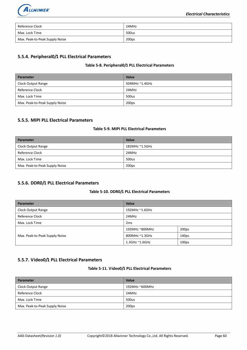
Electrical Characteristics
A40i Datasheet(Revision 1.0) Copyright© 2018 Allwinner Technology Co.,Ltd. All Rights Reserved. Page 60
Reference Clock 24MHz
Max. Lock Time 500us
Max. Peak-to-Peak Supply Noise 200ps
5.5.4. Peripheral0/1 PLL Electrical Parameters
Table 5-8. Peripheral0/1 PLL Electrical Parameters
Parameter Value
Clock Output Range 504MHz ~1.4GHz
Reference Clock 24MHz
Max. Lock Time 500us
Max. Peak-to-Peak Supply Noise 200ps
5.5.5. MIPI PLL Electrical Parameters
Table 5-9. MIPI PLL Electrical Parameters
Parameter Value
Clock Output Range 182MHz ~1.5GHz
Reference Clock 24MHz
Max. Lock Time 500us
Max. Peak-to-Peak Supply Noise 200ps
5.5.6. DDR0/1 PLL Electrical Parameters
Table 5-10. DDR0/1 PLL Electrical Parameters
Parameter Value
Clock Output Range 192MHz ~1.6GHz
Reference Clock 24MHz
Max. Lock Time 2ms
Max. Peak-to-Peak Supply Noise
192MHz ~800MHz 200ps
800MHz ~1.3GHz 140ps
1.3GHz ~1.6GHz 100ps
5.5.7. Video0/1 PLL Electrical Parameters
Table 5-11. Video0/1 PLL Electrical Parameters
Parameter Value
Clock Output Range 192MHz ~600MHz
Reference Clock 24MHz
Max. Lock Time 500us
Max. Peak-to-Peak Supply Noise 200ps
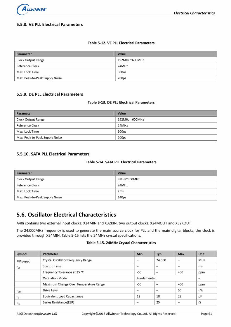
Electrical Characteristics
A40i Datasheet(Revision 1.0) Copyright© 2018 Allwinner Technology Co.,Ltd. All Rights Reserved. Page 61
5.5.8. VE PLL Electrical Parameters
Table 5-12. VE PLL Electrical Parameters
Parameter Value
Clock Output Range 192MHz ~600MHz
Reference Clock 24MHz
Max. Lock Time 500us
Max. Peak-to-Peak Supply Noise 200ps
5.5.9. DE PLL Electrical Parameters
Table 5-13. DE PLL Electrical Parameters
Parameter Value
Clock Output Range 192MHz ~600MHz
Reference Clock 24MHz
Max. Lock Time 500us
Max. Peak-to-Peak Supply Noise 200ps
5.5.10. SATA PLL Electrical Parameters
Table 5-14. SATA PLL Electrical Parameters
Parameter Value
Clock Output Range 8MHz~300MHz
Reference Clock 24MHz
Max. Lock Time 2ms
Max. Peak-to-Peak Supply Noise 140ps
5.6. Oscillator Electrical Characteristics
A40i contains two external input clocks: X24MIN and X32KIN, two output clocks: X24MOUT and X32KOUT.
The 24.000MHz frequency is used to generate the main source clock for PLL and the main digital blocks, the clock is provided through X24MIN. Table 5-15 lists the 24MHz crystal specifications.
Table 5-15. 24MHz Crystal Characteristics
Symbol Parameter Min Typ Max Unit
1/(tCPMAIN) Crystal Oscillator Frequency Range – 24.000 – MHz
tST Startup Time – – – ms
Frequency Tolerance at 25 °C -50 – +50 ppm
Oscillation Mode Fundamental –
Maximum Change Over Temperature Range -50 – +50 ppm
PON Drive Level – – 50 uW
CL Equivalent Load Capacitance 12 18 22 pF
RS Series Resistance(ESR) – 25 – Ω

Electrical Characteristics
A40i Datasheet(Revision 1.0) Copyright© 2018 Allwinner Technology Co.,Ltd. All Rights Reserved. Page 62
Duty Cycle 30 50 70 %
CI Motional Capacitance – – – pF
CO Shunt Capacitance 5 6.5 7.5 pF
RBIAS Internal Bias Resistor 0.5 0.6 0.7 MΩ
The 32768Hz frequency is used for low frequency operation. It supplies the wake-up domain for operation in lowest power mode. The clock is provided through X32KIN. Table 5-16 lists the 32768Hz crystal specifications.
Table 5-16. 32768Hz Crystal Characteristics
Symbol Parameter Min Typ Max Unit
1/(tCPMAIN) Crystal Oscillator Frequency Range – 32768 – Hz
tST Startup Time – – – ms
Frequency Tolerance at 25 °C -20 – +20 ppm
Oscillation Mode Fundamental –
Maximum Change Over Temperature Range -20 – +20 ppm
PON Drive Level – – 1.0 uW
CL Equivalent Load Capacitance – 12.5 – pF
RS Series Resistance(ESR) – – 35 kΩ
Duty Cycle 30 50 70 %
CI Motional Capacitance – – – F
CO Shunt Capacitance – 1.1 – pF
5.7. Maximum Current Consumption
If you have questions about power consumption parameters, contact Allwinner FAE.
5.8. External Memory Electrical Characteristics
5.8.1. Nand AC Electrical Characteristics
Figure 5-1. Conventional Serial Access Cycle Timing (SAM0)

Electrical Characteristics
A40i Datasheet(Revision 1.0) Copyright© 2018 Allwinner Technology Co.,Ltd. All Rights Reserved. Page 63
Figure 5-2. EDO Type Serial Access after Read Cycle Timing (SAM1)
Figure 5-3. Extending EDO Type Serial Access Mode Timing (SAM2)
Figure 5-4. Command Latch Cycle Timing

Electrical Characteristics
A40i Datasheet(Revision 1.0) Copyright© 2018 Allwinner Technology Co.,Ltd. All Rights Reserved. Page 64
Figure 5-5. Address Latch Cycle Timing
Figure 5-6. Write Data to Flash Cycle Timing
Figure 5-7. Waiting R/B# Ready Timing

Electrical Characteristics
A40i Datasheet(Revision 1.0) Copyright© 2018 Allwinner Technology Co.,Ltd. All Rights Reserved. Page 65
Figure 5-8. WE# High to RE# Low Timing
Figure 5-9. RE# High to WE# Low Timing
Figure 5-10. Address to Data Loading Timing
Table 5-17. NAND Timing Constants
Parameter Symbol Timing Unit
NDFC_CLE setup time t1 2T ns
NDFC_CLE hold time t2 2T(1) ns

Electrical Characteristics
A40i Datasheet(Revision 1.0) Copyright© 2018 Allwinner Technology Co.,Ltd. All Rights Reserved. Page 66
NDFC_CE setup time t3 2T ns
NDFC_CE hold time t4 2T ns
NDFC_WE# pulse width t5 T ns
NDFC_WE# hold time t6 T ns
NDFC_ALE setup time t7 2T ns
Data setup time t8 T ns
Data hold time t9 T ns
Ready to NDFC_RE# low t10 3T ns
NDFC_ALE hold time t11 2T ns
NDFC_RE# pulse width t12 T ns
NDFC_RE# hold time t13 T ns
Read cycle time t14 2T ns
Write cycle time t15 2T ns
NDFC_WE# high to R/B# busy t16 T_WB(2) ns
NDFC_WE# high to NDFC_RE# low t17 T_WHR(3) ns
NDFC_RE# high to NDFC_WE# low t18 T_RHW(4) ns
Address to Data Loading time t19 T_ADL(5) ns
NOTE (1):T is the cycle of clock. NOTE (2),(3),(4),(5):This values is configurable in Nand Flash controller. The value of T_WB could be 28T/44T/60T/76T, the value of T_WHR could be 0T/12T/28T/44T, the value of T_RHW could be 8T/24T/40T/56T, the value of T_ADL could be 0T/12T/28T/44T.
5.8.2. SMHC AC Electrical Characteristics
tODLY
tOSKEW
CLK
CMD, DATA
tCK
Figure 5-11. SMHC in SDR Mode Output Timing
tIDLY
tISKEW
CLK
CMD, DATA
tCK
Figure 5-12. SMHC in SDR Mode Input Timing
Table 5-18. SMHC Timing Constants
Parameter Symbol Min Type Max Unit

Electrical Characteristics
A40i Datasheet(Revision 1.0) Copyright© 2018 Allwinner Technology Co.,Ltd. All Rights Reserved. Page 67
Clock frequency tCK 0 50 50 MHz
Duty Cycle DC 45 50 55 %
CMD, Data output delay time tODLY - - 12 ns
Data output delay skew time tOSKEW - - 0.5 ns
Data input delay in SDR mode. It includes Clock’s PCB delay time, Data’s PCB delay time and device’s data output delay.
tIDLY - - 21 ns
Data input skew time in SDR mode
tISKEW - - 0.8 ns
Note (1): Output CMD, DATA is referenced to CLK.
5.9. External Peripherals Electrical Characteristics
5.9.1. LCD AC Electrical Characteristics
Vsync
LD[23..0]
Hsync
tVSPW
tVBP
tVT
Vsync
LD[23..0]
Hsync
tVSPW
tVBP
tVT
Vertical invalid data period Vertical invalid data periodDH1 DH2 DHy
1//2H
Vertical invalid data period Vertical invalid data periodDH1 DH2 DHy
Odd/Even field
Even field
Figure 5-13. HV_IF Interface Vertical Timing

Electrical Characteristics
A40i Datasheet(Revision 1.0) Copyright© 2018 Allwinner Technology Co.,Ltd. All Rights Reserved. Page 68
Hsync
LD[23..0]
DCLK
tHSPWtHBP
tHT
Invalid D1 D2 D3
LDE
tDCLK
D320
Figure 5-14. HV_IF Interface Parallel Mode Horizontal Timing
Hsync
LD[7..0]
DCLK
tHSPW
tHBPtHT
Invalid R0 G1 B2
LDE
tDCLK
B959R3
One Pixel
Figure 5-15. HV_IF Interface Serial Mode Horizontal Timing
Table 5-19. LCD HV_IF Interface Timing Constants
Parameter Symbol Min Typ Max Unit
DCLK cycle time tDCLK 5 - - ns
HSYNC period time tHT - HT+1 - tDCLK
HSYNC width tHSPW - HSPW+1 - tDCLK
HSYNC back porch tHBP - HBP+1 - tDCLK
VSYNC period time tVT - VT/2 - tHT
VSYNC width tVSPW - VSPW+1 - tHT
VSYNC back porch tVBP - VBP+1 - tHT

Electrical Characteristics
A40i Datasheet(Revision 1.0) Copyright© 2018 Allwinner Technology Co.,Ltd. All Rights Reserved. Page 69
(1). Vsync: Vertical sync, indicates one new frame (2). Hsync: Horizontal sync, indicate one new scan line (3). DCLK: Dot clock, pixel data are sync by this clock (4). LDE: LCD data enable (5). LD[23..0]: 24Bit RGB/YUV output from input FIFO for panel
5.9.2. CSI AC Electrical Characteristics
VSYNC
HSYNC
DATA
HSYNC
DATA[7/9/11:0]
PCLK
n frame n+1 frame
…
first line second line last line
…
…
…
Figure 5-16. 8/10/12-bit CMOS Sensor Interface Timing (clock rising edge sample. vsync valid = positive, hsycn valid = positive)
VSYNC
HSYNC
PCLK
D[15:8]
D[7:0]
val
val
val val
val val val val
val val
Y0[7:0]
Y1[7:0]
Y2[7:0]
Y3[7:0]
Y4[7:0]
Y5[7:0]
Y6[7:0]
...
Cb0[7:0]
Cb1[7:0]
Cb2[7:0]
Cb3[7:0]
Cr0[7:0]
Cr1[7:0]
Cr2[7:0]
...
blank blankPixel0 Pixel1 Pixel2 Pixel3 Pixel4 Pixel5 Pixel6 ...
Figure 5-17. 16-bit YCbCr4:2:2 with Separate Sync Timing (clock rising edge sample. vsync valid = positive, hsycn valid = positive)
PCLK
D[7:0]Cb0
[7:0]Y0
[7:0]Cr0
[7:0]Y1
[7:0]Cb2
[7:0]Y2
[7:0]Cr2
[7:0]...
SAV blankPixel0~Pixel1 Pixel2~Pixel3 ...
FF 00 00 XY FFY3
[7:0]
Figure 5-18. 8-bit YCbCr4:2:2 with Embedded Syncs(BT656) Timing

Electrical Characteristics
A40i Datasheet(Revision 1.0) Copyright© 2018 Allwinner Technology Co.,Ltd. All Rights Reserved. Page 70
PCLK
DATA
tperiod
tdst tdhd
thigh-level
Figure 5-19. Data Sample Timing
Table 5-20. CSI Interface Timing Constants
Parameter Symbol Min Typ Max Unit
Pclk Period tperiod 5.95 - - ns
Pclk Frequency 1/tperiod - - 168 MHz
Pclk Duty thigh-level/tperiod 40 50 60 %
Data input Setup time tdst 0.6 - - ns
Data input Hold time tdhd 0.6 - - ns
5.9.3. EMAC AC Electrical Characteristics
TX_CLK
Tch Tcl
Ts Th
TXD[3:0]TX_EN
Figure 5-20. EMAC MII Interface Transmit Timing
Table 5-21. 100Mb/s MII Transmit Timing Constants
Parameter Symbol Min Type Max Unit
Transmit Clock High Time,100M mode Tch - 20 - ns
Transmit Clock Low Time,100M mode Tcl - 20 - ns
TXEN/TXD setup time to TX_CLK Ts 10 - - ns
TXEN/TXD hold time to TX_CLK Th 0 - - ns
RX_CLK
RXD[3:0]RX_DVRX_ER
Valid Data
Tch Tcl
Td
Figure 5-21. EMAC MII Interface Receive Timing
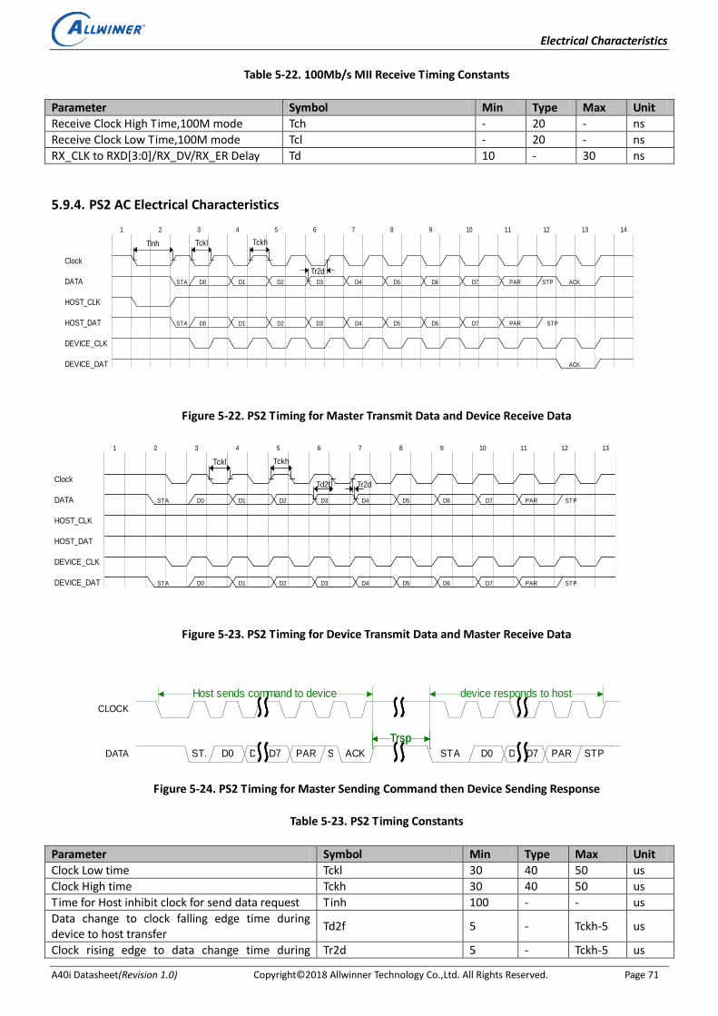
Electrical Characteristics
A40i Datasheet(Revision 1.0) Copyright© 2018 Allwinner Technology Co.,Ltd. All Rights Reserved. Page 71
Table 5-22. 100Mb/s MII Receive Timing Constants
Parameter Symbol Min Type Max Unit
Receive Clock High Time,100M mode Tch - 20 - ns
Receive Clock Low Time,100M mode Tcl - 20 - ns
RX_CLK to RXD[3:0]/RX_DV/RX_ER Delay Td 10 - 30 ns
5.9.4. PS2 AC Electrical Characteristics
1 2 3 4 5 6 7 8 9 10 11 12 13 14
STA D0 D1 D2 D3 D4 D5 D6 D7 PAR STP
Tinh Tckh
Tr2d
STA D0 D1 D2 D3 D4 D5 D6 D7 PAR STP
ACK
Tckl
ACK
Clock
DATA
HOST_CLK
HOST_DAT
DEVICE_CLK
DEVICE_DAT
Figure 5-22. PS2 Timing for Master Transmit Data and Device Receive Data
1 2 3 4 5 6 7 8 9 10 11 12 13
STA D0 D1 D2 D3 D4 D5 D6 D7 PAR STP
STPPARD7D6D5D4D3D2D1D0STA
Tckl Tckh
Td2f Tr2dClock
DATA
HOST_CLK
HOST_DAT
DEVICE_CLK
DEVICE_DAT
Figure 5-23. PS2 Timing for Device Transmit Data and Master Receive Data
STA D0 D1 D7 PAR STPACK STA D0 D1 D7 PAR STP
TrspTrsp
device responds to hostHost sends command to device
CLOCK
DATA
Figure 5-24. PS2 Timing for Master Sending Command then Device Sending Response
Table 5-23. PS2 Timing Constants
Parameter Symbol Min Type Max Unit
Clock Low time Tckl 30 40 50 us
Clock High time Tckh 30 40 50 us
Time for Host inhibit clock for send data request Tinh 100 - - us
Data change to clock falling edge time during device to host transfer
Td2f 5 - Tckh-5 us
Clock rising edge to data change time during Tr2d 5 - Tckh-5 us

Electrical Characteristics
A40i Datasheet(Revision 1.0) Copyright© 2018 Allwinner Technology Co.,Ltd. All Rights Reserved. Page 72
device to host transfer
Data change to clock rising edge time during host to device transfer
Td2r 5 - Tckl-5 us
Clock falling edge to data change time during host to device transfer
Tf2d 5 - Tckl-5 us
Host pull low Clock to Device drive Clock Tc2c - - 15 ms
Time for packet to send Tdata - - 2 ms
Time for device responding to the host command Trsp - - 20 ms
5.9.5. CIR AC Electrical Characteristics
Tlh Tll Tp T0T1
Address #Address Command #Command
Tf
IR_NEC
Figure 5-25. CIR-RX Timing
Table 5-24. CIR-RX Timing Constants
Parameter Symbol Min Type Max Unit
Frame Period Tf - 67.5 - ms
Lead Code High Time Tlh - 9 - ms
Lead Code Low Time Tll - 4.5 - ms
Pulse Time Tp - 560 - us
Logical 1 Low Time T1 - 1680 - us
Logical 0 Low Time T0 - 560 - us
5.9.6. SPI AC Electrical Characteristics
Figure 5-26. SPI MOSI Timing

Electrical Characteristics
A40i Datasheet(Revision 1.0) Copyright© 2018 Allwinner Technology Co.,Ltd. All Rights Reserved. Page 73
Figure 5-27. SPI MISO Timing
Table 5-25. SPI Timing Constants
Parameter Symbol Min Typ Max Unit
CS# Active Setup Time tSLCH - 2T - ns
CS# Active Hold Time tCHSH - 2T(1) - ns
Data In Setup Time tDVCH - T/2-3 - ns
Data In Hold Time tCHDX - T/2-3 - ns
Note (1):T is the cycle of clock.
5.9.7. UART AC Electrical Characteristics
start data parity stop
vaild data
tRXSF
RX
RX FIFO DATA
Register Setting:
Data length(DLS in LCR[1:0]) = 3 (8bit)
Stop bit length(STOP in LCR[2]) = 1 (2bit)
Parity enable(PEN in LCR[3]) = 1
Figure 5-28. UART RX Timing
data parity stop TX
nCTS
start
tDCTS tACTS
start
Figure 5-29. UART nCTS Timing

Electrical Characteristics
A40i Datasheet(Revision 1.0) Copyright© 2018 Allwinner Technology Co.,Ltd. All Rights Reserved. Page 74
FD -3
tDRTS tARTS
RX FIFO DATA NUM
nRTS
FD-2 0
Register Setting:
RTS Trigger level(RT in FCR[7:6]) = 3 (De-asserted nRTS when FIFO valid data number reach FIFO depth-2)
(1)
Note (1): FD: FIFO Depth
Figure 5-30. UART nRTS Timing
Table 5-26. UART Timing Constants
Parameter Symbol Min Typ Max Unit
RX start to RX FIFO tRXSF 10.5× BRP(1) - 11× BRP(1) ns
Delay time of de-asserted nCTS to TX start
tDCTS - - BRP(1) ns
Step time of asserted nCTS to stop next transmission
tACTS BRP(1)/4 - - ns
Delay time of de-asserted nRTS
tDRTS - - BRP(1) ns
Delay time of asserted nRTS tARTS - - BRP(1) ns
Note (1): BRP(Baud-Rate Period).
5.9.8. TWI AC Electrical Characteristics
tSTH
SDA
SCL
tCL tSOS
tDHtDS
tCH
Figure 5-31. TWI Timing
Table 5-27. TWI Timing Constants
Parameter Symbol Min Typ Max Unit
High period of SCL tCH 0.96 - - μs
Low period of SCL tCL 1.5 - - μs
SCL hold time for START condition
tSTH 1.5 - - μs
SCL step time for STOP condition
tSOS 1.6 - - μs
SDA hold time tDH 0.82 - - μs
SDA step time tDS 0.72 - - μs

Electrical Characteristics
A40i Datasheet(Revision 1.0) Copyright© 2018 Allwinner Technology Co.,Ltd. All Rights Reserved. Page 75
5.9.9. TSC AC Electrical Characteristics
Data
Clock
T1
T2
T
Figure 5-32. TSC Data and Clock Timing
Table 5-28. TSC Timing Constants
Parameter Symbol Min Type Max Unit
Data hold time T1 T/2-T/10 T(1)/2 T/2+T/10 us
Clock pulse width T2 T/2-T/10 T/2 T/2+T/10 us
Note (1):T is the cycle of clock.
5.9.10. AC97 AC Electrical Characteristics
RESET#
BIT_CLK
SDATA_IN
Trst_low
Ttri2actv
Ttri2actv
Ttri2actv
Figure 5-33. AC97 Cold Reset Timing
RESET#
BIT_CLK
Tsync_high
Tsync2clk
Figure 5-34. AC97 Warm Reset Timing
SYNC
BIT_CLK
SDATA_OUT
SDATA_IN
Slot 1 Slot 2
Write to 0x26 Data PR4
Ts2_pdown
Note: BIT_CLK not to scale

Electrical Characteristics
A40i Datasheet(Revision 1.0) Copyright© 2018 Allwinner Technology Co.,Ltd. All Rights Reserved. Page 76
Figure 5-35. AC-link Low Power Mode Timing
BIT_CLK
Tclk_low
Tclk_high
Tclk_period
SYNC
Tsync_low
Tsync_high
Tsync_period
Figure 5-36. BIT_CLK and SYNC Timing
BIT_CLK
SDATA_OUTSDATA_IN
SYNC
Voh
Vol
Vih
Vil
tco tsetup
thold
Figure 5-37. AC-link Data Transmission Output and Input Timing
BIT_CLK
Triseclk Tfallclk
SYNC
Trisesync Tfallsync
SDATA_IN
Trisedin Tfalldin
SDATA_OUT
Trisedout Tfalldout
Figure 5-38. Signal Rise and Fall Timing
Table 5-29. AC97 Timing Constants
Parameter Symbol Min Type Max Unit

Electrical Characteristics
A40i Datasheet(Revision 1.0) Copyright© 2018 Allwinner Technology Co.,Ltd. All Rights Reserved. Page 77
RESET# active low pulse width Trst_low 1.0 - - us
RESET# inactive to SDATA_IN Or BIT_CLK active delay
Ttri2actv - - 25 ns
RESET# inactive to BIT_CLK Startup delay
Trst2clk 162.8 - - ns
SYNC active high pulse width Tsync_high 1.0 - - us
SYNC inactive to BIT_CLK startup delay
Tsync2clk 162.8 - - ns
End of Slot 2 to BIT_CLK, SDATA_IN low
Ts2_pdown - - 1.0 us
BIT_CLK frequency - 12.288 - MHz
BIT_CLK period Tclk_period - 81.4 - ns
BIT_CLK output jitter - - 750 ps
BIT_CLK high pulse width Tclk_high 36 40.7 45 ns
BIT_CLK low pulse width Tclk_low 36 40.7 45 ns
SYNC frequency - 48.0 - kHz
SYNC period Tsync_period - 20.8 - us
SYNC high pulse width Tsync_high - 1.3 - us
SYNC low pulse width Tsync_low - 19.5 - us
Output Valid Delay from rising edge of BIT_CLK
tco - - 15 ns
Input Setup to falling edge of BIT_CLK tsetup 10 - - ns
Input Hold from falling edge of BIT_CLK
thold 10 - - ns
BIT_CLK combined rise or fall plus flight time (Primary Codec to Controller or Secondary)
- - 7 ns
SDATA combined rise or fall plus flight time (Output to Input)
- - 7 ns
BIT_CLK rise time Triseclk - - 6 ns
BIT_CLK fall time Tfallclk - - 6 ns
SYNC rise time Trisesync - - 6 ns
SYNC fall time Tfallsync - - 6 ns
SDATA_IN rise time Trisedin - - 6 ns
SDATA_IN fall time Tfalldin - - 6 ns
SDATA_OUT rise time Trisedout - - 6 ns
SDATA_OUT fall time Tfalldout - - 6 ns
(1). Worst case duty cycle restricted to 45/55 (2). Combined rise or fall plus flight times are provided for worst case scenario modeling purpose (3). BIT_CLK rise/fall times with an external load of 75 pF (4). SYNC and SDATA_OUT rise/fall times with a external load of 75 pF (5). SDATA_IN rise/fall times with an external load of 60 pF (6). Rise is from 10% to 90% of Vdd (Vol to Voh) (7). Fall is from 90% to 10% of Vdd (Voh to Vol)

Electrical Characteristics
A40i Datasheet(Revision 1.0) Copyright© 2018 Allwinner Technology Co.,Ltd. All Rights Reserved. Page 78
5.9.11. SCR AC Electrical Characteristics
Undefined
I/O
CLK
tb
tc
RST
VCC
ta
Card Answer
T1 T2 T3
Figure 5-39. SCR Activation and Cold Reset Timing
Undefined
I/O
CLK
te
tf
RST
VCC
tdCard Answer
T4 T5
Figure 5-40. SCR Warm Reset Timing
Table 5-30. SCR Timing Constants
Symbol Min Type Max Unit
ta - - 200/f us
tb 400/f - - us
tc 400/f - 40000/f us
td - - 200/f us
te 400/f - - us
tf 400/f - 40000/f us
(1). Activation: Before time T1 (2). Cold Reset: After time T1 (3). T1: The clock signal is applied to CLK at time T1. (4). T2: The RST is put to state H. (5). T3: The card begin answer at time T3 (6). ta: The card shall set I/O to state H within 200 clock cycles (delay ta) after the clock signal is applied to CLK (at time T1+ta). (7). tb: The cold reset results from maintaining RST at state L for at least 400 clock cycles (delay tb) after the clock signal is applied to CLK (at time T1+tb). (8). tc: The answer on I/O shall begin between 400 and 40000 clock cycles (delay tc) after the rising edge of the signal on RST (at time T2+tc). (9). td: The card shall set I/O to state H within 200 clock cycles (delay td) after state L is applied to RST (at time T4+td). (10). te: The controller initiates a warm reset (at time T4) by putting RST to state L for at least 400 clock cycles (delay te) while VCC remains powered and CLK provided with a suitable and stabled clock signal.

Electrical Characteristics
A40i Datasheet(Revision 1.0) Copyright© 2018 Allwinner Technology Co.,Ltd. All Rights Reserved. Page 79
(11). tf: The card answer on I/O shall begin between 400 and 40000 clock cycles (delay tf) after the rising edge of the signal on RST (at time T5+tf). (12). f is the frequency of clock.
5.10. Power-up and Power-down Sequence
The following figure shows an example of the power-up sequence for A40i device. During the entire power-up sequence, the AP_RESET# pin must be held on low until all power domains are stable. The other power domains not in Figure 5-41 can be turned on upon the software request.
Figure 5-41. A40i Power Up Sequence
The power down solution is achieved by setting AP_RESET# to 0. When AP_RESET# powered down, then all power supplies start ramp down except VCC_RTC. The ramping down rate is decided by the load on the power supply.

Package Thermal Characteristics
A40i Datasheet(Revision 1.0) Copyright© 2018 Allwinner Technology Co.,Ltd. All Rights Reserved. Page 80
6. Package Thermal Characteristics
Table 6-1 shows thermal resistance parameters of the A40i. The following thermal resistance characteristics in Table 6-1 is based on JEDEC JESD51 standard, because the actual system design and temperature could be different with JEDEC JESD51 , the simulating result data is a reference only, please prevail in the actual application condition test.
NOTE Test condition: four-layer board(2s2p),natural convection, no air flow.
Table 6-1. A40i Thermal Resistance Characteristics
Symbol Parameter Min Typ Max Unit
θ JA Junction-to-Ambient Thermal Resistance - 24 - °C/W
θ JB Junction-to-Board Thermal Resistance - TBD - °C/W
θ JC Junction-to-Case Thermal Resistance - TBD - °C/W
(1). °C/W : degrees Celsius per watt.

Pin Assignment
A40i Datasheet(Revision 1.0) Copyright© 2018 Allwinner Technology Co.,Ltd. All Rights Reserved. Page 81
7. Pin Assignment
7.1. Pin Map
For A40i, FBGA 468 balls ,16 x 16 mm, 0.65 pitch package is offered. The pin maps are illustrated in Figure 7-1 for this package.
Figure 7-1. A40i Pin Map

Pin Assignment
A40i Datasheet(Revision 1.0) Copyright© 2018 Allwinner Technology Co.,Ltd. All Rights Reserved. Page 82
7.2. Package Dimension
Figure 7-2 shows the top, bottom, and side views of A40i package dimension.
Figure 7-2. A40i Package Dimension

A40i Datasheet(Revision 1.0) Copyright© 2018 Allwinner Technology Co.,Ltd. All Rights Reserved. Page 83
Copyright © 2018 Allwinner Technology Co.,Ltd. All Rights Reserved. Allwinner Technology Co.,Ltd. No.9 Technology Road 2,High-Tech Zone, Zhuhai, Guangdong Province, China Contact US: [email protected] www.allwinnertech.com