Embed Size (px)
Citation preview

1
A wireless 802.11 condition monitoring sensor for
electrical substation environments
By
Alexander Clive Bogias
A thesis submitted in partial fulfillment of the requirements for the
degree of
Doctor of Philosophy
2012
School of Engineering
Cardiff University

i
Abstract
The work reported in this thesis is concerned with the design, development and
testing of a wireless 802.11 condition monitoring sensor for an electrical substation
environments. The work includes a comprehensive literature review and the design and
development of a novel continuous wireless data acquisition sensor. Laboratory and
field tests were performed to evaluate the data acquisition performance of the developed
wireless sensor. The sensor‟s wireless immunity to interference performance was also
evaluated in laboratory and field tests.
The literature survey reviews current condition monitoring practices in electrical
substation environments with a focus on monitoring high voltage insulators and
substation earth impedance.
The data acquisition performance of the wireless sensor was tested in a
laboratory using two artificially polluted insulators, in a fog chamber that applied clean
fog. Analysis of the test results were found to be in good agreement with those recorded
directly through a data acquisition card and transmitted via coaxial cable. The wireless
impedance measurement of a 275kV transmission earth tower base field test was also
performed and was found to be in agreement with previous published results from
standard earth measurements.
The sensor‟s wireless interference performance was evaluated at a field test site
when no high voltage experiments were taking place. The sensors wireless interference
performance was then tested in a laboratory environment before and during high voltage
tests taking place. The results of these tests were compared to each other and to
published results. These tests demonstrate the suitability of the sensor‟s design and its
immunity to interference.
The experimental work conducted using the developed wireless sensor has led to
an understanding that continuous wireless data acquisition is possible in high voltage
environments. However, novel condition monitoring systems that make use of such
wireless sensors, have to take into account data losses and delays adequately.
Furthermore, a solar power source was designed and constructed to be used for
outdoor substation applications and the solar battery charging performance of the
wireless sensor was tested in a solar laboratory.

ii
DECLARATION
This work has not previously been accepted in substance for any degree and is not
concurrently submitted in candidature for any degree.
Signed ______________________ (candidate) Date___________________
STATEMENT 1
This thesis is being submitted in partial fulfilment of the requirements for the degree of
PhD.
Signed______________________ (candidate) Date___________________
STATEMENT 2
This thesis is the result of my own independent work/investigation, except where
otherwise stated. Other sources are acknowledged by explicit references.
Signed______________________ (candidate) Date___________________
STATEMENT 3
I hereby give consent for my thesis, if accepted, to be available for photocopying and
for inter-library loan, and for the title and summary to be made available to outside
organisations.
Signed______________________ (candidate) Date___________________

iii
Acknowledgements
My sincere gratitude goes to my supervisors Dr. Noureddine Harid and Prof.
Manu Haddad. Were it not for their encouragement, the many technical and other
difficulties would not have been overcome. I got the gift of knowledge and the chance
to learn from them. And while this work has taken much longer than expected, I would
like to remind everyone, including myself, that if we knew what it was we were doing,
it would not be called research, would it?
I would also like to thank the Engineering and Physical Sciences Research
Council, without whose funding none of the work would have take place. Thanks also
goes to Metageek LLC. for their donation of the Chanalyzer Pro software license and
Riverbed Technology for their donation of the Cascade Pilot software license.
Thanks also goes to Dongsheng Guo, Panos Charalampidis, David Clark,
Abdelbaset Nekeb, Salah Mousa, Mohammed Ahmeda, Fabian Moore, Nasos
Dimopoulos, Maurizio Albano, Saufi Kamarudin and Fahmi Hussin for their help,
encouragement and many fruitful discussions.
Many thanks also go to Den Slade and Paul Farugia at the electronic workshop
for their help and discussions on everything electronic and all the staff in the
engineering research office. These often unseen staff at Cardiff University helped make
my experience here a pleasant one.
A very special thank you goes to my father Fotis, my brother Chris and my late
mother Julia, without whose constant moral and emotional support none of this would
be possible. I would like to finish by dedicating this work to them.

iv
Table of Contents
List of Figures…………………………………………………………………………viii
List of Tables…………………………………………………………………………..xiv
List of Acronyms……………………………………………………………………….xv
Chapter 1 Introduction ...................................................................................................... 1
1.1 Introduction ............................................................................................................. 1
1.2 Justification for research ......................................................................................... 3
1.3 Contribution of research work ................................................................................ 5
1.4 Thesis overview ...................................................................................................... 5
Chapter 2 Overview of on-line condition monitoring and its application to outdoor
insulators and earthing systems ......................................................................................... 7
2.1 Introduction ............................................................................................................. 7
2.2 Substations .............................................................................................................. 7
2.3 On-line condition monitoring in electrical substation environments ...................... 8
2.4 Condition monitoring communication service requirements for electrical
substations ................................................................................................................... 10
2.5 Applicability of wireless sensor networks in on-line condition monitoring of
electrical substations ................................................................................................... 12
2.6 Substation assets ................................................................................................... 17
2.6.1 Introduction .................................................................................................... 17
2.6.2 Insulator pollution monitoring ....................................................................... 18
2.7 Summary ............................................................................................................... 26
Chapter 3 Wireless sensor technologies in electrical substation environments .............. 27
3.1 Wireless sensor design and components ............................................................... 27
3.1.1 Introduction .................................................................................................... 27
3.1.2 Wireless sensor components .......................................................................... 27
3.2 Key wireless sensor properties .............................................................................. 28
3.2.1 Communication .............................................................................................. 28
3.2.2 Synchronization.............................................................................................. 30
3.2.3 Sampling and processing................................................................................ 30
3.2.4 Lifespan and Energy Harvesting .................................................................... 31
3.3 Wireless network standards .................................................................................. 33
3.3.1 IEEE 802.11 a/b/g/n wireless networks ......................................................... 33

v
3.3.2 IEEE 802.15.4 wireless networks .................................................................. 39
3.3.3 IEEE 802.15.1 (Bluetooth) wireless networks ............................................... 41
3.3.4 Second, third and fourth generation cellular networks .................................. 41
3.3.5 IEEE 802.16 d/e (WiMAX) ........................................................................... 44
3.3.5 Other notable wireless CM systems ............................................................... 44
3.4 Conclusion ............................................................................................................ 45
Chapter 4 Design, development and functional testing of the WLAN sensor and its
components ..................................................................................................................... 47
4.1 Introduction ........................................................................................................... 47
4.2 The Lantronix Matchport IEEE 802.11b/g wireless module ................................ 50
4.3 Operation of the PIC24HJ256GP210 microcontroller .......................................... 51
4.3.1 Introduction .................................................................................................... 51
4.3.2 Interrupts and timers ...................................................................................... 51
4.3.3 Serial peripheral interface .............................................................................. 52
4.3.4 Universal asynchronous receiver transmitter (UART) .................................. 53
4.3.5 Input/Output ports .......................................................................................... 54
4.4 Parallel memory .................................................................................................... 55
4.5 Surge protection and anti-aliasing filters .............................................................. 55
4.5.1 Surge protection ............................................................................................. 55
4.5.2 Chopper stabilized operational amplifiers ..................................................... 59
4.6 Analog-to-digital converters ................................................................................. 64
4.7 Switching voltage regulators ................................................................................. 65
4.7.1 Introduction .................................................................................................... 65
4.7.2 Step down switching regulator ....................................................................... 66
4.7.3 Switched-Capacitor Voltage Converters ........................................................ 67
4.8 Solar powered lithium ion battery charger ............................................................ 69
4.8.1 Description of the solar powered battery charger .......................................... 69
4.8.2 Solar laboratory test arrangement .................................................................. 72
4.8.3 Test Results .................................................................................................... 73
4.9 Printed circuit board design and manufacture ....................................................... 75
4.10 Conclusion .......................................................................................................... 77
Chapter 5 Development of the firmware and software code for the WLAN sensor
operation .......................................................................................................................... 78
5.1 Introduction ........................................................................................................... 78
5.2 The microcontroller code for the wireless communication sensor ....................... 79

vi
5.3 Development of the PC-based wireless receiver code .......................................... 84
5.3.1 LabVIEW programming language ................................................................. 84
5.4 Development of the PC-based data acquisition code ............................................ 84
5.4.1 DAQ card and wireless data acquisition and processing code ....................... 84
5.4.2 Wireless data acquisition and processing code .............................................. 87
5.4.3 LabVIEW functions used for data processing ............................................... 90
5.5 Conclusion ............................................................................................................ 92
Chapter 6 Laboratory and field data acquisition trials of the developed wireless sensor
system: Application to polluted insulators and earth impedance measurements ............ 93
6.1 Introduction ........................................................................................................... 93
6.2 Laboratory test arrangement ................................................................................. 94
6.2.1 Porcelain insulator .......................................................................................... 94
6.2.2 Fog Chamber .................................................................................................. 95
6.2.3 Test circuit ...................................................................................................... 96
6.2.4 Data Acquisition Card .................................................................................... 97
6.2.5 DI-524 access point settings........................................................................... 98
6.3.4 Laboratory test procedure .................................................................................. 99
6.3.4.1 Composition of the contaminating suspension ........................................... 99
6.3.4.2 Application of the pollution layer ............................................................. 100
6.3.4.3 High-voltage test procedure ...................................................................... 100
6.4 Test results .......................................................................................................... 101
6.4.1 Porcelain insulator test ................................................................................. 101
6.4.2 Chipped porcelain test .................................................................................. 110
6.4.3 Analysis of results ........................................................................................ 118
6.5 Wireless impedance measurement field test ....................................................... 119
6.5.1 Impedance measurement system .................................................................. 119
6.5.2 Field test arrangement .................................................................................. 121
5.5.3 Test results ................................................................................................... 124
6.5.4 Analysis of results ........................................................................................ 134
6.6 Conclusions ......................................................................................................... 134
Chapter 7 Interference performance of the developed wireless sensor under laboratory
and field test conditions ................................................................................................ 135
7.1 Introduction ......................................................................................................... 135
7.2 Interference performance tests at the Llanrumney test site ................................. 136
7.2.1 Llanrumney field test equipment and software ............................................ 136

vii
7.2.2 Llanrumney field test arrangement .............................................................. 136
7.2.3 Llanrumney field test procedure .................................................................. 138
7.2.4 Llanrumney field test results ........................................................................ 139
7.3 Interference performance test in the high voltage laboratory environment ........ 147
7.3.1 High voltage laboratory test equipment and software .................................. 147
7.3.2 High voltage laboratory test arrangement .................................................... 147
7.3.3 High voltage laboratory test procedure ........................................................ 148
7.3.4 High voltage laboratory interference test results ......................................... 149
7.4 High voltage laboratory fog chamber tests ......................................................... 154
7.4.1 High voltage laboratory test equipment and software .................................. 154
7.4.2 High voltage laboratory test arrangement .................................................... 154
7.4.3 High voltage laboratory test procedure ........................................................ 154
7.4.4 High voltage laboratory test results.............................................................. 155
7.5 Analysis of results ............................................................................................... 160
7.6 Conclusion .......................................................................................................... 161
Chapter 8 General conclusions and future work ........................................................... 162
8.1 General conclusions ............................................................................................ 162
8.2 Future work ......................................................................................................... 165
8.2.1 Hardware and software improvements to wireless CM systems ................. 165
8.2.2 Substation field trials using the 802.11 wireless sensor ............................... 166
References ................................................................................................................. 168
Addendum………………………………………………………………………….....177
Appendix A ................................................................................................................. 1788
Appendix B ................................................................................................................... 188
Appendix C ................................................................................................................... 192

viii
List of Figures
Figure 2.1: An example of an air insulated substation. Reproduced from [5]. ................. 8
Figure 2.2: Survey results on benefits of using 802.11 networks to access IEDs in
substations. Reproduced from [18]. ................................................................................ 14
Figure 2.3: Results of survey on application of CM to new equipment. Reproduced from
[4]. ................................................................................................................................... 15
Figure 2.4: Results of survey on application of CM to existing equipment. Reproduced
from [4]. .......................................................................................................................... 16
Figure 2.5: A schematic impression of the relationship between leakage current and the
pollution severity as determined through laboratory testing. Reproduced from [24]. .... 19
Figure 2.6: Schematic history of polluted ceramic insulators. Reproduced from [23]. .. 20
Figure 2.7: Simplified diagram of the IPM system. Reproduced from [26]. .................. 21
Figure 2.8: Showing OLCA acquisition and processing unit, leakage current and
weather sensors. Reproduced from [27].......................................................................... 22
Figure 2.9: Backscatter leakage current monitor installation on a substation insulator.
Reproduced from [24]. .................................................................................................... 23
Figure 2.10: Impedance measurement of an earthing system. Reproduced from [36]. .. 25
Figure 3.1: Basic components of a wireless sensor......................................................... 28
Figure 3.2: Star (a) and mesh (b) topologies for wireless data communication. ............ 29
Figure 3.3: Simplified example of varying power consumption over time for a wireless
sensor. ............................................................................................................................. 32 Figure 3.4: Graphical representation of 802.11 channels in 2.4 GHz band. Reproduced
from [65]. ........................................................................................................................ 35
Figure 3.5: Use of 802.11 wireless networks for electric power systems applications.
Reproduced from [18]. .................................................................................................... 38
Figure 3.6: Use of 802.11 wireless networks for general applications by electric power
utilities. Reproduced from [18]. ...................................................................................... 38
Figure 4.1: WLAN sensor block diagram. ...................................................................... 48
Figure 4.2: Matchport b/g - Embedded Wireless Device. Reproduced from [107]. ....... 50
Figure 4.3: SPI port linking the ADC to the microcontroller. ........................................ 52
Figure 4.4: UART port linking the 802.11 module to the microcontroller. .................... 53
Figure 4.5: Microcontroller digital output port controlling power to the 802.11 module
via a MOSFET. ............................................................................................................... 54
Figure 4.6: Microcontroller digital output pin controlling power to the MCP1253-33x50
charge pump. ................................................................................................................... 54
Figure 4.7: Parallel memory operation controlled through microcontroller digital I/O
pins. ................................................................................................................................. 55
Figure 4.8: Block diagram of impulse generator test. ..................................................... 57

ix
Figure 4.9: Measured impulse voltage and current applied to the wireless sensor through
a 47 Ω resistor. ................................................................................................................ 58
Figure 4.10: Measured impulse voltage after surge protection components. ................. 59
Figure 4.11: Key filter parameters. Reproduced from [111]. ......................................... 60
Figure 4.12: Sallen-Key low pass filter. ......................................................................... 60
Figure 4.13: Butterworth amplitude response against frequency. Reproduced from
[111]. ............................................................................................................................... 61
Figure 4.14: Buffering op-amp and 6th
order Butterworth filter. .................................... 63
Figure 4.15: Measured Butterworth filter amplitude response against frequency curves.
......................................................................................................................................... 63
Figure 4.16: Functional block diagram of AD7367-5, Reproduced from [112]. ............ 64
Figure 4.17: Block diagram showing supply voltages across the wireless sensor. ......... 65
Figure 4.18: Conceptual Feedback Controlled Step-Down Regulator. Reproduced from
[113]. ............................................................................................................................... 66
Figure 4.19: Waveform showing the +3.3V supply measured at the output from the
LT1933 regulator. ........................................................................................................... 67
Figure 4.20: Simplified circuit diagram of a switched capacitor. Reproduced from [114].
......................................................................................................................................... 68
Figure 4.21: Waveforms showing the +5 V (a) and -5 V(b) supplies measured at the
outputs of the MCP1253 and TC1121 regulators. .......................................................... 69
Figure 4.22: I-V and power curves for a solar panel. Curves in red colour show the
output power from the panel for a number of irradiance magnitudes (in W/m2).
Reproduced from [115]. .................................................................................................. 70
Figure 4.23: Block diagram showing power flow from solar panel, through the LT3652
and into the batteries and voltage regulator. ................................................................... 71 Figure 4.24:Test diagram for solar battery charging test. ............................................... 72
Figure 4.25: Halogen-tube array solar test facility at Cardiff University. ...................... 73
Figure 4.26: Measure solar panel voltage and current profiles. ...................................... 74
Figure 4.27: Measured lithium-ion batteries voltage and current profiles. ..................... 74
Figure 4.28: Lithium-ion battery charging profile. Reproduced from [53]. ................... 75
Figure 4.29: Photograph of the WLAN sensor with its lithium ion batteries, aluminium
enclosure and solar panel. ............................................................................................... 77
Figure 5.1: Schematic diagram for debugging and programming of the microcontroller.
Adapted from [118]. ........................................................................................................ 79
Figure 5.2: Flowcharts showing (a) the microcontrollers main loop and (b) Tx UART
interrupt service routine. ................................................................................................. 80
Figure 5.3: Flowchart showing the microcontrollers Rx UART interrupt service routine.
......................................................................................................................................... 81
Figure 5.4: Flowcharts showing (a) the microcontrollers TIMER 3 ISR and (b) TIMER
7 ISR. .............................................................................................................................. 82
Figure 5.5: Flowchart showing the microcontrollers INT1 ISR. .................................... 83

x
Figure 5.6: Flowchart of (a) data acquisition, (b) general data processing and (c)
absolute peak leakage current data processing LabVIEW programs. ............................. 86
Figure 5.7: Flowchart of FFT data processing LabVIEW program. ............................... 87
Figure 5.8: Flowchart of wireless data acquisition LabVIEW program ......................... 89
Figure 6.1: Healthy and damaged porcelain test insulators. ........................................... 95
Figure 6.2: Fog chamber test arrangement for polluted insulator ................................... 96
Figure 6.3: High voltage test circuit. ............................................................................... 97
Figure 6.4: D-Link DI-524 wireless access point and router. Image reproduced from
[121]. ............................................................................................................................... 98
Figure 6.5: Leakage Current waveforms of healthy polluted insulator. ....................... 101
Figure 6.6: Coinciding Leakage Current waveforms of healthy polluted insulator with
the delay time of the WLAN Sensor suppressed. ......................................................... 102
Figure 6.7: Leakage Current waveforms of healthy polluted insulator. ....................... 103
Figure 6.8: Coinciding Leakage Current waveforms of healthy polluted insulator, with
the lead time of the WLAN Sensor suppressed. ........................................................... 104
Figure 6.9: Operating voltage and leakage current of a healthy polluted insulator. ..... 105
Figure 6.10: FFT of leakage current showing a frequency window of 0-1000Hz. ....... 105
Figure 6.11: FFT of operating voltage showing a frequency window of 0-1000Hz..... 105
Figure 6.12: Operating voltage and leakage current of a healthy polluted insulator with
surface discharges. ........................................................................................................ 106
Figure 6.13: Operating voltage and leakage current of a healthy polluted insulator with
surface discharges. ........................................................................................................ 107
Figure 6.14: FFT of leakage current showing a frequency window of 0-1000Hz.. ...... 107
Figure 6.15: FFT of leakage current showing a frequency window of 0-1000Hz.. ...... 107 Figure 6.16: Operating voltage and leakage current characteristics for a healthy polluted
insulator measured using the WLAN sensor. ................................................................ 109
Figure 6.17: Leakage Current waveforms of chipped polluted insulator...................... 110
Figure 6.18: Leakage Current waveforms of chipped polluted insulator with the delay
time of the WLAN Sensor suppressed. ......................................................................... 111
Figure 6.19: Leakage Current waveforms of chipped polluted insulator..................... 112
Figure 6.20: Leakage Current waveforms of chipped polluted insulator, with the lead
time of the WLAN Sensor suppressed. ......................................................................... 113
Figure 6.21: Operating voltage and leakage current of a chipped polluted insulator. .. 114
Figure 6.22: FFT of leakage current showing a frequency window of 0-1000Hz. ....... 114
Figure 6.23: FFT of operating voltage showing a frequency window of 0-1000Hz..... 114
Figure 6.24: Operating voltage and leakage current of a chipped polluted insulator. .. 115
Figure 6.25: FFT of leakage current showing a frequency window of 0-1000Hz. ....... 115
Figure 6.26: FFT of operating voltage showing a frequency window of 0-1000Hz..... 116
Figure 6.27: Operating voltage and leakage current characteristics for a chipped polluted
insulator measured using the WLAN sensor. ................................................................ 117

xi
Figure 6.28: Circuit Configuration used for the IMS system and WLAN sensor......... 120
Figure 6.29: Lock-in amplifiers and power amplifier of the IMS. ............................... 120
Figure 6.30: Voltage and current transducers used for the IMS system. ...................... 121
Figure 6.31: Satellite image showing Llanrumney test site. (A): Remote computer and
802.11 access point, (B): IMS and WLAN Sensor location, (C): Reference voltage
electrode location, (D): Current return earth rod location. Image reproduced from
Google Maps©. ............................................................................................................. 122
Figure 6.32: Block diagram of IMS test at the Llanrumney test field. ......................... 123
Figure 6.33: 10dBi Directional 2.4GHz antenna. ......................................................... 123
Figure 6.34: EPR and injected current for the tower base earth impedance measurement.
....................................................................................................................................... 124
Figure 6.35: FFTs of the EPR and injected current. ..................................................... 125
Figure 6.36: EPR and injected current for the tower base earth impedance measurement.
Tower leg four disconnected. ........................................................................................ 126
Figure 6.37: FFTs of the EPR and injected current when tower leg four was
disconnected. ................................................................................................................. 127
Figure 6.38: EPR and injected current characteristics for the tower base earth impedance
measurement. ................................................................................................................ 128
Figure 6.39: EPR and injected current for the tower base earth impedance measurement.
....................................................................................................................................... 129
Figure 6.40: FFTs of the EPR and injected current for the tower base earth impedance
measurement. ................................................................................................................ 130
Figure 6.41: EPR and injected current for the tower base earth impedance measurement.
Tower legs three and four disconnected........................................................................ 131
Figure 6.42: FFTs of the EPR and injected current when tower legs three and four were
disconnected. ................................................................................................................. 132
Figure 6.43: EPR and injected current characteristics for the tower base earth impedance
measurement. ................................................................................................................ 133
Figure 7.1: Satellite image showing Llanrumney test site. Image reproduced from
Google Maps©. ............................................................................................................. 137
Figure 7.2: Llanrumney test site equipment configuration ........................................... 138
Figure 7.3: Waterfall view for channel 1 test. Colours represent power levels in the
spectrum with dark blue as low and bright red as higher amplitude levels. ................. 140
Figure 7.4: Normal traffic vs. retransmissions between DI-524 and WLAN Sensor ... 144
Figure 7.5: Total bits transmitted with respect to transmission frame rate ................... 146
Figure 7.6: High voltage laboratory floor plan. Not to scale. ....................................... 148
Figure 7.7: Normal traffic vs. retransmissions between DI-524 and WLAN Sensor on
channel 1 ....................................................................................................................... 152
Figure 7.8: Total bits transmitted with respect to transmission frame rate ................... 153
Figure 7.9: Normal traffic vs. retransmissions between DI-524 and WLAN Sensor ... 158
Figure 7.10: Total bits transmitted with respect to transmission frame rate ................. 159

xii
Figure A.1: Channel 0 - Surge protection and active low-pass filter circuit
schematic……………………………………………………………………………...178
Figure A.2: Channel 1 - Surge protection and active low-pass filter circuit
schematic……………………………………………………………………………...179
Figure A.3: Microcontroller circuit schematic………………………………………..180
Figure A.4: WLAN connectors and parallel memory circuit schematic……………...181
Figure A.5: Bipolar ADC circuit schematic…………………………………………..182
Figure A.6: Step-down (+3.3V), Step-up (+5V) and Inverting (-5V) regulators circuit
schematic…………………………………………………………………………...…183
Figure A.7: Solar powered battery charger circuit schematic………………………...184
Figure B.1: Peak leakage current characteristic for the healthy polluted insulator…...188
Figure B.2: Operating voltage and leakage current characteristics for a healthy polluted
insulator measured using the DAQ card……………………………………………...189
Figure B.3: Peak leakage current characteristic for the damaged polluted insulator…190
Figure B.4: Operating voltage and leakage current characteristics for a healthy polluted
insulator measured using the DAQ card……………………………………………...191
Figure C.1: Waterfall view showing 1 minute of 2.4-2.5GHz spectrum measurements
- Llanrumney test field…………………………………………………………….....193
Figure C.2: Density View showing 1 minute of 2.4-2.5GHz spectrum measurements
- Llanrumney test field………………………………………………………………..193
Figure C.3: Signal strength of DI-524 access point measured at WLAN Sensor -
Llanrumney field test………………………………………………………………....194
Figure C.4: Waterfall view of 2.4-2.5GHz spectrum - Llanrumney field test………..195
Figure C.5: Signal strength of DI-524 access point measured at WLAN Sensor -
Llanrumney field test…………………………………………………………………195
Figure C.6: Waterfall view of 2.4-2.5GHz spectrum - Llanrumney field test………..196
Figure C.7: Signal strength of DI-524 access point measured at WLAN Sensor -
Llanrumney field test………………………………………………………………….196
Figure C.8: Waterfall view of 2.4-2.5GHz spectrum - High voltage laboratory……...197
Figure C.9: Signal strength of DI-524 access point measured at WLAN Sensor
- High voltage laboratory………………………………………….…………………..197
Figure C.10: Waterfall view of 2.4-2.5GHz spectrum - High voltage laboratory…….198
Figure C.11: Signal strength of DI-524 access point measured at WLAN Sensor
- High voltage laboratory………………………………………………………..…….198
Figure C.12: Waterfall view of 2.4-2.5GHz spectrum - High voltage laboratory....….199
Figure C.13: Signal strength of DI-524 access point measured at WLAN Sensor
- High voltage laboratory……………………………………………………………...199
Figure C.14: Waterfall view of 2.4-2.5GHz spectrum – Damaged porcelain
insulator fog chamber test - High voltage laboratory…………………………………200
Figure C.15: Signal strength of DI-524 access point measured at WLAN Sensor -
Damaged porcelain insulator fog chamber test - High voltage laboratory…………....200

xiii
Figure C.16: Waterfall view of 2.4-2.5GHz spectrum – Healthy porcelain
insulator fog chamber test - High voltage laboratory…………………………….…..201
Figure C.17: Signal strength of DI-524 access point measured at WLAN Sensor -
Healthy porcelain insulator fog chamber test - High voltage laboratory..……………201
xiv
List of Tables
Table 2.1: Constraint Severity Notation Criteria. Reproduced from [15]....................... 11
Table 2.2: Typical CM communication service requirements for electrical power
utilities. Reproduced from [15]. ...................................................................................... 12
Table 3.1: Basic IEEE 802.11(a/b/g/n) standard details. ................................................ 34
Table 3.2: Basic IEEE 802.15.4 standard details. ........................................................... 39
Table 3.3: Basic Bluetooth specification. ....................................................................... 41
Table 4.1: Impulse generator test equipment details. ...................................................... 57
Table 4.2: 6th
order Butterworth design table. Reproduced from [111]. ......................... 62
Table 4.3: 6th
order Butterworth resistor and capacitor values. ...................................... 62
Table 6.1: DI-524 firmware settings for the all tests. ..................................................... 99
Table 7.1: 802.11 channel utilization and access points detected ................................. 141
Table 7.2: Total packets transmitted by „rogue‟ APs and STAs throughout AirPcap Tx
measurement ................................................................................................................. 142
Table 7.3: Frame error rate with respect to channel...................................................... 142
Table 7.4: 802.11 channel utilization and access points detected ................................. 149
Table 7.5: Total packets transmitted by „rogue‟ APs and STAs throughout AirPcap Tx
measurement ................................................................................................................. 150
Table 7.6: Frame error rate with respect to channel...................................................... 151
Table 7.7: 802.11 channel utilization and access points detected ................................. 155
Table 7.8: Total packets transmitted by „rogue‟ APs and STAs throughout AirPcap Tx
measurement during the insulator fog chamber tests .................................................... 156
Table 7.9: Frame error rate with respect to channel...................................................... 156
Table A.1: Bill of Materials…………………………………………..……………….185
Table A.2: Bill of Materials – continued……………………………………………...186
Table A.3: Bill of Materials – continued……………………………………………...197
xv
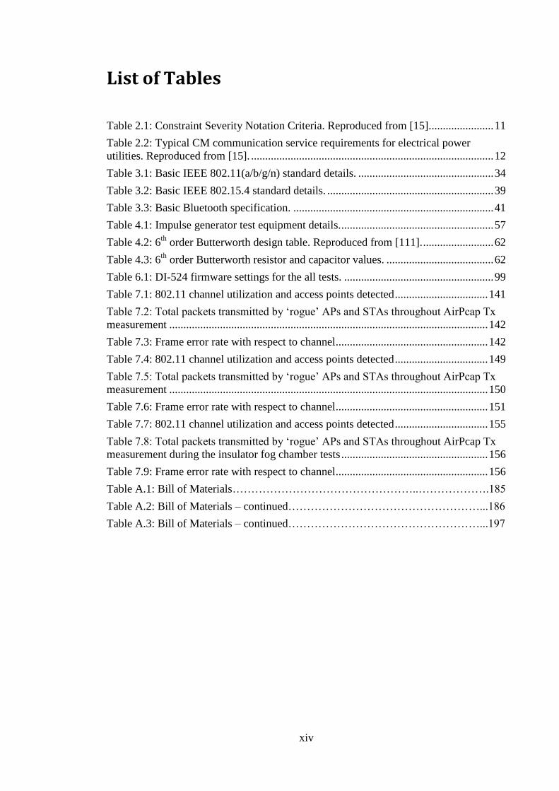
List of Acronyms
AES Advanced Encryption Standard
AC Alternating Current
ADC Analog to Digital Converter
CM Condition Monitoring
DAQ Data Acquisition
DC Direct Current
EPR Earth Potential Rise
EMI Electro Magnetic Interference
EDGE Enhanced Data rates for GSM Evolution
ESDD Equivalent Salt Deposit Density
ETSI European Telecommunications Standards Institute
FOP Fall Of Potential
FFT Fast Fourier Transform
FER Frame Error Rate
GDS Gas Discharge Tube
GIS Gas Insulated Substations
GPRS General Packet Radio Service
GPS Global Positioning System
GSM Global System for Mobile Communications
HV High Voltage
IMS Impedance Measurement System
ISM Industrial, Scientific and Medical
IEEE Institute of Electrical and Electronic Engineers
IC Integrated Circuit
IED Intelligent Electronic Device
IEC International Electrotechnical Commission
IP Internet Protocol
ISR Interrupt Service Routine
LED Light Emmiting Diode
LAN Local Area Network
MPPT Maximum Power Point Tracking
MOSFET Metal Oxide Field Effect Transistor
MOV Metal Oxide Varistor
MTS Mixed Technologies Switchgear
NSDD Non-Soluble Deposit Density
PD Partial Discharge
PCI Peripheral Component Interconnect
PIC Peripheral Interface Controller

xvi
PC Personal Computer
PCB Printed Circuit Board
P&C Protection & Control
PWM Pulse Width Modulation
RAM Random Access Memory
RSSI Received Signal Strength Indicator
R&D Research & Development
RMS Root Mean Square
SPI Serial Peripheral Interface
SSID Service Set Identifier
SMS Short Message Service
STA Station
SCADA Supervisory Control And Data Acquisition
TETRA Terrestrial Trunked Radio
THD Total Harmonic Distortion
TVS Transient Voltage Suppressor
TCP Transmission Control Protocol
UART Universal Asynchronous Receiver Transmitter
USB Universal Serial Bus
VI Virtual Instrument
VoIP Voice over Internet Protocol
WAP Wireless Access Point
WLAN Wireless Local Area Network
WIMAX Worldwide Interoperability for Microwave Access

1
Chapter 1 Introduction
1.1 Introduction
Since the manufacture of the first wireless telegraph in 1895, the radio waves are
bursting with the transmission of voice, data and other radio signals. FM and AM radio,
television, cellular phones, computers and many other devices make use of this means
of communications. Wireless technology has greatly improved since the wireless
transmission of Morse code, with an explosion of data transmission rates and a
reduction of cost and size of the radio.
The integration of a radio transceiver with a processing microchip, analog-to-
digital converter and other components has given rise to the wireless sensors. These
devices can be used to monitor the condition of equipment and sometimes also control
industrial processes.
Many industries have been quick to embrace this technological advancement,
while others have been more cautious. Though wireless sensors have many benefits
over wired ones, they also have their own set of problems. This thesis is intended to
shine light on both the potential benefits and obstacles in designing, testing and
applying wireless sensors in electrical substation environments.
Over the past 125 years, the electric power industry has grown to provide
electrical energy to billions of people worldwide. Wireless data communications is not
something new to the electric power industry, which has long been using it for power
system operations. Wireless technologies used include cellular radio systems, Private
Mobile Radio (PMR) networks, Terrestrial Trunked Radio (TETRA), paging systems,
licensed digital microwave and data telemetry via satellite (VSAT). These wireless
systems, which are often developed by manufacturers specifically for industrial
applications, have generally been used outside the substation or between the substation
and other sites, often for Supervisory Control And Data Acquisition (SCADA)
functions.
Copper point-to-point wires are traditionally used for substation communication,
usually between equipment in the substation yard and control equipment in the control

2
house. While substations are principally designed for the power equipment within them,
the communication infrastructure is essential to their reliable operation and physical
security. The safe and economic operation of any substation is linked with the use of
monitoring systems, which take advantage of the substation communication
infrastructure. Substation monitoring systems perform reliable acquisition, analysis and
storage of data, which are used to build ageing trends of the monitored assets, while also
attempting to predict their failure.
Permanently installed condition monitoring systems are known as on-line
Condition Monitoring (CM) systems. On-line CM systems are able to acquire larger
data sets and build trends of the health of the high voltage equipment they are
monitoring. The physical condition trends indentified by the on-line CM systems can
help facilitate predictive maintenance of substation equipment, which can be less
frequent and cheaper over the whole life of the equipment, compared to a utility‟s
traditional time based maintenance schedule.
Providing analysis and decision support, from the acquired CM data, in order to
indentify correctly equipment that require maintenance, is done using algorithms
running on dedicated computers. The algorithm‟s complexity, effectiveness of detecting
equipment failure and ability to translate raw CM data into a meaningful representation
of equipment condition, is an area where ongoing research is taking place [1, 2].
Typical substation CM systems are applied to a single piece of equipment, with
widespread deployment considered infeasible. However, widespread use of wireless
CM sensors within substations can take place without the laying of a single
communication cable. These wireless CM sensors can be battery powered, or take
advantage of mains supply where available [1].
This thesis explores the issues relating to a developed wireless CM system that
acquires continuous CM data from a wireless sensor, for short periods of time.
Traditional algorithms are then applied to the raw CM data, to transform them to a more
meaningful representation of equipment condition. Issues relating to the wireless
performance of the wireless CM system are also explored, as well as the solar powered
operation of the developed wireless CM sensor.

3
1.2 Justification for research
Ageing substation equipment is expected to operate at optimum efficiency
despite the fact that it might be reaching or exceeding its estimated operational lifetime.
Failure of aged substation equipment will inevitably lead to unplanned outages and
increased capital expenditure for the replacement of damaged assets.
On-line condition monitoring can help avoid unplanned outages by allowing
replacement of dangerously degraded assets, while effectively increasing the
operational lifetime of aged but healthy assets. The importance of on-line predicative
maintenance, improved sensing and developing expert systems for substations, was
recognized as long ago as 1991 [3].
It is unclear what percentage of substation equipment is retrofitted with
condition monitoring systems. A 2011 survey [4] identifies substation equipment
retrofitted with CM systems as below 20%. Utilities wanting to take advantage of CM
systems will have to bear the large cost for the cables and cable laying of wired CM
systems, while also planning a substation outage. Some or all of these costs can be
avoided with the use of wireless CM systems, which are a cost effective method for
existing and new substations. An added benefit of wireless CM systems is the
availability of a redundant communication channel to the wired substation SCADA
system.
There are a number of concerns about the use of wireless technology in a
substation environment. These concerns include the vulnerabilities related to the impact
of the noisy electrical environments on the wireless channel, the reliability of the
commercial wireless equipment, the consequences of overloading the unlicensed
frequencies due to many users, the performance for time-sensitive data, and the security
of communications.
The best method to understand the effectiveness and wireless performance of a
wireless CM system is through a realistic field testing in the exact location where the
system is to be deployed. The performance of a wireless CM system can be influenced
by the EMI in the substation, line-of-sight obstructions, large steel objects used in
substation equipment and overcrowded bandwidth. The performance of a wireless CM
system installed in a substation may change over time as additional substation plant is
installed altering the wireless transmission paths, as wireless CM sensors are installed,
or as increased numbers of users access the same unlicensed frequencies. Therefore, test

4
methodologies for determining the wireless environment in substations are necessary, if
wireless CM systems are to be used in substation environments.
A wireless CM system would consist of a number of wireless CM sensors
installed on equipment around the substation. CM data from the wireless sensors would
be transmitted to a central location, which could be the substation control house, to be
further passed on to the utilities‟ control or service center. Equipment diagnosis and
prognosis can take place within the wireless CM sensor, at a central database in the
substation control house or at the utilities control center.
From a utilities point of view, deciding on the required specification of a
wireless CM system is a very complex issue. Wireless CM systems can differ in
complexity and cost. Key differences may include: sampling rate, processing speed,
wireless data rate, onboard storage. Additionally the CM sensor may be battery powered
or AC mains powered. Furthermore, data processing can be a very power and time
intensive process. It can be very beneficial to acquire and process data in the wireless
CM sensor, rather than have to transmit the raw data to a centralized location. However,
if raw data is collected at a centralized location, more complex processing is possible,
and data from sensors monitoring different substation assets may be compared or used
together. The selection of a particular wireless CM system installed on a particular
substation asset, which adds the most value for a utility, is a complex one.
In this work, an investigation of on-line substation condition monitoring with an
interest in wireless CM sensors was undertaken. Wireless CM sensors using different
communication technologies were surveyed. A novel solar battery powered wireless
CM sensor was designed, manufactured, programmed and tested. Pollution monitoring
of high voltage insulators and the monitoring of earth impedance was examined.
Voltage and current measurements of two high voltage insulators in Cardiff
University‟s HV laboratory were carried out using the sensor, and the results were later
processed. The results were compared with those recorded directly through a data
acquisition card (DAQ) and transmitted via coaxial cable. Impedance measurements of
a 275kV earth tower base at the outdoor Llanrumney test field were carried out using
the sensor and the results were later processed. The wireless performance of the wireless
sensor was measured and compared for the laboratory and the outdoor environments.
The solar battery power operation of the wireless sensor was demonstrated in Cardiff
University‟s solar laboratory.

5
1.3 Contribution of research work
The novel aspects of the research can be summarised as follows:
The design, building and testing of a new wireless WLAN system was carried
out with careful selection of components and innovative approach to power
supply solution.
Comparative tests using the developed WLAN Sensor in a high voltage
environment to test polluted porcelain insulators took place measuring the
insulators operating voltage and leakage current.
Comparative tests with the WLAN sensor took place to measure the earth
impedance of a power transmission tower base measuring earth potential rise
and injected current.
A test methodology was developed and performed to determine the interference
characteristics of the WLAN and its performance under high voltage laboratory
and outdoor environments.
A developed wireless sensor that could be used for a wide variety of
measurements due to its bandwidth, and wireless connectivity.
1.4 Thesis overview
This thesis comprises 8 chapters including the introductory chapter and three
appendices. Chapter 2 covers on-line condition monitoring systems, including a review
of high voltage pollution monitoring of insulators as well as earth impedance
monitoring. Chapter 3 reviews the broad range of wireless CM sensor in electrical
substation environments presented in the literature, which use different communication
standards to exchange data with each other.
Chapter 4 describes the hardware components that make up the wireless sensor.
The results from the demonstration in a solar laboratory, of the solar battery powered

6
operation of the wireless sensor, are also presented in this chapter. Chapter 5 discusses
the operation of the wireless sensor, along with its firmware, which was written in the C
programming language. The LabVIEW software code used to control the operation of
the wireless sensor, save the wireless transmitted data and processed that data is also
presented in Chapter 5.
Chapter 6 presents the experimental setup and results for the polluted high
voltage insulator laboratory experiments. The experimental setup and results for the 275
kV earth tower base impedance measurements is also presented in this chapter. Chapter
7 presents the wireless performance of the wireless sensor that was measured and
compared, for a laboratory and outdoor environments.
Conclusions on the work presented in this thesis are drawn and suggestions for
future work are presented in Chapter 8. The three appendices offer supplementary
information towards the works presented in this thesis.
Finally, it is worth recalling that the topic of wireless sensors has a plethora of
acronyms, and while all attempts have been made to keep the acronym use to a
minimum, a small number of them repeatedly appear in this thesis.
7
Chapter 2 Overview of on-line condition monitoring and its application to outdoor insulators and earthing systems
2.1 Introduction
In this chapter an overview of on-line condition monitoring in electrical
substation environments was performed. The benefits that wireless sensors could bring
to CM in substations were investigated. The chapter then goes on to present some of the
current techniques and systems for pollution monitoring of high voltage outdoor
insulators as well as earth impedance monitoring. The information on condition
monitoring techniques and systems presented in this chapter is then used as a foundation
for the requirements needed for the development of a wireless CM system.
2.2 Substations
Substations perform a critical function in the electrical power industry by
transforming the voltage from high to low, or the reverse, or perform any of several
other control and switching functions. Electrical power may flow through several
substations between power plants and consumers, and its voltage may change in several
steps. A number of different equipment can be found in substations, generally divided
into switching, control & protection equipment and transformers. The substations
themselves are divided into two main categories of transmission and distribution
substations types. A transmission substation connects two or more transmission lines,
while a distribution substation transfers power from the transmission system to the
distribution system of an area, or is used to distribute power to local users.
The main considerations when designing a substation are cost and reliability.
Traditionally air-insulated substations, as seen in Figure 2.1, are the norm. However

8
where land is costly, such as in urban areas, Gas Insulated Substations (GIS) may be
more practical.
Figure 2.1: An example of an air insulated substation. Reproduced from [5].
Early electrical substations would be manned and all switching, equipment
adjustment and manual collection of any kind of data was performed manually. As the
complexity of the electrical power system grew, it became necessary to automate
supervision and control of substations from a central location. A number of technologies
have been used over the years for Supervisory Control and Data Acquisition (SCADA)
of substations, including dedicated copper wires, power-line carrier, microwave radio
and fiber optic cables.
Today, multiple intelligent electronic devices (IEDs) are used to communicate
with each other and supervisory control centers, using standardized communication
protocols such as DNP3, IEC 61850, and Modbus, to name but a few.
2.3 On-line condition monitoring in electrical substation environments
Power plant owners, transmission system owners and distribution system owners
have always been under pressure to improve their financial performance. More so today
in western developed countries, where a large number of equipment items are nearing

9
their end of life. In this environment, unexploited financial gains can be had from
improving the availability and lifespan of existing equipment, while reducing their
recurring maintenance and repair cost. Condition monitoring in electrical substation
environments has been reviewed in [4, 6-12]. The information gathered from condition
monitoring devices allows better engineering and financial decisions to be made. It
allows maintenance to be based on the condition of the equipment, and expensive asset
replacement work may be better prioritized [4, 6, 7].
Forward looking electrical power utilities realize that the above goals can be
achieved with improved maintenance planning, through the use of more and better
monitoring equipment [4, 6-8, 10]. In order for organizations to achieve the above
change in their business operation, on-line condition monitoring can be adopted.
The definition of on-line condition monitoring is probably best described as:
“On-line condition monitoring is the process of continuous measurements using devices
permanently installed on primary or secondary equipment, to collect and evaluate one
or more characteristic parameters with the intention of automatically determining and
reporting the status of the monitored subject at a certain moment in time” [4].
The four key components of a CM system are the sensor, data acquisition,
communication network and diagnosis [1, 13]. A sensor is a device that converts one
form of energy to another. Typically, a physical quantity will be converted to an
electrical value, which is then fed to the data acquisition (DAQ) component. The DAQ
comprises the analog to digital converter and possibly signal conditioning and signal
processing electronic circuits. The communication network will transmit the acquired
data locally to the control point in the substation, or to a central database. Finally, a
diagnosis will take place using CM data from one or more CM sensors. If an asset‟s
condition is detected to be at risk of failure, maintenance or asset management engineers
should be automatically informed.
An alternative architecture to a CM system has the diagnosis take place before
the transmission of the data. This CM architecture reduces the strain on the substation
communication network by decreasing the amount transmitted data. However, this
architecture might suffer from limited CM ability, due to the use of a simplistic data
processing algorithm, or due to the low number of physical parameters used detect
assets at risk of failure.

10
On-line condition monitoring can help utilities improve their asset management
processes. Asset management is a broad topic with a very large variety of subjects.
Four asset management themes can be influenced by a substation CM. These are
maintenance management, upgrading and capital investment management, utility risk
management and environmentally friendly service management [4].
A number of maintenance strategies exist, with the most basic being Time Based
Maintenance (TBM). Others include Reliability Centered Maintenance (RCM),
Condition Based Maintenance (CBM), Risk Based Maintenance (RBM) and
Performance Focused Maintenance (PFM). Detailed definitions of these maintenance
strategies can be found in [14]. Utilities must also optimize their planning of system
upgrading with the main challenge being to achieve higher service levels while
managing risks and avoiding unnecessary and ineffective investments. This can be
accomplished by improved asset condition and performance information of utilities
equipment, with the use of suitable CM systems.
Furthermore, CM can contribute to the minimization of a number of utilities
risks that are affected by the asset performance and can consequently increase the
network availability. For example, many utilities carry out maintenance works because
people responsible for switching equipment are used to time based maintenance and/or
they strictly obey manufacturer‟s instructions. However after dismantling of arc
extinguishing chambers of a circuit breaker to check the state of contacts and taking
apart operating mechanisms and putting them together again the general condition and
performance of the circuit breaker is not better and very often can be worse [6].
Environmental pressures and legislation have put demands on utilities to
reduce the unfriendly substances released into the environment and report about their
annual results. CM systems can measure the influence of the equipment service on the
environment [4]. How much value is added by CM systems to the asset management
process will vary with each utility.
2.4 Condition monitoring communication service requirements for electrical substations
Condition monitoring in the substation generates a large volume of time-critical
data to be transferred continuously to one or multiple platforms, hence creating the
necessity for a “monitoring network” across the substation telecommunication
11
infrastructure [15]. The associated architecture is utility-dependent, but a networked
environment around Ethernet, based on the IEC61850 standard, might become the main
interfacing technology for all data exchange applications in the electrical substation
[15]. Ongoing work is taking place by the IEC technical committee 57 working group
10, which is preparing a new IEC61850 part on condition monitoring, diagnostic and
analysis (IEC61850-90-3) [16].
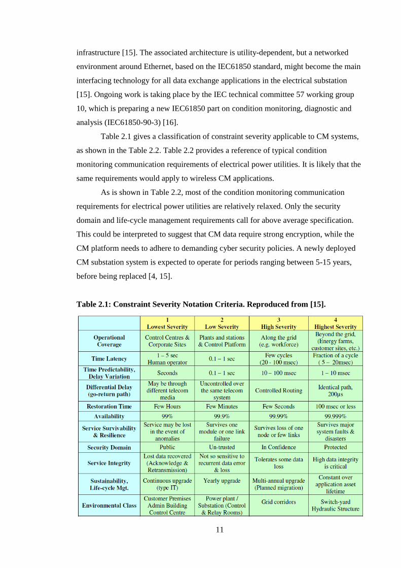
Table 2.1 gives a classification of constraint severity applicable to CM systems,
as shown in the Table 2.2. Table 2.2 provides a reference of typical condition
monitoring communication requirements of electrical power utilities. It is likely that the
same requirements would apply to wireless CM applications.
As is shown in Table 2.2, most of the condition monitoring communication
requirements for electrical power utilities are relatively relaxed. Only the security
domain and life-cycle management requirements call for above average specification.
This could be interpreted to suggest that CM data require strong encryption, while the
CM platform needs to adhere to demanding cyber security policies. A newly deployed
CM substation system is expected to operate for periods ranging between 5-15 years,
before being replaced [4, 15].
Table 2.1: Constraint Severity Notation Criteria. Reproduced from [15].
12
Table 2.2: Typical CM communication service requirements for electrical power
utilities. Reproduced from [15].
Requirements Rating
Coverage 2
Time latency 1
Delay variation 1
Differential Delay 1
Restoration time 1
Availability 1
Survivability 1
Security domain 3
Service integrity 1-2
Life-cycle Mgt. 3-4
Environment class 2
2.5 Applicability of wireless sensor networks in on-line condition monitoring of electrical substations
Wireless sensor technologies can play an important role in the industry‟s
evolution from traditional time based maintenance to condition based maintenance. The
increased demand for condition monitoring of plant equipment has incentivized
manufacturers of monitoring sensors to produce increasingly more capable sensors. This
refinement process of condition monitoring sensors inevitably gave birth to a sensor
fused with a wireless networking device. The wireless sensors underwent further
transformation, and widespread adoption was seen, for particular wireless sensors,
which operate using key wireless networking standards. The manufacturers and authors
of wireless networking standards and the users of wireless networking devices have
worked together over the years to address issues like security, data rate and coverage.
This process has produced more mature wireless networking standards, which in turn
led to wireless networking devices which can be used in broader applications.
The widespread adoption of wireless networking devices, such as 802.11 for
wireless internet connections throughout the facilities of organizations, has helped
spread the use of 802.11 wireless condition monitoring sensors, which use the same

13
802.11 wireless networking infrastructure. Wider availability of skilled personnel
throughout these organizations has helped support these wireless networks and the
technology is no longer perceived as niche. The widespread adoption of wireless
networking standards by manufacturers has also lowered the cost of wireless
networking devices, and users can purchase wireless devices and sensors from a large
number of manufacturers, which are compatible with each other.
Wireless sensor systems can play a role in substation condition monitoring, but
this role must take into account the realities of wireless vulnerabilities to electro-
magnetic interference, path obstacles, congestion of the limited frequency spectrum, and
other electrical factors [17].
CM applications where data would be very expensive to acquire using
traditional wired communications could benefit from the use of wireless sensors. In this
case, wireless sensors would shield against ground potential rises and reduce the
difficulty and cost of installing wiring across substation yards.
CM applications where the data transmitted is time sensitive and cannot tolerate
any delays, cannot use wireless sensors. Only CM applications that can operate when
data is lost for a length of time should use wireless sensors. This particular case of CM
monitoring applications can be subdivided into two distinct types: The first type of CM
application can wait while the data is buffered, if the wireless communication channel
becomes unavailable, the second can cope with loss of data due to wireless transmission
or reception difficulties. For example, cellular networks cannot be relied upon during
general emergencies, since it is very likely that their channels will be congested.
A wireless communication channel or a wireless sensor can be used for
redundancy purposes in condition monitoring applications. In this CM scenario, the
wireless communication channel is installed for redundancy purposes, which would
reduce the risk if the traditional wired data channel fails. The same goes for the wireless
sensor which provides redundancy to a wired sensor. As with a previous point made,
both of these CM redundancy applications need to tolerate potential losses or delays in
data transmission or reception.
While by definition on-line condition monitoring applications require the
permanent installation of sensors, a situation could arise where CM of equipment is
needed for a few hours, days or weeks. This could be because of a utility‟s drive for
surveying particular equipment, CM of older equipment that has no permanent CM
equipment installed, or possibly as part of strong indication of imminent equipment
14
failure [4]. Temporary CM might allow the risks to be better understood as a particular
type of plant defect is investigated.The speed and reduced cost of wireless sensor
installation in these cases would greatly benefit a utility, and any other disadvantages
are outweighed due to the temporary nature of the solution.
The ease of extending of a wireless network from within a power plant to its
associated substation is an advantage that utilities could benefit from. It is also very
likely that a combination of the scenarios presented above could persuade a utility to
install wireless sensor in their substations.
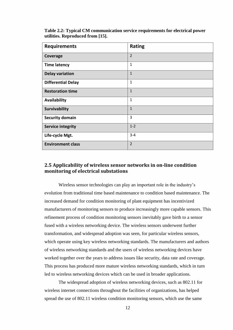
A 2007 survey of 83 utilities across 32 countries [18] shows that two utilities use
802.11 networks inside their substations to access IEDs, while 11 others planned to do
so. Another 14 utilities planned to install 802.11 networks that do not enter the
substation fence, while 30 others could see the benefits of this, but did not plan to do so.
Figure 2.2: Survey results on benefits of using 802.11 networks to access IEDs in
substations. Reproduced from [18].
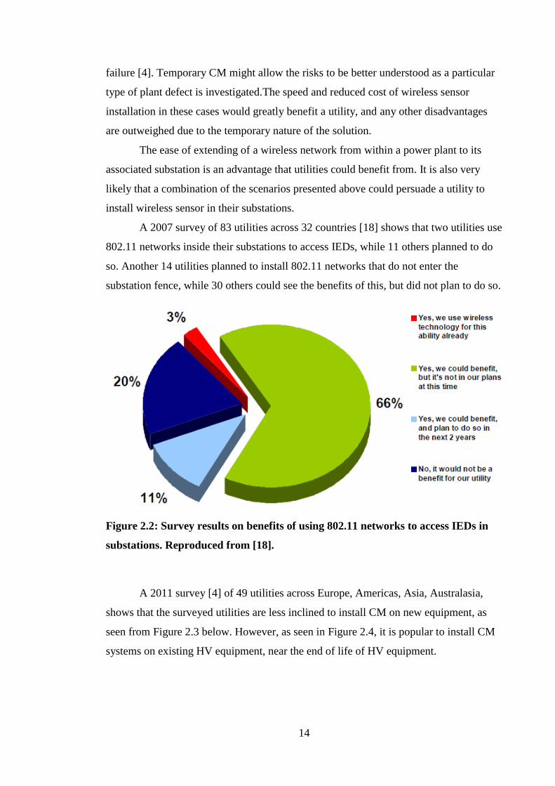
A 2011 survey [4] of 49 utilities across Europe, Americas, Asia, Australasia,
shows that the surveyed utilities are less inclined to install CM on new equipment, as
seen from Figure 2.3 below. However, as seen in Figure 2.4, it is popular to install CM
systems on existing HV equipment, near the end of life of HV equipment.
15
Figure 2.3: Results of survey on application of CM to new equipment. Reproduced
from [4].

16
Figure 2.4: Results of survey on application of CM to existing equipment.
Reproduced from [4].

17
Having to lay communication cables and possibly power cables many years after
the HV equipment was installed might involve a considerable cost to the utility.
Installing a wireless, instead of a wired condition monitoring sensor, could significantly
reduce the installation cost while also allowing for other equipment within the coverage
area of the wireless network to be monitored, which might have otherwise been cost
prohibitive. For example when the measurement of interest is in the coal yard, ash
disposal area, or transformer yard, the cost of cabling can be the highest cost of a project
[19]. Wire runs can be very expensive, with some cabling costing up to $2,000 per foot
(£4,134 per meter) [20].
Arguably the most appropriate method that would help utilities choose a
particular type of CM device is one that identifies which particular CM device best adds
financial value to a utility. However, the economic justification of substation CM
systems is also a complex issue, with differing approaches towards valuing and
justifying CM investments, depending on the types of assets in question [4, 6-8].
2.6 Substation assets
2.6.1 Introduction
As seen in Figure 2.3 and Figure 2.4 above, the most common application of
condition monitoring within substations reported by surveyed utilities is to
transformers. Second to transformers, switchgear, GIS equipment, surge arresters,
bushing and auxiliary equipment, see around the same level of CM equipment installed
on them.
Given that transformers and switchgear represent the largest capital expenditure
within a substation, it is not unusual for them to be two of the most common CM
applications. While a small population of complex components with high maintenance
and investment costs, like transformers, are attractive for condition monitoring, a larger
population of more simple components [10] is equally suitable for CM applications.

18
2.6.2 Insulator pollution monitoring
2.6.2.1 Factor affecting insulator performance
The reliability of power delivery systems is greatly dependent on the
performance of high voltage insulators. Outdoor insulator performance is reduced by
air-borne pollutant deposits which, when wet, reduce the insulator‟s electrical
properties.
Insulator pollution monitoring has been reviewed in [9, 21, 22]. Its main are
purposes are pollution site severity measurement, insulator characterisation and as an
initiator for insulator maintenance. A wide range of insulator pollution monitoring
techniques and devices have been developed over the years. The most widely used
techniques are directional dust deposit gauge, Equivalent Salt Deposit Density (ESDD),
Non-Soluble Deposit Density (NSDD), environmental monitoring (air sampling,
climate measurements), surface conductance, insulator flashover stress, surge counting
and leakage current measurement.
While all the above mentioned techniques and devices are being used in
substations, only a subset of them can measure the effects of both the pollution deposit
and natural wetting. Of those, two practical measurements are surge counting and
leakage current measurements.
2.6.2.2 Surge counting and leakage current measurements
The measurement of leakage current has been extensively used throughout the
world to assess glass and porcelain insulators for polluted conditions [22, 23]. The
leakage current across an insulator surface depends upon the service voltage and the
conductance of the surface layer. Also, the insulator flashover performance is estimated
from the leakage current measurement or the surface conductivity measurement.
While most of the present insulator leakage current instruments record the full
leakage current waveforms, this has not always been the case. It can be very beneficial
to only extract certain representative information from the leakage current waveform, as
recording the whole waveform can sometime be prohibitive, due to the very large data
files that would be generated. Surge counting and Imax measurement are two recognized
methods of extracting representative information from the leakage current waveform,
collected at the grounded end of the insulator.

19
In the surge counting method, only the number of leakage current pulses above a
fixed amplitude are recorded. Measurement data are collected from actual insulators
tested under service conditions. This can enable this simple monitoring method to
determine whether existing line or substation insulators need upgrading.
The Imax method, is the highest peak of leakage current that is recorded during a
given time period, on an insulator continuously energised at its service voltage. The
time period chosen is usually half a power cycle. This common method provides a
continuous record of the insulator performance under various weather conditions. By
doing so, this method provides information of all the stages of the flashover mechanism.
Data acquired using this method from insulators in outdoor environments can be
compared to one artificially polluted and tested in a laboratory. The need for line or
substation insulator upgrading can be determined using this method.
Through extended laboratory testing [23], it has been shown that a relationship
between the maximum current recorded during an artificial pollution test and the
pollution severity exists, if no flashovers occurred during the test. This relationship
differs for each type of insulator, but can be readily determined through laboratory
testing. A diagram illustrating such a relationship is shown in Figure 2.5. Using this
relationship both site severity and insulator performance can be determined.
Figure 2.5: A schematic impression of the relationship between leakage current
and the pollution severity as determined through laboratory testing. Reproduced
from [24].
As shown in Figure 2.6(a, b, c) the level of peak leakage current increases due to
salt deposition and the wetting of the insulator. Above a particular level of leakage
current, as represented by the vertical line in Figure 2.6(a), a flashover occurs. Leakage

20
current monitoring can thus be used as an early warning system to initiate maintenance
such as insulator cleaning, before a flashover occurs.
Figure 2.6: Schematic history of polluted ceramic insulators. Reproduced from
[23].
The pollution severity for a particular location can be determined using the
approach presented in the IEC 60815-1 standard [25]. According to the standard, on-site
leakage current measurements on a set of standard insulator types can be interpreted in
terms of the behaviour of the same type of insulators under artificial laboratory test
conditions.
The first step is to determine the relationship between leakage current and
pollution severity through laboratory tests on the insulator type of interest. The next step
is on-site monitoring of the leakage current across the insulator type for which the
leakage current relationship has been determined. The on-site monitoring of leakage
current has to continue for at least one year. Finally, the maximum current measured
during the whole monitoring period is converted to the equivalent pollution severity
using the relationship determined in the first step.
(b)
(a)
(c)

21
2.6.2.3 High voltage insulator monitoring systems
High voltage insulator condition monitoring systems have been developed by a
number of commercial entities and research institutions. A representative selection of
such systems is presented below. This section is not meant to be a detailed study of
these systems, rather it briefly explains the basic operation of such systems, identifies
the quantities they measure, the processing performed on those quantities, and finally
identifies the communication technology used to transmit the CM data to a centralized
location.
The Insulation Pollution Monitor (IPM), manufactured by TransiNor AS [26]
and seen in Figure 2.7 is designed to perform continuous on-line monitoring of external
pollution effects on high-voltage insulators and other insulator housings, like surge
arresters and bushings. The IPM can calculate the integral of the measured leakage
current, while also calculating the RMS value of the current. It measures the highest
peak of leakage current recorded during a given period of time. It can also measure the
number of leakage current pulses above given threshold levels, thereby generating a
statistical distribution of the leakage current. All data is stored in the data acquisition
unit and is available through a communication interface. The stored data can be
retrieved using an RS232 modem, an Ethernet network card, a memory stick, a standard
modem or a GSM modem. The data can be downloaded for further analysis with
dedicated software or spreadsheet application like Microsoft Excel. The system can be
set to issue alerts when certain threshold values are exceeded.
Figure 2.7: Simplified diagram of the IPM system. Reproduced from [26].
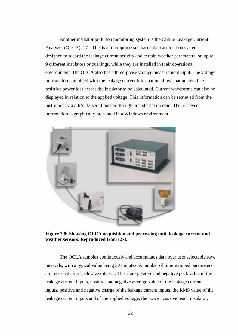
22
Another insulator pollution monitoring system is the Online Leakage Current
Analyzer (OLCA) [27]. This is a microprocessor-based data acquisition system
designed to record the leakage current activity and certain weather parameters, on up to
9 different insulators or bushings, while they are installed in their operational
environment. The OLCA also has a three-phase voltage measurement input. The voltage
information combined with the leakage current information allows parameters like
resistive power loss across the insulator to be calculated. Current waveforms can also be
displayed in relation to the applied voltage. This information can be retrieved from the
instrument via a RS232 serial port or through an external modem. The retrieved
information is graphically presented in a Windows environment.
Figure 2.8: Showing OLCA acquisition and processing unit, leakage current and
weather sensors. Reproduced from [27].
The OCLA samples continuously and accumulates data over user selectable save
intervals, with a typical value being 30 minutes. A number of time stamped parameters
are recorded after each save interval. These are positive and negative peak value of the
leakage current inputs, positive and negative average value of the leakage current
inputs, positive and negative charge of the leakage current inputs, the RMS value of the
leakage current inputs and of the applied voltage, the power loss over each insulator,

23
mean temperature, humidity, Ultraviolet B (UVB), wind speed, wind direction and
rainfall. Such a system was installed to monitor an in-service insulator performance test
tower, on a 220 kV electrical power line close to the Walmund substation in Namibia
[28].
While all the leakage current monitoring systems presented thus far are
relatively complicated systems that measure and save a number of different parameters,
a different approach is presented in [24]. The leakage current monitor, seen in Figure
2.9 was designed as a low-cost, robust device compatible with the requirements for
using radio backscatter technology. Applications of such a device are for power lines
and substations to monitor the insulator performance under polluted conditions. This
device only stores the statistical parameters of the leakage current peaks that occurred
during the monitoring period. No other leakage current parameters are recorded. The
developed sensor is a self-contained unit which connects to the insulator base and
communicates its recorded data wirelessly through backscatter technology to a data
interrogator over a distance of 50 m. This device also allows data collection from a
moving vehicle with a speed of up to 100 km/h. The sensors can also be used in an on-
line monitoring mode, where they are polled from a base station on a regular basis.
Figure 2.9: Backscatter leakage current monitor installation on a substation
insulator. Reproduced from [24].
Further high voltage insulator condition monitoring systems with characteristics similar
to the ones presented above can be found in [29-33].
HV Insulator
HV Insulators
Metal plate
allowing for the
leakage current
to flow into the
sensor.
Earthing
cable

24
2.6.3 Earth impedance testing
2.6.3.1 Introduction
Insulation leakage currents and minor three phase AC system imbalances will
always channel relatively small currents into the earthing system of a substation.
Substation fault conditions can generate power frequency fault currents from a few kA
up to 20-30 kA, and earth impedances of high voltage substations may lie in the range
from 0.05 Ω to over 1 Ω [34]. Several tens of kA of current in the substation earthing
system can also be generated due to lighting transients.
The potential of the substation earthing system will rise with respect to a remote
reference environment as the current flowing into it increases. Human beings and
livestock can be exposed to dangerous voltage levels if the substation earthing system
potential exceeds certain levels. Minimizing the risk of death or injury to staff, visitors,
pedestrians or trespassers in and around substations due to earth potential rises is an
important issue to utilities.
The tolerances of the human body to currents with frequencies of 15-100Hz is
level and time dependent [35]. Similarly, a correctly designed substation earthing
system will be one that minimizes the earth potential rise through a low earth
impedance value that is maintained throughout the operational life time of the
substation. Protection devices with adequate performance will also be required to
minimise the time of exposure to earth potential rises.
Maintenance and integrity testing intervals for a substation earthing system can
be as far apart as five or six years. Without the use of a continuous impedance
monitoring system for a substation earthing system, a failure between two test intervals
could go unnoticed. The undetected failure of part of a substation earthing system due to
corrosion, damage from high fault currents or theft of the equipment earthing joints can
pose a serious risk to the health and safety of individuals in or around a substation.
2.6.3.2 Fall-Of-Potential impedance measurement technique
While substation earth resistance measurements were used in the past to
characterize such systems, the reactive component of large area earthing systems may
be significant, making it essential to carry out earth impedance rather than resistance
testing [34].

25
An ideal representative test for the impedance measurement of a substation
earthing system is the staged fault test [36]. However, the economic penalties and
system operational constraints due to the need to disconnect the substation from the grid
to perform the test, means that this type of test is seldom performed.
The most common earth impedance measurement technique is a variation of the
Fall-Of-Potential (FOP) technique. For the earth impedance measurement, AC instead
of DC is circulated between the substation earthing system and the auxiliary current
electrode, as seen in Figure 2.10. In order to reduce the mutual coupling between the
current electrode and the voltage electrode, a 90° angled test arrangement is
recommended. This „90° method‟, as it is commonly known, reduces the mutual
coupling between the two test leads, but does not completely eliminate it [37]. The
voltage electrode can be assumed to be at remote zero potential, as long as the distance
between the current and voltage electrodes is 6.5 times the extent of the earthing system
[36].
Figure 2.10: Impedance measurement of an earthing system. Reproduced from
[36].
With the voltage electrode at remote zero potential, and assuming that the
measurements are not influenced by mutual coupling or other interference, the system
impedance may be found by Equation (1) below:
(1)
26
A number of types of current injection equipment can be used to perform the FOP
impedance measurement technique. Several signal detection techniques can be used
with each of the current injection equipment.
One of the simplest instrumentation methods to calculate earthing impedance
requires a 1:1 isolation transformer, a stable oscillator, a power amplifier, a differential
probe, a current transformer and an oscilloscope. Earth impedance measurements and
simulations using the 90° FOP method, have provided good results [38]. It should be
noted that while the impedance at power frequency is of interest, due to the interference
created by substation equipment, measurements at frequencies either side of 50 Hz need
to be performed instead. The impedance at 50 Hz can then be obtained by interpolation.
2.7 Summary
Condition monitoring of existing and new electrical substation equipment is of
increasing importance to utility companies. The physical condition trends built by the
on-line CM systems can help facilitate predictive maintenance of substation equipment,
which can be less frequent and cheaper over the whole life of the equipment, compared
to a utility‟s traditional time based maintenance schedule. Wireless CM sensors can be a
cheaper alternative to wired ones, thus allowing for a larger population of substation
equipment to be monitored. Wireless sensors can play a role in CM of electrical
substation environments, but this role must take into account issues like data delay or
data loss due to interferences. CM of high voltage outdoor insulators can be used to
predict when a particular insulator needs cleaning. The failure of a a substation earthing
system can be detected through a continuous impedance monitoring system, which
might otherwise go undetected.

27
Chapter 3 Wireless sensor technologies in electrical substation environments
3.1 Wireless sensor design and components
3.1.1 Introduction
This chapter begins by presenting the basic components of a wireless sensor and
continues by explaining some of their key properties. The broad range of wireless CM
sensors in electrical substation environments presented in the literature, which use
different communication standards to exchange data with each other, are then reviewed.
The purpose of this review was to understand the specification, performance and
deployment of the many wireless CM sensors currently being piloted, or in use within
electrical substation environments.
3.1.2 Wireless sensor components
The human need for information exchange, whether that information is audio,
visual, text, or simple data, without the use of cables, produced a large number of
relatively cheap and successful wireless network technologies have a history of more
than 110 years. These wireless networks require two or more wireless transceivers that
communicate with each other. In order to facilitate a cost effective collection of data
from one or more locations to a central one, wireless sensors can be used. While a
personal computer will ultimately be used at the central location to store and possibly
further process the collected data, cheaper wireless sensors will be used to collect the
necessary data at the remote end. The principal components of a wireless sensor needed
to facilitate wireless communication are illustrated in Figure 3.1.

28
Figure 3.1: Basic components of a wireless sensor.
The microprocessor helps facilitate data capturing and data processing while, at
the same time, deciding when to pass or receive data from the wireless transceiver. The
microprocessor will have some on-board memory but the wireless sensor might have
more memory storage in the form of a memory microchip. The input/output interface
includes all the required components that pass information to the microprocessor from
the „real‟ world and relay information from the microprocessor to the „real‟ world. The
input interface can be any kind of transducer, such as a microphone, a pressure sensor, a
light detector or a current transformer. The input interface might include an analog-to-
digital converter (ADC). The output interface can be any kind of transducer e.g. a
screen, a light display, a motor, or a speaker. The output interface might include a
digital-to-analog converter (DAC).The wireless transceiver is generally one or more
microchips equipped with by an antenna, which facilitates the wireless communication
of information. The power supply can be any kind of power converter and/or battery.
The power supply can often include some form of energy harvesting like solar, wind,
inductive, capacitive or vibration system as the source of energy.
3.2 Key wireless sensor properties
3.2.1 Communication
The wireless transceiver is used to exchange data between wireless sensors. In
this chapter it is shown that most wireless networks that are used for communication in
power system environments, use frequencies from 868 MHz to 5 GHz. A number of
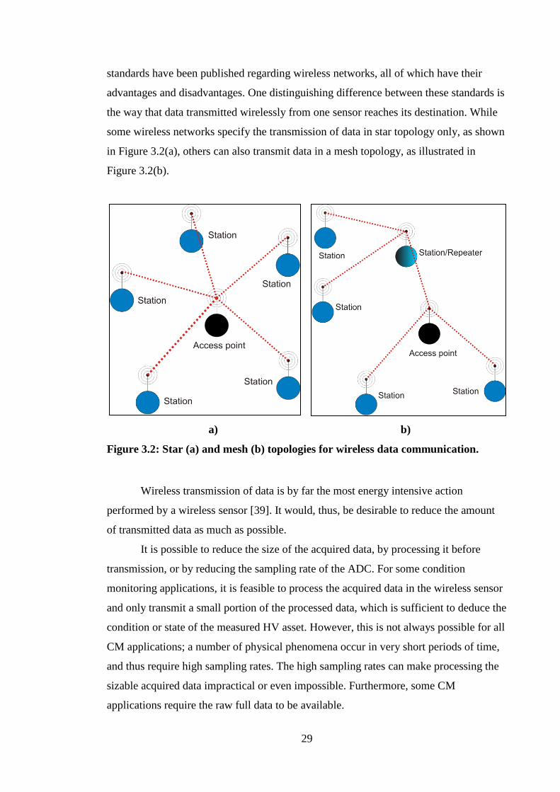
29
standards have been published regarding wireless networks, all of which have their
advantages and disadvantages. One distinguishing difference between these standards is
the way that data transmitted wirelessly from one sensor reaches its destination. While
some wireless networks specify the transmission of data in star topology only, as shown
in Figure 3.2(a), others can also transmit data in a mesh topology, as illustrated in
Figure 3.2(b).
a) b)
Figure 3.2: Star (a) and mesh (b) topologies for wireless data communication.
Wireless transmission of data is by far the most energy intensive action
performed by a wireless sensor [39]. It would, thus, be desirable to reduce the amount
of transmitted data as much as possible.
It is possible to reduce the size of the acquired data, by processing it before
transmission, or by reducing the sampling rate of the ADC. For some condition
monitoring applications, it is feasible to process the acquired data in the wireless sensor
and only transmit a small portion of the processed data, which is sufficient to deduce the
condition or state of the measured HV asset. However, this is not always possible for all
CM applications; a number of physical phenomena occur in very short periods of time,
and thus require high sampling rates. The high sampling rates can make processing the
sizable acquired data impractical or even impossible. Furthermore, some CM
applications require the raw full data to be available.

30
3.2.2 Synchronization
Time plays an important role in the operation of wireless sensors, since they are
monitoring time-varying physical phenomena. An accurate time reference is needed so
that a wireless sensor can timestamp acquired data accurately.
The time reference of a wireless sensor is dependent on the accuracy of
hardware clock it is using. The vast majority of wireless sensors use quartz crystal
oscillators as their clock. Oscillators have a random deviation from their nominal
frequency, called drift. The clock drift is expressed in parts per million (ppm) and gives
the number of additional or missing oscillations. The oscillator drift value quoted by the
manufacturer is also influenced by fluctuations of voltage, age and temperature. It was
reported from the field of wireless sensor networks that, clocks have been found to drift
in the range between ±1 and ±100 ppm [40, 41].
3.2.3 Sampling and processing
A great range of monitoring applications in electrical substation environments
could benefit from the use of wireless sensors. While differing sampling rates would be
required for each monitoring application, the wireless sensors need to operate within a
set of limited resources. A wireless sensor has a limited speed and memory, with the
possible constraints on the energy available to it as well. The correct selection and
combination of the basic components making up a wireless sensor will determine
whether it is considered successful for a particular CM application.
A very large number of microprocessors are commercially available, which can
be used for data sampling and processing. A complex relationship exists which
determines the choice of microprocessor and ADC. Microprocessors parameters like
cost, architecture, speed, internal memory size and power consumption play an
important role in the decision making. The choice of microprocessor will also be
heavily influenced by the projected amount of acquired data and speed required for data
processing. As mentioned earlier, the required amount of acquired data and processing
speed required will be heavily dependent on the CM application itself.

31
The ADC specification will also influence which microprocessor is chosen to
operate in the wireless sensor. It is common for microprocessors to contain their own
ADC, however, a more specialized ADC which is external to the microprocessor can be
used for more demanding monitoring applications.
3.2.4 Lifespan and Energy Harvesting
The availability energy to power the wireless sensor will also determine whether
a wireless sensor can be applied to a particular condition monitoring application. If
energy is readily available, either directly from mains supply, or from some other
unlimited energy harvesting power supply, then the wireless sensor has no urgent need
to limit energy consumption. However, when only a limited amount of energy is
available to the wireless sensor, relative to its energy consumption, further consideration
is needed so that its overall operation becomes more energy efficient.
A number of techniques are available reduce the energy consumption of the
wireless sensor while not sacrificing its ability to operate successfully for a particular
application. For example, performing the data acquisition function at periodic intervals
only is one option for reduced energy demand. Another option would be to process the
acquired data, thus transmitting a smaller volume of data. Furthermore, it is also
feasible to acquire and store data continuously and only begin wireless transmission of
data if a certain threshold value or event occurs. It is also possible to have the
microprocessor „wake up‟ from a low power mode, with the use of a „detect-and-
trigger‟ electronic circuit, which monitors an input and forces the microprocessor to
acquire data if an event of interest occurs [42]. The last technique will, however, require
that the event being monitored is slow enough for the microprocessor to wake up from
its low power mode.
Most microprocessors are well suited to this kind of operation, which reduces
their overall energy consumption [43-45]. A range of speed and energy consumption
options are available for most microprocessor. The lowest energy consumption
available, commonly referred to as „sleep mode‟, will force the microprocessor to run at
the lowest possible speed, only „waking up‟ periodically to acquire data or to perform
other operations. An intermediate energy consumption level for microprocessors,
referred to as „doze mode‟, will allow the microprocessor to process or acquire data at a

32
slower speed, while at the same time conserving energy compared to the its fully „active
mode‟. Figure 3.3 shows the variation of the power consumption with time, depending
on the operational need of the wireless sensor.
Figure 3.3: Simplified example of varying power consumption over time for a
wireless sensor.
While wireless sensors can be powered from a mains supply, it can be
advantageous to remove the need for power supply cabling if possible. Depending on
the power consumption of the wireless sensor, its power supply can be a purely battery
powered solution, with the batteries being replaced when necessary or every time
maintenance is taking place at a substation. However, replacing the batteries at a regular
interval might not always be possible, due to the associated high labour cost. With
wireless sensors that have an event driven operation and do not accurately measure or
estimate their own battery‟s capacity, it can be difficult to estimate [46] the replacement
period required. The solution to this problem could be the introduction of a renewable
power supply source. This power source could be used without the need for a battery, if
it is able to supply the energy needs of the wireless sensor at all times. A „hybrid‟
approach that uses a renewable power supply source which charges a battery is usually
more practical [47].
A number of renewable and other electromagnetic sources like wind, solar,
vibration, inductive and capacitive could be used in power system environments.
However, wind and solar are more likely to be used in outdoor substations and are
highly dependent on the local climate conditions. If the exact power needs of the

33
wireless sensor are known, local historical data for wind speed and solar irradiance can
be used to determine the required power rating of the renewable source. According to
[48], solar battery powered wireless sensors are being investigated for use in an outdoor
substation environment. Inductive and capacitive energy harvesting from the
electromagnetic fields produced by substation power lines and busbars is being
investigated [1, 49-52]. While these two types of energy harvesting methods can be
used at indoor and outdoor substations, they are limited to air insulated ones. Vibration
harvesting in electrical substation might be possible by mounting the scavenging device
to the damper at the base of a power transformer [1, 50].
It should be noted that while a rechargeable battery can discharge its energy over
the temperature range of -20 to 60°C, when being charged, its temperature range has to
be within 0 to 45°C [53, 54]. The battery charging microchip will interrupt the charging
cycle, if this temperature range is exceeded. This fact can limit the application of a
hybrid power source to locations that have mild climatic conditions throughout the year.
However, it is feasible to design a wireless sensor that maintains its battery temperature
to within the required temperature limits.
3.3 Wireless network standards
3.3.1 IEEE 802.11 a/b/g/n wireless networks
Second only to cellular networks, IEEE 802.11 wireless local area networks
(WLAN) are the most commercially successful wireless data networks. The 802.11
standard describes an over-the-air interface between a wireless client, referred to as a
station (STA) and a base station, referred to as a wireless access point (WAP). A large
number of 802.11x standard amendments have been published since 1997 and many
others are at various stages of being ratified. Published amendments include security
enhancements like 802.11i [55] while others under development, e.g. 802.11ac which
defines higher data throughput. The most commercially successful and widely used
standard amendments are shown in Table 3.1 below, with some of their respective
specifications.

34
Table 3.1: Basic IEEE 802.11(a/b/g/n) standard details.
IEEE standard amendment
Approval date
Operating frequency (GHz)
Maximum theoretical data rate (Mbps)
Maximum outdoor range (m)
802.11a 1999 5 54 120
802.11b 1999 2.4 11 140
802.11g 2003 2.4 54 140
802.11n 2009 2.4/5 600 250
The 802.11(a/b/g/n) [56, 57] devices all use the Industrial, Scientific and
Medical (ISM) license free frequency bands. The ISM radio portions used by 802.11
devices change slightly from country to country, but the European Telecommunications
Standards Institute (ETSI) defines them at 2.4-2.5 GHz and 5.47-5.725 GHz. As the
name of the band implies, these frequencies were intended for uses other than
communication, like radio-frequency process heating and microwave ovens. However, a
large group of the devices using these frequencies are in fact short range, low power
communication systems, like 802.11 wireless networks. The use of microwave ovens,
non-802.11 cordless phones and any other non-802.11 device, can be a large source of
interference for 802.11 devices when operation of the same frequency [58, 59]. A
number of options are available to 802.11 network users to mitigate this interference,
like forcing an 802.11 network to change frequency channel. Figure 3.4 below shows
the 802.11 channels available in the 2.4GHz band. While different 802.11 networks
operating on the same channel have mechanisms designed to share the ISM frequency
spectrum between them, the channel sharing is contentious [60-63]. While any of 13
channels are available for use in Europe, it is most common for channel 1, 6, or 11 to be
used. One reason for this is frequency overlapping between adjacent 802.11 channels
causes a reduction in data rate [64].

35
Figure 3.4: Graphical representation of 802.11 channels in 2.4 GHz band.
Reproduced from [65].
Since the publication of the 802.11 standard in 1999, it has become clear that the
original data confidentiality mechanism defined by the standard had numerous flaws
[66, 67]. The 802.11i amendment was developed and ratified in 2004, in which the
secure Advanced Encryption Standard (AES) is used to overcome the security
weaknesses of the original standard. The National Security Agency (NSA) has stated
that the AES specification is secure enough for classified as well as un-classified U.S.
government data. The 802.11w [68] amendment was ratified in 2009 to protect against
network disruption caused by malicious systems, however, according to [69], this will
offer only partial protection.
Due to the known past and present 802.11 vulnerabilities, availability, secure
access and confidentiality are the three primary concerns of utilities who may wish to
use. It is unclear to what extent802.11 networks are susceptible to substation
electromagnetic interference and how this might affect the availability of a 802.11
wireless network. Issues such as overloaded bandwidth, disruption of the wireless data
rate due to electromagnetic interference (EMI) and weak signal strength due to large
distances, have to be examined for each monitoring location, as they might vary greatly.
Frequency (MHz)

36
If a wireless CM sensor is mounted on high voltage conductors, it is unknown to what
extent interference from high frequency signals such as corona will affect the
performance of the wireless sensors. For example, some published results [70] showed a
clear correlation between vacuum and SF6 gap breakdown and a sharp decline in the
data rate of two 802.11b devices. Secure access and confidentiality can be resolved with
the use of the 802.11i standard that provides robust security, both in terms of data
encryption and network connectivity.
The Electric Power Research Institute (EPRI), in Palo Alto, US and the Pacific
Northwest National Laboratory, in Richland, US along with their partner utilities have
both piloted a significant number of projects in condition monitoring of power plant
equipment using wireless sensors. While the focus of these publications is on wireless
sensors for power plant equipment, it would be wrong to ignore these relating and
detailed publications. The close physical, business and operational relation between
power plants and substations, make any knowledge learned in wireless condition
monitoring in one field, relevant to the other. For example both the 802.11 wireless CM
sensors and access points, operating in a power plant, could be extended to its related
substation.
The Baldwin Energy Complex Coal Plant in Baldwin, United States, installed 8
vibration sensors on its coal pulverizer along with a data acquisition board and used an
802.11b network to transmit the data via the plant‟s local area network to a dedicated
desktop computer for analysis [71]. More information on the benefits of the wireless
data acquisition system is not publically available.
The San Onofre Nuclear Generation Station at San Clemente, United States, had
been experiencing failures of its circulating water pump motors due to clogging of
internal cooling passages which reduced air flow within the passages. Existing
thermocouples in their water circulating pumps/motors were used to measure their
temperature and transmit it wirelessly using an 802.11b network to the plants main
LAN network [19]. It should be noted that though the pumps/motors had existing
thermocouples installed in them, they were not previously used as part of a monitoring
system, with 13 motors having failed since the power plant start up. Since the wireless
installation was deployed in 2003, not a single motor has failed during plant operation
as enough forewarning is given by the monitoring system to replace failing pumps.
A proof-of-concept wireless vibration data acquisition system was tested at the
Comanche Peak nuclear power plant in the United States [72]. For the project, the plant

37
installed 94 wireless sensors on generation-critical equipment, including pumps, motors
and turbines in the Comanche Peak Unit 2 building. The sensors monitor vibration and
other parameters and transmit the data wirelessly to access points in the plant that are
linked to a fiber optic backbone. This backbone ties to the plant site‟s local area
network, enabling plant technicians to access the sensor data for predictive maintenance
analysis. The plant has over 400 access points (802.11b) installed, covering the whole
Comanche Peak power plant facility. The 802.11b network was initially installed for
use with VoIP phones (Voice over Internet Protocol) that are deployed at the station and
for piloting IP video surveillance monitoring. More information on the benefits of the
wireless sensors mentioned in the pilot study above are not publically available.
An 802.11g wireless data acquisition system was used at the High Flux Isotope
Reactor (HFIR), at the Oak Ridge National Laboratory, Oak Ridge, United States. The
wireless data acquisition system was used to measure the vibration of two sets of
motor/fans, which are part of the reactor building ventilation system. A wired data
acquisition system was used in conjunction with the wireless one and the results showed
good agreement between wired and wireless systems [73].
A number of other power plants have been reported to have installed 802.11
access points for their VoIP phones, 802.11 cameras and general data communication
needs. Arkansas Nuclear One, in Russellville, United States, installed 145 access points
(802.11) that provide site wide access to the wireless network for VoIP phones,
laptop/PDA communication and camera monitoring [74]. The Farley nuclear power
plant in Dothan, United States also has 802.11 access points that provide site wide
access to the wireless network for VoIP phones, laptop/PDA communication and
camera monitoring [74].
While no publications were found to discuss the application of 802.11 wireless
networks for substation protection and automation, the 2007 survey of 83 utilities across
32 countries [18] indicates that utilities are considering the technology for that use,
while at the same time using it for other operational applications, as illustrated in Figure
3.5 and Figure 3.6.

38
Figure 3.5: Use of 802.11 wireless networks for electric power systems applications.
Reproduced from [18].
Figure 3.6: Use of 802.11 wireless networks for general applications by electric
power utilities. Reproduced from [18].

39
3.3.2 IEEE 802.15.4 wireless networks
The primary goal of the IEEE 802.15.4 is to provide reliable, power efficient
communication capabilities for low data rate wireless networks. A number of protocols
have been developed to work with the 802.15.4 standard [75]. ZigBee, WirelessHART
and ISA100.11a are currently the most well known. A number of companies including
ABB [76], Siemens [77], Emerson [78] and Honeywell [79] offer wireless sensors
based on the 802.15.4 standard. Table 3.2 shows the basic information of the IEEE
802.15.4 standard. While 802.15.4 wireless sensors can use one of three different
frequency ranges, the most commonly used is the 2400-2483.5MHz. One of the major
benefits of 802.15.4 sensors is that they can form a mesh network, where each sensor
does not only transmit its own data, but also serve as a relay for other sensors, as was
shown in Figure 3.2(b). A number of security issues have been identified [80] with
regards to the 802.15.4 standard, but the 2006 and 2011 revisions of the IEEE 802.15.4
have addressed most these security flaws.
Table 3.2: Basic IEEE 802.15.4 standard details.
Frequency band (MHz)
Maximum theoretical data rate (kbps)
Maximum range (m)
868.0-868.6 100 75
902-928 250 75
2400-2483.5 250 75
A proof of concept 802.15.4 wireless sensor network was developed for
temperature monitoring in electrical substations [81]. A more advanced proof of
concept used a 802.15.4 wireless sensor which is designed to act as a base station and
locally store data from other wireless sensors while also measuring the 3-phase voltage
on the busings of a power transformer. The acquired 3-phase voltage data are then
processed and an estimate of their phase differences is found, so as to monitor the health
of the transformer bushing [82].
A detailed study using 122 wireless sensors (802.15.4) is presented in [48]. The
study took place at a high voltage substation in Paradise, Kentucky, United States,
where the ambient temperature as well as surface temperature of the circuit breakers and
transformer oil tanks were periodically measured. The vibration and sound of oil cooled

40
transformers was periodically measured as well as the SF6 gas density of circuit
breakers.
Partial discharge monitoring of power transformers using 802.15.4 wireless
sensors has also been suggested in [83]. A partial discharge monitoring wireless sensor
was programmed and tested in [1, 84-86], where it was found to be able to detect
multiple defects and capable of rudimentary defect classification in power transformers.
A wireless surge arrester leakage current sensor, based on the ZigBee protocol,
was developed and tested in a 230kV substation, by the Sao Francisco Hydroelectric
Company [87]. Three wireless sensors were installed on different surge arresters and the
acquired leakage current was transmitted over a distance of 400 meters to the substation
control room.
The San Onofre Nuclear Generation Station at San Clemente, United States, was
due to have its high pressure turbine replaced by 2011, and it was decided that the
performance of the old turbine was to be investigated. In November 2009, 10
WirelessHART (802.15.4 based) wireless pressure transmitters were installed to
monitor the HP inlet turbine pressure [74].
Mistras Group Inc. has developed a number of wireless sensors based on the
802.15.4 standard. A wireless SF6 circuit breaker gas leak detection sensor has been
developed and has been made commercially available [88]. This wireless sensor can be
supplied with a lithium battery, or with a solar powered rechargeable lead acid battery.
The company has also developed a wireless acoustic emissions sensor based on the
Zigbee standard [89]. No detailed information on the wireless sensor performance has
been published for the SF6 circuit breaker gas leak detection sensor or the acoustic
emissions wireless sensor. However, anecdotal evidence [90] suggests that six acoustic
emission wireless sensors were used to monitor partial discharge activity on six gas
insulated 765kV current transformers inside an electrical substation. At a different
electrical substation, seven acoustic emissions wireless sensor were used to measure PD
activity on seven oil circuit breakers while five wireless sensors were used to measure
PD activity on five Voltage Transformers (VT).

41
3.3.3 IEEE 802.15.1 (Bluetooth) wireless networks
Bluetooth is a proprietary open wireless technology standard for exchanging
data over short distances. Table 3.3 summarizes the basic Bluetooth specifications with
respect to the standards version. A network of Bluetooth devices, known as a piconet,
can contain one master and seven slave Bluetooth devices. The connection of two or
more piconets form a scatternet in which certain devices simultaneously play the master
role in one piconet and the slave role in another. The primary use of a Bluetooth device
is as a low power, wire-replacement device. A number of security flaws have been
identified for Bluetooth devices [91, 92]. Significant changes to Bluetooth's security
have been made that overcome previous security flaws. However, old devices remain
vulnerable.
Table 3.3: Basic Bluetooth specification.
Version Frequency band (GHz)
Maximum theoretical data rate (Mbps)
Maximum range (m)
Classic 2.4-2.4835 1-3 100
High speed 2.4-2.4835 24 100
Low energy 2.4-2.4835 1 50
While the popularity of Bluetooth devices is undisputed, their application in
power system environments has seen limited use. A wireless Electromagnetic
Interference (EMI) sensor using Bluetooth as the communication interface has been
developed [93, 94]. Testing of the wireless sensor against a fiber optic system, using a
portable electric and magnetic generator, showed good agreement between the two data
acquisition systems [95].
3.3.4 Second, third and fourth generation cellular networks
Cellular networks are the most commercially successful wireless data networks.
While a number of competing cellular networks were operating throughout the world,
eventually, the standard referred to as Global System for Mobile communications
(GSM) became the most popular. This standard often referred to as 2G, short for second
42
generation, initially only supported voice communication and not digital packet data
transmissions. However, it did eventually evolve to support data transmissions. The
General Packet Radio Service (GPRS) is a packet data communications built on top of
the GSM technology. GPRS offers maximum download and upload speeds of 60 kbps
and 40kbps respectively. A further enhancement on GSM was Enhanced Data rates for
GSM Evolution (EDGE), which improved the theoretical maximum possible download
and upload speed to 473.6 kbps and 315.7 kbps respectively. While encryption is
implemented in GSM, GPRS and EDGE, several weaknesses have been shown to exist
with it [96, 97].
Third generation (3G) cellular networks have brought much higher data rates,
but limited coverage is offered throughout most countries, generally limited to major
urban areas. The two main competing technologies are High-Speed Packet Access
(HSPA) and Evolution-Data Optimized (EV-DO). HSPA supports maximum possible
download and upload speeds of 14 Mbps and 5.76 Mbps, respectively. EV-DO supports
maximum possible download and upload speeds of 14.7 Mbps and 4.9 Mbps,
respectively.
Fourth generation (4G) cellular networks though, while not widely available,
will provide even higher data rates. 4G cellular protocol like Evolved High-Speed
Packet Access (HSPA+) can provide theoretical peak download data rates up to 672
Mbps and 168 Mbps during upload.
A large number of the world‟s utility companies rely to some degree on GSM
networks for their day to day operations [98, 99]. The type of operations GSM networks
are used for vary greatly from utility to utility, with electricity network control and
monitoring being the most common, followed by mobile workforce management
solutions and bulk metering [99]. When GSM is employed for a particular application, a
backup satellite communication link is also employed. The purpose of the backup
communication link is to ensure a utility retains its communication mechanisms in case
of emergency conditions and the GSM network is unavailable.
When considering mobile communication technologies, utility traditional
requirements are coverage, access and resilience. While a country‟s coverage by cellular
networks is generally very high, certain remote locations might not be covered. It
should also be mentioned that a large number of electric power system installations and
plant are outside urban areas where high speed cellular coverage is less prevalent. Thus,
an understanding of the reliable data rate for each location would be needed if a high

43
data rate CM application is required by a utility. High speed cellular coverage of
cellular network operators, of the UK, can be accessed online and displayed on a web
browser [100]. Before any high speed cellular based CM sensors could be deployed in
an electrical substation, a wireless performance of the test site would have to take place.
It should also be noted that the achievable data rate, at a particular location, also
depends on the number of users at that location. Every cellular base station can serve a
specific number of users, which will depend on a number of factors including the users
total data rate. It is unclear how „fair‟ to its users a base station will be in response to a
surge of user requests for downloading or uploading data.
Priority access could theoretically be given to utilities, for freeing up cellular
network resources to establish priority communication and allocation of dedicated
bandwidth during congestion conditions. However, cellular network operators do not
provide guaranteed Service Level Agreements (SLA), which would be required for
priority access, while in some countries, priority services in cellular networks are not
permitted.
It is a key requirement that cellular networks have sufficient resilience.
Minimum standby times for all cellular network infrastructure demanded by utilities can
be as high as five days, depending on site accessibility [98]. While the level of
resilience will be dictated by the CM application using the cellular network, public
cellular networks are limited in their robustness and will not offer full availability under
certain conditions. Depending on the criticality of the CM application using the cellular
network, this might not be sufficient to meet the needs of utilities as the period of
unavailability can often coincide with the period of greatest need for utilities, an
example being major storms.
A wireless sensor for monitoring temperature, humidity, 3-phase current and
voltage at distribution level prefabricated substations was proposed in [101]. Such a
wireless sensor was developed and tested in [102], where the load current and
transformer oil temperature of the prefabricated substations were monitored. Once
threshold values were exceeded, Short Message Service (SMS) were sent to a cellular
phone, informing the operator of the condition of the substation.
A wireless data acquisition computer was placed on a 110 kV transmission line
tower [103] so as to acquire the current shape passing through the surge arrester under
test. The current passing through the surge arrester was continuously acquired and if a
current of 100 A or more was seen flowing through the surge arrester, its waveform

44
would be stored and then wirelessly transmitted via the cellular network to a remote
computer.
60 MVA power transformer, operating inside the Mexico City grid, had a
number of intelligent electronic devices installed that measured the load current,
ambient temperature, winding temperature, moisture in the transformers oil and the 3-
phase bushing leakage current [104]. These measurements were then wirelessly
transmitted using the cellular network to an Internet Data Center (IDC). The measured
quantities were then accessed and displayed using a web browser, while further
processing of the measured data was performed by the IDC to calculate the remaining
life of the transformers solid insulation.
3.3.5 IEEE 802.16 d/e (WiMAX)
Worldwide Interoperability for Microwave Access (WiMAX) is a
communication technology for wirelessly delivering high-speed internet service to large
geographical areas. Maximum theoretical data rates for WiMAX are 70Mbps, with this
number dropping with respect to distance from the base station. While WiMAX is a
likely contender to be used by utilities for their CM communication needs, no published
information has been found relating to its so use.
3.3.5 Other notable wireless CM systems
A wireless sensor using radio backscatter technology for insulator leakage
current monitoring was developed in [24], and 50 such sensors were installed on both
substation and line insulators at various locations across the United States. The basic
system architecture for the backscatter sensor and its interrogator is described below.
The interrogator, or reader, provides the radio carrier that enables wireless
communications. The wireless sensor merely modulates its antenna state with a digital
message that is encoded with a unique identification code and data payload. As a result
the backscatter sensor does not require complex radio electronics circuitry (such as
oscillators, mixers and amplifiers). The resulting wireless sensor is thus based on a low-
power, low-voltage microcontroller that can be interfaced as required with analog and
digital sensing circuits. The aim for these low power and low cost sensors was to enable
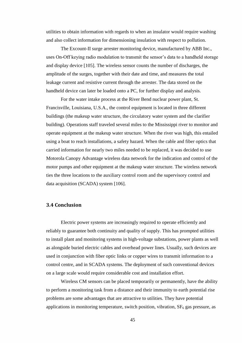
45
utilities to obtain information with regards to when an insulator would require washing
and also collect information for dimensioning insulation with respect to pollution.
The Excount-II surge arrester monitoring device, manufactured by ABB Inc.,
uses On-Off keying radio modulation to transmit the sensor‟s data to a handheld storage
and display device [105]. The wireless sensor counts the number of discharges, the
amplitude of the surges, together with their date and time, and measures the total
leakage current and resistive current through the arrester. The data stored on the
handheld device can later be loaded onto a PC, for further display and analysis.
For the water intake process at the River Bend nuclear power plant, St.
Francisville, Louisiana, U.S.A., the control equipment is located in three different
buildings (the makeup water structure, the circulatory water system and the clarifier
building). Operations staff traveled several miles to the Mississippi river to monitor and
operate equipment at the makeup water structure. When the river was high, this entailed
using a boat to reach installations, a safety hazard. When the cable and fiber optics that
carried information for nearly two miles needed to be replaced, it was decided to use
Motorola Canopy Advantage wireless data network for the indication and control of the
motor pumps and other equipment at the makeup water structure. The wireless network
ties the three locations to the auxiliary control room and the supervisory control and
data acquisition (SCADA) system [106].
3.4 Conclusion
Electric power systems are increasingly required to operate efficiently and
reliably to guarantee both continuity and quality of supply. This has prompted utilities
to install plant and monitoring systems in high-voltage substations, power plants as well
as alongside buried electric cables and overhead power lines. Usually, such devices are
used in conjunction with fiber optic links or copper wires to transmit information to a
control centre, and in SCADA systems. The deployment of such conventional devices
on a large scale would require considerable cost and installation effort.
Wireless CM sensors can be placed temporarily or permanently, have the ability
to perform a monitoring task from a distance and their immunity to earth potential rise
problems are some advantages that are attractive to utilities. They have potential
applications in monitoring temperature, switch position, vibration, SF6 gas pressure, as

46
well as the continuous voltage and current values, of virtually any HV equipment, cable,
or power line in a substation environment extending over a large area.
Wireless sensors using either the 802.11 or 802.15.4 standard are being trialed in
substation condition monitoring R&D projects, while cellular and satellite networks
have long been used for substation CM, as well as protection and control. Wireless
technologies likely to succeed as wireless data providers in the electrical substation
environments are IEEE 802.16 d/e (WiMAX), IEEE 802.11 a/b/g/n (Wi-Fi), Cellular
Networks (2G, 3G and 4G) and wireless sensor protocols that use the IEEE 802.15.4
specification like WirelessHART, International Society of Automation (ISA) 100.11a,
or Zigbee.
The very low power consumption and low data rate of 802.15.4 based wireless
sensors makes them more suited for single CM measurements, battery powered
operation. Wireless sensors based on the 802.11 modules , having large power
consumption and high data rates are more suited for multiple or even continuous CM
measurements, powered by an AC/DC mains power supply. Cellular networks, similar
to 802.11, are more suited to multiple or even continuous CM measurements, powered
by an AC/DC mains power supply.

47
Chapter 4 Design, development and functional testing of the WLAN sensor and its components
4.1 Introduction
The previous two chapters presented a background on condition monitoring for
high voltage insulators, and earth impedance measurements, as well as the varied use of
wireless sensor technologies in power system environments. In this chapter, the
components of the developed Wireless Local Area Network (WLAN) sensor are
presented.
The electronic components, which all together make up the developed WLAN
sensor, are categorized in logical themes based on their purpose and they are illustrated
in Figure 4.1. A colour scheme is used in the figure to categorize the various parts into
more basic functions like digital, analog, power electronics, or a mix of the three
functions. Each of these logical themes is described later in this chapter in more detail.
The aim of this chapter is to provide a rational behind the chosen components that make
up the logical themes and describe the specific function of each of these logical themes.
A selection of operating I/O waveforms and the functional tests performed on some of
the WLAN sensor components is also presented. The purpose of this was to verify that
the WLAN sensor‟s components operate as anticipated.
The overall purpose of the developed WLAN sensor was to be able to
continuously acquire analog data on two channels and continuously transmit that data
wirelessly. Electrical substation environments were the intended operating environment
of the WLAN sensor, with the need for a transmission distance of up to 100 m. For a
sampling rate of 80 kHz on both channels and a 14-bit ADC resolution, the data
acquisition rate would be at 560kbps. A 14-bit resolution is chosen as it is not practical
to design analog anti-aliasing filters which consist of more than 3 operational amplifiers
(6-pole low-pass filters).

48
Figure 4.1: WLAN sensor block diagram.
The average wireless transmission rate would be higher, which would depend on
the wireless technology used and the wireless transmission error rate. As more wireless
sensors might operate as part of the same wireless monitoring network, the average
permissible wireless data rate per network would have to be large. The order of which
would be many tens of Mbps. The 802.11g technology, having a practical wireless data
rate of 30 Mbps [60, 63], was chosen to perform the wireless communication duties for
the WLAN sensor. While 802.11 modules provide a high wireless data rate for
communication, they also require more power when compared to 802.15.4 or 802.15.1
modules.
For the given sampling rate and ADC resolution, a 16-bit fast microcontroller
was chosen. The microcontroller processing speed of 40 MHz was considered adequate
and removed the need to move to faster Digital Signal Processors (DSP) ICs or more
complex Field Programmable Gate Arrays (FPGA) and microcontroller hybrid designs.
The maximum power consumption of the chosen microcontroller, running at its
maximum operating speed, was anticipated to be in the few hundreds of mWs region. A
parallel memory IC was chosen based on its fast speed and adequate storage size of at
least 1 second worth of acquired data.
As the need for the WLAN sensor was to measure AC signals on two channels,
with a 14-bit resolution and a sampling rate of at least 80 kHz, a two channel bipolar, ±5
V, 500 kHz, ADC was chosen. While the onboard ADC of the microcontroller could
have been used, making this choice removed the need for the extra level shifting and
attenuating circuitry required to interface an AC signal to a unipolar ADC [94].

49
Two low-pass filters per channel were required for anti-aliasing purposes. These
active filters would use multiple operational amplifiers for their needs. A buffering op-
amp would be required before the beginning of each of the filter circuitry. The purpose
of the buffering op-amp would be to isolate the impedance of the physical sensor
(/transducer) from that of the anti-aliasing filter. Surge protection components would be
required in the WLAN sensor design to sufficiently attenuate any signal larger than
about ±5 V.
As the analog anti-aliasing filters would still allow some aliased signals through
a four point moving average filter would also have to be used. A moving average is type
of Finite Impulse Response (FIR) filter whose function if viewed simplistically can be
regarded as smoothing the data or as a digital low-pass filter. Its usefulness to the
WLAN sensor and DAQ card data is to remove any aliased data within the 10 – 40 kHz
range, that the analog anti-aliasing filter could not remove. A moving average filter is
also relatively ease to implement and will require very little processing time as long as
the averaging number is the square of two.
A solar battery powered approach was chosen as the power supply for the
WLAN sensor. This would allow the WLAN sensor to operate were mains power is not
available. High energy storage lithium ion batteries would be used so that the WLAN
sensor could operate during the night. Efficient switching regulators would be used to
convert the battery voltage to that required by each individual IC. Finally the
microcontroller would control the power supplied to the 802.11‟s WLAN sensor
module via a MOSFET.
In this chapter, the details of the 802.11 module used as the wireless transceiver
of the wireless sensor is presented first. The microcontroller which was used to receive
wirelessly transmitted commands that controls the data acquisition process, process the
acquired data and also transmits acquired data is then described. The surge protection
components are presented next, followed by the low-pass filters and the Analog-to-
Digital Converter (ADC). The description of the switching voltage regulators used by
the wireless sensor are next presented and finally the solar Maximum Power Point
Tracking (MPPT) battery charger is presented. All electronic circuit schematics that
make up the wireless sensor are shown in Figures A.1, A.2, A.3, A.4, A.5, A.6 and A.7
in Appendix A. The Bill of Material (BOM) tables that contain a list of all the
components used which make up the wireless sensor, are summarized in Tables A.1,

50
A.2 and A.3 in Appendix A. The WLAN sensor is made up of 156 components having
cost a total of £392.367 in the year of their purchase.
4.2 The Lantronix Matchport IEEE 802.11b/g wireless module
The MatchPort MP1002000G-01, as depicted in Figure 4.2, was used as the
wireless transceiver of the developed WLAN sensor. The Matchport 802.11 module
removes the complexity of converting the acquired data into Transmission Control
Protocol/Internet Protocol (TCP/IP) packets and then into 802.11 packets. The 802.11
module uses its Universal Asynchronous Receiver Transmitter (UART) module to
receive data, which it then converts into TCP/IP packets and finally into 802.11 packets,
ready for wireless transmission. The opposite is true for wireless packets destined for
the Matchport 802.11 module. A data packet destined for the Matchport 802.11 module
is converted from an 802.11 packet into a TCP/IP packet and the data content of the
wireless packet is finally converted into a series of bytes ready to be transmitted to the
microcontroller, via the Matchport‟s UART port. The Matchport module supports the
802.11i security standard, with 256-bit AES encryption for true secure data transfer.
The Matchport module can have a range of data rates up to a maximum of 921.6 kbps.
The maximum wireless (802.11) data rate of the module is 54 Mbps, and was measured
using a Fluke 155 „True RMS‟ multimeter, to have a maximum power consumption of
1.023 W with a supply voltage of +3.3 V. This particular 802.11 module was chosen as
the communication transceiver due to its high data rate, ease of interfacing to the
microcontroller and its well documented data sheets.
Figure 4.2: Matchport b/g - Embedded Wireless Device. Reproduced from [107].

51
4.3 Operation of the PIC24HJ256GP210 microcontroller
4.3.1 Introduction
A Peripheral Interface Controller (PIC) microcontroller has the advantage of
being a complete computer in a single integrated circuit (IC) package. The only external
components necessary are whatever is required by the I/O devices that are connected to
the PIC. The PIC24HJ256GP210 was the microcontroller used in the wireless sensor. It
has a 16kb of RAM memory, and its Central Processing Unit (CPU) offers 16-bit data
and 24-bit address paths, while its speed was set to its maximum speed of 40MHz. The
supply voltage of the microcontroller is +3.3 V.
In order for microcontrollers to achieve a fast exchange of information with
other I/O devices and to be able to detect and respond quickly to physical events that are
taking place, dedicated architecture is contained within them. This architecture is
divided into logical divisions, generally known as peripherals, which can be accessed by
the microcontroller when needed. These peripherals can be one or more ADCs, DACs,
Pulse Width Modulators (PWM) and a number of different wired digital communication
peripherals like Inter-Integrated Circuit (I2C), Serial Peripheral Interface (SPI) and
UART. The PIC24HJ256GP210 has a number of these built-in peripherals, but only
those that were used in the operation of the wireless sensor are discussed in this chapter.
4.3.2 Interrupts and timers
The microcontroller timer has the role of a counter that triggers an action when
its count reaches a particular value. The PIC24HJ256GP210 has nine 16-bit timers,
which can also be combined to create eight 32-bit Timers.
In order to implement efficient input/output operations for the developed
microcontroller-based wireless sensor, interrupts are of critical importance. An interrupt
in the microcontroller allows a forced deviation from normal program flow by an
external or internal event. The PIC24 has many possible internal and external events
such as rising and falling edges on external pins, arrival of serial data, timer expiration
and so forth, that can cause interrupts.
The code that is executed when the interrupt occurs is referred to as the Interrupt
Service Routine (ISR). The ISR‟s function is to respond to the signal or event that

52
triggered the interrupt. As an example, if the interrupt was triggered by the need to send
data through the UART, the ISR would send data to the UART‟s transmit buffer.
However, the ISR is never manually called, as a normal C function is called. Instead,
the ISR is invoked automatically by the PIC24 interrupt hardware on an interrupt
occurrence. An ISR is said to execute in the background while the normal program flow
executes in the foreground.
4.3.3 Serial peripheral interface
The Serial Peripheral Interface (SPI) is a three, or more commonly four wire
synchronous serial link, originally developed by Motorola. The SPI is a full duplex
communication channel that uses one pin for receiving data one for transmitting, one for
the clock and one for selecting a device. The SPI was programmed to have a maximum
data rate of 1,250kbps and communicate in 16-bit long packets. The microcontroller in
the wireless sensor uses its SPI port to receive data from the external bipolar ADC, as
shown in Figure 4.3.
Figure 4.3: SPI port linking the ADC to the microcontroller.
The SDI2 line is the one transmitting the acquired data to the microcontroller for
processing, while the SS2 line forces the ADCs SPI port to „wake up‟ and start
transmitting data. The digital clock is transmitted by the microcontroller on the SCK2
line, which is used by the ADC to synchronize the transmission of its data. The CNVST
line is used by the microcontroller to force the ADC to sample data and it can also be
used to shut down the ADC. Once the sampling of data has taken place, the ADC‟s
BUSY line will trigger an interrupt routine in the microcontroller so that it can
immediately read the acquired data.

53
4.3.4 Universal asynchronous receiver transmitter (UART)
The Universal Asynchronous Receiver Transmitter (UART) module is one of
the serial I/O modules available in the PIC24. The UART is a full duplex asynchronous
communication channel that has a 4-deep First-In First-Out (FIFO) transmit and receive
data buffer. The PIC24‟s UART, as shown in Figure 4.4, was set to its maximum data
rate of 921 kbps, 8 data bits, one parity bit and one stop bit. The UART hardware
module was enabled to generate interrupts when data transmission or data reception
occurred. This crucial hardware part for efficient UART operation using Interrupt
Service Routines (ISRs) is further discussed in Chapter 5.
Figure 4.4: UART port linking the 802.11 module to the microcontroller.
The microcontroller uses its UART port to transmit processed data acquired by
the ADC, to the Matchport b/g module, while also receiving wirelessly transmitted
commands from it. With reference to Figure 4.4, the U2RX line moves data from the
Matchport module to the microcontroller, while the U2TX line transmits data from the
microcontroller to the Matchport module. The U2RTS (Request-To-Send) line is used
by the microcontroller to inform the Matchport module that it would like to transmit
data to it, while the U2CTS (Clear-To-Send) line informs the microcontroller that it can
send data. Data sent by the Matchport module will trigger an interrupt routine so that
the microcontroller can immediately read the incoming data.

54
4.3.5 Input/Output ports
The PIC24 microcontroller has a number of digital input and output ports that
can be used for a variety of purposes. Pin 38 of the PIC24HJ256GP210, as shown in
Figure 4.5, was used to set and clear the gate pin of the p-channel IRF7707PBF Metal
Oxide Field Effect Transistor (MOSFET). If the gate pin of the MOSFET was high (3.3
V), then current can flow from the source to drain. If, on the other hand, the gate pin
was low (0 V), the no current can flow from the source pin to the drain. This simple
circuit, as seen in Figure 4.5, was used to remove power from the Matchport module at
the will of the microcontroller. The On resistance of the MOSFET is 0.03 Ω [108].
Figure 4.5: Microcontroller digital output port controlling power to the 802.11
module via a MOSFET.
The charge pump IC MCP1253-33X50 [109] was used to step up the voltage
from +3.3 V to +5 V for the needs of the filtering operational amplifiers and the ADC.
In order to be able to shutdown the MCP1253-33X50 and reduce the power
consumption when needed, the digital output port on pin 17 of the microcontroller was
connected to pin7 of the charge pump, as shown in Figure 4.6. A high signal (3.3 V) on
pin 7 of the charge pump turns it on, while a low signal (0 V) shuts it down. The 10 kΩ
resistor to ground was used to set the default state of the charge pump to be OFF.
Figure 4.6: Microcontroller digital output pin controlling power to the MCP1253-
33x50 charge pump.
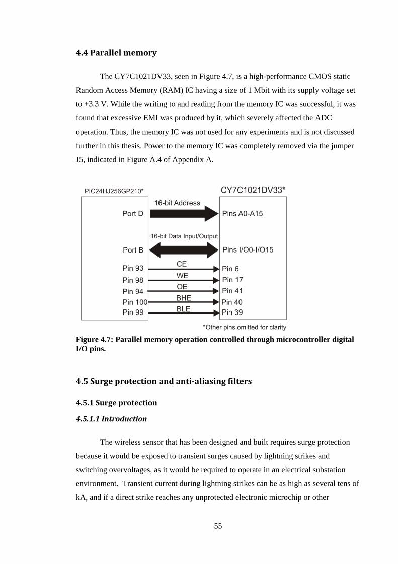
55
4.4 Parallel memory
The CY7C1021DV33, seen in Figure 4.7, is a high-performance CMOS static
Random Access Memory (RAM) IC having a size of 1 Mbit with its supply voltage set
to +3.3 V. While the writing to and reading from the memory IC was successful, it was
found that excessive EMI was produced by it, which severely affected the ADC
operation. Thus, the memory IC was not used for any experiments and is not discussed
further in this thesis. Power to the memory IC was completely removed via the jumper
J5, indicated in Figure A.4 of Appendix A.
Figure 4.7: Parallel memory operation controlled through microcontroller digital
I/O pins.
4.5 Surge protection and anti-aliasing filters
4.5.1 Surge protection
4.5.1.1 Introduction
The wireless sensor that has been designed and built requires surge protection
because it would be exposed to transient surges caused by lightning strikes and
switching overvoltages, as it would be required to operate in an electrical substation
environment. Transient current during lightning strikes can be as high as several tens of
kA, and if a direct strike reaches any unprotected electronic microchip or other

56
component, it may cause their complete breakdown. Given the magnitude of currents
involved, without surge protection, the whole wireless sensor could easily be destroyed
by lightning strikes or switching overvoltages.
Surge protection diverts the excess energy from the transient overvoltage away
from the wireless sensor into the ground. It is therefore vital for a surge protection
device to have a high quality ground connection to safely shunt away the unwanted
energy from the transient into ground. Three stage surge suppression was chosen for the
wireless sensor. The three devices chosen are a Gas Discharge Tube (GDT), a Metal
Oxide Varistor (MOV) and Transient Voltage Suppressor (TVS).
Three-stage surge protection uses the three components to provide effective
protection to the wireless sensor against transients. This protection is achieved through
placing the three components in a specific order. This order is the GDT first, followed
by the MOV and finally the TVS.
The GDT is first because it is slow reacting and requires relatively large voltages
to begin conduction, but it can also shunt very large currents to ground. GDTs consist
of two electrodes parallel to each other in a sealed ceramic case filled with a mixture of
noble gases. GDTs are designed to be insulating under normal voltage and current flow
but when under transient surges or spikes, the two metal electrodes are shorted by an arc
discharge between them, which creates a plasma breakdown of the noble gases within
the gas tube. In this plasma state, the gas tube becomes a conductor and essentially
short circuits, thus protecting the system from any damage from the transient.
Compared with solid state conductors such as the TVS and the MOV, GDTs can shunt a
much higher current to ground. The chosen GDS component is the A80-A75XSMD
manufactured by EPCOS, which begins conducting current at 75V.
The second stage of the three-stage surge suppressor is the MOV which is made
up of conducting zinc oxide grains mixed with a blend of rare earth additives. The
MOV has a high resistance at low voltages or under normal operating conditions and a
low resistance at high voltages such as when a transient surge or spike is applied to it.
The chosen MOV component is the VE17M00140K manufactured by AVX, which
begins conducting current at 14V.
The final device, the TVS, is a semiconductor device that has been specifically
designed to provide protection against transients. The TVS is the component that will be
first to begin conducting current away from the sensitive electronic components of the
wireless sensor. The chosen TVS component is the SMCG5.0CA-E3/57T manufactured
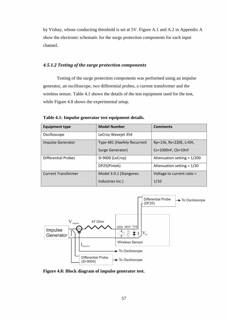
57
by Vishay, whose conducting threshold is set at 5V. Figure A.1 and A.2 in Appendix A
show the electronic schematic for the surge protection components for each input
channel.
4.5.1.2 Testing of the surge protection components
Testing of the surge protection components was performed using an impulse
generator, an oscilloscope, two differential probes, a current transformer and the
wireless sensor. Table 4.1 shows the details of the test equipment used for the test,
while Figure 4.8 shows the experimental setup.
Table 4.1: Impulse generator test equipment details.
Equipment type Model Number Comments
Oscilloscope LeCroy Wavejet 354
Impulse Generator Type 481 (Haefely Recurrent
Surge Generator)
Rp=15k, Rs=220E, L=0H,
Cs=1000nF, Cb=10nF
Differential Probes SI-9000 (LeCroy) Attenuation setting = 1/200
DP25(Pintek) Attenuation setting = 1/20
Current Transformer Model 3-0.1 (Stangenes
Industries Inc.)
Voltage to current ratio =
1/10
Figure 4.8: Block diagram of impulse generator test.

58
Figure 4.9 show the measured voltage and current impulse waveshapes before they
reach the surge protection of the wireless sensor. A small offset error is visible on the
impulse current waveform in Figure 4.9. This is believed to be an oscilloscope offset
error of about 10mV magnitude (or 100mA Impulse Current magnitude). Figure 4.10
shows the voltage impulse waveshape after the impulse has been reduced by the three
surge protection components. The reduction seen after the surge protection components
is considerable, starting with an impulse of 100V and clamping it down to little over
10V. However given that the operational amplifiers data sheet requires no larger swings
than +/-5.3V [110], more surge protection or even galvanic isolation might be
necessary. While more attenuation would be required for, the TVS which is the fastest
device begins to conduct current at 5V. It was, thus, expected that the operational
amplifiers lower and upper voltage input limits would be exceeded by a certain margin.
Figure 4.9: Measured impulse voltage and current applied to the wireless sensor
through a 47 Ω resistor.

59
Figure 4.10: Measured impulse voltage after surge protection components.
4.5.2 Chopper stabilized operational amplifiers
Operational amplifiers have a number of specifications including cost, power
consumption, offset, offset drift, open-loop gain, bandwidth, slew rate and distortion.
An op amp had to be chosen for use in the low pass anti-aliasing filter, which would be
driving an ADC. Given that no need for signal amplification was required, the relative
low sampling speed of the wireless sensor and the fact that large or small amplitude
bipolar signals were to be measured, a low offset op amp was needed. For low offset
and drift performance, chopper stabilized amplifiers are considered to be one of the best
choices. Thus, two LTC2052 quad packages, zero-drift operational amplifier were
chosen; one for each analog input channel. It can support +/-5V rail-to-rail operation,
has a maximum offset of 3µV and a power consumption of 750μA per op amp.
4.5.3 Anti-aliasing filters
Filters are used to separate signals, passing those of interest and attenuating the
unwanted frequencies. In data conversion, filters are used to eliminate the effects of
aliases in the analog to digital conversion process.

60
The five parameters of a practical filter are defined in Figure 4.11.
Figure 4.11: Key filter parameters. Reproduced from [111].
The cutoff frequency (Fc) is the frequency at which the filter response leaves the error
band (or -3dBpoint for a Butterworth response filter). The stop band frequency (Fs) is
the frequency at which the minimum attenuation in the stop band is reached. The pass
band ripple (Amax) is the variation (error band) in the pass band response. The minimum
pass band attenuation (Amin) defines the minimum signal attenuation within the stop
band. The steepness of the filter is defined as the order (M) of the filter [111].
The Sallen-Key is one of the most widely used filter topologies and can be seen
in Figure 4.12. One reason for its popularity is that this configuration shows the least
dependence of filter performance on the performance of the operational amplifier [111].
Figure 4.12: Sallen-Key low pass filter.

61
In the design of the wireless sensor one low pass filter was implemented on each
channel. A buffering op-amp on each channel, for impedance isolation between the
transducer and low pass filter was used. The 14-bit ADC AD7367-5 described in the
section below has a Signal-to-Noise+Distortion (SINAD) value of 75 dB. The designed
low pass filter would be necessary to filter all signals with the cut-off frequency starting
at 10 kHz and an attenuation of 75 dB before it reached the stop band frequency of 40
kHz (or half the sampling frequency of the ADC Nyquist frequency).
The LTC2052 quad op-map IC was used on each channel for buffering and
filtering. One op-amp was used for buffering and the rest were designed into a 6th
pole
low-pass filter. A Butterworth type filter was chosen since it is the best compromise
between attenuation and phase response. It has no ripple in the pass band or the stop
band, and because of this, it is sometimes called the maximally flat filter. The values of
the elements of the Butterworth filter are more practical and less critical than many
other filter types. The theoretical amplitude response against normalized frequency of a
6th
order Butterworth filter is reproduced in Figure 4.13. Its design table is given in
Table 4.2.
Figure 4.13: Butterworth amplitude response against frequency. Reproduced from
[111].
6th
order filter response

62
For a 6th
order Butterworth low-pass filter realized using a Sallen-Key topology,
the underlying equations given in [111] are:
(4.1)
(4.2)
(4.3)
(4.4)
(4.5)
(4.6)
where C1 and R3 are values chosen beforehand. Since no gain was used, resistors R3 and
R4 are not part of the filter.
Table 4.2: 6th
order Butterworth design table. Reproduced from [111].
Order Section F0 a Q
6 1 1.000 1.9319 0.5176
2 1.000 1.4142 0.7071
3 1.000 0.5176 1.9319
Solving the above equations, the closest real values for the resistors (1%
accuracy) and capacitors (5% accuracy) were chosen based on the theoretical calculated
values. Table 4.3 shows the chosen values, and Figure 4.14 illustrates the circuit
schematic of buffering op-amp and 6th
order Sallen-Key filter. The wireless sensor has
two channels with identical filters. Figures A.1 and A.2 of Appendix A show the full
electronic circuit schematics for the two channels.
Table 4.3: 6th
order Butterworth resistor and capacitor values.
Reference Resistor Value (Ω) Capacitor Value (F)
R1,R2 16.5 k, 16.5 k
C1, C2 1 n, 820 p
R3, R4 22.6 k, 22.6 k
C3, C4 1 n, 510 p
R5, R6 61.9 k, 61.9 k
C5, C6 1 n, 68 p

63
Figure 4.14: Buffering op-amp and 6th
order Butterworth filter.
A Farnell LF1 sinewave generator along with a LeCroy Wavejet 354
oscilloscope with were used to measure the response of the wireless sensors anti-
aliasing filters. A 1 V peak-to-peak sinewave was injected into the filters, starting with
frequencies from 50 Hz and up to 40 kHz. The measured amplitude response against
frequency curves can be seen in Figure 4.15.
Figure 4.15: Measured Butterworth filter amplitude response against frequency
curves.
The expected attenuation in Figure 4.15 would have been -70 dB at 40 KHz while the
measured attenuation was only -26 dB. This discrepancy is believed to be because of the

64
parasitic capacitances of the custom made printed circuit board on which the filters
components were soldered.
4.6 Analog-to-digital converters
Due to the bipolar nature of the signals that would be measured, the AD7367-5
ADC was chosen for use in the wireless sensor. It is a bipolar, dual, 14-bit, low power,
successive approximation analog-to-digital converter (ADC) that features conversion
rates up to 500 ksamples/sS. The AD7367-5 device contains two ADCs, which are both
preceded by a 2-channel multiplexer (MUX) and a low noise, wide bandwidth, track-
and-hold (T/H) amplifier, as can be seen in Figure 4.16.
Figure 4.16: Functional block diagram of AD7367-5, Reproduced from [112].
Control of the ADC is made through its CNVST and BUSY pins, as described in
section 4.3.3, while transmission of the acquired data is done via its SPI port using 16-
bit word. Both of the ADC‟s channels were set up as single ended inputs and can accept
bipolar inputs in the range of ±5 V, on both of its channels. Figure A.5 of Appendix A

65
shows the electronic circuit schematic for the AD7367-5. The ADC requires multiple
supply voltages of ±5V and +3.3 V.
4.7 Switching voltage regulators
4.7.1 Introduction
A number of components in the wireless sensor require different supply voltage
to operate. The microcontroller, the external bipolar ADC and the WLAN Tx-Rx
through the MOSFET, all require +3.3V to operate. In addition, the external bipolar
ADC requires +5V and -5V to operate correctly. The low pass active filters also require
+5V and -5V. Figure 4.17 shows a block diagram representation of the different supply
voltages across the wireless sensor.
Figure 4.17: Block diagram showing supply voltages across the wireless sensor.
Power supplied to the +3.3V switching regulator (LT1933) is provided by the lithium
ion batteries/ Solar MPPT battery charger (LT3652), which is further discussed in
section 4.8. The +3.3V switching regulator (LT1933) also supplies power to the +5V
step up regulator (MCP1253-33X50). The +5V step up regulator (MCP1253-33X50) its
turn, supplies power to the -5V inverting regulator (TC1121). It should be pointed out
that if power is removed from the +5V step up regulator (MCP1253-33X50), as

66
discussed in section 4.3.5, power will also be removed from the -5V inverting regulator
(TC1121). The outputs from the Solar MPPT battery charger (LT3652), the lithium ion
batteries and the input to the +3.3V switching regulator (LT1933) are all at the same
potential.
4.7.2 Step down switching regulator
Figure 4.18 shows a simplified circuit diagram of a voltage step-down or „buck‟
circuit. When the switch closes the input, voltage appears at the inductor. Current
flowing through the inductor/capacitor combination builds over time.
Figure 4.18: Conceptual Feedback Controlled Step-Down Regulator. Reproduced
from [113].
The operation of a step down converter is probably best described as:
“When the switch opens current flow ceases and the magnetic field around the
inductor collapses. The voltage induced by the collapsing magnetic field is opposite to
the originally applied voltage. As such, the inductor’s left side swings towards negative
and is clamped by the diode. The capacitor’s accumulated charge has no discharge
path and a DC potential appears at the output. This DC potential is lower than the input
because the inductor limits current during the switch’s on-time. Ideally, there are no
dissipative elements in this voltage step-down conversion. Although the output voltage
is lower than the input, there is no energy lost in this voltage-to-current-to-magnetic
field-to-current-to-charge-to-voltage conversion. In practice, the circuit elements have
losses but step-down efficiency is still much higher than with inherently dissipative
approaches like resistive voltage dividers” [113].

67
The LT1933, used in the wireless sensor, is a current mode Pulse Width
Modulation (PWM) step-down DC/DC converter with a maximum output current of
500 mA. It operates at a fixed switching frequency of 500 kHz and supplies a voltage of
+3.3 V from the varying voltage of 5.6-8.4 V. Figure 4.23 shows the voltage supplied
by the MPPT/battery charger is converted to 3.3 V, which then supplies the
microcontroller, matchport b/g wireless transceiver, ADC and charge pump. The +3.3 V
supply was measured using a LeCroy Wavejet 354 oscilloscope and can be seen in
Figure 4.19. Figure A.6 of Appendix A shows the electronic circuit schematic for the
LT1933 regulator.
Figure 4.19: Waveform showing the +3.3V supply measured at the output from the
LT1933 regulator.
4.7.3 Switched-Capacitor Voltage Converters
A switched-capacitor (or charge pump) is an electronic circuit that uses
capacitors as energy storage elements to create either a higher or lower voltage power
source. Charge pump circuits, as shown in Figure 4.20, are capable of high efficiencies,
sometimes as high as 90-95% while being electrically simple circuits. Charge pumps
use some form of switching device to control the connection of voltages to the
capacitor, and the charge pumping action typically operates at tens of kilohertz up to

68
several megahertz to minimize the amount of capacitance required. The output voltage
from a switched-capacitor converter is load-dependent and higher loads result in lower
average output voltages.
Figure 4.20: Simplified circuit diagram of a switched capacitor. Reproduced from
[114].
Given the need for +/-5V supply required by the low pass filters and ADC, two
charge pump DC/DC regulators were chosen. One was used for positive and one for
negative voltage regulation.
The MCP1253-33X50 is an inductorless, positive-regulated charge pump
DC/DC converter. It is specifically designed for applications requiring low noise and
high efficiency and is able to deliver up to 120 mA output current. The MCP1253 has a
switching frequency of 1 MHz and generates a regulated, fixed 5.0 V output voltage.
The TC1121 is a charge pump converter with 100 mA output current capability.
It converts a 2.4-5.5V input to a -5V output voltage. As with all charge pump
converters, the TC1121 uses no inductors, saving cost, size and reducing potential EMI.
The power to the MCP1253-33X50 is supplied at a 3.3V supply voltage. The
positive-regulated charge pump then converts that voltage to +5V, which is used to
supply the op amps, ADC and negative-regulated charge pump. The TC1121 converts
the +5V input to -5V output. As the output voltage from the charge pumps is load-
dependent and higher loads result in lower average voltages, both charge pumps were
chosen based on their ability to supply many orders of magnitude more current than
would be required. This was done in order to ensure that the precise supply voltage was
produced for the op amps and ADC. The ±5V supplies were measured using a LeCroy
Wavejet 354 oscilloscope and can be shown in Figure 4.21. Figure A.6 of Appendix A

69
shows the electronic circuit schematics for the MCP1253-33X50 and TC1121 charge
pumps.
(a) +5 V supply
(b) -5 V supply
Figure 4.21: Waveforms showing the +5 V (a) and -5 V(b) supplies measured at the
outputs of the MCP1253 and TC1121 regulators.
4.8 Solar powered lithium ion battery charger
4.8.1 Description of the solar powered battery charger

70
Nearly all solar-powered devices contain rechargeable batteries as solar power
availability varies greatly daily and seasonally. The goal is to extract as much solar
power as possible to charge the batteries quickly and maintain their charge. Solar cells
are inherently inefficient devices, but they do have a point of maximum power output,
so operating at that point seems an obvious design goal. The problem is that the output
current versus voltage characteristic of a solar panel changes with solar irradiance.
Maximum power output for a given solar irradiance occurs at the knee of each I-V
curve, as can be seen in Figure 4.22, where the cell changes from a constant voltage
device to a constant current device [115]. A battery charger design that efficiently
extracts power from a solar panel must be able to steer the panel‟s output voltage to the
point of maximum power when illumination levels cannot support the charger‟s full
power requirements.
Figure 4.22: I-V and power curves for a solar panel. Curves in red colour show the
output power from the panel for a number of irradiance magnitudes (in W/m2).
Reproduced from [115].
The LT3652 employs an input voltage regulation loop that reduces the charge
current if the input voltage falls below a programmed level set by a simple voltage
divider network. When powered by a solar panel, the input voltage regulation loop is
used to maintain the panel at near peak power output.
The LT3652 was used in the wireless sensor as the maximum power point
tracking regulator for the solar panel and as the lithium ion battery charger. Power from

71
the solar panel was drawn by the LT3652 to charge two pairs of lithium ion batteries in
series, as shown in Figure 4.23.
Figure 4.23: Block diagram showing power flow from solar panel, through the
LT3652 and into the batteries and voltage regulator.
Solar power is common for powering wireless networks, and many devices have
been proposed in the literature [116, 117]. The MSX-20, 462 mm x 501 mm
semicrystalline silicone solar panel, in conjunction with the lithium ion batteries, was
selected as the main energy harvesting unit. Under standard irradiance and temperature
conditions (1 kW/m2, 25°C), the panel typically generates 20 W peak power, with an
output voltage of 16.8 V and a current of 1.19 A. The choice of the solar panel was
made based on its large power output which would be able to continuously power the
WLAN sensor during summer daylight hours. For the WLAN sensor to operate
throughout any given day of the year, the solar panel and battery sizes would have to be
dimensioned accordingly.
The battery charger is a Linear Technology LT3652 monolithic step-down
(buck) converter IC. The charger incorporates a Maximum Power Point Tracking
(MPPT) algorithm to optimize power output under varying irradiance conditions, while
at the same time varying the output voltage between 5.6 V and 8.4 V, according to the
operational requirements of the battery. The battery pack consists of an array of four 2.6
Ah rechargeable lithium ion batteries (Cylindrical, Type: 18650, Tenergy Corp.), each
with normal operating range between 2.8 V and 4.2 V. These batteries have high-energy
density and a long discharge time constant. When fully charged, the batteries allow the
WLAN sensor to transmit data continuously for 19 hours, with the advantage of being
recharged whenever required, irrespective of the amount of charge in the batteries. Each
battery also contains an internal voltage protection printed circuit board, which is
72
typical for Li-ion batteries. Figure A.7 of Appendix A shows the electronic circuit
schematic for the LT3652 MPPT battery charger.
4.8.2 Solar laboratory test arrangement
The LT3652 MPPT battery charger was tested using the halogen-tube array solar
test facility at Cardiff University, shown in Figure 4.25. All 36 halogen-tube lamps were
turned on for the test. For this experiment, the solar panel was placed horizontally on
the floor of the solar laboratory, and solar irradiance at the center of the panel was
measured to be 610 W/m2, using a CM3 Kipp&Zonen pyronometer.
For completely discharged batteries, the solar panel‟s voltage and current
outputs, as well as the Lithium-ion batteries voltage and current values were measured
using four Fluke 155 „True RMS‟ multimeters. Figure 4.24 shows the test diagram for
the solar battery charging test. Measurements values from the multimeters were
recorded manually every 10 minutes.
Figure 4.24:Test diagram for solar battery charging test.
1: Solar panel, 2: Voltage meter, 3: Current meter, 4: LT3652 MPPT Battery
Charger, 5: Lithium Ion Batteries, 6: Current meter, 7: Voltage meter, 8: LT1933
Voltage regulator.

73
During the test, the WLAN sensor has its wireless module, ADC, filters, +5V
and -5V regulators programmatically turned off. The power consumption of the WLAN
sensor in this state was measured to be 0.288W. The maximum power consumption of
the WLAN sensor during data acquisition and wireless transmission was measured to be
2.1W.
The purpose of the test was to measure the voltage and current profiles of the
charging batteries and contrast it with typical lithium ion batteries V-I profiles. The
solar panel‟s voltage and current profiles were also measured to identify whether the
LT3652 was actually performing maximum power point tracking.
Figure 4.25: Halogen-tube array solar test facility at Cardiff University.
4.8.3 Test Results
The measured solar panel and Li-Ion batteries voltage and current profiles
against time are shown in Figure 4.26 and Figure 4.27. From Figure 4.26 it can be seen
that the LT3652 does perform maximum power point tracking by regulating the voltage
and current magnitudes at which it draws power from the solar panel. The LT3652
begins to draw power from the solar panel at 16 V, which corresponds well with the
Vmpp for a moderately lit solar panel. As the test progresses and the batteries charge up,

74
less current is needed from the solar panel. Thus, the LT3652 slowly moves away from
the Vmpp to a higher voltage value. The measured voltage and current profile of the
charging Li-ion batteries are comparable to typical ones seen in Figure 4.28. The
battery‟s voltage increases rapidly, while the charging current remains relatively
constant. Within 3 hours the charging current begins to decrease, while the charging
voltage gradually increases.
Figure 4.26: Measure solar panel voltage and current profiles.
Figure 4.27: Measured lithium-ion batteries voltage and current profiles.
Vin
Iin
Ibat
Vbat

75
Figure 4.28: Lithium-ion battery charging profile. Reproduced from [53].
Figure 4.26 and Figure 4.27 provide as with a typical lithium ion battery
charging profile during a summer day in Cardiff, UK for the WLAN sensor. Further
tests in the solar laboratory should take place to better characterize the operation
(efficiency vs. irradiance, charging time vs. irradiance) of the battery charging circuitry
of the WLAN sensor for a range of irradiance values (0.1 – 1 kW/m2).
The operation of the battery charging circuitry could be further investigated with
the addition of a battery monitoring IC. While this would require the WLAN sensors
redesign, such an IC could provide a continuous data stream of the capacity of the
battery over large time periods for laboratory or outdoor environments.
4.9 Printed circuit board design and manufacture
The design of the wireless sensor Printed Circuit Board (PCB) was made using
Proteus PCB Design software package which contains the ISIS Schematic Capture
software and the ARES PCB Layout software. All of the microchips, resistors,
capacitors, inductors, LEDs that make up the wireless sensor were first designed into
the ISIS Schematic Capture software.
ISIS Schematic Capture software is responsible for the drawing appearance of
components as well as the electrical connection between components and the

76
components physical dimensions. Figures A.1, A.2, A.3, A.4, A.5, A.6 and A.7 of
Appendix A show the electronic circuit schematic output files of the wireless sensor,
produced in ISIS.
The ARES PCB Layout software uses the information available in the electronic
schematic files and allows the user to design the physical PCB. The physical
components were placed one by one, on a defined 100 mm x 160 mm 2D area in ARES.
Each component‟s pin was appropriately connected, as guided by ARES.
The produced top and bottom masks of the PCB were then printed on JetStar
Premium film using a high resolution inkjet printer. A double side pre-coated positive
photoresist fibreglass (FR4) PCB, with dimension of 100 mm x 160 mm, was placed
between the printed masks. The masks and PCB were then exposed to Ultra Violet (UV)
light in an AZ Double Sided UV Vacuum Unit for 1 minute. After the UV exposure, the
PCB was removed from between the masks and was then developed using Sodium
Metasilicate Pentahydrate, for 10 seconds. The PCB was then etched using Ferric
Chloride, in a PA310 Tri-Tank Unit for 30 minutes. Finally, the PCB‟s through holes
were drilled.
Solder paste CR44 (Edsyn GMBH Europa) that has a melting temperature of
183°C, was placed on the pads of the components. Excess solder was removed from the
pads and the components were accurately placed onto their pads. The PCB was then
placed on a Reflow Hot Plate (Golf Flow, Model: GF-SL, APS Inc.), set at 200° C, for
90 seconds. Figure 4.29 shows a photograph of the custom made PCB along with its
lithium ion batteries, aluminium enclosure, antenna and solar panel.

77
Figure 4.29: Photograph of the WLAN sensor with its lithium ion batteries,
aluminium enclosure and solar panel.
4.10 Conclusion
A WLAN sensor was designed, built and tested. The operation of the
microcontroller, ADC, wireless transceiver and switching regulators was explained. The
operation of the surge protection components was tested and considered acceptable. The
anti-aliasing filters were also tested and their operation is thought to require
improvement. Finally, the solar powered lithium-ion battery charger IC was tested in a
laboratory condition and was found to follow its published operation. Such an energy
scavenging method was considered suitable for wireless sensors.
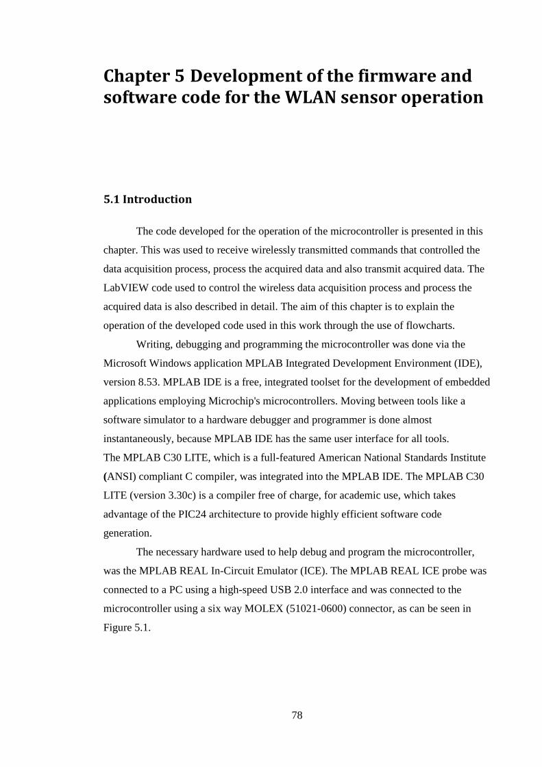
78
Chapter 5 Development of the firmware and software code for the WLAN sensor operation
5.1 Introduction
The code developed for the operation of the microcontroller is presented in this
chapter. This was used to receive wirelessly transmitted commands that controlled the
data acquisition process, process the acquired data and also transmit acquired data. The
LabVIEW code used to control the wireless data acquisition process and process the
acquired data is also described in detail. The aim of this chapter is to explain the
operation of the developed code used in this work through the use of flowcharts.
Writing, debugging and programming the microcontroller was done via the
Microsoft Windows application MPLAB Integrated Development Environment (IDE),
version 8.53. MPLAB IDE is a free, integrated toolset for the development of embedded
applications employing Microchip's microcontrollers. Moving between tools like a
software simulator to a hardware debugger and programmer is done almost
instantaneously, because MPLAB IDE has the same user interface for all tools.
The MPLAB C30 LITE, which is a full-featured American National Standards Institute
(ANSI) compliant C compiler, was integrated into the MPLAB IDE. The MPLAB C30
LITE (version 3.30c) is a compiler free of charge, for academic use, which takes
advantage of the PIC24 architecture to provide highly efficient software code
generation.
The necessary hardware used to help debug and program the microcontroller,
was the MPLAB REAL In-Circuit Emulator (ICE). The MPLAB REAL ICE probe was
connected to a PC using a high-speed USB 2.0 interface and was connected to the
microcontroller using a six way MOLEX (51021-0600) connector, as can be seen in
Figure 5.1.

79
Figure 5.1: Schematic diagram for debugging and programming of the
microcontroller. Adapted from [118].
A Category 5 cable (CAT5) is used via a high speed, noise tolerant, low voltage
differential signal interconnection to move data to and from the microcontroller.
5.2 The microcontroller code for the wireless communication sensor
The majority of C code running in the microcontroller is within interrupt service
routines (ISRs). As described in section 4.3.2, ISRs help the microcontroller respond to
internal or external events in a more efficient manner. For example, rather than having
to read the microcontrollers receiver (Rx) UART port continuously for commands being
wirelessly sent to the matchport b/g module, its Rx UART ISR can be used instead. The
Rx UART ISR will automatically interrupt the normal program flow when a wireless
command is sent to the matchport b/g module. Once any ISR has finished executing,
normal program flow executes from where it left off before the ISR was triggered.
Figure 5.2 (a) shows the flowchart for the microcontroller initialization and main
code. What should be noted is that the main function is completely empty and that the
majority of the code lies within the ISRs. Once the microcontroller code begins to
execute, by default the ADC and matchport b/g module are turned on by default. The
necessary SPI, UART, Timers and ISRs are all initialized before the main loop is
executed. Data placed in the microcontroller‟s memory, as seen in Figure 5.5, also
enables the Tx UART ISR routine. This routine, shown in Figure 5.2(b), will
continuously try and transmit data stored in memory to the microcontrollers UART port.
If the memory is found to be empty the Tx UART ISR is disabled.
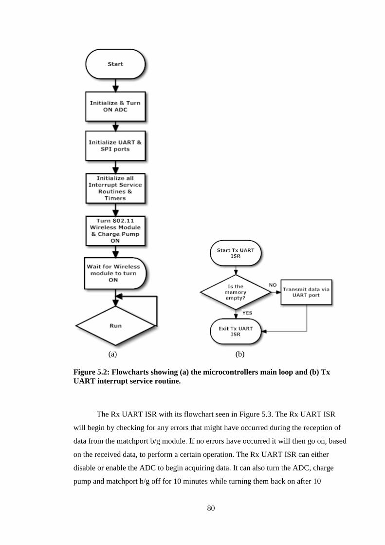
80
(a) (b)
Figure 5.2: Flowcharts showing (a) the microcontrollers main loop and (b) Tx
UART interrupt service routine.
The Rx UART ISR with its flowchart seen in Figure 5.3. The Rx UART ISR
will begin by checking for any errors that might have occurred during the reception of
data from the matchport b/g module. If no errors have occurred it will then go on, based
on the received data, to perform a certain operation. The Rx UART ISR can either
disable or enable the ADC to begin acquiring data. It can also turn the ADC, charge
pump and matchport b/g off for 10 minutes while turning them back on after 10

81
minutes. The Rx UART ISR can also turn the ADC, charge pump and matchport b/g off
for 1 minute, while turning them back on after 1 minute.
Figure 5.3: Flowchart showing the microcontrollers Rx UART interrupt service
routine.

82
The falling edge of the CNVST will trigger the ADC conversion process to
begin. This operation on the CNVST has to be periodically triggered at the necessary
sampling rate. The flowchart of Timer 3, shown in Figure 5.4 (a), was used to trigger
the ADC to sample data every 12.5µs (corresponding to a frequency of 80kHz).
Timer 7 was used to turn the matchport b/g module, ADC and charge pumps on
and off. The matchport b/g module was turned on and off by setting the gate pin of the
MOSFET to a high or low state, as discussed in section 4.3.5. The charge pumps were
turned on and off by setting the SHDN pin high or low as discussed in section 4.3.5.
The ADC was shut down by setting the SS2-Chip Select pin low. Figure 5.4 (b) shows
the simple flowchart for the Timer 7 ISR.
(a) (b)
Figure 5.4: Flowcharts showing (a) the microcontrollers TIMER 3 ISR and (b)
TIMER 7 ISR.
The INT1 ISR is triggered when the ADC‟s BUSY pin, as seen in Figure 4.3,
goes low. The ADC uses its BUSY pin to inform the microcontroller that an analog-to-
digital conversion has finished and that the digital data is ready to be read. The
flowchart of the INT1 ISR can be seen in Figure 5.5. Once the newly acquired ADC
data has been read via the SPI port, the ISR will wait until 4 data points have been
collected. When this takes place a four point moving average will be executed on both
channels and the average values will be stored in the microcontroller‟s onboard
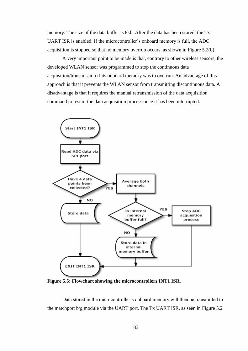
83
memory. The size of the data buffer is 8kb. After the data has been stored, the Tx
UART ISR is enabled. If the microcontroller‟s onboard memory is full, the ADC
acquisition is stopped so that no memory overrun occurs, as shown in Figure 5.2(b).
A very important point to be made is that, contrary to other wireless sensors, the
developed WLAN sensor was programmed to stop the continuous data
acquisition/transmission if its onboard memory was to overrun. An advantage of this
approach is that it prevents the WLAN sensor from transmitting discontinuous data. A
disadvantage is that it requires the manual retransmission of the data acquisition
command to restart the data acquisition process once it has been interrupted.
Figure 5.5: Flowchart showing the microcontrollers INT1 ISR.
Data stored in the microcontroller‟s onboard memory will then be transmitted to
the matchport b/g module via the UART port. The Tx UART ISR, as seen in Figure 5.2

84
(b), will check if data is available for transmission and will then transmit 32 data bits at
a time to the matchport b/g module.
5.3 Development of the PC-based wireless receiver code
5.3.1 LabVIEW programming language
National Instrument‟s LabView is a graphical programing language for test,
measurement, and control systems. LabView has the flexibility of a programming
language with an array of available functions, for I/O operations, control, analysis, and
data presentation. Code that is normally scripted in other programming languages is
entered as graphical icons in LabVIEW. A functioning LabVIEW code is called a
virtual instrument (VI). Graphical icons are wired together to build the required users
application.
5.4 Development of the PC-based data acquisition code
5.4.1 DAQ card and wireless data acquisition and processing code
Three different sets of LabVIEW-based data acquisition and data processing
programs were developed. The high processing speed required to acquire and save data
from the DAQ card and wireless sensor did not allow the concurrent processing of that
data. Thus, the acquisition and subsequent processing of the acquired data was split.
Two separate LabVIEW programs performed the processing of the acquired data.
The data acquisition program presented in this section integrates the code
necessary to acquire data using the onboard DAQ card with the code necessary to
command and acquire data transmitted wirelessly from the wireless sensor. The second
program processes the stored data which was acquired from the DAQ card and the
wireless sensor. The third program performs a Fast Fourier Transform (FFT) on the
measured data using the DAQ card and wireless sensor waveforms.
The flowchart of the data acquisition program, shown in Figure 5.6 (a), details
the processes performed by the LabVIEW program. The program was designed to
transmit commands to the wireless sensor and based on the users chosen commands,
different processes will run. If the chosen command stops the wireless sensor from
85
acquiring data then the program terminates. If the chosen command turns the wireless
sensor OFF for one minute or 10 minutes then the program will again terminate.
However, if the chosen command starts the wireless sensors data acquisition
process, then the program will begin to expect data. The moment the command that
starts the wireless transmission of data is sent, the DAQ card will also initialize so as to
begin acquiring data. The DAQ card acquires both the applied voltage and leakage
current waveforms, at a sampling rate of 80kHz. A four-point moving average function
is applied to the acquired waveforms of the applied voltage and the leakage current,
measured with the DAQ card for anti-aliasing purposes. The subsequently filtered
20kHz DAQ card and wireless sensor data are then stored in a series of files for later
analysis. Each file contains four data columns of 1 million points each corresponding to
50 seconds worth of experimental data.
The flowchart of the data processing program, shown in Figure 5.6 (b), details
the different processing functions performed by the developed LabVIEW routine. The
general data processing programme was designed to read the stored data from the tests,
and apply a number of common functions whose results may be used to indicate
changes in the applied voltage and leakage current waveform and store the results. The
functions that were applied to both the DAQ card and wireless sensor data are Root
Mean Square (RMS) of the applied voltage and leakage current, Total Harmonic
Distortion (THD) of the applied voltage and leakage current, average power,
accumulated energy and average resistance. For calculating the absolute peak value
from the leakge current waveforms, the flowchart shown in Figure 5.6(c) was used.
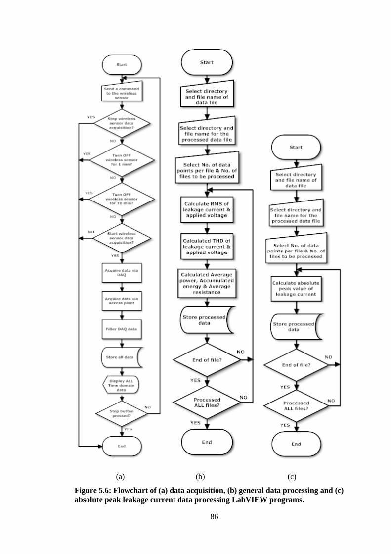
86
(a) (b) (c)
Figure 5.6: Flowchart of (a) data acquisition, (b) general data processing and (c)
absolute peak leakage current data processing LabVIEW programs.

87
The flowchart of the FFT data processing program, given in Figure 5.7, shows
the processes performed by the developed routine. The data processing program was
designed to read DAQ card and wireless sensor stored data from the tests, apply an FFT
on a single 50Hz cycle of both the applied voltage and leakage current waveforms, and
store the results.
Figure 5.7: Flowchart of FFT data processing LabVIEW program.
5.4.2 Wireless data acquisition and processing code
The flowchart for the wireless sensor only data acquisition program, can be seen
in Figure 5.8. The program was designed to transmit commands to the wireless sensor
and based on the user‟s chosen commands, different processes will run. If the chosen
command stops the wireless sensor from acquiring data then, the program terminates. If

88
the chosen command turns the wireless sensor OFF for one minute or 10 minutes, then
the program will again terminate. However, if the chosen command starts the wireless
sensors data acquisition process, then the program will begin to expect data. Data
arriving are stored on disk and displayed on the monitor, until another command is
chosen.
Both of the wireless sensor‟s input channels have a sampling rate of 20kHz and
the transmitted data is stored in a series of files for later analysis. Each file contains two
data columns of 1 million points each corresponding to 50 seconds worth of
experimental data.
The flowchart for the data processing program for files containg only wirelessly
acquired data is identical to that shown in Figure 5.6 (b). Changes to the program were
made with regards to removing the DAQ data processing capabilty, as only wirelessly
transmitted data requires processing.
The flowchart for the FFT data processing program for files containing only
wirelessly acquired data is identical to that given in Figure 5.7. While changes to the
program were made with regards to removing the FFT DAQ data processing capabilty,
the overall function of the program was unchanged.

89
Figure 5.8: Flowchart of wireless data acquisition LabVIEW program

90
5.4.3 LabVIEW functions used for data processing
The routines developed on the LabVIEWplatform to analyze the data include the
derivation of a number of parameters. The absolute peak magnitude of the leakage
current is calculated by converting all points in the array into absolute values and
searching for the maximum value. Hence, the highest absolute value over one cycle is
recorded.
The root mean square of a signal i(t) is defined as:
(4.1)
where T is the period of measurement. In the present case, its equivalent to one cycle at
50Hz. In the developed program, the RMS values for a cycle are calculated numerically
using Equations (4.2) and (4.3):
(4.2)
(4.3)
where N is the number of samples per cycle, which in the present work is 400.
The average power is calculated from the instantaneous power. The
instantaneous power is given by the product of the voltage and current at a given time:
(4.4)
The average power Pav for a cycle is then given by:
(4.5)
In the program, the instantaneous power is calculated numerically by multiplying the
voltage and current values for each sampled point, thus:

91
(4.6)
The average power is calculated by summing the values of instantaneous power and
dividing by the number of samples for the cycle, thus:
(4.7)
where N is the number of samples per cycle, which in the present work is 400.
The accumulated energy with time during the test is calculated by adding the
energy per cycle for each record to a running total. The energy is calculated from the
average power, from Equation (4.8):
(4.8)
An FFT computes the Discrete Fourier Transform (DFT) and produces exactly
the same result as evaluating the DFT definition directly; the only difference is that an
FFT is much faster. The DFT is defined by the formula:
(4.9)
where k=0,…, N-1 and N are the total number of samples, which in the present work is
400. The frequency content of the applied voltage and leakage current signal is
calculated by means of a LabVIEW library „Amplitude Spectrum VI‟. The calculated
frequency components are the amplitudes of the harmonics of the input signal. The
chosen sampling rate of N = 400 samples per cycle, allows the harmonic content of the
leakage current to be calculated up to the first 200 harmonics.
The harmonic content of the applied voltage and leakage current signal is
calculated using the THD equation:
(4.10)

92
where F denotes the amplitude of the given frequency and F1 is the fundamental
frequency.
5.5 Conclusion
Software routines were developed for the operation of the microcontroller, using
C30 programming language, within the desired limits of the condition monitoring tasks
to be carried out in this work. In addition, data acquisition and analysis routines were
developed on a LabVIEW platform to allow full exploitation of the test data transmitted
using the developed wireless sensor system.
93
Chapter 6 Laboratory and field data acquisition trials of the developed wireless sensor system: Application to polluted insulators and earth impedance measurements
6.1 Introduction
This chapter is divided into two main sections: The first section presents the
wireless measurements on two polluted insulators under artificial pollution conditions in
a laboratory fog chamber and the second section presents the wireless impedance
measurements of a 275kV transmission earth tower base field test.
The laboratory test is concerned with the measurement of the applied voltage
and leakage current waveforms of two artificially polluted porcelain insulators using the
WLAN sensor and a direct wired measurement though a DAQ card. This was done in
order to determine whether the WLAN sensor can wirelessly transmit accurately the
acquired data in a continuous manner in a high voltage laboratory environment. The
solid layer method of BS EN 60507 [119] was followed during this experiment, and two
porcelain insulators were artificially polluted and tested.
The field test is concerned with the wireless earth impedance measurement of a
purpose built 275kV transmission tower base. The 90 degree method, a variation of the
fall-of-potential was used, which is considered the most reliable method for determining
the power-frequency impedance of a substation earthing system. The field test measured
the injected current and earth potential rise voltage of the tower base, using the WLAN
sensor only, in order to measure the earth impedance of two and four tower legs. The set
of tests were performed to determine the WLAN sensors measurement capability, while
at the same time assessing the performance of the WLAN Sensors in an outdoor
environment. A comparison with standard earthing measurements results was
conducted.

94
6.2 Laboratory test arrangement
6.2.1 Porcelain insulator
Two anti-fog cap and pin porcelain insulators were tested. The „healthy‟
porcelain insulator is shown in Figure 6.1(a, b, c), while the porcelain insulator which
was in a damaged (chipped) condition is shown in Figure 6.1(d,e,f). The damaged
insulator, as seen in Figure 6.1(d,e,f) has a portion of its outer edge chipped off. The
size of the chipped off porcelain is about 7.5cm in length, 1.5cm in width and 1cm in
height, measured following the longest possible paths. Both insulators were
manufactured with a creepage length of 320 mm.
a) Top view – Healthy Insulator d) Top view – Chipped Insulator
b) Bottom view – Healthy Insulator e) Bottom view – Chipped Insulator

95
c) Side view – Healthy Insulator f) Side view – Chipped Insulator
Figure 6.1: Healthy and damaged porcelain test insulators.
6.2.2 Fog Chamber
The tests were performed in a fog chamber facility as shown in Figure 6.2. The
chamber was located within a lockable earthed high voltage test cage. The material of
the chamber was polypropylene and the chamber has a volume of 12 m3. The insulator
under test can be viewed through the door of the chamber which was made from
transparent polycarbonate.
The test insulator was attached to a tubular aluminium conductor passing
through the roof of the chamber, which allowed the test voltage to be applied to the
insulator. To reduce corona discharges, stress control rings were located at positions
along the conductor, as shown in Figure 6.2. The floor of the chamber was covered with
an earthed mesh.
'Air-atomising' spray nozzles conforming to BS EN 60507 requirements were
used to generate the fog. In order to produce a uniform fog distribution around the test
insulator, the nozzles were positioned accordingly. A pair of nozzles was positioned on
the floor, while two pairs were positioned in opposite corners of the chamber. The water
used to perform the fog chamber test was collected and pumped into the sewage system.

96
Figure 6.2: Fog chamber test arrangement for polluted insulator
1: High-voltage source, 2: Mixed resistive-capacitive HV divider, 3: Variable
resistance box, 4: High-voltage conductor, 5: Corona shield, 6: Fog chamber, 7:
Spray nozzle, 8: Test object, 9: Leakage current output, 10: Earthing mesh, 11:
HV divider output, 12:Surge protection box, 13: WLAN sensor, 14: Fog/rain
control unit 15: WLAN Access point, 16: Surge protection and low pass filter, 17:
PC containing DAQ card.
The testing of the insulators under controlled conditions of wetting was
performed though the use of a control unit located outside the high voltage compound,
that could vary the fog flow rate, air pressure and number of active fog spray nozzles.
6.2.3 Test circuit
The test circuit is shown in Figure 6.3. The test voltage was supplied by a 760 V to
75 kV, 150 kVA test transformer set. The Hipotronics AC Dielectric Test Sets adopted
for the fog chamber tests consists of the following elements:

97
a) PLC Control unit (Model CAC-PLC-4)
b) Regulation unit (Model Vrac-150-L-K)
b.1) HV ON/OFF contactor
b.2) Peschel variable transformer
c) HV test transformer (Model HHT775-150-25967)
d) Mixed Resistive-Capacitor divider (RCR-150)
e) Capacitance ( Haefely 1000pF, 200kV)
f) Resistor divider (R1 and R2, each of 33M)
g) Test object
Figure 6.3: High voltage test circuit.
The mixed resistive-capacitive divider has a ratio of 3850 to 1. The test
transformer and divider were located within the high-voltage test cage, adjacent to the
fog chamber. The porcelain insulators leakage current waveform was acquired using a
variable resistance connected in series with the test insulator and earth. The variable
resistance box consists of a decade resistance box, shown in Figure 6.2 (#3), allowing
for a large range of leakage currents to be measured. The resistance values were
adjusted manually, according to the expected level of leakage current.
6.2.4 Data Acquisition Card
A Data Acquisition (DAQ) card is used in conjunction with the wireless sensor,
as seen in Figure 6.2 and its specifications are presented in this section. The DAQ card
is an analogue to digital converter (ADC) coupled with an interface that allows a
personal computer to control the actions of the ADC, and at the final stage provide the
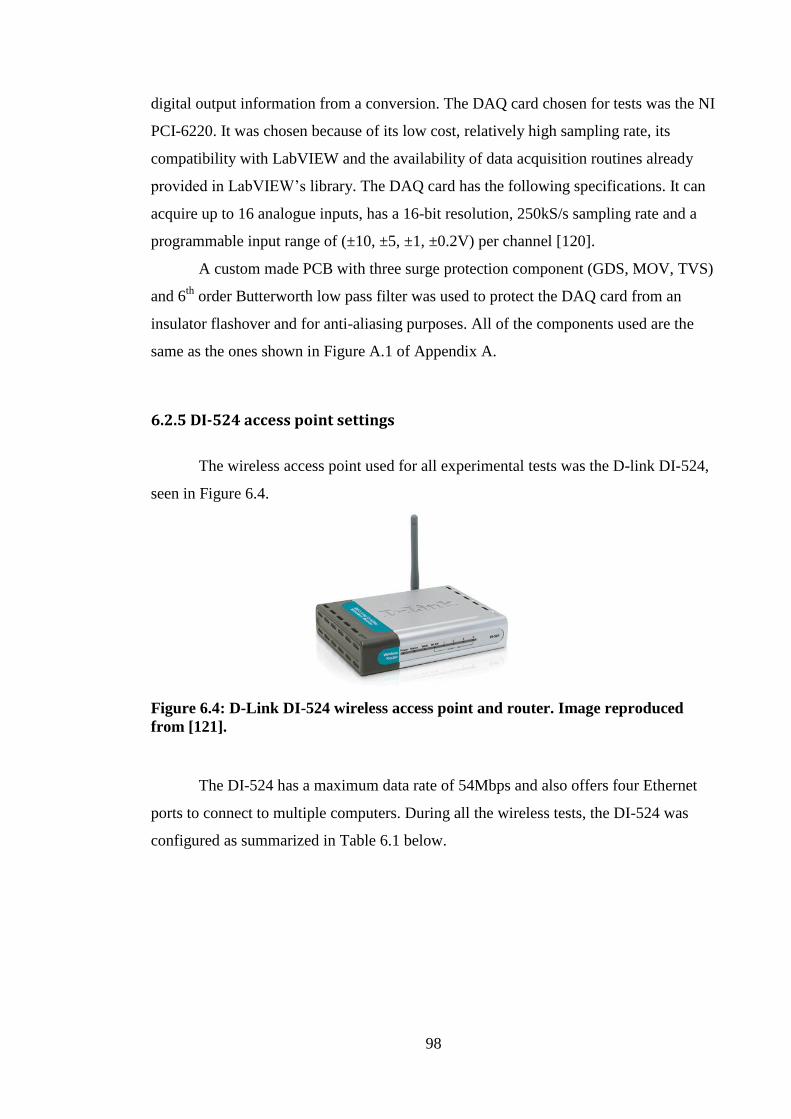
98
digital output information from a conversion. The DAQ card chosen for tests was the NI
PCI-6220. It was chosen because of its low cost, relatively high sampling rate, its
compatibility with LabVIEW and the availability of data acquisition routines already
provided in LabVIEW‟s library. The DAQ card has the following specifications. It can
acquire up to 16 analogue inputs, has a 16-bit resolution, 250kS/s sampling rate and a
programmable input range of (±10, ±5, ±1, ±0.2V) per channel [120].
A custom made PCB with three surge protection component (GDS, MOV, TVS)
and 6th
order Butterworth low pass filter was used to protect the DAQ card from an
insulator flashover and for anti-aliasing purposes. All of the components used are the
same as the ones shown in Figure A.1 of Appendix A.
6.2.5 DI-524 access point settings
The wireless access point used for all experimental tests was the D-link DI-524,
seen in Figure 6.4.
Figure 6.4: D-Link DI-524 wireless access point and router. Image reproduced
from [121].
The DI-524 has a maximum data rate of 54Mbps and also offers four Ethernet
ports to connect to multiple computers. During all the wireless tests, the DI-524 was
configured as summarized in Table 6.1 below.

99
Table 6.1: DI-524 firmware settings for the all tests.
DI-524 Firmware Options Value Comments
Wireless Enabled
Network SSID WLAN_Sensor_Ntwrk
Channel 1,6,11 Channels used
during testing
Security WPA2 - AES Pre-shared key
(PSK)
MTU 1500 default
Beacons Interval 100 Milliseconds
(default)
RTS Threshold 2432 default
Fragmentation 2346 default
DTIM Interval 3 default
Wireless Mode Mixed mode
Tx Rates Auto
SSID Broadcast Enabled
Firmware version V2.06
6.3.4 Laboratory test procedure
The solid layer test procedure method from BS EN 60507 was used. Before each
test, the insulators were carefully cleaned using warm water so as to remove any traces
of dirt, grease or any other contamination. When large continuous wet areas were
observed, the insulators surface was considered sufficiently clean.
6.3.4.1 Composition of the contaminating suspension
The contaminating suspension was prepared according to the Kaolin
composition of BS EN 60507. A „medium‟ pollution, according to BS EN 60507 was
chosen for both tests, corresponding to a volume conductivity of 3 Sm-1
at a temperature
of 20 °C. To achieve this volume conductivity, 10 g of Kaolin, 1000 g of tap water, 0.5
g of wetting agent (Triton X-l00) and a suitable amount of salt (sodium chloride) were
used. A volume conductivity of 3 Sm-1
at a temperature of 20 °C was measured, using a
Hanna Instruments Ltd. volume conductivity portable meter (model no.: HI8733) . The
volume conductivity was measured using the conductivity meter and corrected for
temperature, where necessary, using the following formula from BS EN 60507:

100
K20 = Kθ*(l-b(θ-20))
Where:
θ is the temperature of the insulator surface (°C)
Kθ is the layer conductivity at temperature of θ °C (uS)
K20 is the layer conductivity at a temperature of 20°C (uS)
b is a factor depending on temperature. The value of b as a function of temperature is
given in Table 1 of BS EN 60507.
6.3.4.2 Application of the pollution layer
The suspension, having a volume conductivity of 3 Sm-1
, was poured over the
previously cleaned and dry insulators. The pollution layer was allowed to dry naturally
for a minimum of eight hours.
6.3.4.3 High-voltage test procedure
Two pollution tests using applied high voltage levels were performed. To study
the effects on the leakage current under a „medium‟ pollution level, at the same test
voltage, for healthy and degraded insulator. The test was designed to replicate the
voltage and leakage current waveforms for the polluted and wetted insulators under
conditions approximating those experienced in-service.
The fog generation was started and maintained at a constant steady rate of flow,
of 3.5 L/hr and nozzle air pressure of 2.75 bar. The water flow rate and nozzle air
pressure chosen was based on previous measurements for the same type of insulator
[122]. With the chosen values, the maximum layer conductance would reach its
maximum value within 20 minutes. The test voltage of 11 kV used for the experiments
coincides with the highest voltage that the insulator is required to withstand under
normal operating conditions.
For both tests the insulator was installed in the chamber and energized at 820V,
while the fog generation was started and maintained for 20 minutes. After 20 minutes
had passed, the test voltage was increased to 11 kVrms and the voltage and leakage
current were recorded continuously for a 10 minute period.

101
The BS EN 60507 artificial pollution test requires the energized insulator to a 1
hour exposure of clean fog. The energized insulators exposure to clean fog for 10
minutes, was used to obtain sufficient continuous data and allow acquisition of various
V and I waveshapes using the developed wireless sensor system.
6.4 Test results
6.4.1 Porcelain insulator test
Figure 6.5 shows the leakage current waveforms of the polluted healthy
insulator measured using the WLAN sensor and DAQ card at the very beginning of the
10 minute test. A significant delay can be observed between the two waveforms, with
the leakage current waveform measured using the DAQ card leading that of the WLAN
sensor. This delay was an expected problem and was calculated from the data files to be
21.8 ms. The delay is attributed to the fact that any wireless transmission takes time to
reach its recipient, its digital content is checked for errors and finally the transmission is
acknowledge by the recipient as successful, before the transmitted data is considered
valid.
Figure 6.5: Leakage Current waveforms of healthy polluted insulator.
Delay of 21.8ms DAQ Card WLAN Sensor
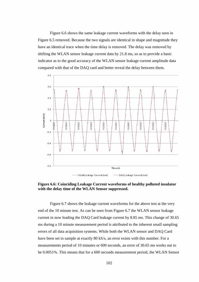
102
Figure 6.6 shows the same leakage current waveforms with the delay seen in
Figure 6.5 removed. Because the two signals are identical in shape and magnitude they
have an identical trace when the time delay is removed. The delay was removed by
shifting the WLAN sensor leakage current data by 21.8 ms, so as to provide a basic
indicator as to the good accuracy of the WLAN sensor leakage current amplitude data
compared with that of the DAQ card and better reveal the delay between them.
Figure 6.6: Coinciding Leakage Current waveforms of healthy polluted insulator
with the delay time of the WLAN Sensor suppressed.
Figure 6.7 shows the leakage current waveforms for the above test at the very
end of the 10 minute test. As can be seen from Figure 6.7 the WLAN sensor leakage
current in now leading the DAQ Card leakage current by 8.85 ms. This change of 30.65
ms during a 10 minute measurement period is attributed to the inherent small sampling
errors of all data acquisition systems. While both the WLAN sensor and DAQ Card
have been set to sample at exactly 80 kS/s, an error exists with this number. For a
measurements period of 10 minutes or 600 seconds, an error of 30.65 ms works out to
be 0.0051%. This means that for a 600 seconds measurement period, the WLAN Sensor
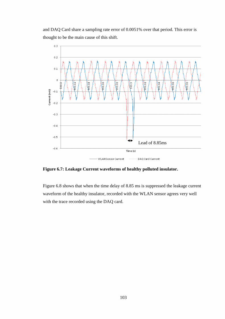
103
and DAQ Card share a sampling rate error of 0.0051% over that period. This error is
thought to be the main cause of this shift.
Figure 6.7: Leakage Current waveforms of healthy polluted insulator.
Figure 6.8 shows that when the time delay of 8.85 ms is suppressed the leakage current
waveform of the healthy insulator, recorded with the WLAN sensor agrees very well
with the trace recorded using the DAQ card.
Lead of 8.85ms

104
Figure 6.8: Coinciding Leakage Current waveforms of healthy polluted insulator,
with the lead time of the WLAN Sensor suppressed.
Results for the healthy polluted insulator show a leakage current starting off as a
distorted sinewave, as shown in Figure 6.9, with its corresponding FFT in Figure 6.10.
Figure 6.9 shows the current waveform with two distinctive peaks. The waveform is
also largely symmetrical along its x-axis. The FFT of the leakage current shows small
3rd
, 5th
, 11th
and 17th
fundamental components which further indicates a distorted
sinewave. The operating voltage harmonic content remains relatively constant
throughout the 10 minute test, which is further supported with the voltage THD shown
in Figure 6.16(e). The THD of the operating voltage remains constant at around 2.2%
throughout the experiment. A typical operating voltage FFT can be seen in Figure 6.11,
and is largely described by its 50 Hz fundamental frequency with two very small 5th
and
11th
harmonic components. It should be noted that Figure 6.11 shows the operating
voltage‟s harmonic content of up its 20th
harmonic. This was performed as the
magnitude of its harmonic content above the 20th
harmonic is low.

105
Figure 6.9: Operating voltage and leakage current of a healthy polluted insulator.
Figure 6.10: FFT of leakage current showing a frequency window of 0-1000Hz.
Figure 6.11: FFT of operating voltage showing a frequency window of 0-1000Hz.

106
Figure 6.12: Operating voltage and leakage current of a healthy polluted insulator
with surface discharges.
As the fog chamber test progresses small magnitude surface discharges begin to
occur. Two typical, peaks in magnitude attributed to surface dryband discharges can be
seen in Figure 6.12 and Figure 6.13. Both leakage current waveforms are described by a
sharp rise in magnitude at the peaks and minor distortion of operating voltage, which
are essential due to regulation in the voltage source. The distorted leakage current
waveforms seen in Figure 6.12 and Figure 6.13 now resemble positive and negative
pulses about the x-axis, rather than sinewaves. A very large 3rd
harmonic component,
now close to 30-40% of the fundamental is evident, as well as relatively large 5th
, 7th
,
9th
, 11th
, 13th
, 15th
17th
and 19th
harmonic components, in the FFTs of the leakage
currents, which can be seen in Figure 6.14 and Figure 6.15. It should be noted that
Figure 6.14 and Figure 6.15 show the leakage current‟s harmonic content of up its 20th
harmonic. This was performed as the magnitude of its harmonic content above the 20th
harmonic is low.
Dryband discharge

107
Figure 6.13: Operating voltage and leakage current of a healthy polluted insulator
with surface discharges.
Figure 6.14: FFT of leakage current showing a frequency window of 0-1000Hz..
Figure 6.15: FFT of leakage current showing a frequency window of 0-1000Hz..
Dryband discharge

108
As the test progresses, the peak and RMS levels of the leakage current drop
further and the surface discharges become more sporadic. This is evident by the Peak,
RMS and THD of the leakage current presented in Figure 6.16(a, b, d). By the end of
the 10-minute test, the minimum RMS leakage current value has dropped from 350μA
to 100μA. The accumulated energy, shown in Figure 6.16(g), also shows a significant
reduction in its rate of change during the test, which when viewed alongside the Peak,
RMS and THD leakage current waveforms, indicate a decreasing trend in surface
current activity starting around 5 minutes into the test. This is possibly due to pollution
being washed off the insulator surface.
It should be noted that during the healthy polluted insulator 10 minute test, both the
WLAN Sensor and DAQ Card waveforms were plotted alongside each other. Time
domain waveforms of the leakage current and operating voltage of Figure 6.9, Figure
6.12 and Figure 6.13 agree well with each other. Their corresponding FFTs seen in
Figure 6.10, Figure 6.11, Figure 6.14 and Figure 6.15 also match up well.

109
a) Leakage current peak value b) RMS of leakage current
c) RMS of applied voltage d) THD of leakage current
e) THD of applied voltage f) Average power
g) Accumulated Energy
Figure 6.16: Operating voltage and leakage current characteristics for a healthy
polluted insulator measured using the WLAN sensor.
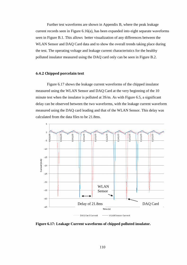
110
Further test waveforms are shown in Appendix B, where the peak leakage
current records seen in Figure 6.16(a), has been expanded into eight separate waveforms
seen in Figure B.1. This allows better visualization of any differences between the
WLAN Sensor and DAQ Card data and to show the overall trends taking place during
the test. The operating voltage and leakage current characteristics for the healthy
polluted insulator measured using the DAQ card only can be seen in Figure B.2.
6.4.2 Chipped porcelain test
Figure 6.17 shows the leakage current waveforms of the chipped insulator
measured using the WLAN Sensor and DAQ Card at the very beginning of the 10
minute test when the insulator is polluted at 3S/m. As with Figure 6.5, a significant
delay can be observed between the two waveforms, with the leakage current waveform
measured using the DAQ card leading and that of the WLAN Sensor. This delay was
calculated from the data files to be 21.8ms.
Figure 6.17: Leakage Current waveforms of chipped polluted insulator.
Delay of 21.8ms DAQ Card
WLAN
Sensor

111
Figure 6.18 also shows the leakage current waveforms of the healthy insulator,
measured using the WLAN Sensor and DAQ Card, at the very beginning of the 10
minute test when the time delay is suppressed. Figure 6.18 differs from Figure 6.17, as
the delay was removed by shifting the WLAN Sensor leakage current data by 21.8ms,
so as to provide a basic indicator as to the good accuracy of the WLAN Sensor leakage
current data compared to that of the DAQ Card and better reveal the delay between
them.
Figure 6.18: Leakage Current waveforms of chipped polluted insulator with the
delay time of the WLAN Sensor suppressed.
Figure 6.19 shows the leakage current waveforms of the chipped insulator,
polluted at 3S/m, measured using the WLAN Sensor and DAQ Card, at the very end of
the 10 minute test. As can be observed in Figure 6.19 the WLAN Sensor leakage current
in now leading the DAQ Card leakage current by 8.85ms. This change of 30.65ms
during a 10 minute measurement period is attributed to the inherent small sampling
errors of all data acquisition systems. Thus, the same sampling error rate was observed
for both the healthy and damaged polluted insulator tests.

112
Figure 6.19: Leakage Current waveforms of chipped polluted insulator.
Figure 6.20 shows the leakage current waveforms of the healthy insulator,
polluted at 3S/m, with the WLAN Sensor leakage current now shifted by 8.85ms. As
with Figure 6.18, Figure 6.20 shows a good agreement between the WLAN Sensor
leakage current data, compared to that of the DAQ Card.
Lead of 8.85ms
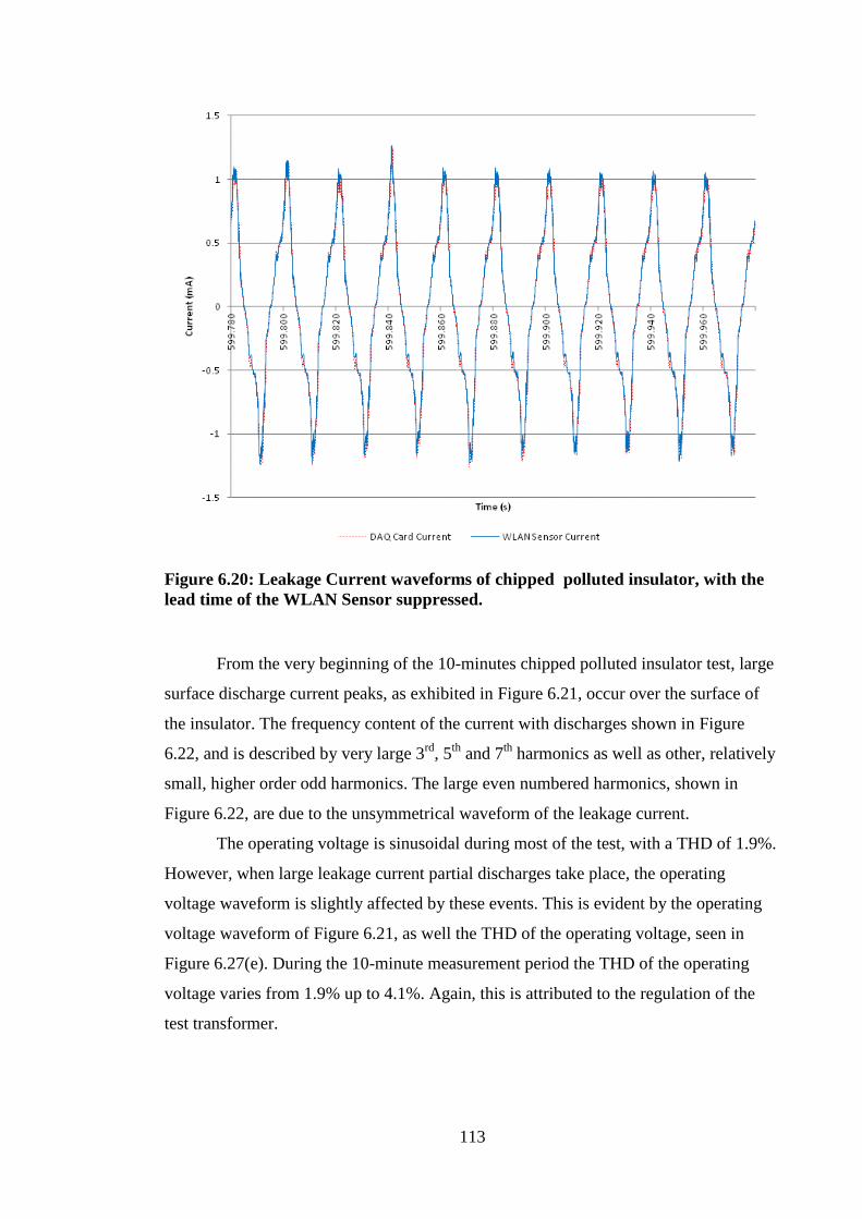
113
Figure 6.20: Leakage Current waveforms of chipped polluted insulator, with the
lead time of the WLAN Sensor suppressed.
From the very beginning of the 10-minutes chipped polluted insulator test, large
surface discharge current peaks, as exhibited in Figure 6.21, occur over the surface of
the insulator. The frequency content of the current with discharges shown in Figure
6.22, and is described by very large 3rd
, 5th
and 7th
harmonics as well as other, relatively
small, higher order odd harmonics. The large even numbered harmonics, shown in
Figure 6.22, are due to the unsymmetrical waveform of the leakage current.
The operating voltage is sinusoidal during most of the test, with a THD of 1.9%.
However, when large leakage current partial discharges take place, the operating
voltage waveform is slightly affected by these events. This is evident by the operating
voltage waveform of Figure 6.21, as well the THD of the operating voltage, seen in
Figure 6.27(e). During the 10-minute measurement period the THD of the operating
voltage varies from 1.9% up to 4.1%. Again, this is attributed to the regulation of the
test transformer.

114
Figure 6.21: Operating voltage and leakage current of a chipped polluted
insulator.
Figure 6.22: FFT of leakage current showing a frequency window of 0-1000Hz.
Figure 6.23: FFT of operating voltage showing a frequency window of 0-1000Hz.
Dryband discharge
Voltage dip due to
transformer voltage
regulation

115
Figure 6.24 shows a typical leakage current and operating voltage waveform seen 5
minutes into the polluted chipped insulator test. The leakage current waveforms is a
distorted sinewave with small 3rd
, 5th
, 11th
and 17th
frequency components as seen in
Figure 6.25. The operating voltage is largely sinusoidal as can be seen by its FFT in
Figure 6.26.
Figure 6.24: Operating voltage and leakage current of a chipped polluted
insulator.
Figure 6.25: FFT of leakage current showing a frequency window of 0-1000Hz.

116
Figure 6.26: FFT of operating voltage showing a frequency window of 0-1000Hz.
As the chipped polluted insulator test progressed surface discharges continue to
take place, as shown in Figure 6.27(a, b). With the healthy insulator, a distinct reduction
in peak and RMS leakage current values could be seen between the beginning of the test
and 5 minutes into it. This is not the case with the chipped polluted insulator. Partial
discharges with large peak values continue to occur frequently, while the typical peak
leakage current value has remained constant compared to the beginning of the test at
around 0.7mA peak.
As the test progressed the surface discharges became more sporadic. This can be
seen in the peak, RMS and THD of the leakage current waveforms, as well as the
Average power waveform, seen in Figure 6.27(a, b, d, f). While the surface discharges
became more sporadic, the typical peak value of the base leakage current remains
constant at around 0.6mA.
The resultant waveforms shown in Figure 6.21 of the polluted chipped insulator,
differ largely compared to those of the polluted healthy insulator of Figure 6.12. Surface
discharges that occur on the surface of the chipped insulator result in current peak
values that are up to 100 times larger, when compared with those of the healthy
insulator. Though a small decreasing trend of partial discharges can be seen from the
peak, RMS and THD waveforms of the leakage current in Figure 6.27(a, b, d), the
chipped insulator appears to conduct more due to the effect of the surface damage.

117
a) Leakage current peak value b) RMS of leakage current
c) RMS of applied voltage d) THD of leakage current
e) THD of applied voltage f) Average power
g) Accumulated energy
Figure 6.27: Operating voltage and leakage current characteristics for a chipped
polluted insulator measured using the WLAN sensor.

118
The Average Power and Accumulated Energy waveforms also indicate a steady
and sustained surface activity. The chipped insulators Average Power waveform has
peak values reaching 177W. These values do not compare well with the healthy
insulator ones. The Accumulated Energy waveform shows a steady increasing trend
with the chipped insulators waveform having a final value of 248kJ, while the healthy
insulators waveform had a value of 52kJ only.
It should be noted that during the polluted chipped insulator 10-minute test, both the
WLAN Sensor and DAQ Card waveforms were plotted overlying each other. Time
domain waveforms of the leakage current and operating voltage of Figure 6.21 and
Figure 6.24 agree well with each other. Their corresponding FFTs, seen in Figure 6.22,
Figure 6.23, Figure 6.25 and Figure 6.26 also match up well.
Appendix B presents the peak leakage current records as shown in Figure
6.27(a) but expanded into eight separate waveforms (see in Figure B.3). This was done
in order to visualize any differences between the WLAN Sensor and DAQ Card data
better and to better show the overall trends taking place during the test. The operating
voltage and leakage current characteristics for the healthy polluted insulator measured
using the DAQ card only can be seen in Figure B.4.
6.4.3 Analysis of results
The performance of a healthy and a damaged insulator, both artificially polluted
to the same severity, have been studied. While the main aim of this set of tests was to
understand the measuring performance of the WLAN Sensor compared to a wired data
acquisition system, some clear characteristics of the two insulators performances were
observed. The leakage current peak amplitude of the healthy insulator is fifty time less,
that of the damaged one. The average power dissipated across the healthy insulator
starts at 4W with a clear decreasing trend down to around 1W. In contrast the average
power of the damaged insulator, starts off and remains at around 5W throughout the
test, with very large peaks, of up to 177W occurring regularly. Finally, the accumulated
energy waveform of the healthy insulator shows a clear decreasing rate of change,
during the 10-minute test. This is largely contrasted by the accumulated energy
waveform of the damaged insulator, whose rate of change is relatively constant

119
throughout the test and whose final value, at 248kJ, is five times that of healthy
insulator.
While the leakage current characteristics fluctuate continuously throughout both
tests, indicating constant variations in the amplitude and waveshape of the leakage
current, the analysis performed in this work demonstrated the significant differences
between the performance of the healthy and damaged insulators.
6.5 Wireless impedance measurement field test
6.5.1 Impedance measurement system
It is recommended in the IEEE standard 81.2 [36] that the impedance of an
earthing system is measured using AC injection. Previous work on earthing systems at
Cardiff University has led to the successful development of an Impedance Measurement
System referred to as IMS [37]. Figure 6.28 shows the circuit configuration used for the
IMS system with the WLAN Sensor connected. The main components of this system,
shown in Figure 6.29, are 2 Perkin Elmer 7225 lock-in amplifiers [123] and a QSC
PLX2402 power amplifier [124].
A lock-in amplifier is a type of amplifier that can extract a signal with a known
carrier wave from an extremely noisy environment. To perform this operation a strong,
clean reference signal with the same frequency as the received signal needs to be used.
A lock-in amplifier is often used to measure phase shift, even when the signals are large
and of high signal-to-noise ratio, and do not need further improvement [123].
For the experimental setup shown in Figure 6.28 one of the Perkin Elmer 7225
lock-in amplifiers produced a high precision sinewave of adjustable frequency and
amplitude as a reference signal. This reference output signal feeds both the power
amplifier and the second lock-in amplifier. The output of the power amplifier drives the
AC current into the earthing system under test.

120
Figure 6.28: Circuit Configuration used for the IMS system and WLAN sensor.
The injected current which is generated by the power amplifier will result in a
potential difference between two chosen locations, depending on the actual
configuration of the earthing system under test. The current injected into the earthing
system under test and earth potential rise are measured using a current transformer and
differential probe. The outputs from the current transformer and differential probe are
fed into the lock-in amplifiers and the WLAN Sensor inputs to enable comparison of the
two measurement systems and assess the performance of the developed WLAN sensor
system.
Figure 6.29: Lock-in amplifiers and power amplifier of the IMS.

121
The differential probe used is the DP-25 [125], manufacture by Pintek Electronics Co.,
Ltd and shown in Figure 6.30(a). The DP-25 has a 0-25MHz bandwidth and three
selectable attenuation levels of 20, 50 and 200. The current transformer used, shown in
Figure 6.30(b), is the 58MH100 [126] manufactured by LILCO Ltd UK. The current
transformer has a 0.1 V/A sensitivity and a bandwidth of 1.5Hz to 20MHz.
a) DP-25 Differential probe b) 58MH100 Current transformer
Figure 6.30: Voltage and current transducers used for the IMS system.
6.5.2 Field test arrangement
A satellite image of the Llanrumney test site can be seen in Figure 6.31. In
Figure 6.31 the black dot (D), represents the location of the current return earth rod. The
tower footings are shown as small yellow dots, while the black dot (A) refers to the
location of the remote computer and 802.11 access point, (B) indicates the location of
the IMS and WLAN Sensor and the location of the reference voltage electrode is at
point (C).
The reinforced concrete tower legs have a depth of 3m, and the distance between
the legs at the ground surface is 7.25m. The current return electrode is a 16mm diameter
copper rod driven to a depth of 2.4m. The remote computer and access point were
placed on a wooden table at location (A). The IMS and WLAN Sensor were also placed
on a wooden table, at location (B).
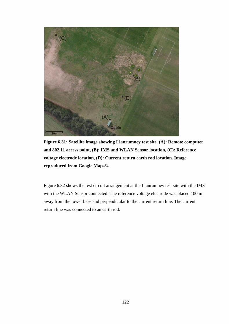
122
Figure 6.31: Satellite image showing Llanrumney test site. (A): Remote computer
and 802.11 access point, (B): IMS and WLAN Sensor location, (C): Reference
voltage electrode location, (D): Current return earth rod location. Image
reproduced from Google Maps©.
Figure 6.32 shows the test circuit arrangement at the Llanrumney test site with the IMS
with the WLAN Sensor connected. The reference voltage electrode was placed 100 m
away from the tower base and perpendicular to the current return line. The current
return line was connected to an earth rod.

123
Figure 6.32: Block diagram of IMS test at the Llanrumney test field.
A directional 10dBi antenna, shown in Figure 6.33 was connected to the DI-524 access
point via a 2 m in length low loss (LLC 200) coaxial cable and this is adopted for the
Llanrumney field test only. This was done in order to increase the signal strength due to
the larger distance between the WLAN sensor and the access point.
Figure 6.33: 10dBi Directional 2.4GHz antenna.
A 2 pole, 20A switch having on both ends 30 cm of aluminium wire length of 1 cm
diameter with ring tongue connectors. The switch was used to disconnect the tower base
legs from the IMS and WLAN sensor. All four of the tower legs are connected to a
common reference aluminium plate, whcih is insulated from ground using a wooden
pole. Each tower leg connects to this common point using three short in length 1cm
aluminium cables. A tower leg would be disconnected from this common point by

124
disconnecting the tower leg from the rest of the tower legs and connecting the switch in
series with it.
5.5.3 Test results
5.5.3.1 Disconnection of tower leg four
For the earth tower base impedance measurement test, the IMS was used to
inject current into the tower base. The Earth Potential Rise (EPR) and injected current
waveforms were measured for 10-minutes during this test using the WLAN Sensor.
Figure 6.34 shows the earth potential rise and injected current waveforms
measured using the WLAN Sensor on the complete tower base. As can be seen, both the
injected current and earth potential rise are sinusoidal in waveshape, which is further
confirmed by their corresponding FFTs, shown in Figure 6.35(a, b). The FFT of the
applied voltage shows a 50Hz fundamental and a small DC offset, while the FFT of the
injected current shows a small 3rd
harmonic component.
Figure 6.34: EPR and injected current for the tower base earth impedance
measurement.

125
a) Injected Current
b) EPR
Figure 6.35: FFTs of the EPR and injected current.
Figure 6.36 shows the EPR and injected current waveforms when tower leg four
has been disconnected and the IMS is now injecting current in tower legs one, two and
three only. As can be observed in the figure both the injected current and EPR are
sinusoidal in shape and the injected current reduced to a value of about 0.17A peak.
This is further confirmed from the injected currents FFT, seen in Figure 6.37(a). It
shows a 50Hz fundamental frequency reduced in magnitude by 50mA compared with
Figure 6.35(a), while also showing two small 3rd
and 7th
harmonic components. The
FFT of the applied voltage, seen in Figure 6.37(b) has not changed much compared with
Figure 6.35(b), with only a small increase of 0.47V in the magnitude of the 50Hz
fundamental frequency.
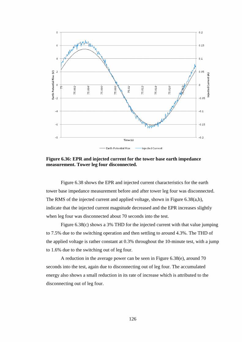
126
Figure 6.36: EPR and injected current for the tower base earth impedance
measurement. Tower leg four disconnected.
Figure 6.38 shows the EPR and injected current characteristics for the earth
tower base impedance measurement before and after tower leg four was disconnected.
The RMS of the injected current and applied voltage, shown in Figure 6.38(a,b),
indicate that the injected current magnitude decreased and the EPR increases slightly
when leg four was disconnected about 70 seconds into the test.
Figure 6.38(c) shows a 3% THD for the injected current with that value jumping
to 7.5% due to the switching operation and then settling to around 4.3%. The THD of
the applied voltage is rather constant at 0.3% throughout the 10-minute test, with a jump
to 1.6% due to the switching out of leg four.
A reduction in the average power can be seen in Figure 6.38(e), around 70
seconds into the test, again due to disconnecting out of leg four. The accumulated
energy also shows a small reduction in its rate of increase which is attributed to the
disconnecting out of leg four.

127
a) Injected Current
b) EPR
Figure 6.37: FFTs of the EPR and injected current when tower leg four was
disconnected.
Finally, the tower base impedance (
) seen in Figure 6.38(g), was
measured to be around 26 Ω, which is comparable to previous impedance measurements
for the tower base of 21 Ω [127]. When tower leg four is disconnected, the tower base
impedance settles to a new value of around 36Ω.

128
a) RMS of injected current b) RMS of EPR
c) THD of current d) THD of voltage
e) Average power f) Accumulated energy
g) Average impedance
Figure 6.38: EPR and injected current characteristics for the tower base earth
impedance measurement.
Leg 4
disconnected
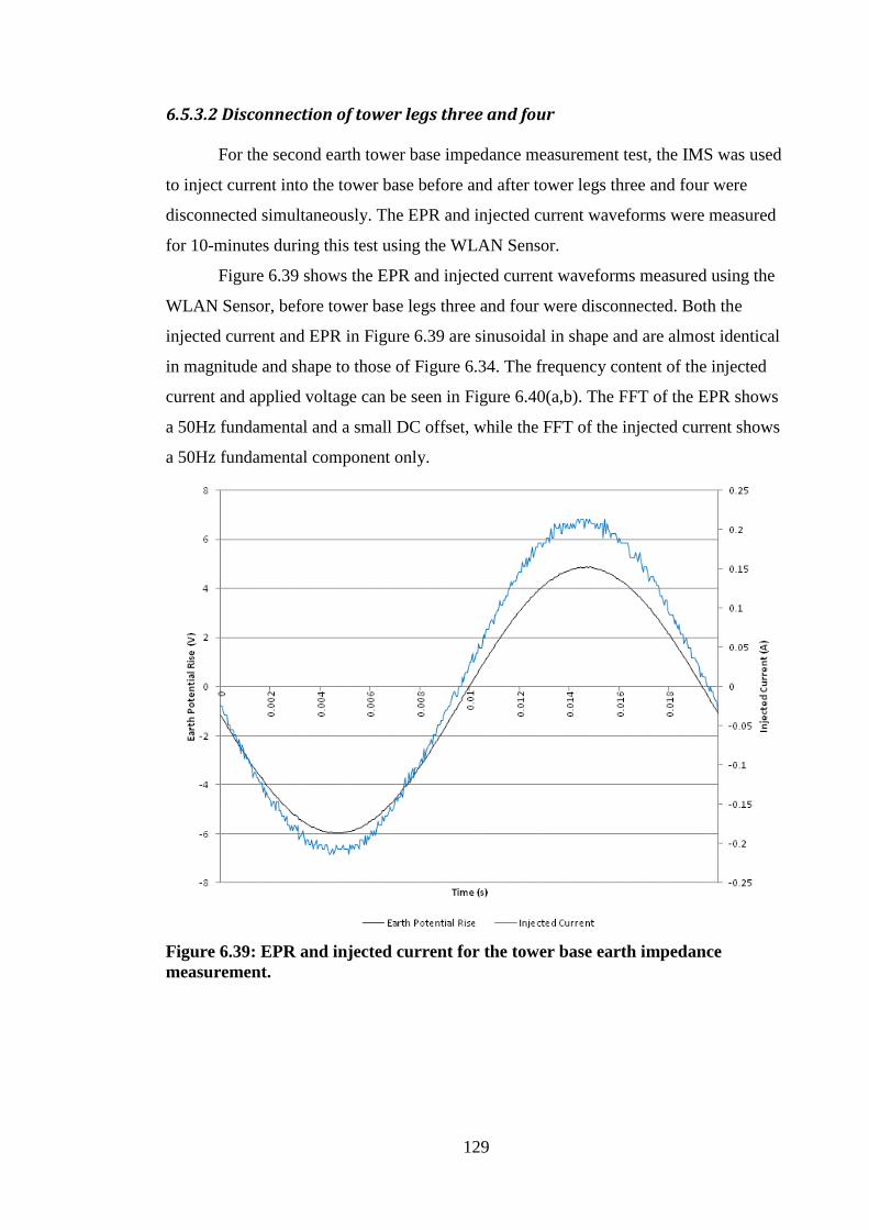
129
6.5.3.2 Disconnection of tower legs three and four
For the second earth tower base impedance measurement test, the IMS was used
to inject current into the tower base before and after tower legs three and four were
disconnected simultaneously. The EPR and injected current waveforms were measured
for 10-minutes during this test using the WLAN Sensor.
Figure 6.39 shows the EPR and injected current waveforms measured using the
WLAN Sensor, before tower base legs three and four were disconnected. Both the
injected current and EPR in Figure 6.39 are sinusoidal in shape and are almost identical
in magnitude and shape to those of Figure 6.34. The frequency content of the injected
current and applied voltage can be seen in Figure 6.40(a,b). The FFT of the EPR shows
a 50Hz fundamental and a small DC offset, while the FFT of the injected current shows
a 50Hz fundamental component only.
Figure 6.39: EPR and injected current for the tower base earth impedance
measurement.

130
a) Injected Current
b) EPR
Figure 6.40: FFTs of the EPR and injected current for the tower base earth
impedance measurement.
The measured waveforms of the applied voltage and injected current when tower
base legs three and four are disconnected can be seen in Figure 6.41. Figure 6.41 shows
that both the injected current and applied voltage are almost purely sinusoidal in shape.
By disconnecting tower base legs three and four, the injected current has reduced to
about 130mA peak. The reduction in current is further confirmed from the injected
currents FFT, shown in Figure 6.42(a), indicating a 50Hz fundamental with a magnitude
of about 130mA. The 50Hz fundamental has now reduced in magnitude to 100 mA
compared to Figure 6.40(a) while also showing a small 3rd
harmonic component. The
FFT of EPR, shown in Figure 6.42(b) has not changed significantly compared with
Figure 6.40(b), with only a small increase of 0.64V in the magnitude of the 50Hz
fundamental frequency and 60mV increase in the magnitude for the dc offset.

131
Figure 6.41: EPR and injected current for the tower base earth impedance
measurement. Tower legs three and four disconnected.
Figure 6.43 shows the EPR and injected current characteristics for the earth
tower base impedance measurement, before and after tower base leg three and four were
disconnected. The RMS of the injected current and EPR, shown in Figure 6.43(a, b),
illustrate how the injected current magnitude reduced and the EPR slightly increases,
when legs three and four were disconnected about 93 seconds into the test.
Figure 6.43(c) shows a 3.6% THD for the injected current with that value
jumping to 14% due to the switching operation and then settling to around 5.7%. The
THD of the applied voltage is rather constant at 0.3% throughout the 10-minutes test,
with a jump to 1.7% due to the disconnecting out of legs three and four.

132
a) Injected Current
b) EPR
Figure 6.42: FFTs of the EPR and injected current when tower legs three and four
were disconnected.
A reduction in the average power is seen in Figure 6.43(e), around 93 seconds
into the test, again due to disconnecting out of the two tower legs. The accumulated
energy also shows a small reduction in its rate of increase, which is again attributed to
the disconnecting out of the two tower legs. Disconnecting out of legs three and four
leads to the tower base impedance changing to a new value of around 47Ω.

133
a) Injected current b) EPR
c) THD of current d) THD of voltage
e) Average power f) Accumulated energy
g) Average impedance
Figure 6.43: EPR and injected current characteristics for the tower base earth
impedance measurement.
Leg 3+4
disconnected

134
6.5.4 Analysis of results
Both measurements of the tower base earth impedance are comparable with each
other and with previous measurements of the 275kV tower base, having an error
between them of 19%. The disconnecting of tower leg four produces a clear decrease in
the RMS value of the injected current, an increase in its THD, a decrease in the average
power, a decrease in the accumulated energy rate and increase in the impedance. While
in both tests some small fluctuation is seen throughout the tests, overall the waveforms
remained constant before and after the tower leg disconnection. This is also the case
when tower legs three and four are disconnected at the same time.
6.6 Conclusions
In this chapter, the data acquisition performance of the WLAN Sensor was
presented. The first set of tests showed the characteristics of a healthy and damaged
artificially polluted porcelain insulator, during a 10-minute artificial pollution test fog
chamber. In both tests, the WLAN Sensor data and wired DAQ card data agree well
with each other. While more tests would be beneficial, identical type insulators were
tested under the same artificial pollution test conditions, and the WLAN Sensor was
demonstrated to measure the difference in performance between the two insulators. This
indicates that the WLAN Sensor could feasibly be used to continuously monitor the
leakage currents of high voltage insulators.
In the second set of tests the earth impedance of a 275kV tower base was
measured using different combination of legs. The results presented are comparable
with previously published data for that particular tower base.

135
Chapter 7 Interference performance of the developed wireless sensor under laboratory and field test conditions
7.1 Introduction
The previous chapter presented data acquisition measurements taken using the
WLAN Sensor at the outdoor Llanrumney test field and at Cardiff University‟s high
voltage laboratory.
This chapter presents wireless performance measurements of the WLAN sensor at
the outdoor Llanrumney test field and at Cardiff University‟s high voltage laboratory,
with the intention of gaining an understanding of the sensor‟s wireless operation and
investigating any potential high voltage interference sources. The first test took place at
the outdoor Llanrumney test field, when no high voltage tests were taking place, but
within the proximity of a live 275kV transmission line. The relatively quiet outdoor test
facility allows for the „benchmarking‟ of the wireless performance of the WLAN
sensor. The wireless performance of the sensor was measured for a 10-minute
transmission period using 802.11 channels 1, 6 and 11.
The second test took place at Cardiff University‟s high voltage laboratory when
no high voltage tests were taking place. A large number of 802.11 networks were seen
using the 2.4GHz ISM spectrum. Again, the wireless performance of the sensor was
measured for a 10-minute transmission period using 802.11 channels 1, 6 and 11.
Lastly, the wireless performance of the access point and WLAN Sensor used
during the healthy and damaged polluted insulator fog chamber tests, described in
Chapter 6, is presented. This was done in order to identify whether or not wireless
interferences in the 2.4-2.5 GHz frequency range are produced during polluted insulator
fog chamber tests. The wireless performances of the three tests are then compared to
each other in order to investigate high voltage sources of interference.

136
7.2 Interference performance tests at the Llanrumney test site
7.2.1 Llanrumney field test equipment and software
The Llanrumney wireless field test consisted of commanding the WLAN Sensor
to transmit wireless measurements for 10 minutes, when no actual sources were
connected to the sensor. An Acer laptop (Intel 1.6GHz Dual Core CPU, 2GB RAM)
running the LabVIEW code described in section 5.4.2, on a Windows XP SP3 operating
system was used via a wireless command to control manually the beginning and the end
of the WLAN Sensor transmission period. The performance of the DI-524 access point
and WLAN Sensor was measured for the three non-overlapping channels 1, 6 and 11,
using the 802.11 Aipcap Tx packet capturing USB adapter [128] and the Wi-spy 2.4x
spectrum analyzer USB adapter [129], plugged into a Toshiba laptop (Intel Core 2 Duo
1.4GHz CPU, 2.85GB RAM) running Windows XP SP3 operating system. The Toshiba
laptop along with the hardware and software described above will be referred to in this
thesis as the Wi-Fi interference monitor.
Cascade Pilot PE and Excel 2007 were used for post processing and plotting of
the 802.11 packets captured using Wireshark. Appendix C contains a brief explanation
of the operation of the hardware (Airpcap Tx, Wi-spy 2.4x) and software (Wireshark,
Cascade pilot PE) as used in this chapter.
7.2.2 Llanrumney field test arrangement
The 2.4GHz industrial, scientific and medical frequency (ISM), which the
WLAN sensor uses, is license free. A very large number of 802.11 and non-802.11
device, that use this frequency spectrum for a diverse number of functions are available.
While 802.11 devices were designed to share the 2.4GHz spectrum with each other, in
practice this does not always happen optimally. Non-802.11 devices, like wireless
cameras or cordless phones in the vicinity of an 802.11 network, will generally interfere
with each other‟s wireless operation [58, 59].
The 2.4GHz spectrum measurement and concurrent 802.11 packet measurement
of a „dummy‟ WLAN sensor wireless transmission at the Llanrumney field test site
presented the opportunity to conduct a „baseline‟ measurement during a typical WLAN
Sensor transmission period. The distance between buildings and other structures from

137
the wireless field test meant that the likelihood of other 802.11 and non-802.11 devices
using the 2.4GHz spectrum in the vicinity of the WLAN sensor would be small or that
their signals would be much attenuated. Also, the relatively large distances between
structures like walls, trees or large metal objects and the WLAN sensor network
presented a more ideal environment for 802.11 devices.
The WLAN Sensor was placed at location „B‟ as indicated in Figure 7.1, and the
access point was placed at location „A‟. The distance separating the WLAN Sensor from
the access point was measured to be 60m. The WLAN sensor was placed at a height of
0.7 m, on top of a wooden platform with its antenna facing location „A‟ and in
perpendicular configuration with respect to ground surface. The Wi-Fi interference
monitor was placed at a distance of 30cm from the WLAN Sensor and perpendicular to
the imaginary line joining locations „A‟ and „B‟. The Wispy 2.4x USB adapter‟s
antenna was also perpendicular to ground surface. A 10dBi directional antenna was
placed on the roof of the cabin at location „A‟, at a height of 2.6 m and connected via a
2 m in length low loss (LLC 200) coaxial cable to the access point.
Figure 7.1: Satellite image showing Llanrumney test site. Image reproduced from
Google Maps©.

138
7.2.3 Llanrumney field test procedure
The Wi-Fi interference monitor, was placed at location „B‟, as can be seen in
Figure 7.1. Wireshark was set so as to measure the 802.11 traffic on channel 1. The
WLAN Sensor was then placed next to the laptop. A 3dBi omnidirectional „rubber
ducky‟ antenna was connected to the WLAN Sensor. The DI-524 access point was
connected to the directional gain antenna and the antenna was manually moved so as to
face the location of the WLAN Sensor. The Acer laptop, running LabVIEW, was
connected to the DI-524 access point via its Ethernet port. The Llanrumney test site
equipment configuration can be seen in Figure 7.2. The received signal strength
indicator (RSSI) value shown in Chanalyzer Pro was then used to adjust manually, in
small increments, the direction of the directional antenna so as to get the best possible
signal strength at the WLAN Sensor location.
Figure 7.2: Llanrumney test site equipment configuration
1: Acer Laptop, 2: DI-524 access point, 3: High gain directional antenna, 4: WLAN
Sensor, 5: Toshiba laptop, 6: Wi-spy2.4x spectrum analyzer, 7: AirPcap Tx packet
analyzer
Once the best possible signal strength was achieved, the Chanalyzer Pro and
Wireshark programs running on the Toshiba laptop were executed. The LabVIEW
program was then used to trigger the WLAN Sensor to begin transmitting data. After a
10 minute transmission period, the WLAN sensor was commanded to stop transmitting.
139
The Chanalyzer Pro spectrum and Wireshark 802.11 packet measurements were then
saved to file.
The DI-524 was then commanded to switch to channel 6 and the Wi-Fi
interference monitor software were once again executed. The LabVIEW program was
used to trigger the WLAN Sensor to begin transmitting data. After a 10-minute
transmission period, the WLAN sensor was commanded to stop transmitting. The Wi-Fi
interference monitor files were saved to disk.
The same process was followed for channel 11. The DI-524 was commanded to
switch to channel 11 and so was Wireshark. At the end of the transmission period the
Wi-Fi interference monitor files were saved to disk.
7.2.4 Llanrumney field test results
Throughout the Llanrumney field test, the frequency content of the 2.4GHz ISM
spectrum and the 802.11 packets were measured using the Wi-Fi interference monitor.
Figure 7.3 shows the entire „dummy‟ WLAN Sensor transmission that took
place on channel 1 at the Llanrumney test field along with two quiet periods before and
after the wireless transmission. This waterfall view, measured using the Wi-spy 2.4x
and Chanalyzer Pro, shows the amplitude over time for each frequency in the
measurement band. The colours represent power levels in the spectrum with dark blue
as low and bright red as higher amplitude levels. The mainly green and blue colored
dots scatter between channels 2410-2430MHz, represent the power levels of wireless
packets from and to the WLAN Sensor and DI-524 access point. Figure 7.3 is an
example showing that though channel 1 (center frequency of 2412MHz) is used to
transmit data, a number of other adjacent channels have their frequencies utilized. While
it is feasible to transmit data on any of the 13 channels, overlap between channels being
used at the same time may cause unacceptable degradation of signal quality and
throughput. The typical channel allocation is 1, 6 or 11, which are considered non-
overlapping channels. It should also be noted that the pattern of green, blue and red
colours shown scattered in Figure 7.3 throughout the 2.4-2.5GHz spectrum is the typical
operation of „rogue‟ access points and stations.
A number of 802.11 networks were detected during the tests and a very small
number of „PIR Security Device‟ and „ZigBee‟ non-802.11 devices were also detected
using the frequency spectrum. 802.11 and non-802.11 devices are detected
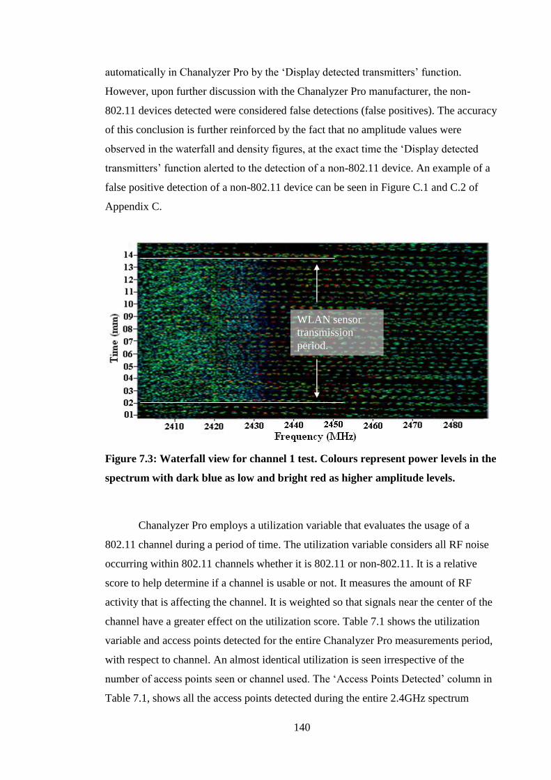
140
automatically in Chanalyzer Pro by the „Display detected transmitters‟ function.
However, upon further discussion with the Chanalyzer Pro manufacturer, the non-
802.11 devices detected were considered false detections (false positives). The accuracy
of this conclusion is further reinforced by the fact that no amplitude values were
observed in the waterfall and density figures, at the exact time the „Display detected
transmitters‟ function alerted to the detection of a non-802.11 device. An example of a
false positive detection of a non-802.11 device can be seen in Figure C.1 and C.2 of
Appendix C.
Figure 7.3: Waterfall view for channel 1 test. Colours represent power levels in the
spectrum with dark blue as low and bright red as higher amplitude levels.
Chanalyzer Pro employs a utilization variable that evaluates the usage of a
802.11 channel during a period of time. The utilization variable considers all RF noise
occurring within 802.11 channels whether it is 802.11 or non-802.11. It is a relative
score to help determine if a channel is usable or not. It measures the amount of RF
activity that is affecting the channel. It is weighted so that signals near the center of the
channel have a greater effect on the utilization score. Table 7.1 shows the utilization
variable and access points detected for the entire Chanalyzer Pro measurements period,
with respect to channel. An almost identical utilization is seen irrespective of the
number of access points seen or channel used. The „Access Points Detected‟ column in
Table 7.1, shows all the access points detected during the entire 2.4GHz spectrum
WLAN sensor
transmission
period.

141
measurement period, and the values shown include the DI-524 access point used during
the test. This means that at least one access point will always be detected.
Table 7.1: 802.11 channel utilization and access points detected
Channel Utilization Access Points Detected
1 2.6% 3
6 2.7% 2
11 2.6% 1
It should be noted that during both the Llanrumney field tests and the high
voltage laboratory tests, „rogue‟ access points with very weak signals were detected at
many points during the test and their signals were subsequently lost, only to reappear
later on in the test. Since access points are generally static, these „phantom‟ appearances
of access point were believed to occur due to small changes in the 2.4GHz spectrum
environment, which prevented the Toshiba laptops‟ 802.11 module from continuously
detecting them when combined with the very weak signals of these access points.
Table 7.2(a,b,c) show the total packets transmitted by „rogue‟ access points and
stations on channel 1, 6 and 11 respectively throughout AirPcap Tx measurements,
tabulated using Cascade Pilot PE. In Table 7.2(a) only one „rogue‟ access point could be
seen by the AirPcap Tx, which contrasts with the two measured using the Wi-spy
2.4GHz adapter. This is most likely due to the low gain internal antenna of the AirPcap
Tx adapter. The total number of packets transmitted by „rogue‟ access points and
stations during the test using channel 1 and 11 are largely the same. Channel 6 appears
to be more „noisy‟, showing an increase of over 50% in total packets transmitted.
The frame error rate, shown in Table 7.3 during the Channel 6 test, shows more
than double the error rate compared to that of Channel 1 and 11. The FER was
calculated with data exported from Wireshark.
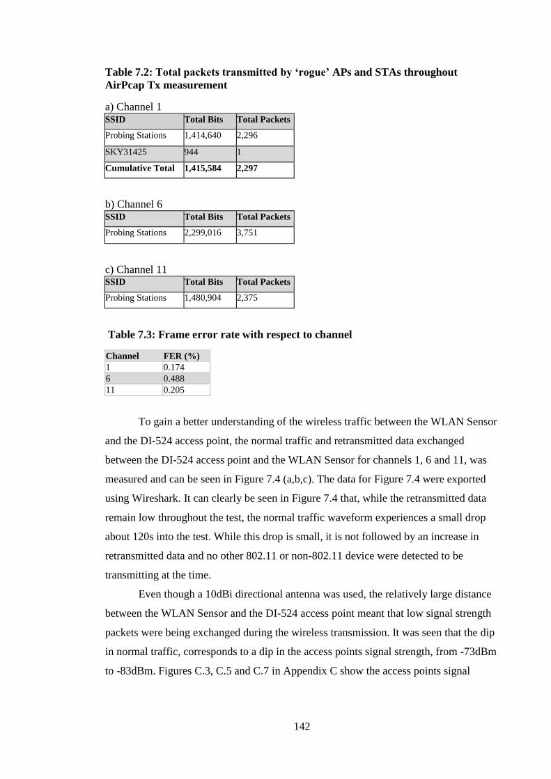
142
Table 7.2: Total packets transmitted by ‘rogue’ APs and STAs throughout
AirPcap Tx measurement
a) Channel 1 SSID Total Bits Total Packets
Probing Stations 1,414,640 2,296
SKY31425 944 1
Cumulative Total 1,415,584 2,297
b) Channel 6 SSID Total Bits Total Packets
Probing Stations 2,299,016 3,751
c) Channel 11 SSID Total Bits Total Packets
Probing Stations 1,480,904 2,375
Table 7.3: Frame error rate with respect to channel
Channel FER (%)
1 0.174
6 0.488
11 0.205
To gain a better understanding of the wireless traffic between the WLAN Sensor
and the DI-524 access point, the normal traffic and retransmitted data exchanged
between the DI-524 access point and the WLAN Sensor for channels 1, 6 and 11, was
measured and can be seen in Figure 7.4 (a,b,c). The data for Figure 7.4 were exported
using Wireshark. It can clearly be seen in Figure 7.4 that, while the retransmitted data
remain low throughout the test, the normal traffic waveform experiences a small drop
about 120s into the test. While this drop is small, it is not followed by an increase in
retransmitted data and no other 802.11 or non-802.11 device were detected to be
transmitting at the time.
Even though a 10dBi directional antenna was used, the relatively large distance
between the WLAN Sensor and the DI-524 access point meant that low signal strength
packets were being exchanged during the wireless transmission. It was seen that the dip
in normal traffic, corresponds to a dip in the access points signal strength, from -73dBm
to -83dBm. Figures C.3, C.5 and C.7 in Appendix C show the access points signal

143
strength measured at location „B‟ of Figure 7.1, using the AirPcap Tx, Wireshark and
Pilot PE software for plotting, for channels 1, 6 and 11.
The normal traffic and retransmitted data exchanged between the DI-524 access
point and the WLAN Sensor for channel 6 can be seen in Figure 7.4(b). It can be seen
that the retransmitted data experiences relatively large short increases in its value
throughout the wireless „dummy‟ transmission.
The normal traffic and retransmitted data exchanged between the DI-524 access
point and the WLAN Sensor for channel 11 can be seen in Figure 7.4(c). The normal
traffic waveform shows a relatively constant transmission rate at an average of about
720kbps and the retransmitted data is low throughout the test. The DI-524 signal
strength measured using the AirPcap Tx adapter for the channel 11 test is still relatively
low, but comparable to those of channel 1 and 6. The DI-524 signal strength for channel
11 varied from -81dBm to -76dBm throughout the test.
144
a) Channel 1
b) Channel 6
c) Channel 11
Figure 7.4: Normal traffic vs. retransmissions between DI-524 and WLAN Sensor

145
Figure 7.5(a,b,c) plotted in Cascade Pilot PE shows the amount of data that the
WLAN Sensor has transmitted at different 802.11 transmission rates. In Figure 7.5(a) a
portion of the data exchanged between the WLAN Sensor and access point has taken
place at 54, 48, 36 or even 24 Mbps. This is an indication that a higher gain antenna for
the WLAN Sensor or the access point or both, would be advantageous.
The low signal strength throughout the test during channel 1 has the negative
effect of forcing a change of the wireless networks transmission rate from 54Mbps to
lower values. This lowering of the transmission rate increases the receiver sensitivity in
both the WLAN Sensor and access point. The transmission rate adaptation mechanism
is not specified in the IEEE 802.11 standard and is left to the 802.11 access point
manufacturer to implement.
The DI-524 signal strength for the channel 6 test was relatively low and varied
from -82dBm to -75dBm throughout the test. The low signal strength, combined with
the increase in retransmitted data, is believed to have exacerbated the frequent change in
802.11 transmission rate during the „dummy‟ WLAN Sensor transmission on channel 6,
seen in Figure 7.5(b), compared to that of channel 1 shown in Figure 7.5(a).
Figure 7.5(c) shows that data transmitted from the WLAN Sensor on channel 11
mostly used the highest possible 802.11 transmission rate, of 54Mbps. This differs from
Figure 7.5(a,b) where a larger portion of the data transmitted from the WLAN Sensor
took place at transmission rates of 48Mbps, or lower.

146
a) Channel 1
b) Channel 6
c) Channel 11
Figure 7.5: Total bits transmitted with respect to transmission frame rate

147
7.3 Interference performance test in the high voltage laboratory
environment
7.3.1 High voltage laboratory test equipment and software
The high voltage laboratory wireless performance test was largely similar to that
of the Llanrumney field test. It consisted of commanding the WLAN Sensor to transmit
wireless measurements for 10 minutes when no signal sources were connected to the
sensor. A PC (Intel Pentium D 1.6GHz Dual CPU, 2GB RAM) running the LabVIEW
code described in section 5.4.2 on a Windows XP SP3 operating system was used to
control manually the beginning and the end of the WLAN Sensor transmission period
via a wireless command. The performance of the DI-524 access point and WLAN
Sensor was measured for the three non-overlapping channels 1, 6 and 11 using the Wi-
Fi interference monitor. The 2.4-2.5GHz spectrum was measured throughout the high
voltage tests using the Wi-spy 2.4x adapter along with the Chanalyzer Pro software.
Cascade Pilot PE and Excel 2007 were used for post processing and plotting of the
802.11 packets captured using Wireshark. Exactly the same firmware settings for the
DI-524 access point found in Error! Reference source not found. were used during all
three tests.
7.3.2 High voltage laboratory test arrangement
The WLAN Sensor was placed at location „B‟ as indicated Figure 7.6, and the
access point was placed at location „A‟. The distance separating the WLAN Sensor from
the access point was measured to be 2.3 m. The WLAN Sensor was placed at a height of
0.8 m, on top of a wooden table with its antenna facing location „A‟ and perpendicular
to the ground surface. The access point was placed at location „A‟ at a height of 2.3 m
from ground. A 3dBi omnidirectional „rubber ducky‟ antenna was connected to the
WLAN Sensor. The Wi-Fi interference monitor was placed at a distance of 30cm from
the WLAN Sensor, perpendicular to the imaginary line formed by locations „A‟ and „B‟.
A 3dBi omnidirectional „rubber ducky‟ antenna was connected to the DI-524 access
point.

148
Figure 7.6: High voltage laboratory floor plan. Not to scale.
The dark blue lines in Figure 7.6 represent the grounded metal mesh of the high voltage
cages and the light blue lines represent the doors of the high voltage laboratory and its
high voltage cages. The fog chamber and high voltage transformer that were used for
the artificially polluter insulator test are located inside HV Cage 2.
7.3.3 High voltage laboratory test procedure
The Wi-Fi interference monitor was placed at location „B‟, as seen in Figure
7.6. Wireshark was set up to measure the 802.11 traffic on channel 1. The WLAN
Sensor was then placed next to the laptop. A 3dBi omnidirectional „rubber ducky‟
antenna was connected to the WLAN Sensor. The DI-524 access point was placed at
location „A‟ as seen in Figure 7.6. The desktop PC, running LabVIEW, was connected
to the DI-524 access point via its Ethernet port. The received signal strength indicator
(RSSI) value shown in Chanalyzer Pro was then checked to verify that high signal
strength packets from the access point were seen at the WLAN Sensor location.
Due to the short distance separating the access point and WLAN Sensor, the
RSSI value measured was more than adequate. Once the Wi-Fi interference
monitorwas executed, the LabVIEW program running on the desktop PC was then used
to send a wireless command to the WLAN Sensor to begin transmitting data. After a 10-
minute transmission period, the WLAN sensor was commanded to stop transmitting.
The Wi-Fi interference monitor measurement files were then saved to disk..
The DI-524 was then commanded to switch to channel 6 and so was the Wi-Fi
interference monitor.. The LabVIEW program was once again used to trigger the

149
WLAN Sensor to begin transmitting data. After a 10-minute transmission period, the
WLAN sensor was commanded to stop transmitting. The Wi-Fi interference monitor
measurement files were then saved to disk. The same process was followed for channel
11.
7.3.4 High voltage laboratory interference test results
A number of 802.11 networks were detected during the high voltage laboratory
tests and a very small number of „PIR Security Device‟, „ZigBee‟ and „Wireless
Camera-PAL‟ non-802.11 devices were also detected using the frequency spectrum. As
no amplitude values were observed in the waterfall and density figures at the exact time
the „Display detected transmitters‟ function alerted to the detection of a non-802.11
device, they were considered false detections.
Table 7.4 shows the utilization variable and access points detected for the entire
Chanalyzer Pro measurements period with respect to channel. While the spectrum
measurements on channels 1 and 11 show an almost identical utilization, this cannot be
said for channel 6. The large number of access points seen on channel 6 is believed to
cause an increase in the utilization factor calculated by Chanalyzer Pro.
Table 7.4: 802.11 channel utilization and access points detected
Channel Utilization Access Points Detected
1 3.8% 10
6 4.2% 20
11 3.7% 8
Table 7.5(a,b,c) below, shows the total packets transmitted by „rogue‟ access
points and stations on channel 1,6 and 11 throughout AirPcap Tx measurement,
tabulated using Cascade Pilot PE. A near tenfold increase in the number of packets
transmitted from „rogue‟ access points and stations can be seen for channel 1 compared
with channel 1 and 11, seen in Table 7.2(a,c) during the outdoor field test.
When comparing channels 6 and 1, seen in Table 7.5(a,b), a 17% increase in the
number of packets transmitted from „rogue‟ access points and stations can be seen.
A large drop in the number of packets transmitted from „rogue‟ access points
and stations can be seen for channel 11 compared with channel 1 as seen in Table

150
7.5(c). This is largely attributed to the fewer and less active access points seen in the
vicinity of the WLAN sensor.
Table 7.5: Total packets transmitted by ‘rogue’ APs and STAs throughout
AirPcap Tx measurement
a) Channel 1 SSID Total Bits Total Packets
eduroam 13,588,960 6,325
CU-WiFi 11,086,768 6,281
CU-Guest-WiFi 11,048,832 6,087
Probing Stations 699,536 1,141
Cumulative Total 36,424,096 19,834
b) Channel 6 SSID Total Bits Total Packets
eduroam 15,462,448 7,241
CU-Guest-WiFi 13,170,792 7,407
CU-WiFi 12,811,872 7,323
Probing Stations 1,128,248 1,876
Mercure Holland House
100,056 111
Cumulative Total 42,673,416 23,958
c) Channel 11 SSID Total Bits Total Packets
Probing Stations 809,088 1,374
wcb 639,456 303
CU-Guest-WiFi 134,448 74
eduroam 129,072 60
CU-WiFi 127,520 72
CIB_2 29,336 103
Cumulative Total 1,868,920 1,986
The frame error rate seen in Table 7.6 for channel 1 was 1.5%. While the FER
still remains relatively low, a comparison of the FER for channel 1 of Llanrumney field
test site shows an 8.5 magnitude increase. The large number and high activity of „rogue‟
access points and stations using channel 6 have attributed to an increase of the FER
which reaches 1.7%. On the other hand, the relatively „quite‟ channel 11 exhibited a
much lower FER of 0.33%.

151
Table 7.6: Frame error rate with respect to channel
Channel FER (%)
1 1.476
6 1.738
11 0.330
Figure 7.7(a,b,c) shows the normal traffic and retransmitted data exchanged
between the DI-524 access point and the WLAN Sensor. It can be seen that the
retransmitted data waveform has more pronounced spikes compared to those of Figure
7.4(a,c). This is attributed to the large number and high activity of „rogue‟ access points
and stations.
Also, the normal traffic waveform experiences a small drop about 160s into the
measurement. While this drop is small, it is not followed by an increase in retransmitted
data and no other 802.11 or non-802.11 device were detected to be transmitting at the
time. It was seen that the small dip in normal traffic corresponds to a small dip in the
access points signal strength from -44dBm to -46dBm. Figures C.9, C.11 and C.13 of
Appendix C, show the access points signal strength measured at location „B‟ for
channels 1, 6 and 11.
The retransmitted data waveform for channel 6 shown in Figure 7.7(b) has a
number of very sharp but short spikes with the most pronounced being about 520s into
the test. These sharp spikes correspond well with a drop in the access point signal
strength from -39dBm to -46dBm.
The normal traffic waveform shown in Figure 7.7(c) experiences a small drop
about 360s into the measurement. It was seen that the small dip in normal traffic
corresponds to a small dip in the access points signal strength, from -37dBm to -44dBm.
A relatively stable retransmitted data waveform is seen during the WLAN Sensor
transmission on channel 11.

152
a) Channel 1
b) Channel 6
c) Channel 11
Figure 7.7: Normal traffic vs. retransmissions between DI-524 and WLAN Sensor
on channel 1

153
a) Channel 1
b) Channel 6
c) Channel 11
Figure 7.8: Total bits transmitted with respect to transmission frame rate

154
Figure 7.8(a,b,c) above shows that the amount of data the WLAN Sensor has
transmitted at different 802.11 transmission frame rates during channels 1,6 and 11.
Most of the data during the tests on channels 1 and 11 are transmitted at a transmission
frame rate of 54Mbps.
However, the higher wireless activity seen on channel 6, due to „rogue‟ access
points and stations forces, forces the exchange of data between the WLAN sensor and
the DI-524 access point to take place at slower transmission frame rates.
7.4 High voltage laboratory fog chamber tests
7.4.1 High voltage laboratory test equipment and software
During the polluted insulator fog chamber tests described in Chapter 6, the
wireless performance of WLAN Sensor and DI-524 was measured. A desktop PC (Intel
Pentium D 1.6GHz Dual CPU, 2GB RAM) running the LabVIEW code described in
section 5.4.1, on a Windows XP SP3 operating system, was used to control the
beginning and the end of the WLAN Sensor transmission period manually via a wireless
command. The performance of the DI-524 access point and WLAN Sensor was
measured on channel 6 for both tests using the AirPcap Tx adapter. The same test
equipment and software was used and configured in the same manner as that described
in sections 7.3.1.
7.4.2 High voltage laboratory test arrangement
The high voltage laboratory test arrangement was that described in section 6.3.2.
The WLAN Sensor was placed at location „B‟, seen in Figure 7.1, and the access point
was placed at location „A‟. The same test arrangement as that described in 7.3.2 was
used.
7.4.3 High voltage laboratory test procedure
The same test procedure as that described in section 7.3.3 was used. Following
the procedure for characterizing artificially polluted insulators in section 6.2 and after

155
the fog had been applied for 20 minutes,, the Wi-Fi interference monitor was executed.
High voltage was then applied to the damaged polluted insulator. The LabVIEW
program running on the desktop PC was used to trigger the WLAN sensor to begin
transmitting data. After a 10-minute transmission period, the WLAN sensor was
commanded to stop transmitting. The Wi-Fi interference monitor measurement files
were then saved to disk. The damaged insulator was swapped with the healthy polluted
one. The same process, as above, was followed for channel 6.
7.4.4 High voltage laboratory test results
As with the previous „dummy‟ WLAN Sensor transmissions in the high voltage
laboratory during both the polluted insulator fog chamber tests, a number of 802.11
networks and a very small number of „PIR Security Device‟, „ZigBee‟ and „Wireless
Camera-PAL‟ non-802.11 devices were also detected using the 2.4GHz frequency
spectrum. As no amplitude values were observed in the waterfall and density figures, at
the exact time the „Display detected transmitters‟ function alerted to the detection of a
non-802.11 device, they were considered false detections.
Table 7.7 shows the utilization variable and access points detected for the entire
Chanalyzer Pro measurements period, for the two insulator tests. Both tests show a near
identical utilization value, which is also identical to the „dummy‟ WLAN Sensor
transmission high voltage laboratory tests on channels 1 and 11 as seen in Table 7.4.
Table 7.7: 802.11 channel utilization and access points detected
Test Channel Utilization Access Points Detected
Damaged Insulator 6 3.8% 8
Healthy Insulator 6 3.7% 7
Table 7.8 shows the total packets transmitted by „rogue‟ access points and
stations on channel 6 throughout AirPcap Tx measurement during the damaged polluted
insulator fog chamber test. The number of packets transmitted from „rogue‟ access
points and stations on channel 6 is 16% lower compared with that of channel 1 as
shown in Table 7.5(a) during the „dummy‟ WLAN Sensor transmission in the high
voltage laboratory.

156
The number of packets transmitted from „rogue‟ access points and stations on
channel 6, is comparable with that of channel 1, seen in Table 7.5(b) during the
„dummy‟ WLAN Sensor transmission in the high voltage laboratory.
Table 7.8: Total packets transmitted by ‘rogue’ APs and STAs throughout
AirPcap Tx measurement during the insulator fog chamber tests
SSID Total Bits Total Packets
eduroam 10,651,888 4,976
CU-WiFi 9,153,664 5,219
CU-Guest-WiFi 9,113,984 5,049
Probing Stations 776,128 1,376
Cumulative total 29,695,664 16,620
a) Channel 6 – Damaged insulator
SSID Total Bits Total Packets
eduroam 12,441,248 5,826
CU-Guest-WiFi 10,654,280 6,418
CU-WiFi 10,643,872 6,078
Probing Stations 807,248 1,391
Cumulative Total 34,546,648 19,713
b) Channel 6 – Healthy insulator
The frame error rate for the damaged and healthy insulator tests, as seen in Table
7.9, are comparable to each other and to those measured during the „dummy‟ WLAN
Sensor transmission in the high voltage laboratory for channels 1 and 6 seen in Table
7.6.
Table 7.9: Frame error rate with respect to channel
Test Channel FER (%)
Damaged Insulator 6 1.569
Healthy Insulator 6 1.202
Figure 7.9(a) shows the normal traffic and retransmitted data exchanged
between the DI-524 access point and the WLAN sensor during the damaged polluted
insulator fog chamber test. It can be seen that the retransmitted data waveform has a
larger number and more pronounced spikes compared to those of Figure 7.7(a,c). Also,

157
the normal traffic waveform experiences a small but sharp drop about 550 seconds into
the measurement. It was seen that the small dip in normal traffic corresponds to a small
dip in the access points signal strength from -35dBm to -46dBm. Figures C.15 and C.17
of Appendix C show the access points signal strength measured at location „B‟ in Figure
7.1 using the AirPcap Tx Wireshark and Pilot PE software for plotting for channel 6.
Figure 7.9(b) shows the normal traffic and retransmitted data exchanged
between the DI-524 access point and the WLAN Sensor, during the healthy polluted
insulator fog chamber test. While Figure 7.9(b) shows a more noisy retransmission
waveform compared to those of Figure 7.4(a,c) during the Llanrumney field test, it is
still comparable to that of Figure 7.7(a) during the „dummy‟ WLAN Sensor
transmission high voltage laboratory test.
Both Figure 7.10(a,b) show that the amount of data the WLAN Sensor has
transmitted at transmission frame rates other than 54Mbps was very low. Both figures
are comparable to that of Figure 7.8(c).

158
a) Channel 6 – Damaged insulator
b) Channel 6 – Healthy insulator
Figure 7.9: Normal traffic vs. retransmissions between DI-524 and WLAN Sensor

159
a) Channel 6 – Damaged Insulator
b) Channel 6 – Healthy Insulator
Figure 7.10: Total bits transmitted with respect to transmission frame rate

160
7.5 Analysis of results
The wireless performance of the WLAN sensor in a high voltage environment
has been studied under varying wireless packet numbers from „rogue‟ 802.11 access
points and stations.
The WLAN sensor tests performed at the Llanrumney field site, as a benchmark,
show a low frame error rate for all three channels used. The differences in magnitude of
the FERs for the three channels used is largely explained by the amount of wireless data
transmitted by „rogue‟ access point and stations. The more „rogue‟ wireless data is seen
to be transmitted, the higher the FER is. The rate adaptation is much more severe during
the high voltage laboratory test than the Llanrumney field tests. However, the rate
adaptation mechanism is unspecified in the 802.11 standard and the DI-524 access point
manufacturer does not disclose the algorithm used in the access point‟s user manual. A
number of algorithms have been published for rate adaptation with a focus on
optimizing wireless data throughput. However, without the details for rate adaptation
algorithm run by the DI-524, it is very difficult to comment on its operation. It would be
logical to expect that data transmitted in large volumes at rates lower than 54Mbps is an
indication of a degraded wireless channel.
The relationship between the increase in „rogue‟ wireless data transmitted,
bringing about an FER increase is also the case during the WLAN sensor operation in
the high voltage laboratory, when no high voltage source was operational. The larger
the wireless data transmitted from „rogue‟ access point and stations, the higher the
WLAN sensors FER becomes. A large range of FERs are seen for the three channels
used due to the large variations of wireless data transmitted from „rogue‟ access point
and stations.
The WLAN sensor wireless performance tests in the high voltage laboratory are
comparable to each other irrespective of whether an artificially polluted high voltage
insulator test was running or not. During all the tests presented in this chapter, there is
no evidence to suggest that any source of interference transmitting on the 2.4-2.5GHz
spectrum was present other than „rogue‟ 802.11 access points and stations.

161
7.6 Conclusion
The aim of this chapter was to understand the wireless performance of the
WLAN sensor in environments with and without high voltage equipment in operation.
When looking at the results of the three wireless tests, no interference produced by high
voltage equipment can be seen affecting the wireless performance of the WLAN Sensor.
The calculated frame error rate for each test, which is a good indicator of the
performance of a 802.11 wireless network, is largely affected by the transmissions of
other „rogue‟ 802.11 access points and stations. The introduction of the WLAN sensor
to a high voltage environment has no apparent effect on the wireless performance of the
sensor. The 2.4-2.5GHz frequency content during the artificially polluted high voltage
insulator tests is void of any other signals other than 802.11 access points and stations.
The artificially polluted high voltage insulator tests described in Chapter 6, do
not simulate fully the range of equipment and possible interferences found in high
voltage substations. It is also unclear as to the possible effects of lightning and switch
gear interruption events on the performance of 802.11 wireless communications.
While more tests measuring the wireless performance of the WLAN Sensor in a
variety of high voltage environments would be beneficial, this chapter has demonstrated
the hardware and software necessary to characterize 802.11 networks in high voltage
environments. The measurements presented in this chapter suggest that no wireless
interferences might affect 802.11 networks are emitted during artificially polluted high
voltage insulator tests.

162
Chapter 8 General conclusions and future work
8.1 General conclusions
Condition monitoring of substations can improve the availability and lifespan of
existing equipment, while reducing utilities‟ recurring maintenance and repair costs.
This can be achieved with improved maintenance planning and through the use of more
and better monitoring equipment. Condition monitoring on such a scale would generate
a large volume of data, which has to be transferred continuously to a utility‟s one or
multiple CM platforms. Modernizing of the substation telecommunication infrastructure
would be required to transmit such large volumes of CM data.
The work presented in this thesis has demonstrated the use of a novel wireless
condition monitoring sensor that could be used to monitor the health of a number of
different substation assets. The wireless sensor can be used as a „stand alone‟ CM
device or used redundantly along with a wired one.
An extensive literature review on substation and power plant wireless condition
monitoring systems, their applications, standards is first presented in this thesis. A
number of key issues are being investigated with regards to a wide-scale deployment of
CM wireless sensors in substation and power plant environments. From the literature
review a number of conclusions can be made:
Several wireless technologies are identified as likely to succeed as wireless data
providers in electrical substation and power plant environments including IEEE
802.16 d/e (WiMAX), IEEE 802.11 a/b/g/n (Wi-Fi), Cellular Networks (2G, 3G
and 4G) and wireless sensor protocols that use the IEEE 802.15.4 specification
like WirelessHART, International Society of Automation (ISA) 100.11a, or
Zigbee.
In addition to security issues, one of the concerns associated with the use of
wireless condition monitoring is the possibility of lost or erroneous data reading.

163
Identifying when this happens and being able to plot the previous valid data with
incoming valid data is very important while at the same time informing the user
that an error has occurred. If raw data from wireless sensors contain errors, these
will have to be removed before the data is marked as valid for further
processing. Despite the possibility of lost data values due to various wireless
transmission issues, CM wireless sensors still have great benefits. Traditional
data transmission using copper wires are not at all immune to data loss or data
delay. With the maturity of wireless technology, infrequent data errors should
not prohibit the implementation of wireless sensors for asset condition
monitoring.
When using wired and wireless sensor redundantly, it is difficult to make
objective decisions regarding the information, if there is not a high degree of
confidence that the clocks governing the two systems have been synchronized.
Should data from both wired and redundant wireless sensor be taken, it is
important that the data from these separated devices are stored in the same file.
Should the need arise, data from redundant wireless sensors would need to be
looked at side by side. Should the data from wired and wireless sensors be
synchronized, qualified and stored, further processing of the data would take
place as with wired sensor data.
Specialized software and hardware for processing and data storage will have to
be specified, selected or designed and installed either at the substation, at a
control center, or at both locations. This is necessary to error correct and
interpret the potentially enormous amount of data generated by a large number
of wireless sensors installed in a substation environment. Additional hardware
and software installations might be required,for the integration of wireless
sensors with previously installed condition monitoring systems. Due to the size
of acquired CM data, the utility‟s wired communication infrastructure between
its substations and the control or service center, might require modernizing.

164
To demonstrate that a wireless sensor can be used for continuous condition
monitoring of electrical substation equipment, the design, building and testing of
a novel wireless WLAN system with careful selection of components and
innovative approach to power supply solution was carried out. The developed
WLAN system can sample two channels that have amplitudes of ±5V
concurrently at 80 kHz sampling rate. To better interpret the large volumes of
measurement data a specialized software was developed for post-processing and
plotting.
Comparative tests were performed using the new WLAN sensor and a wired
data acquisition card in a high voltage environment to test polluted porcelain
insulators. Identical type insulators one of which had suffered physical damage
were tested under the same artificial pollution test conditions and the WLAN
sensor was demonstrated to measure the difference in performance between the
two insulators.
Comparative tests were also performed with the WLAN sensor to measure the
earth impedance of a power transmission tower base. The results presented are
comparable with previously published data for that particular tower base.
Comparative tests were also performed to determine the wireless sensor
immunity to interference under high voltage laboratory tests and at an outdoor
test facility. Wireless immunity interference measurements presented in this
thesis confirm that no wireless interferences are emitted from high voltage
sources, which might affect 802.11 networks during artificially polluted high
voltage insulator tests.
The research presented in this thesis has addressed a wide range of issues
relating to substation condition monitoring, data acquisition, data processing and
wireless performance. Wireless sensor systems can play a role in substation condition
monitoring, but this role must take into account the realities of wireless vulnerabilities
to electro-magnetic interference, path obstacles, congestion of the limited frequency
spectrum, and other electrical factors .

165
The main achievements of this work have been:
A novel 802.11 wireless condition monitoring system with solar powered
operation. A developed software to control the wireless data acquisition and
data storage process. A developed software that processes and stores the data in
an easily accessible format.
Demonstration that a wireless condition monitoring system can be used to
continuously acquire data of a kind relevant to high voltage power systems.
Demonstration that a wireless condition monitoring system can be used for
leakage current monitoring of high voltage insulators and for the measurement
of a transmission tower base earth impedance.
A test methodology was developed and tested to determine the wireless
condition monitoring system‟s immunity to interference. This test methodology
can be used to determine the wireless condition monitoring system‟s immunity
to interference in an electrical substation as well.
8.2 Future work
8.2.1 Hardware and software improvements to wireless CM systems
Monitoring of the wireless sensor‟s battery capacity would be very beneficial, as
opposed to estimating its capacity based on its power consumption performance. This is
especially the case when energy harvesting is taking place and the wireless sensor‟s
duty cycle can be increased through the knowledge of the battery‟s remaining capacity.
If the integration of CM and P&C systems using the same wireless network is to
be considered, the interactions and overall limitations of the combined system have to
be investigated. The strict timing limitation imposed on P&C systems might prohibit
this integration over a wireless network.
A number of microchip manufacturers including Texas Instruments and Qualcom
manufacture microchips that integrate 802.11, 2G, 3G and 4G cellular technology, Bluetooth and GPS technologies
into single microchips. Use of such ICs in a wireless CM sensor could produce more

166
compatible wireless sensors, with the added benefit of excellent location and time
synchronization information.
Wireless substation condition monitoring standardization might be required. The
new standard could recommend single or multiple wireless communication
technologies to be used in CM sensors. Other recommendations could be the naming
and specification (Sampling rate, Resolution, etc…) of substation equipment CM data
values (e.g. Instant, Peak, RMS, Continuous) to be acquired. These CM data values can
be raw data, or processed values, or both. Suitable CM data processing algorithms to be
used by CM systems would also require recommendation. A software architecture for
CM data display and data management could be recommended. Integration with
existing CM systems is a large topic, where standardization could bring benefit.
8.2.2 Substation field trials using the 802.11 wireless sensor
Substation field trials would greatly improve our understanding of how 802.11
wireless sensors perform within a substation due to potential electro-magnetic
interference propagation, path obstacles and congestion of the limited frequency
spectrum.
The recommended first step to a substation field trial would be to study its aerial
map, along with the substation plant layout drawing. The best location around the
substation control house for the access point‟s antenna will have to be chosen based on
the dimensions of the substation, location of the HV equipment under test and location
of large objects.
Once the antenna is installed and the access point is operational, the signal
strength of the access point will need to be investigated throughout the substation. This
802.11 site survey is necessary as a low signal strength around the HV equipment under
test will most likely mean increased FER and more susceptibility to EMI. A spectrum
analyzer, like the Wispy 2.4x adapter along with a GPS adapter and the Chanalyzer Pro
software, running on a laptop can be used to measure the signal strength at various
locations around the substation. The spectrum analyzer will record the signal strength,
while the GPS adapter will record the location of each measurement. A number of
signal strength measurements need to be taken in the vicinity of the HV equipment
under test. The location and signal strength measurements can then be plotted on an
aerial map of the substation. A number of 802.11 site surveying tools, like Ekahau Site

167
Survey and VisiWave Site Survey, are commercially available that would automate this
process.
As long as the signal strength at the location of the HV equipment is with in -35
to -65dB, then the testing of the 802.11 wireless sensor can begin. If the signal strength
is not within the recommended tolerances, then the antenna will have to be replaced
with one that offers a higher gain. Another alternative would be to change the location
of the access point‟s antenna, or both the location and the antenna gain. If the access
point‟s antenna gain, or location changes, the site survey will have to be repeated.
The wireless performance test of the 802.11 wireless sensor, should take place
before any CM measurements are taken. The procedure for this test should follow the
one presented in Chapter 7, wehre a laptop with a spectrum and packet analyzer records
the sensor‟s wireless performance and 2.4 - 2.5 GHz spectrum. Once the wireless sensor
has been installed near the HV equipment under test, a 10 minute „dummy‟ wireless
transmission test would provide the sensor‟s initial wireless performance profile.
Wireless 802.11 performance indicators like FER, signal strength throughout the
transmission and 802.11 transmission rate need to be plotted and compared to the tests
presented in Chapter 7. Increasing the duration of the wireless transmission trials could
be beneficial to further investigate the performance of an 802.11 sensor in a substation
environment.
Once the wireless performance of the sensor for the location of a specific HV
equipment was established, the sensor would need to be moved to a new HV equipment
location and the test repeated. Once all the locations with HV equipment of interest
have been tested, the wireless performance indicators need to be plotted and compared
to the tests presented in Chapter 7.
If the wireless sensors performance is considered acceptable, then actual CM
measurements could take place.

168
References
1. Baker, P.C., Enhancing Susbtation condition monitoring through integrated
diagnostics, wireless sensor networks and multi-agent systems, 2010, PhD
Thesis, University of Strathclyde.
2. Gungor, V.C., Real-time and Reliable Communication in Wireless Sensor and
Actor Networks, 2007, PhD Thesis, Georgia Institute of Technology.
3. Kawada, T., Yamagiwa, T., Mori, E., Yamada, H. and F. Endo , Predictive
maintenance systems for substations, in Proceedings of the 3rd International
Conference Properties and Applications of on Dielectric Materials, Pages: 1144
– 1148, Vol.2, 1991, Tokyo, Japan.
4. CIGRE, Obtaining Value from On-line Substation Condition Monitoring -
Working group B3.12, 2011, Technical brochure 462.
5. Studio, P. High voltage substation. [cited 12 January 2012]; Available from:
http://www.flickr.com/photos/ashtari-mr/6683342787/.
6. CIGRE, User guide for the application of monitoring and diagnostic techniques
for switching equipment for rated voltages of 72.5 kV and above - Working
Group 13.09, 2000, Technical brochure 167.
7. CIGRE, Life management techniques for power transformers - Working Group
A2.18, 2003, Technical brochure 227.
8. CIGRE, Recommendations for Condition Monitoring and Condition Assessment
Facilities for Transformers - Working group A2.27, 2008, Technical brochure
343.
9. CIGRE, Outdoor insulation in polluted conditions: Guidelines for selection and
dimensioning - Working Group C4.303, 2008, Technical brochure 361.
10. CIGRE, Generic guidelines for life time condition assessment of HV assets and
related knowledge rules - Working group D1.17, 2010, Technical brochure 420.
11. James, R. and Q. Su, Condition Assessment of High Voltage Insulation in Power
System Equipment. The Institution of Engineering and Technology, Stevenage,
1st Edition, Power & energy series; v.532008.
12. Judd, M.D., McArthur, S.D.J., McDonald, J.R., Farish, O., Intelligent condition
monitoring and asset management: Partial discharge monitoring for power
transformers. Power Engineering Journal, p. 297-304, Vol 16., No.6, 2002.
13. EPRI, Wireless Sensors and Communications for Application in Transmission
Substations, 2002, Technical report 1001787, Palo Alto, USA.
14. Skog, J.E. Making Sense out of the Alphabet Soup of Maintenance Strategies.
2008 [cited 12 January 2012]; Available from:
http://www.elp.com/index/display/article-display/337039/articles/utility-
automation-engineering-td/volume-13/issue-8/features/alphabet-soup-making-
sense-of-maintenance-strategies.html.
15. CIGRE, Telecommunication Service Provisioning and Delivery in the Electrical
Power Utility - Working group D2.26, 2011, Technical Brochure 461.
16. Bogias, A., Personal electronic communication with committee chair
Christopher Brunner - IEC 61850-90-3 draft standard., 5th
May 2012.

169
17. EPRI, Assessment of Wireless Technologies in Substation Functions - Part II:
Substation Monitoring and Management Technologies, 2006, Technical Report
1011751: Palo Alto, USA.
18. CIGRE, Wi-Fi protected access for protection and automation - Working group
B5.22, 2007, Technical brochure 318.
19. EPRI, Wireless Technology Power Plant Applications, 2003, Technical report
1004905: Palo Alto, USA.
20. EPRI, Automation in Power Plants and Wireless Technology Assessments, 2005,
Technical report 1010468: Palo Alto, USA.
21. CIGRE, Insulation pollution monitoring, Task Force 33.04.03, in Electra
No.152, 1994. p. 79-89.
22. CIGRE, Polluted Insulators: A review of current knowledge, Task force
33.04.01, 2000, Technical brochure 158.
23. Looms, J.S.T., Insulators for high voltages, Series No. 71988, Peregrinus on
behalf of the Institution of Electrical Engineers, London, 1987.
24. Phillips, A.J., Bologna, F.F., Major, J.M. and C.S. Engelbrecht, Development
and demonstration of low cost robust leakage current sensors for evaluating
contaminated insulators, in International Symposium on High Voltage
Engineering, 2009, Cape Town, South Africa.
25. International Electrotechnical Commision, Selection and dimensioning of high-
voltage insulators intended for use in polluted conditions - Part 1: Definitions,
information and general principles IEC/TS 60815-1, 2008.
26. TransiNor Inc., IPM - Insulator Pollution Monitor Datasheet, 2001.
27. CT Lab, OLCA Product Description. [cited 2012 3 February]; Available from:
http://www.ctlab.com/main%20olca.htm
28. Vosloo, W.L., Engelbrecht, F., Heger, N. and J.P. Holtzhausen, Implementation
of 220 kV in-service insulator performance test tower in Namibia, in AFRICON,
Pages: 1-6, 2007, Windhoek, South Africa.
29. Fontana, E., Oliveira, S.C., Cavalcanti, F., Lima, R.B., Martins-Filho, J.F. and E.
Meneses-Pacheco, Novel sensor system for leakage current detection on
insulator strings of overhead transmission lines, IEEE Transactions on Power
Delivery, Pages: 2064-2070, Vol.21, No.4, 2006.
30. Kawa, D.F., Chavez, M. J., Orbeck, T. and C. Lumb, , Practical PCA-DA system
for measurement of leakage current pulses on polymer insulators under wet
contaminated conditions, Electrical Insulation Magazine, IEEE, Pages: 5-13,
Vol.8, No.2, 1992.
31. Kurihara, S., Arief, Y.Z., Tsurusaki, T., Ohtsuka, S., Hashimoto, Y., Higashi, S.
and M. Hikita, Construction of remote monitoring system for separative
measurement of leakage current of outdoor insulators, In Proceedings of the
IEEE International Conference on Properties and Applications of Dielectric
Materials, Pages: 401-404, Vol.1, 2003, Nagoya, Japan.
32. Shihab, S., Melik, V., Zhou, L., Melik, G. and N. Alame, On-line pollution
leakage current monitoring system, Proceedings of the 4th International
Conference on Properties and Applications of Dielectric Materials, Pages: 538-
541, Vol.2, 1994, Brisbane, Australia.

170
33. Bennoch, C.J., M.D. Judd, and J.S. Pearson. System for on-line monitoring of
pollution levels on solid insulators. in 2002 IEEE International Symposium on
Electrical Insulation, April 7, 2002 - April 10, 2002. 2002. Boston, MA, United
states: Institute of Electrical and Electronics Engineers Inc.
34. Haddad, A.M. and D.F. Warne, Advances in High Voltage Engineering, The
Institution of Electrical Engineers, London, 2004, ISBN: 9781849190381.
35. International Electrotechnical Commission, 60479-1 Effects of current on human
beings and livestock - Part 1: General aspects, 2006.
36. IEEE Guide to Measurement of Impedance and Safety Characteristics of Large,
Extended Or Interconnected Grounding Systems, IEEE Std 81.2-1991, 1992.
37. Jones, P., Electrical measurement of large area substation earth grids, PhD
Thesis, 2001, Cardiff University.
38. Harid, N., H. Griffiths, and A. Haddad. Practical issues with the measurement of
earth impedance at transmission tower bases, in Proceedings of the XIVth
International Symposium in High Voltage Engineering, B13, 2005, Beijing.
39. Akyildiz, I.F., T. Melodia, and K.R. Chowdury, Wireless multimedia sensor
networks: A survey, IEEE Wireless Communications Magazine, Pages: 32-39,
Vol.14, No.6, 2007.
40. Elson, J., L. Girod, and D. Estrin, Fine-grained network time synchronization
using reference broadcasts, Proceedings of the 5th symposium on Operating
systems design and implementation (SIGOPS), Pages: 147-163, Vol. 36, No. 1,
2002, Saint-Émilion, France.
41. Greunen, J.v. and J. Rabaey, Lightweight time synchronization for sensor
networks, in Proceedings of the 2nd ACM international conference on Wireless
sensor networks and applications, Pages: 11-19, 2003, San Diego, USA.
42. Reese, B.R., J.W. Bruce, and Jones, B.A., Microcontrollers: From Assembly
Language to C Using the PIC24 Family. Charles River Media, Boston, USA, 1st
Edition, 2008, ISBN: 1584505834.
43. Barnett, R.H., S. Cox, and O'Cull, L., Embedded C Programming and the
Microchip PIC, Delmar Cengage Learning, Boston, USA, 1st Edition, 2003,
ISBN: 1401837484.
44. Jasio, L.D., Programming 16-Bit PIC Microcontrollers in C: Learning to Fly the
PIC 24, Newnes, Oxford, UK, 1st Edition, 2007, ISBN: 1856178706.
45. Sickle, T.V., Programming Microcontrollers in C, Newnes, Oxford, UK, 2nd
Edition, 2001, ISBN: 1878707574.
46. Hussey, A., Nasipuri, A., Cox, R. and J. Sorge, Feasibility of using a wireless
mesh sensor network in a coal-fired power plant, in Proceedings of the IEEE
Southeast Conference (SoutheastCon), Pages: 384-389, 2010, Charlotte-
Concord, USA.
47. Vijay, R., Kansal, A., Hsu, J. Friedman, J. and S. Mani, Design considerations
for solar energy harvesting wireless embedded systems, Fourth International
Symposium in Information Processing in Sensor Networks (IPSN), Pages: 457-
462, 2005, Los Angeles, USA.
48. Nasipuri, A., Cox, R., Conrad, J., Van der Zel, L., Rodriguez, B. and R.
McKosky, Design considerations for a large-scale wireless sensor network for

171
substation monitoring, in IEEE 35th Conference on Local Computer Networks
(LCN), Pages: 866-873, 2010, Denver, USA.
49. Desteese, J., D.J. Hammerstrom, and L.A. Schienbein, Electric power from
ambient energy sources, Technical report, Pacific Northwest National
Laboratory, 2000, Richland, USA.
50. Zhu, M., Baker, P. C., Roscoe, N. M., Judd, M. D. and J. Fitch, Alternative
Power Sources for Autonomous Sensors in High Voltage Plant. in Electrical
Insulation Conference (EIC), Pages: 36-40, 2009, Montreal, Canada.
51. Zhu, M., M.D. Judd, and P.J. Moore, Energy Harvesting in Substations for
Powering Autonomous Sensors, in Third International Conference on Sensor
Technologies and Applications (SENSORCOMM), Pages: 246-251, 2009,
Athens, Greece.
52. Roscoe, N.M., M.D. Judd, and J. Fitch. Development of magnetic induction
energy harvesting for condition monitoring, in Proceedings of the 44th
International Universities Power Engineering Conference (UPEC), Pages: 1-5
2009, Glasgow, Scotland.
53. Inc, M.T., Power Management in Portable Applications: Charging Lithium-
Ion/Lithium-Polymer Batteries2004.
54. Buchmann, I., Batteries in a Portable World: A Handbook on Rechargeable
Batteries for Non-Engineers, Cadex Electronics Inc., Richmond, USA, 2nd
Edition, 2001, ISBN: 0968211828.
55. IEEE Standard for Information technology- Telecommunications and
information exchange between systems- Local and metropolitan area networks-
Specific requirements Part 11: Wireless LAN Medium Access Control (MAC)
and Physical Layer (PHY) specifications Amendment 6: Medium Access Control
(MAC) Security Enhancements. IEEE Std 802.11i-2004, 2004: p. 0_1-175.
56. IEEE Standard for Information Technology-Telecommunications and
Information Exchange Between Systems-Local and Metropolitan Area
Networks-Specific Requirements - Part 11: Wireless LAN Medium Access
Control (MAC) and Physical Layer (PHY) Specifications. IEEE Std 802.11-2007
(Revision of IEEE Std 802.11-1999), 2007: p. C1-1184.
57. IEEE Standard for Information technology--Telecommunications and
information exchange between systems--Local and metropolitan area networks--
Specific requirements Part 11: Wireless LAN Medium Access Control (MAC)
and Physical Layer (PHY) Specifications Amendment 5: Enhancements for
Higher Throughput. IEEE Std 802.11n-2009 (Amendment to IEEE Std 802.11-
2007 as amended by IEEE Std 802.11k-2008, IEEE Std 802.11r-2008, IEEE Std
802.11y-2008, and IEEE Std 802.11w-2009), 2009: p. c1-502.
58. Miyamoto, S., S. Harada, and N. Morinaga. Performance of 2.4 GHz-band
wireless LAN system using orthogonal frequency division multiplexing scheme
under microwave oven noise environment, in International Symposium on
Electromagnetic Compatibility (EMC), Pages: 157-162, Vol. 1, 2005, Chicago,
USA.
59. Ming-Ju, H., Rawles, M. S., Vrijkorte, M. and L.Fei, RF challenges for 2.4 and
5 GHz WLAN deployment and design, in IEEE Wireless Communications and
Networking Conference (WCNC), Pages: 783-788, Vol.2, 2002, Orlando, USA.
172
60. Fuxjager, P., D. Valerio, and F. Ricciato. The myth of non-overlapping
channels: interference measurements in IEEE 802.11, in Fourth Annual
Conference on Wireless on Demand Network Systems and Services (WONS),
Pages: 1-8, 2007, Obergurgl, Austria.
61. Nachtigall, J., A. Zubow, and J.P. Redlich. The Impact of Adjacent Channel
Interference in Multi-Radio Systems using IEEE 802.11, in Wireless
Communications and Mobile Computing Conference (IWCMC), Pages: 874-
881, 2008, Chania, Greece.
62. Scalia, L., J. Widmer, and I. Aad. On the side effects of packet detection
sensitivity in IEEE 802.11 interference management, in IEEE International
Symposium on World of Wireless Mobile and Multimedia Networks
(WoWMoM), Pages: 1-7, 2010, Montreal, Canada.
63. Wee Lum, T., K. Bialkowski, and M. Portmann. Evaluating Adjacent Channel
Interference in IEEE 802.11 Networks, in IEEE Vehicular Technology
Conference (VTC 2010-Spring), Pages: 1-5, 2010, Taipei, Taiwan.
64. Cisco Systems Inc., Channel Deployment Issues for 2.4-GHz 802.11 WLANs,
2004.
65. Olexa, R., Implementing 802.11, 802.16 and 802.20 Wireless Networks:
Planning, Troubleshooting and Operations, Elsevier, 2005, Oxford.
66. Stubblefield, A., J. Ioannidis, and A.D. Rubin, Using the Fluhrer, Mantin, and
Shamir Attack to Break WEP, Technical Report TD-4ZCPZZ, 2001, AT&T
Labs Inc.
67. Tews, E. and M. Beck, Practical attacks against WEP and WPA, in Proceedings
of the second ACM conference on Wireless network security, Pages: 79-86,
2009, Zurich, Switzerland.
68. IEEE Standard for Information technology - Telecommunications and
information exchange between systems - Local and metropolitan area networks -
Specific requirements. Part 11: Wireless LAN Medium Access Control (MAC)
and Physical Layer (PHY) Specifications Amendment 4: Protected Management
Frames. IEEE Std 802.11w-2009 (Amendment to IEEE Std 802.11-2007 as
amended by IEEE Std 802.11k-2008, IEEE Std 802.11r-2008, and IEEE Std
802.11y-2008), 2009: p. C1-91.
69. Chibiao, L. and Y. James. Rogue Access Point Based DoS Attacks against
802.11 WLANs, in Fourth Advanced International Conference on
Telecommunications (AICT), Pages: 271-276, 2008, Athens, Greece.
70. Xiaozhe, W., Zhiqiu, L., Yulong, H., Rong, Z., Liangzhong, Y., Sasse, C. and H.
Min, Reliability Test of Using 802.11b Technology In Switchgear for
Measurement and Control, in International Conference on Power System
Technology (PowerCon), Pages: 1-6, 2006, Chongqing, China.
71. EPRI, On-Line Predictive Condition Monitoring System for Coal Pulverizers:
Application of Wireless Technology, 2003, Technical report 1004902, Palo Alto,
USA.
72. Kiger, C., The emerging role of wireless technologies in nuclear power plants,
in Nuclear plant instrumentation, control, and human-machine interface
technologies, 2010, Las Vegas, USA.

173
73. Hashemian, H.M., Wireless sensors for predictive maintenance of rotating
equipment in research reactors. Annals of Nuclear Energy, Pages: 665-680,
Vol.38, No.2, 2011.
74. EPRI, Implementation Guideline for Wireless Networks and Wireless Equipment
Condition Monitoring, 2009, Technical report 1019186, Palo Alto, USA.
75. IEEE Standard for Local and metropolitan area networks--Part 15.4: Low-Rate
Wireless Personal Area Networks (LR-WPANs). IEEE Std 802.15.4-2011
(Revision of IEEE Std 802.15.4-2006), 2011: p. 1-314.
76. ABB Inc., Condition Monitoring WiMon 100 Wireless Vibration Sensor
Datasheet, 2011.
77. Siemens AG, WirelessHART at Siemens - Innovative Technology and Products
for Process Industry, 2010.
78. Emerson Process Management Inc., CSI 9420 Wireless Vibration Transmitter,
2010.
79. Honeywell Inc., OneWireless XYR 6000 ISA100.11a Compliant Universal I/O
Transmitter, 2011.
80. Sastry, N. and D. Wagner, Security considerations for IEEE 802.15.4 networks,
in Proceedings of the 3rd ACM workshop on Wireless security, Pages: 32-42,
2004, Philadelphia, PA, USA.
81. Qiang, G. and W. Hongli. WSN design in high-voltage transformer substation,
in World Congress on Intelligent Control and Automation (WCICA), Pages:
6720-6724, 2008, Chongqing, China.
82. Kale, R., Singh, N., Alasti, H., Nasipuri, A., Cox, R., Conrad, J. M., Van der
Zel, L., Rodriguez, B., McKosky, R. and J. Graziano, Design and
implementation of a wireless node for advanced sensor processing and network
integration, in Proceedings of the IEEE Southeast Conference, Pages: 390-393,
2010, Charlotte-Concord, USA.
83. Hammoodi, I.S., Stewart, B. G., Kocian, A., McMeekin, S. G. and A. Nesbit,
Wireless sensor networks for partial discharge condition monitoring, in
Proceedings of the International Universities Power Engineering Conference
(UPEC), Pages: 1-5, 2009, Glasgow, Scotland.
84. Baker, P.C., M.D. Judd, and S.D.J. McArthur, A frequency-based RF partial
discharge detector for low-power wireless sensing. IEEE Transactions on
Dielectrics and Electrical Insulation, Pages: 133-140, Vol.17, No.1, 2010.
85. Baker, P.C., V.M. Catterson, and McArthur, S.D.J.. Integrating an agent-based
wireless sensor network within an existing multi-agent condition monitoring
system, IEEE Computer Society: Proceedings of the 15th International
Conference on Intelligent System Applications to Power Systems, ISAP '09,
2009. Curitiba, Brazil.
86. Baker, P.C., Stephen, B., Judd, M.D. and McArthur, S.D.J, Development of an
integrated low-power RF partial discharge detector, IEEE Computer Society:
Proceedings of the IEEE Electrical Insulation Conference, EIC 2009, 2009.
Montreal, Canada.

174
87. Macedo, E.C.T., Lira, J.G.A., Costa, E.G. and M.J.A. Maia, Wireless sensor
network applied to ZnO surge arrester, in International Symposium on High
Voltage Engineering, 2011, Hanover, Germany.
88. Mistras Group Inc., SF6 Leak Detection Solution, 2011.
89. Mistras Group Inc., 1282 Acoustic Emission Wireless Node & System, 2009.
90. Nunez, A., Acoustic emission wireless sensor: Applications on power
equipment, 2009.
91. Hager, C.T. and S.F. Midkiff, An analysis of Bluetooth security vulnerabilities,
in Proccedings of the IEEE Wireless Communications and Networking
Conference (WCNC), Pages: 1825-1831, Vol.3, 2003, New Orleans.
92. Shaked, Y. and A. Wool, Cracking the Bluetooth PIN, in Proceedings of the 3rd
international conference on Mobile systems, applications, and services, Pages:
39-50, 2005, Seattle, Washington.
93. Siew, W.H., Wang, Y. and M. Faheem, Digital wireless electromagnetic
interference (EMI) data acquisition system, in International Symposium on
Electromagnetic Compatibility (EMC), Pages: 342-345, Vol. 2, 2005, Chicaco,
USA.
94. Wang, Y., Design and implementation of wireless data acquisition system for
measurements in high voltage substations. PhD Thesis, 2005, Univeristy of
Strathclyde.
95. Siew, W.H., Yu, Wang and M. Faheem, Wireless digital data acquisition system
for EMI measurement in power substations, in International Symposium on
Electromagnetic Compatibility (EMC), Pages: 288-291, 2006, Zurich,
Switzerland.
96. Barkan, E., E. Biham, and N. Keller, Instant Ciphertext-Only Cryptanalysis of
GSM Encrypted Communication Advances in Cryptology, 23rd Annual
International Cryptology Conference, Pages: 600-616, 2003, Santa Barbara,
USA.
97. Perez, D. and J. Pico, A practical attack against GPRS/EDGE/UMTS/HSPA
mobile data communications, in Black Hat DC Conference, 2011, Wasignton
D.C., USA.
98. CIGRE, Strategies for utility companies seeking to move to improved mobility,
Task Force D2.09, 2005, Technical brochure 267.
99. CIGRE, New mobile solutions in the utility sectors, Task Force D2.13, 2009,
Technical brochure 377.
100. Coverage maps for each of the UK mobile phone networks. [cited 2012 15
August]; Available from: http://ukmobilecoverage.co.uk/.
101. Shu-Guang, L., D. Liu-Yuan, and Z. Huan-Huan. Design and implementation of
integrated protection apparatus in prefabricated substation, in Proceedings of
International Conference on Machine Learning and Cybernetics, Pages: 2804-
2808, Vol.5, 2004, Shanghai, China.
102. Jingjing, C., J. Jing, and K. Li, Wireless distributed monitoring and centralized
controlling system for prefabricated substations in China, IEEE International
Conference on Industrial Technology (ICIT), Pages: 45-50, 2005, Hong Kong,
China.

175
103. Muhr, M. and T. Sadovic. Real-time remote monitoring of line surge arrester, in
Application of line surge arrester in power distribution and transmission
systems, 2008, Cavtat, Croatia.
104. Cancino, A., Ocon, R., Enriquez, G., Alves, M.E.G. and R. Malewski,
Experiences with wireless transformer monitoring system installed by the
manufacturer and operated at strategically important locations of the Mexican
grid, in CIGRE, 2010, Paris, France.
105. ABB Inc., EXCOUNT-II: User’s manual, 1st edition, 2010.
106. Spring, N., Opting for Wireless Technology. 2010 [cited 16 October 2011];
Available from: http://www.power-eng.com/articles/print/volume-114/issue-
2/features/opting-for-wireless.html
107. Lantronix Inc., MatchPort b/g User Guide, 2010.
108. International Rectifier Inc., IRF7707PbF - HEXFET Power MOSFET
Datasheet, 2009.
109. Microchip Technology Inc., MCP1252/3 - Low Noise, Positive-Regulated
Charge Pump Datasheet, 2002.
110. Linear Technology Inc., LTC2052: Quad Zero-Drift Operational Amplifiers
Datasheet, 2000.
111. Jung, W.J., Op Amp Applications Handbook, Newnes, 2006, 1st edition, London,
ISBN: 0750678445.
112. Analog Devices Inc., AD7367-5: True Bipolar Input, 14-Bit, 2-Channel,
Simultaneous Sampling SAR ADC Datasheet, 2011.
113. Linear Technology Inc., Step-Down Switching Regulators, Application Note 35,
1989.
114. Maxim Integrated Inc., DC-DC Conversion Without Inductors, 2009,
Application Note 725.
115. Linear Technology Inc., Designing a Solar Cell Battery Charger, 2009.
116. Jaein, J., J. Xiaofan, and D. Culler. Design and analysis of micro-solar power
systems for Wireless Sensor Networks, in International Conference on
Networked Sensing Systems (INSS), Pages: 181-188, 2008, Kanazawa, Japan.
117. Kansal, A., Hsu, J., Srivastava, M. and V. Raqhunathan, Harvesting aware
power management for sensor networks, in ACM/IEEE Design Automation
Conference, Pages: 651-656, 2006, San Francisco, USA.
118. Microchip Technology Inc., Power Management in Portable Applications:
Charging Lithium-Ion/Lithium-Polymer Batteries, 2004.
119. British Standards, BS EN 60507- Artificial pollution tests on high-voltage
insulators to be used on a.c. systems, May 1993.
120. National Instruments Inc., NI PCI-6220 Datasheet, 2012.
121. D-link Systems Inc., DI-524 Wireless router datasheet, 2004.
122. Crespo-Sandoval, J., Condition monitoring of outdoor insulation using artificial
intelligence techniques, PhD thesis, 2005, Cardiff University.
123. SIGNAL RECOVERY LLC., Lock-in amplifiers, Model 7225, Instruction
manual, 2000.

176
124. QSC Audio Products Llc. PLX Series Amplifiers - User manual, 2000.
125. Pintek Electronics Co., High voltage differential probe instruction manual.
2002.
126. Lilco Ltd, Broadband terminated current transformer data, 2011.
127. Harid, N., Ullah, N., Ahmeda, M., Griffiths, H., Haddad, A.and A. Ainsley,
Experimental evaluation of potential rise and step and touch voltages at high
voltage towers under lighting impulses. in 16th International Symposium on
High Voltage Engineering, Pages: 1651-1656, G-2, 2009, Cape Town.
128. Riverbad Technology Inc., AirPcap Data Sheet, 2010.
129. MetaGeek Technology Limited, Wi-spy 2.4x Data Sheet, 2010.
177
Addendum
List of publications:
A.C. Bogias, N. Harid, A.M. Haddad and H. Griffiths, "Wireless data acquisition
system for high voltage substations", in Processing of: 6th International
Symposium on High Voltage Engineering, 2009
A.C. Bogias, N. Harid and M. Haddad, “A Solar Powered Wireless Data Acquisition
System for High Voltage Substations” in Proceedings of: Fourth UHVNet
Colloquium on technologies for future high voltage infrastructure, Jan. 2011

178
Appendix A
Figure A.1: Channel 0 - Surge protection and active low-pass filter circuit schematic

179
Figure A.2: Channel 1 - Surge protection and active low-pass filter circuit schematic
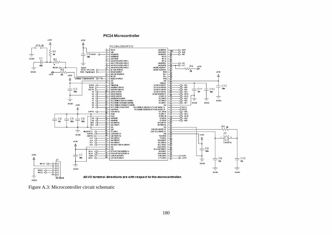
180
Figure A.3: Microcontroller circuit schematic

181
Figure A.4: WLAN connectors and parallel memory circuit schematic

182
Figure A.5: Bipolar ADC circuit schematic
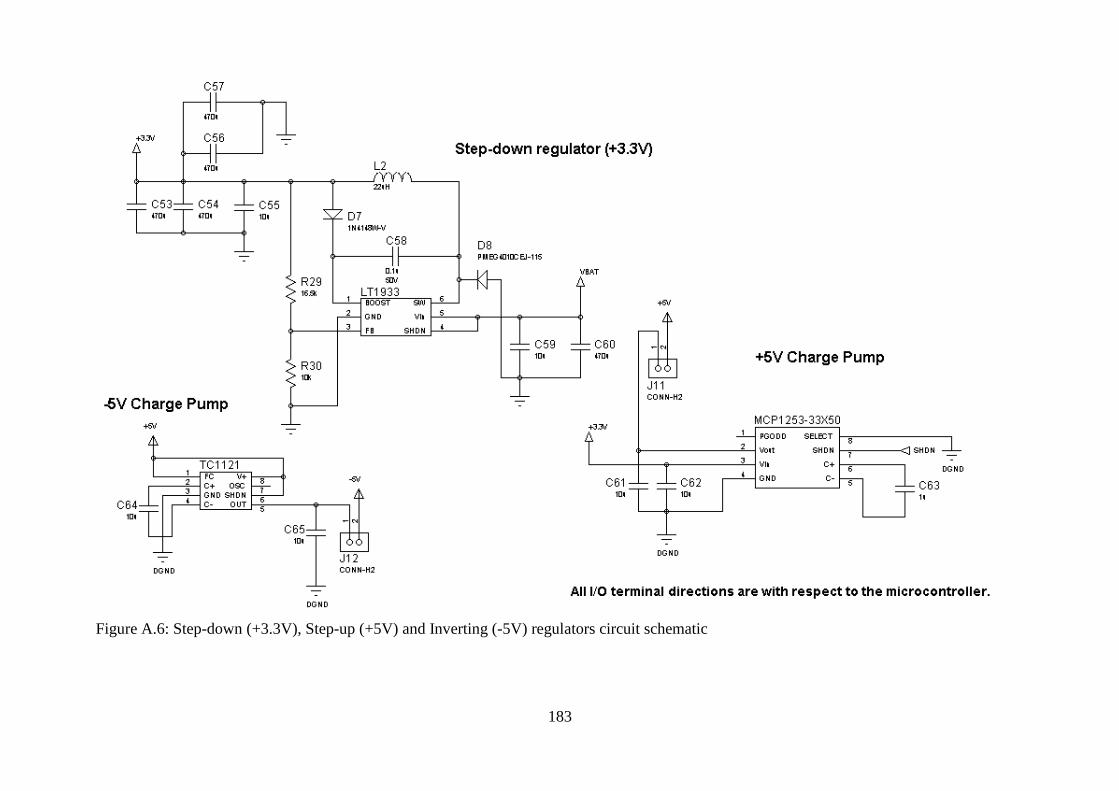
183
Figure A.6: Step-down (+3.3V), Step-up (+5V) and Inverting (-5V) regulators circuit schematic

184
Figure A.7: Solar powered battery charger circuit schematic

185
Table A.1: Bill of Materials
Category Quantity Reference Value
Unit Cost
(£)
Total Cost
(£)
Resistors 6 R1,R3-R6,R30 10k 0.008 0.128
Resistors 1 R2 1k 0.008 0.008
Resistors 1 R7 220 0.008 0.008
Resistors 5 R8,R9,R14,R15,R29 16.5k 0.009 0.045
Resistors 4 R10,R11,R16,R17 22.6k 0.009 0.036
Resistors 4 R12,R13,R18,R19 61.9k 0.009 0.036
Resistors 1 R20 470k 0.008 0.008
Resistors 3 R21,R22,R26 100k 0.008 0.024
Resistors 2 R23,R24 3k 0.008 0.016
Resistors 1 R25 0.05 0.35 0.35
Resistors 1 R27 64.9k 0.009 0.009
Resistors 1 R28 210k 0.008 0.008
Capacitors 19 C1-C3,C5-C8,C12,C13,C15,C17-C19,C27,C35,C37,C39,C41,C43 100n 0.006 0.114
Capacitors 17 C4,C11,C14,C20,C28,C36,C40,C42,C44,C47,C51,C55,C59,C61,C62,C64,C65 10u 0.023 0.391
Capacitors 2 C9,C10 22p 0.015 0.03
Capacitors 3 C16,C49,C63 1u 0.015 0.045
Capacitors 6 C21,C23,C25,C29,C31,C33 1n 0.015 0.09
Capacitors 2 C22,C30 820p 0.015 0.03
Capacitors 2 C24,C32 510p 0.015 0.03
Capacitors 2 C26,C34 68p 0.015 0.03
Capacitors 3 C38,C45,C48 680n 0.015 0.045
Capacitors 6 C46,C53,C54,C56,C57,C60 470u 0.292 1.752
Capacitors 1 C50 220u 0.186 0.186

186
Table A.2: Bill of Materials - continued
Category Quantity Reference Value Unit Cost (£) Total Cost (£)
Diodes 2 D2,D5 CD214A-B340LF 0.21 0.42
Diodes 1 D3 LED-RED 0.23 0.23
Diodes 2 D1,D4 LED-GREEN 0.138 0.276
Diodes 2 D6,D8 PMEG4010CEJ-115 0.062 0.124
Diodes 1 D7 1N4148W-V 0.036 0.072
Miscellaneous 2 J3,J4 M22-6112022 0.88 1.76
Miscellaneous 1 J1 SIL-100-06 0.344 0.344
Miscellaneous 5 J2,J5,J9,J11,J12 CONN-H2 0.098 0.49
Miscellaneous 5 Jumper 0.109 0.545
Miscellaneous 2 J6,J7, J8 SIL-100-02 Not installed Not installed
Miscellaneous 1 J10 Terminal block 2 way 0.46 0.46
Miscellaneous 1 Crimp housing 22-01-2025 0.20 0.20
Miscellaneous 2 Crimp 08-50-0032 0.06 0.12
Miscellaneous 1 L1 10uH 2.27 2.27
Miscellaneous 1 L2 22uH 0.82 0.82
Miscellaneous 1 NTC 10k 0.149 0.149
Miscellaneous 1 X1 CRYSTAL 0.458 0.458
Miscellaneous 2 GDS 0.714 1.428
Miscellaneous 2 MOV 0.119 0.398
Miscellaneous 2 TVS 0.864 1.728
Miscellaneous 2 BNC connector 1.17 1.17
Miscellaneous 1 Socket 2-way PFG.M0.2GL.AC52NZ 10.42 10.42
Miscellaneous 1 Cable plug 2-way PNG.M0.2GL.LN 8.94 8.94
Miscellaneous 1 Reverse-SMA to U.FL 4.87 4.87

187
Table A.3: Bill of Materials - continued
Category Quantity Reference Value Unit Cost (£) Total Cost (£)
Miscellaneous 1 Aluminium enclosure 1457N1601 20.18 20.18
Miscellaneous 4 Battery holder BK-18650-PC2-ND 1.177 4.71
Miscellaneous 4 Lithium-ion battery 18650, Tenergy Corp. 4.588 18.352
Miscellaneous 1 Printed circuit board 3.50 3.50
Miscellaneous 1 „Rubber ducky‟ 2.4GHz antenna 6.79 6.79
Miscellaneous 1 MSX-20 Solar panel 218.43 218.43
Integrated Circuits 2 LTC2052HVHGN 4.24 8.48
Integrated Circuits 1 CY7C1021DV33 1.73 1.73
Integrated Circuits 1 LT3652 5.47 5.47
Integrated Circuits 1 MCP1253-33X50 1.62 1.62
Integrated Circuits 1 TC1121 1.47 1.47
Integrated Circuits 1 PIC24HJ256GP210 5.67 5.67
Integrated Circuits 1 AD7367-5 7.93 7.93
Integrated Circuits 1 IRF7707PBF 0.61 0.61
Integrated Circuits 1 LT1933 3.67 3.67
Integrated Circuits 1 Matchport b/g 42.644 42.644
Total Wireless Sensor Cost 392.367

188
Appendix B
a) Time window 0-75 seconds b) Time window 75-150 seconds
c) Time window 150-225 seconds d) Time window 225-300 seconds
e) Time window 300-375 seconds f) Time window 375-450 seconds
g) Time window 450-525 seconds h) Time window 525-600 seconds
Figure B.1: Peak leakage current characteristic for the healthy polluted insulator

189
a) Leakage current peak value b) RMS of leakage current
c) RMS of applied voltage d) THD of leakage current
e) THD of applied voltage f) Average power
g) Accumulated Energy
Figure B.2: Operating voltage and leakage current characteristics for a healthy
polluted insulator measured using the DAQ card

190
a) Time window 0-75 seconds b) Time window 75-150 seconds
c) Time window 150-225 seconds d) Time window 225-300 seconds
e) Time window 300-375 seconds f) Time window 375-450 seconds
g) Time window 450-525 seconds h) Time window 525-600 seconds
Figure B.3: Peak leakage current characteristic for the damaged polluted insulator
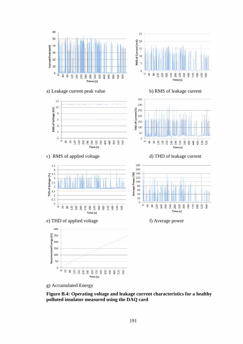
191
a) Leakage current peak value b) RMS of leakage current
c) RMS of applied voltage d) THD of leakage current
e) THD of applied voltage f) Average power
g) Accumulated Energy
Figure B.4: Operating voltage and leakage current characteristics for a healthy
polluted insulator measured using the DAQ card

192
Appendix C
Airpcap Tx
Airpcap Tx enables wireless network troubleshooting software like Wireshark to
provide information about the 802.11 wireless protocol and radio signals. AirPcap Tx
captures and analyze 802.11b/g wireless traffic, on a Windows PC or laptop. The
Airpcap Tx can only measure one 802.11 channel at a time and has an internal antenna,
with no option of connecting an external antenna to the device.
Wireshark
Wireshark is a free network protocol analyzer software, which allows capture
and interactive browsing of the traffic running on a wired or wireless network. In this
work AirpCap Tx was used in conjunction with Wireshark to capture wireless 802.11
traffic on the channel the WLAN Sensor was transmitting on. Captured and analyzed
Wireshark 802.11 packets were exported to Microsoft Excel 2007 for further analysis.
Cascade Pilot Personal Edition
Riverbed Cascade Pilot Personal Edition is a visually rich and powerful analyzer
for wired and wireless networks by providing capabilities not found in Wireshark.
While Pilot PE, like Wireshark, can also capture wired or wireless traffic it also offers a
large collection of analysis and plotting functions specifically designed to help
troubleshoot wired and wireless networks. In this work Cascade Pilot PE was used to
analyze and tabulate the amount of data transmitted from other 802.11 networks in the
vicinity of the WLAN sensor. It was also used to analyze and plot the signal strength
and transmission frame rate of the wireless transmitted data.
Wi-spy 2.4x USB adapter
The 2.4GHz spectrum was measured using the Wi-spy 2.4x USB adapter and the
spectrum analysis software Chanalyzer Pro. In this work the Wi-Spy 2.4x along with the
Chanalyzer Pro software was used to measure the 2.4GHz ISM frequency content. This
was done in order to discover which channels were noisy and identify potential
interfering devices.
Chanalyzer Pro
The Wi-spy 2.4x adapter was used in conjunction with the Chanalyzer Pro
software to measure the frequency content of the 2.4-2.5GHz spectrum. A number of
figures are available in Chanalyzer Pro that display the frequency content data measured
by the Wispy 2.4x adapter. In this work signal strength amplitude over time was plotted
using Chanalyzer Pro and the channel utilization factor and access points seen during
the measurement period, was tabulated.
While Wi-spy 2.4x measures the 2.4-2.5GHz spectrum, Chanalyzer Pro still
requires an 802.11 device to record the number of access points seen during

193
measurement. For example, Chanalyzer Pro requires the use of a PCs onboard 802.11
device, or an 802.11 USB adapter, to record all 802.11 access points in the vicinity.
Figure C.1: Waterfall view showing 1 minute of 2.4-2.5GHz spectrum
measurements - Llanrumney test field
Figure C.2: Density View showing 1 minute of 2.4-2.5GHz spectrum measurements
- Llanrumney test field
The Density View maps and displays how often a frequency/amplitude point is
being used. The less trafficked frequency ranges will appear more transparent. The
colors represent amplitude height with reds indicating higher signals and darker blues
lower power levels. An important feature of this view is that it picks up device-specific
signatures which enables analysis of what types of electronics are emitting RF energy in
the area.
Frequency (MHz)

194
While Passive Infrared (PIR) sensor products are commercially available that
also transmit in the 2.4GHz spectrum, none of such kind, were found to operate at the
Llanrumney field site or at the Cardiff universitiy‟s high voltage laboratory. While
Figure C.2 above, shows the outline of a PIR device, a distinctive, bright colored line,
lasting a number of seconds, at around 2.415GHz, would also be expected in Figure C.1
above. As no such bright colored line can be seen, this is further proof that the detection
of a „PIR – Security Device‟ flagged by Chanalyzer Pro was a false detection.
During every test that is presented in Chapter 7, a number of 802.11 networks
were detected and a very small number of „PIR Security Device‟, „ZigBee‟ and
„Wireless Camera-PAL‟ non-802.11 devices were also detected using the frequency
spectrum. As no amplitude values were observed in the waterfall figures, at the exact
time the „Display detected transmitters‟ function alerted to the detection of a non-802.11
device, they were all considered false detections.
Time (hh:mm)
Figure C.3: Signal strength of DI-524 access point measured at WLAN Sensor -
Llanrumney field test

195
Figure C.4: Waterfall view of 2.4-2.5GHz spectrum - Llanrumney field test
Time (hh:mm)
Figure C.5: Signal strength of DI-524 access point measured at WLAN Sensor -
Llanrumney field test
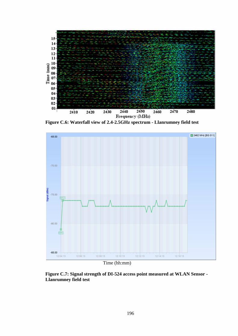
196
Figure C.6: Waterfall view of 2.4-2.5GHz spectrum - Llanrumney field test
Time (hh:mm)
Figure C.7: Signal strength of DI-524 access point measured at WLAN Sensor -
Llanrumney field test

197
Figure C.8: Waterfall view of 2.4-2.5GHz spectrum - High voltage laboratory
Time (hh:mm)
Figure C.9: Signal strength of DI-524 access point measured at WLAN Sensor -
High voltage laboratory

198
Figure C.10: Waterfall view of 2.4-2.5GHz spectrum - High voltage laboratory
Time (hh:mm)
Figure C.11: Signal strength of DI-524 access point measured at WLAN Sensor -
High voltage laboratory

199
Figure C.12: Waterfall view of 2.4-2.5GHz spectrum - High voltage laboratory
Time (hh:mm)
Figure C.13: Signal strength of DI-524 access point measured at WLAN Sensor -
High voltage laboratory

200
Figure C.14: Waterfall view of 2.4-2.5GHz spectrum – Damaged porcelain
insulator fog chamber test - High voltage laboratory
Time (hh:mm)
Figure C.15: Signal strength of DI-524 access point measured at WLAN Sensor -
Damaged porcelain insulator fog chamber test - High voltage laboratory
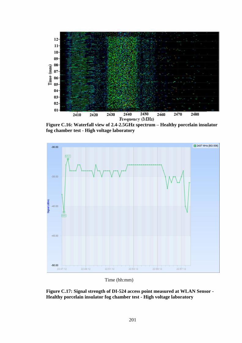
201
Figure C.16: Waterfall view of 2.4-2.5GHz spectrum – Healthy porcelain insulator
fog chamber test - High voltage laboratory
Time (hh:mm)
Figure C.17: Signal strength of DI-524 access point measured at WLAN Sensor -
Healthy porcelain insulator fog chamber test - High voltage laboratory