Embed Size (px)
Citation preview
Thickness determination and GB examination in polycrystalline samples
1
A tool for local thickness determination and grain boundary
characterization by CTEM and HRTEM techniques
Á.K. Kiss1, 2
, E. F. Rauch3, B. Pécz
1,2, J. Szívós
1, 2, J.L. Lábár
1
1 Hungarian Academy of Sciences, Research Center for Natural Sciences, Institute for Technical
Physics and Materials Science, Konkoly Thege M. út 29-33, H-1121 Budapest, Hungary
2 Doctoral School of Molecular-and Nanotechnologies, University of Pannonia, Faculty of
Information Technology, Egyetem u. 10., H-8200 Veszprém, Hungary
3 SIMaP, Grenoble INP/CNRS, 1130 rue de la Piscine - BP 75 - F-38402 St Martin D’Heres,
France
Keywords: thickness determination, grain boundary (GB), grain boundary
plane, high resolution (HRTEM)
Corresponding author: [email protected]

Thickness determination and GB examination in polycrystalline samples
2
Abstract
A new approach to the measurement of the local thickness and characterization
of grain boundaries is presented. The method is embodied in a software tool that helps
finding and setting sample orientations useful for high resolution transmission
electron microscopy examination of grain boundaries in polycrystalline thin films.
The novelty is the simultaneous treatment of the two neighboring grains and orienting
both grains and the boundary plane simultaneously. The same metric matrix based
formalism is used for all crystal systems. Input to the software tool includes
orientation data for the grains in question, which is determined automatically for a
large number of grains by the commercial ASTAR program. Our software also helps
identifying grains in a noisy orientation map. The grain boundaries suitable for
HRTEM examination are automatically identified by our software tool. Individual
boundaries are selected manually for detailed HRTEM examination from the
automatically identified set. Goniometer settings needed to observe the selected
boundary in HRTEM are advised by the software. Operation is demonstrated on
examples from the cubic and hexagonal crystal systems.
Introduction
Characterization of crystalline material in a transmission electron microscope
(TEM) necessitates tilting the sample to well defined crystallographic orientations
irrespective of the fact, if diffraction studies, conventional bright field (BF) or dark
field (DF) imaging or high resolution (HR) imaging is applied. Systematic tilting
operations are based on determining the orientation of the crystal with respect to the
laboratory system and also calibrating the orientations of the tilting axes of the
Thickness determination and GB examination in polycrystalline samples
3
goniometer relative to the same laboratory system. Determination of the orientation
can be based on convergent beam electron diffraction (CBED) patterns (Edington,
1975) or on electron diffraction patterns recorded with parallel nanobeams (NB). For
example CBED based orientation determination is implemented in the
ProcessDiffraction program (Lábár, 2005) and NB based orientation maps are
measured with the scanning-diffraction method (Rauch et al., 2008). An example of a
tilting tool that pre-calculates the tilting values needed to reach a desired crystal
orientation is the K-space Navigator program that also implements the tilts
automatically, using piezoelectric actuators of the goniometer (Duden et al., 2011).
Many studies are published where such tilting is applied for the examination of
nanocrystalline materials by high resolution techniques, e.g. the atomic arrangement
was explored within the crystals and the shape of the nanocrystals was determined in
order to understand their growing mechanism. The cornerstone of all these
experiments was the investigation of a chosen crystalline in many discrete low index
orientations (Jinschek et al., 2008, Van Aert et al., 2011, Gontard et al., 2008, Habas
et al., 2007). The accurate computer-control of the sample holder by Duden et al.
(Duden et al., 2011) allowed orienting individual crystallites of nanometer size with
high accuracy (Habas et al., 2007). Thus their software navigates in the reciprocal
space – while the operator stays in real space imaging mode during the tilting
operation so he/she can keep the examined area stationary (by correcting for
unwanted shifts if needed).
When grain boundaries are to be examined, the situation is more complex since
three related entities must be oriented simultaneously: both grains and the boundary
plane between them. The software tool that we report here offers a solution to that
more complex problem.

Thickness determination and GB examination in polycrystalline samples
4
The macroscopic properties of a GB are described by 5 parameters (5 degrees of
freedom) namely the 3 parameters giving the relative crystallographic difference
between their orientations (i.e. misorientation) and the 2 parameters describing the
orientation (normal vector) of the crystallographic plane of the grain boundary (GB)
between them (Randle, 1993). In that description even curved GBs are approximated
locally by planes. That approximation is valid even for GBs with significant curvature
(Forwood & Clarebroug, 1991). The orientation of any individual crystallite means
the relation between its native crystallographic system and the laboratory system i.e.
corresponds to a coordinate-transformation that can be represented by an orientation-
matrix. The misorientation between two grains is defined as a rotation transformation
between the two Cartesian coordinate systems attached to the native crystallographic
systems of the neighboring grains so it is deduced from the orientation matrices. The
coincidence site lattice theory (CSL-theory) describes the misorientation of the
neighboring grains for special low energy arrangements (Grimmer et al., 1974) but
does not specify the orientation of the boundary plane between them.
Determination of the orientation of the boundary plane is more tedious than
determination of the orientations of crystallites (grains). Such studies are frequently
carried out in scanning electron microscopes (SEM) using electron backscatter
diffraction (EBSD). In the simplest version of that method an orientation map of the
grains is recorded with EBSD and direction of the surface line traces of GBs are
identified. Since an infinite number of GB orientations can result in the same surface
line trace, the method gives an incomplete characterization of the GB (Saylor et al.,
2004). However, measuring only the orientation of the line trace of the GB-plane can
be applied to decide whether the GB can be a special one or not (e.g. in case of Σ3
misorientation: can the GB be {111}-like or not.) (Randle, 2001). Complete

Thickness determination and GB examination in polycrystalline samples
5
characterization applies a tedious 3-dimensional (3D) EBSD approach. First an EBSD
map is recorded then a very thin layer of fixed thickness is removed (parallel to the
original surface). These two steps are cycled and the 3D distribution of boundaries is
reconstructed from following the virtual shift of the GB line traces as a function of
depth (Saylor et al., 2003).
In this paper we show complete characterization of GBs with a semi-automatic
procedure in the TEM. Although not completely automatic and concentrates only on a
small number of boundaries at a time, our approach is easier than the one applying the
3D EBSD / FIB technique and provides a more complex operation than the methods
orienting a single grain only. Subsequent to the macroscopic characterization we can
also investigate selected GBs with HRTEM.
Our approach determines the orientation of the GB plane from the projected
image of the polycrystalline thin film in the TEM. Whenever the GB plane is oriented
oblique to the electron beam both the upper and the bottom line traces of the GB plane
are discerned in the projected image and using the known local thickness of the thin
film the elevation of the GB plane can be deduced. Local thickness can be determined
from CBED for thicker crystalline samples (Kelly, 1975) or from comparing
simulated HRTEM images to experimental ones (Stadelmann, 1987) in case of the
thinnest films. As an alternative, the thickness of the sample can also be determined
by electron energy loss spectrometry (EELS) (Egerton, 2011). Although the upper and
lower traces can be told apart from the variation of the contrast for special GBs
(Edington, 1976) in thicker films, we apply the more general method of stereographic
reconstruction from a couple projections recorded with different tilts. The thickness of
the sample was a necessary input parameter in our previous measurements (Lábár et
al., 2012, Kiss et al., 2013), while the thickness is one of the variables determined as

Thickness determination and GB examination in polycrystalline samples
6
an integral part of our recent method presented in this paper. We only take the
crystalline phase into account here, while any contamination or amorphous supporting
layer has no impact on our thickness determination in contrast to the thickness value
obtained by the EELS method.
However, for HRTEM the investigated area of the sample must be clean i.e. free
of any contamination and must not be thicker than a few tens of nanometers.
Furthermore, the investigated crystal have to be well oriented, the electron beam is
only allowed to be parallel to low-index crystallographic directions. A manual
orientation exercise based on diffraction requires practice from the TEM-operator.
During tilting the sample, the investigated area may go out of focus and can also slide
out of the viewing range. Therefore the final tilt position is usually reached after many
tilt and correction cycles. During that lengthy procedure the illuminated area may be
contaminated and become useless for HRTEM (Egerton et al., 2004). That is why the
computer aided tilt procedure is needed.
Characterization is performed in three steps in our approach. First an orientation
map is collected in the TEM with ASTAR (Rauch et al., 2008,
http://www.nanomegas.com/). Grains with lateral size of > 20 nm can be mapped in
our LaB6 TEM and many grains are evaluated in a single map. (Probe size and
consequently the measurable grain size are limited by the brightness of our TEM and
the need that a grain must extend several pixels.) Having an orientation map for many
grains simultaneously is particularly important for finding GBs for HRTEM, since
only a low fraction of all GBs are oriented in a direction that facilitates tilting the GB
plane parallel to the electron beam due to the limited tilting range of the goniometer.

Thickness determination and GB examination in polycrystalline samples
7
Steps of the procedure
Calibration of the microscope
Pre-calculation of the needed tilt values in a double tilt holder needs two
calibrations.
a) Rotation of the diffraction pattern relative to the image must be calibrated as a
function of magnifications and the camera lengths used (Loretto & Smallman,
1975).
b) In order to control the sample holder properly, the directions of its tilt-axes
have also to be known in the laboratory system. These can be measured e.g. by
studying the shift of a convergent beam electron diffraction (CBED) pattern
while tilting the sample. The line trace of motion of the image of an arbitrary
zone axis (the crossing point of Kikuchi-bands) assigns clearly the plane of the
tilt, thus the axis of the rotation.
Characterization of the GB plane from its projection and
calculation of the local thickness in the TEM
The orientation of a GB-plane is given by its normal vector. That normal vector
(expressed in the laboratory system), and also the local thickness of the sample can be
determined from either bright-field (BF) images (for thicker samples) or form HR
images (for thin samples) of the GB. Both the width and the direction of the
projection of the GB-plane have to be measured on BF images (Fig. 1), while the
corresponding tilt-values of the double-tilt sample holder (goniometer) are input
parameters of the calculation. Fig. 2 shows a schematic cross section of the sample

Thickness determination and GB examination in polycrystalline samples
8
containing a GB. All the notations used in this paper are consistent with the ones
marked in the Fig. 1 and Fig. 2.
The laboratory-coordinate-system (image-system) is defined as follows:
X-direction: lies in the image plane, pointing right.
Y-direction: lies in the image plane, pointing upward.
Z-direction: points perpendicular to the image plane, against the reader.
d – Width of the projection of the GB.
δ – The angle indicating the direction of the projection of the GB in the image
plane. This angle is measured from the X-direction in positive manner. δ = 0…180°
ntrace – Unit vector, which is normal to the projection of the GB. It lies in the
image plane. Its components are calculated with the help of d and δ.
The cross section of the sample described in Fig. 2 (i.e. the plane of the figure)
lies perpendicular to the image plane and also perpendicular to the projection of the
GB (i.e. parallel to ntrace).
b – The part of the GB lying in the plane of the cross-section indicated in Fig. 2.
nGB – Unit vector, normal to the plane of the GB.
t – Thickness of the sample.
ω – The angle between the sample-surface and the GB-plane. ω = 0°…180°
Since either the width or the direction of the projection of a GB do not change
while tilting the sample about an axis lying parallel to ntrace, the tilt positions of the
sample differing only in a rotation component about this axis are experimentally
equivalent. Therefore we consider all the tilt positions as they were tilted only about
an axis parallel to the projection of the GB. This is how α can be calculated:

Thickness determination and GB examination in polycrystalline samples
9
α – the angle between the sample-surface and the image plane in the
aforementioned manner. α = -90°…+90° If β is the angle between ntrace and the
normal direction of the sample, then:
𝛼 = 90° − 𝛽
At the zero-tilt position the normal direction of the sample-surface corresponds
to the unit vector pointing in the Z-direction. Since the directions of the tilt axes of the
sample-holder are known, the normal of the sample-surface can be easily calculated.
According to Fig. 2, the following equations can be written with the variables of
t and ω:
(eq. 1)
{cos(𝛼 + 𝜔) =
𝑑
𝑏
sin(𝜔) =𝑡
𝑏
→ t ∙ cos(𝛼 + 𝜔) = 𝑑 ∙ sin(𝜔)
Therefore the following equation system has to be solved for t and ω, where the
input parameters d1, α1 and d2, α2 come from measurements based on two different tilt
positions:
(eq.2)
{t ∙ cos(𝛼1 + 𝜔) = 𝑑1 ∙ sin(𝜔)
t ∙ cos(𝛼2 + 𝜔) = 𝑑2 ∙ sin(𝜔)
Thus (here t can be expressed both with d1, α1 or d2, α2):
(eq.3)
cot(𝜔) =𝑑1 sin(𝛼2) − 𝑑2 sin(𝛼1)
𝑑1 cos(𝛼2) − 𝑑2 cos(𝛼1)
(eq. 4)

Thickness determination and GB examination in polycrystalline samples
10
𝑡 =𝑑1|2
cot(𝜔) ∙ cos(𝛼1|2) − sin(𝛼1|2)
Fig. 1. Schematic illustration of the projection of a GB in the image. The trace is
illustrated by the gray band its width and direction are characterized by d and δ,
respectively. The normal direction of the projection (ntrace) is expressed by these
measured values.

Thickness determination and GB examination in polycrystalline samples
11
Fig. 2 Schematic cross section of a TEM-sample containing a grain boundary.
Fig. 3 shows, that both a right and a left tilted GB can produce the same
projection in the image plane. If it is not identified, which edge of the projection
belongs to the upper and which to the lower surface of the sample, due to this
ambiguity, the value of cos(𝛼 + 𝜔) in (eq. 1) can be either positive or negative.
Therefore the measured widths of the projections have to be tested with both positive
and negative sign of cos(𝛼 + 𝜔). Thus (eq. 2) have to be evaluated in four ways,
since we have no prediction about that, what sign of cos(𝛼 + 𝜔) the measured d
values have to be substituted with. Two1 of the four solutions describe physically
possible cases resulting in positive values for the sample thickness. These solutions
are illustrated in Fig. 4. In practice, if one solution for the local thickness can be
rejected, because it can physically be ruled out (e.g. so thick that it could not be
1 According to (eq. 3) and (eq. 4), when both d1 and d2 change sign, cot(ω) will not change and t
will change sign. Therefore the four solutions for t contains two pairs, each with equal absolute values
but with positive and negative sign.

Thickness determination and GB examination in polycrystalline samples
12
transmitted by the electrons) then only one solution for t is left, thus the elevation of
the GB-plane is determined unambiguously. If it is not, an additional measurement
with other tilt settings is needed: by evaluating (eq. 4) with the possible input data
pairs, the solution, common to the two data-pairs select the physical relevant values
for local thickness and the corresponding GB-plane. When the normal vector of the
GB is expressed in the laboratory system, the corresponding hkl indices of the plane
can be expressed in both native-systems of the neighboring grains with the help of a
linear transformation using the two orientation matrices (see following chapter).
To improve the accuracy of the measurements it is recommended to choose such
a goniometer setting in which the projection of the GB can be measured easily. In the
case of a relatively thick sample, one of the neighboring grains may be oriented in
two-beam condition: in this case there are thickness fringes2 in the projection of the
boundary result is sharp contrast at the edges of the projection (Fig. 5/a). When the
sample is prepared for HRTEM imaging, the thickness is too small for producing such
thickness fringes. In this case HRTEM can be used (see following chapters): since the
superposition of the neighboring line-periodicities appears in the overlapping area, the
edges of the projection can be measured with a good accuracy (Fig. 5/b).
2 The thickness fringes appear due to the wedge shaped part of the crystal cut by the grain
boundary.

Thickness determination and GB examination in polycrystalline samples
13
Fig. 3. Schematic illustration of the fact that both the right and the left tilted GBs
(marked by thick gray lines) can produce the same projection in the image plane.
Fig. 4. Schematic illustration of the tilt ambiguity of the GB-plane. Both of the two
kinds of samples (one with the thickness tI and the other with tII) produces the same

Thickness determination and GB examination in polycrystalline samples
14
projection in each of the two tilt positions (a), (b). Note that the elevation (ωI, ωII) of
the theoretical GBs are the same, constant in both (a) and (b).
Fig. 5. Bright field image taken on polycrystalline Si thin film (a) and HR image
taken on polycrystalline Al film (b). The azimuth angles and the width are marked.
The sharp contrasts of the projected GBs are significant. In the image (a), the grain
on the left hand side is oriented in two beam condition therefore the thickness fringes
are seen very well. In image (b), both of the neighboring grains are imaged with plane
resolution, resulting in well observable pattern in the overlapping area. Due to the
misorientation angle of 60° between the planes of the two grains by chance, the Moiré
pattern and a simple superposition look the same.
Measurement of orientation, orientation mapping
Evaluating a Kikuchi-band map on a CBED pattern is one of the most accurate
methods of the local measurement of orientation and we started by testing that method
manually on a selection of grains. However, for manual CBED measurements the

Thickness determination and GB examination in polycrystalline samples
15
local sample thickness has to be thicker than optimal for HRTEM. Additionally,
measuring the grains one-by-one is very time-consuming; thus this method does not
satisfy our need to collect many orientation data from a large area in reasonable time.
That is why the orientation maps were finally measured with the commercial Astar
scanning/precession tool (Rauch et al., 2008, http://www.nanomegas.com/). installed
on a JEOL 3010 HRTEM. That tool provides an orientation map from the area of
interest with reasonable accuracy in a quite short time (tens of minutes). Every pixel
in the orientation map contains local orientation and phase information about the
corresponding location of the sample, i.e. the three Euler-angles and a phase-index are
stored in each pixel. Since in the next step we use the orientation matrix formalism,
the Euler angles are converted into orientation matrices.
The orientation matrix (O) describes a direct connection between the direction-
coordinates expressed in the laboratory-system and in the native crystallographic
system:
nativLab rOr
The O orientation matrix can be written in the following way.
MNO 1
The N matrix is calculated from the φ, θ, ψ Euler-angles and gives the relation
between the laboratory-system and the virtual Cartesian-system attached to the native
crystal-system. Thus N matrix characterizes only the rotation of the grain compared to
the laboratory system without having any information about the crystal-structure. N
can be expressed by the Euler-angles (Randle, 1993):

Thickness determination and GB examination in polycrystalline samples
16
cos
sincos
sinsin
sincos
coscoscossinsin
coscossinsincos
sinsin
cossincoscossin
cossinsincoscos
2,2
1,2
0,2
2,1
1,1
0,1
2,0
1,0
0,0
N
N
N
N
N
N
N
N
N
The M matrix describes the relation between the native crystallographic-system
and the Cartesian-system attached to the grain. The M matrix is expressed by the
native cell-parameters:
sin
coscoscos2coscoscos1
sin
coscoscos
cos
0
sin
cos
0
0
222
2,2
1,2
0,2
2,1
1,1
0,1
2,0
1,0
0,0
cM
cM
cM
M
bM
bM
M
M
aM
Here a, b, c are the lengths of the lattice-vectors, α, β, γ are the opposite angles
of the unit cell. The x, y, z Cartesian-system attached to the native system is created
following one of the usual crystallographic conventions (International tables for
crystallography Vol. B, 2001) (Fig. 6):

Thickness determination and GB examination in polycrystalline samples
17
x║a;
y┴x and lies in the plane defined by a,b;
z║c*
Fig. 6. The relation between the native crystallographic-system and the attached
Cartesian-system.
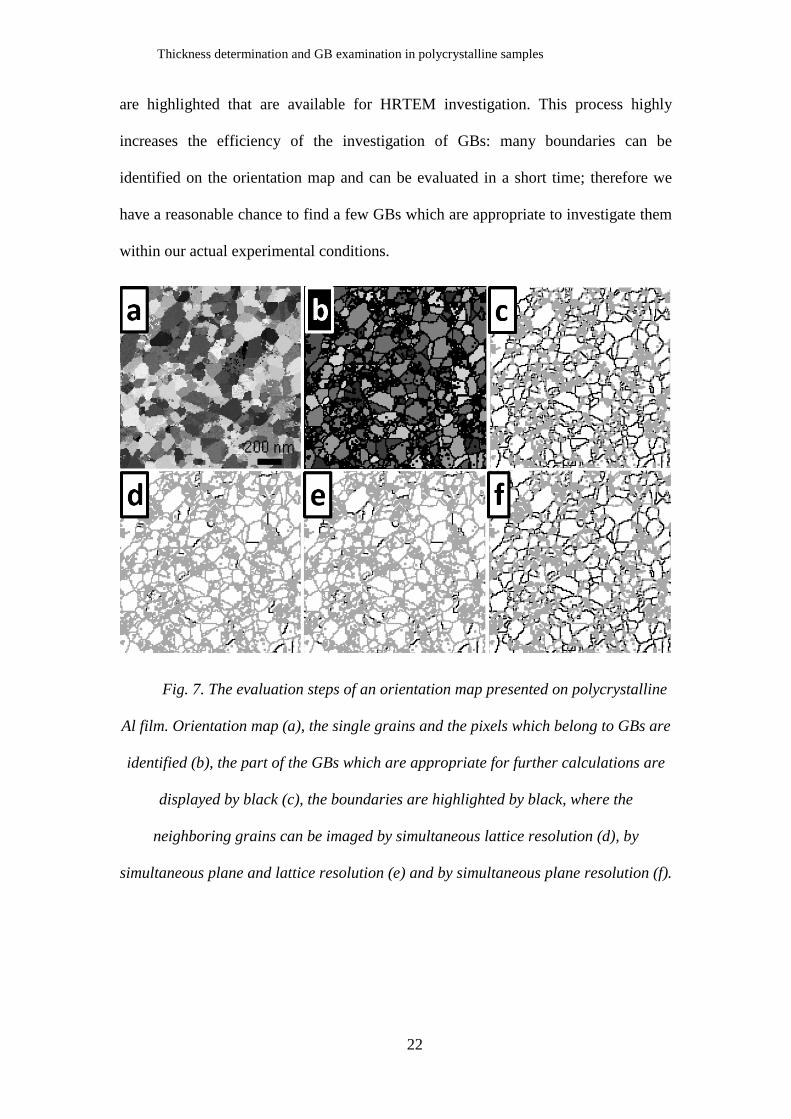
Automatic identification of the grains; noise reduction
The primary input to our software that identifies grains and grain boundaries is a
pixel-by-pixel orientation map (Fig. 7/a). By visual inspection of the colored
orientation map we have a rough idea about the extension of the grains. However, due
to noise and the occasionally low reliability of indexing it is not perfectly obvious
which pixels belong to a grain and which pixels belong to the next grain and which
ones to the GB between them. Our software first classifies each pixel to yield grain
areas with (a common, approximately) homogeneous orientations and GB areas
between them.

Thickness determination and GB examination in polycrystalline samples
18
Classification is based on the fact that at least one Euler angle must change
significantly as a GB is crossed. So, we display the three Euler-angles in three
separate images where each pixel contains the corresponding value of displayed
Euler-angle. Then we apply the “Sobel” edge-detection method (Sobel, I., 1978, Qu
Ying-Donga et al., 2005) on each of the three images one-by-one. As a result, in all
three images the procedure highlights the pixels that are situated in a region where the
displayed Euler angle changes significantly. The edges, detected on these 3 images
are combined, resulting in a single GB-map. The contrast in the GB map is related to
the angular change across the GB. This means that the high-angle boundaries appear
with stronger contrast than the low-angle boundaries. If we do not want to sub-
classify the GBs, only detect them then all edges above a threshold intensity level are
accepted as GB pixels. The pixels with lower (than the threshold) contrast will be set
white and the pixels with higher contrast will be set black, therefore the noise within
the grains can be filtered out and in the case of a low threshold value both the low-
angle boundaries and the high-angle boundaries are identically highlighted. If the
threshold is increased to about 15° only high angle boundaries are identified.
Next the grains in this black-and-white GB-map are given unique sequence
numbers. All the white pixels that belong to the same grain get the same unique
sequence number (Fig. 7/b). Referring to each grain by its own sequence number,
both a phase index and an average orientation will be assigned to each grain. The
average orientation is calculated by averaging the Euler-values stored in the grain’s
pixels. Thus unique orientation matrices are assigned to each grain. Next, all data
belonging to both neighboring grains are stored for the pixels of the GB between them
(Fig. 7/c). That approach must be useful in characterizing either grain boundaries or

Thickness determination and GB examination in polycrystalline samples
19
phase boundaries. (Obviously, this approach is not intended to be used to characterize
in-grain curvature, twist, etc.)
Next the average orientation data of the grains are compared to the orientations
of each of their neighbors: in case of finding appropriate pairs, the GB-pixels
containing the same neighbor-grain sequence numbers will be highlighted.
For the favorable case when both grains can be tilted to zone axis direction for
examination, the tilt-angles needed to orient those zones in beam-direction are
calculated for those pairs, which are simultaneously within the tilting range of the
sample holder. That procedure is straightforward. The question still remains if any of
these zone axis pairs lie parallel to the respective GB plane.
In the worst case scenario when only one plane per grain can be resolved we
find the needed common orientation with a different algorithm. We find all the hkl
indexes, which are representing resolvable sets of crystal planes. First the real space
direction [nmp] is found that is parallel to the hkl-directions of the reciprocal-space
using the metric-tensor (G) of the given crystal structure (Spence, 1992).
l
k
h
G
p
m
n1
ccbcac
cbbbab
cabaaa
G
Here m,n,p are indices in direct-space, h,k,l are indices in reciprocal-space
(Miller-indices) and a, b, c are the base-vectors of the real space lattice.

Thickness determination and GB examination in polycrystalline samples
20
Now these normal vectors of planes (given in the direct-space native crystal
system) are transformed into the laboratory system and we can build pairs where the
first member of the pair comes from the first grain, the second one comes from the
other. After the cross-product was calculated for a pair, the resulting direction may be
tilted parallel to the electron beam. (Since the laboratory system is a Descartes system,
parallel directions in real space and reciprocal space are characterized with the same
indices.) From that direction we can take an HRTEM image in which one plane per
grain is resolved simultaneously.
Our software searches automatically all neighboring grain pairs and highlights
their boundary when they can be tilted for HRTEM taking into account the tilting
limits of the sample holder. By double-clicking on a highlighted GB the accessible
zones or planes are listed together with the needed tilt values. Subsequently the tilting
operation is done in imaging mode and the grains are kept stationary by the operator.
It is important to note that both the identification of the orientation and the tilt
operation is of finite accuracy. First, the orientation is determined from a search-
match algorithm by ASTAR where the measured pattern is matched to a set of pre-
calculated patterns (templates). Templates are usually calculated in 1° steps.
Additionally the accuracy of our goniometer is about 0.2°. Additionally, small
orientation changes can also be present within the grains due to the presence of
dislocations. As a consequence, fine-tuning of the tilt values are needed around the
calculated tilt values as show in the examples section.
Investigation of GBs by HRTEM
In order to get a lattice resolution image on the chosen crystal with more than
one lattice planes resolved simultaneously, the beam must be parallel to a low index

Thickness determination and GB examination in polycrystalline samples
21
zone axis direction (the number of available zones depends on the point resolution of
the microscope). When these low-index zone axis directions are out of the tilting
range of the sample holder, orienting only one set of resolvable planes parallel to the
beam can still be possible and a single lattice plane can be imaged up to the line
resolution of the HRTEM. When GBs are to be examined by HRTEM, preferably
several lattice planes should be imaged in each of the grains simultaneously and the
GB plane also should be set parallel to the electron beam at the same time. In the case
of a random orientation distribution of grains, there is little chance to find parallel
low-index zone axes in both neighboring grains, and the chance is even lower to find
them within the tilting range of the sample holder. So, occasionally it is impossible to
fulfill all these conditions simultaneously and no solution exists at all. In the least
favorable case one plane per grain is only resolved simultaneously and the GB plane
remains oblique to the electron beam. This last condition provides the minimal
information about the GB structure. Of course, the looser the expected experimental
conditions are, the more boundaries will be accessible for examination (Fig. 7/d,e,f).
Any of the above HRTEM situations are difficult to find manually and we must be
very lucky to find an appropriate pair of grains in a polycrystalline sample without the
help of a computer.
Our software tool helps to find these appropriate GBs in a polycrystalline thin
film and gives advice how to tilt the double-tilt sample holder in order to obtain high
resolution images. First an orientation map is recorded with the help of the Astar
scanning/precession tool installed on the HRTEM, and then our software processes
the orientation map, also using the actual experimental conditions, such as the
resolution limit of the microscope, the directions of the tilt axes in the laboratory
system and the value of the maximal available tilt. On the resulting GB-map the GBs
Thickness determination and GB examination in polycrystalline samples
22
are highlighted that are available for HRTEM investigation. This process highly
increases the efficiency of the investigation of GBs: many boundaries can be
identified on the orientation map and can be evaluated in a short time; therefore we
have a reasonable chance to find a few GBs which are appropriate to investigate them
within our actual experimental conditions.
Fig. 7. The evaluation steps of an orientation map presented on polycrystalline
Al film. Orientation map (a), the single grains and the pixels which belong to GBs are
identified (b), the part of the GBs which are appropriate for further calculations are
displayed by black (c), the boundaries are highlighted by black, where the
neighboring grains can be imaged by simultaneous lattice resolution (d), by
simultaneous plane and lattice resolution (e) and by simultaneous plane resolution (f).

Thickness determination and GB examination in polycrystalline samples
23
Experimental demonstration of use
Application of our software tool is demonstrated on both a polycrystalline fcc
Al, and on hcp ZnO sample. The self-supporting Al layer was gown by DC magnetron
sputtering on thin amorphous carbon film supported by a copper TEM-grid. (The base
pressure was 1.6*10-7
mbar and the argon pressure during deposition was 2.5*10-3
mbar. Aluminium was sputtered at 100 W power for 5 min. The sample was annealed
at 250°C in 1.4*10-7
mbar for 30 min.) The investigations were made with a JEOL
3010 HRTEM equipped with an Astar scanning/precession device.
All the orientation maps presented in this paper are colored by the color code3
shown in Fig. 8. One of the basic directions (X: points to the right, Y: points upward
or Z: direction of observation, normal to the plane of the image) of the sample can be
selected to color code the orientation distribution of that direction in the orientation
map.
Fig. 8. Color coding in orientation maps for cubic and hexagonal structures.
3 For readers of the B/W printed version, it is only important that the different grains in Fig. 7/a,
Fig. 9/a, Fig. 13/a and Fig. 16 are shown with different shades.

Thickness determination and GB examination in polycrystalline samples
24
Example I.
In our first example the simplest case, a twin boundary with ∑3 misorientation
in a cubic material (Al) is shown. After an orientation map had been taken on the area
of interest, the boundaries have been highlighted where both neighboring grains can
be investigated in exact zone direction (Fig. 9, Fig. 10). The errors introduced by the
evaluation led to a non-negligible inaccuracy in the calculated values compared to the
refined experimental ones. The final tilt differs from the calculated tilt by 1-2°, and
the calculated orientation deviation (OD) between the two expected zone directions
achieves almost 1° (Table 1). Since the ∑3 misorientation predicts no OD, our
calculated results can only be attributed to the evaluation errors which have been
introduced by the inaccuracy of the orientation identification and by the bending of
the sample.
The grain size is about 100 nm and the orientation map has been collected with
10 nm spot size. After the tilt refinement both neighboring grains are imaged in exact
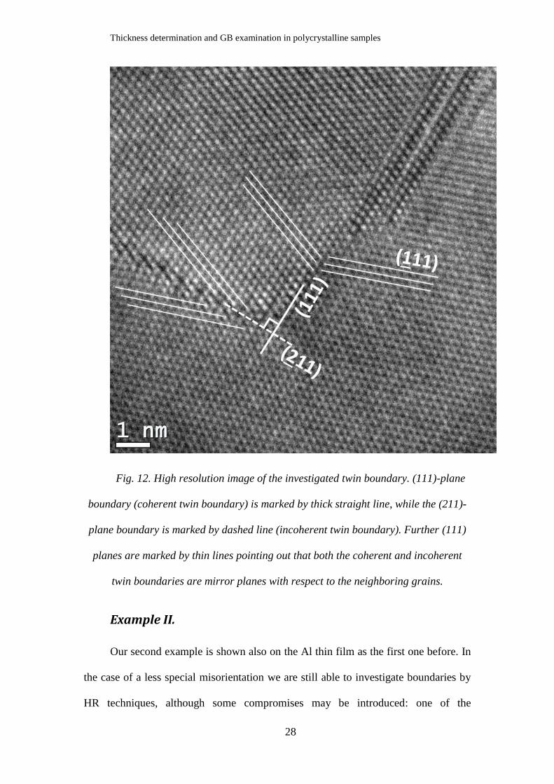
[110] zone directions (Fig. 11). The boundary plane has (111) characteristics
(coherent twin boundary) with perpendicular (211) steps (incoherent twin boundary)
(Fig. 12).
Table 1. Experimental conditions of HTEM imaging
Grain Zone to reach
Predicted OD (here
it is an indication
of calculation
error)
Calculated
tilt position
Refined tilt position
to simultaneous zone
axis orientation

Thickness determination and GB examination in polycrystalline samples
25
1 [110]
0.9°
-7.9°/9.6°
-6.4°/8.3°
2 [110] -7.1°/10°
Fig. 9. Orientation map of an Al foil – the coloring (shading) displays the
orientation distribution in the X-direction (a). The black-highlighted boundaries are
available for HRTEM imaging (b). The investigated boundary is marked by an arrow.

Thickness determination and GB examination in polycrystalline samples
26
Fig. 10. The studied grains shown with low magnification. The part of the boundary
investigated by high resolution is marked by the dashed rectangle.

Thickness determination and GB examination in polycrystalline samples
27
Fig. 11. High resolution image of the investigated twin boundary. The FFT
patterns are indicating the exact [110] zone orientation. The same type of zones are
rotated in the two grains.
Thickness determination and GB examination in polycrystalline samples
28
Fig. 12. High resolution image of the investigated twin boundary. (111)-plane
boundary (coherent twin boundary) is marked by thick straight line, while the (211)-
plane boundary is marked by dashed line (incoherent twin boundary). Further (111)
planes are marked by thin lines pointing out that both the coherent and incoherent
twin boundaries are mirror planes with respect to the neighboring grains.
Example II.
Our second example is shown also on the Al thin film as the first one before. In
the case of a less special misorientation we are still able to investigate boundaries by
HR techniques, although some compromises may be introduced: one of the

Thickness determination and GB examination in polycrystalline samples
29
neighboring grains is imaged in a zone direction showing lattice resolution, while in
the other one only one set of planes is resolved. Fig. 13/a shows the orientation map
of the investigated area, in Fig. 13/b those boundaries are lighted, where the
aforementioned experimental condition can be accomplished: the chosen GB is
marked by an arrow where one of the neighboring grains shows lattice resolution in
[110] zone and the other one shows plane resolution with (111) planes in accordance
with our prediction. In the Fig. 14/a1 and Fig. 14/b1 CBED images are presenting the
accuracy of the tilt calculations, while also the meaning of the calculated OD becomes
clear: these CBED images have been taken just after the sample had been oriented in
the calculated tilt position. The values of the calculated and the refined tilt positions
and the OD are detailed in the Table 2. Theoretically the calculated value of the OD
indicates how far a grain lies from the two-beam condition, while the other grain is set
in an exact zone position. In the case of a small value of that (<0.5°), both the lattice
and the plane resolution can be reached by an appropriate tilt refinement (see Fig.
14/a2 and Fig. 14/b2). The high resolution image4 is shown in the Fig. 15 when the
sample reached the final refined position.
4 The sample is of medium thickness, where both the Kikuchi bands can be seen after contrast
enhancement in the CBED and a HRTEM can also be seen, although with not the optimum quality.

Thickness determination and GB examination in polycrystalline samples
30
Fig. 13. Orientation map of an Al foil – the coloring displays the orientation
distribution in the X-direction (a). The black-highlighted boundaries are available for
lattice and plane resolution HRTEM imaging (b). The investigated boundary is
marked by an arrow.

Thickness determination and GB examination in polycrystalline samples
31
Fig. 14. CBED patterns taken on the investigated neighbors, while the sample
has been oriented to the calculated tilt position: one of the neighboring grains lies in
almost exact [110] zone position (a1), and the other one is near to a two-beam
condition (b1). CBED patterns has been taken at the same grains after the tilt
refinement (a2 and b2).
Table 2. Experimental conditions of HTEM imaging
Grain Zone or Predicted Calculated Refined tilt position to zone

Thickness determination and GB examination in polycrystalline samples
32
plane to set OD tilt position axis orientation in grain a
a [110]
0.47° 7.6°/7.1° 8.4°/7.8°
b (111)
Fig. 15. High resolution image of the investigated boundary. The FFT patterns
are indicating the exact [110] zone orientation in the upper grain and the (111)
planes at the bottom.

Thickness determination and GB examination in polycrystalline samples
33
Example III.
Our next example is presented here on an hcp ZnO thin film with grain size of
ca. 20-40 nm deposited on a Si substrate. Fig. 16 shows the orientation map of the
selected area. Different colors represent different orientations (the green area at
bottom5 is the Si substrate), therefore individual grains can be recognized. The chosen
boundary is marked by the white arrow. Fig. 17 shows high resolution image of the
observed boundary: one of the neighboring grains is imaged with lattice resolution
from [011] i.e. [-1 2 -1 3] zone direction, while only the (011) i.e. (0 1 -1 1) planes are
resolved in the other grain. In the area marked by the dashed rectangle no overlap is
seen; so the interface plane cannot be tilted too much away from the beam direction.
5 light shade in the B/W version

Thickness determination and GB examination in polycrystalline samples
34
Fig. 16. Orientation map from hcp ZnO – orientation distribution in the Z-
direction is displayed by the colors. The observed boundary is marked by the white
arrow.

Thickness determination and GB examination in polycrystalline samples
35
Fig. 17. The chosen boundary (from Fig. 15) shows no overlapping in the
indicated area, while the neighboring grains are imaged with lattice resolution
(viewed from [011] i.e. [-1 2 -1 3] zone) and plane resolution (showing the (011) i.e.
(0 1 -1 1) planes).
Example IV.
In our last example the aforementioned fcc Al thin film has been examined
again. The investigated boundary was intentionally tilted so that only one set of planes
per grain are resolved, with the aim in mind to determine simultaneously both the
indices of the GB plane and the thickness of the Al foil (Fig. 18). Note, that this kind
of experimental condition can be achieved quite often as it is illustrated by Fig. 7, so
this method of determining local thickness can be applied quite generally. As we

Thickness determination and GB examination in polycrystalline samples
36
mentioned before, this calculation needs at least two (but sometimes more than two)
independent measurements. In the present case we chose two GBs and did two
measurements per GB, each with different tilt positions. Although we got two
solutions per GB, the solution common to the two pairs selects the physically relevant
one resulting in 30 nm in thickness in the example. Note, that only the crystalline
phase has been taken into account for the calculation of thickness, while the presence
of the amorphous carbon supporting layer has no impact on it, in contrast to the
thickness measurement based on electron energy loss spectroscopy (EELS)
techniques.
Cross section of another Al thin film grown under identical conditions on an
oxidized silicone substrate has also been investigated (Fig. 19) for checking if the
implicit assumption in our calculation, namely that our layer can be regarded as a
plan-parallel slab is justified. Although the Al layer grown on Si the substrate proved
to be different6 in thickness, the top surface of the Al layer is flat, so our assumption
seems to be justified.
The experimental details and results are shown in the Table 3. Both
measurements give one pair of mathematically possible solutions. The common
(within the experimental error) value is identified as the physically relevant solution
to the problem.
Table 3. Experimental details in thickness and GB-plane determination. The
physically relevant (=common) solution for thickness is in bold underlined.
6 It is known that sticking coefficients for different substrates are different, resulting in different
layer thicknesses even under identical deposition conditions.

Thickness determination and GB examination in polycrystalline samples
37
resolved planes
calculated thickness
values [nm]
GB planes in the
neighboring
grains*
GB I.**
1st tilt (111) / (111)
20.4±2 32.7±3 (322) / (210)
2nd
tilt (111) / (111)
GB II.
1st tilt (111) / (111)
13.9±2 29.4±2 (211) / (432)
2nd
tilt (200) / (200)
*rounded indices - their deviations from the calculated directions are smaller than 5°
**see Fig. 18
Fig. 18. High resolution images of a GB in polycrystalline Al layer taken in two
different tilt positions (a), (b). In these cases the (111)-planes are resolved in both of
the neighboring grains. The resulting pattern makes the overlapping area easy to
characterize.

Thickness determination and GB examination in polycrystalline samples
38
Fig. 19. Cross-section of Al layer grown in Si substrate. The thickness of the Al
film seems to be homogenous. Its small fluctuations contribute to the uncertainties in
the reported thickness calculation.
Conclusions
In this paper we described a method that facilitates investigating grain
boundaries or phase boundaries by conventional or high resolution TEM techniques.
A new approach is described here for simultaneous measurement of local thickness
and indexing the grain boundary-plane both in thick and thin TEM-samples. Our
method for thickness calculation is easily applicable for polycrystalline samples,
while the presence of any amorphous supporting layer or contamination has no impact
on the measured thickness value, in contrast to when thickness is measured by the

Thickness determination and GB examination in polycrystalline samples
39
EELS technique. Our software tool also helps identifying and orienting grain
boundaries suitable for HRTEM examination. The other function of our software tool
is to delineate the extent of grains and boundaries in noisy orientation maps. The
software tool is implemented on a PC with a Windows operating system. Input to the
tool is the orientation map provided by the ASTAR commercial system. Semi-
automatic operation facilitates finding and examining GBs in polycrystalline thin
films in a reasonable time scale. Operation is demonstrated on both cubic and non-
cubic crystal-systems proving that there is a reasonable chance for studying and
imaging interfaces in polycrystalline samples with different crystal systems.
Acknowledgment
The authors are indebted to the NanoMegas Sprl. for providing the ASTAR
system for the experiments and also for financing a one-week visit for Á Kiss to
Grenoble. K. Puskás, N. Szász are acknowledged for their help in the preparation of
TEM lamellae and Z. Baji for the preparation of the ZnO layer by ALD. Financial
support by the Hungarian National Scientific Research Fund (OTKA) through Grant
No K108869 is also acknowledged.
References
Duden, T., Gautam, A., Dahmen, U. (2011). KSpaceNavigator as a tool for
computer-assisted sample tilting in high-resolution imaging, tomography and defect
analysis, Ultramicroscopy 111, 1574–1580.
Edington, J. W. (1975). 2 Electron diffraction in the electron microscope,
Eindhoven: N. V. Phillips' Gloeilampenfabriken

Thickness determination and GB examination in polycrystalline samples
40
Edington, J. W. (1976). 4 Typical electron microscope investigations,
Eindhoven: N. V. Phillips' Gloeilampenfabriken
Egerton, R.F., Li, P., Malac, M. (2004). Radiation damage in the TEM and
SEM, Micron 35, 399–409.
Egerton, R. F. (2011). Electron energy-loss spectroscopy in the electron
microscope, Third edition, New York, Dordrecht, Heidelberg, London: Springer
Science+Business Media
Forwood, C. T., Clarebrough, L. M. (1991). Electron microscopy of interfaces
in metals and Alloys, p. 113. Figure 4.8. Bristol, New York: IOP Publishing
Gontard, L. C., Dunin-Borkowski, R. E., Ozkaya, D. (2008). Three-dimensional
shapes and spatial distributions of Pt and PtCr catalyst nanoparticles on carbon black,
Journal of Microscopy 232, 248–259
Grimmer, H., Bollmann, W., Warrington, D. H. (1974). Coincidence-site
lattices and complete pattern-shift in cubic crystals, Acta Crystallographica A 30, 197-
207
Habas, S. E., Lee, H., Radmilovic, V., Somorjai, G. A., Yang, P. (2007).
Shaping binary metal nanocrystals through epitaxial seeded growth, Nature Materials
6, 692 – 697.
International tables for crystallography Vol. B, second edition (2001). Edited by
U. Shmueli, 3.3. Molecular modelling and graphics, p. 360. Dotrecht, Boston,
London: Kluwer Academic Publishers
Jinschek, J. R., Batenburg, K. J., Calderon, H. A., Kilaas, R., Radmilovic, V.,
Kisielowski, C. (2008). 3-D reconstruction of the atomic positions in a simulated gold

Thickness determination and GB examination in polycrystalline samples
41
nanocrystal based on discrete tomography: Prospects of atomic resolution electron
tomography, Ultramicroscopy 108, 589–604
Kelly, P. M., Jostsons, A., Blake, R. G., Napier, J. G. (1975). The determination
of foil thickness by scanning transmission electron microscopy, Physica Status Solidi
31 (2), 771-780.
Kiss, Á. K., Lábár, J. L. (2013). A method for complete characterization of the
macroscopic geometry of grain boundaries; Materials Science Forum 729, 97-102.
Lábár, J. L. (2005). Consistent indexing of a (set of) single crystal SAED
pattern(s) with the ProcessDiffraction program. Ultramicroscopy 103 (3), 237-249.
Lábár, J. L., Kiss, Á. K., Christiansen, S., Falk, F. (2012). Characterization of
Grain Boundary Geometry in the TEM, exemplified in Si thin films; Solid State
Phenomena 186, 7-12.
Loretto, M. H., Smallman, R. E. (1975). Defect analysis in electron microscopy,
London: Chapman and Hall Ltd
Pozsgai, I. (1997). The determination of foil thickness by scanning transmission
electron microscopy, Ultramicroscopy 68 (1), 69–75.
Qu Ying-Donga, Cui Cheng-Songa, Chen San-Benb, Li Jin-Quana (2005). A
fast subpixel edge detection method using Sobel–Zernike moments operator, Image
and Vision Computing 23, 11–17.
Randle, V. (1993). The Measurement of Grain Boundary Geometry, London:
The Institute of Physics Publishing
Randle, V. (2001). A methodology for grain boundary plane assessment by
single-section trace analysis, Scripta materiala 44, 2789–2794

Thickness determination and GB examination in polycrystalline samples
42
Rauch, E. F., Véron, M., Portillo, J., Bultreys, D., Maniette, Y., Nicolopoulos,
S. (2008). Automatic crystal orientation and phase mapping in TEM by precession
diffraction, Microscopy and Analysis 22 (6), S5-S8
Saylor, D. M., Morawiec, A., Rohrer, G. S. (2003). Distribution of grain
boundaries in magnesia as a function of five macroscopic parameters, Acta Materialia
51, 3663–3674
Saylor, D. M., El-Dasher, B. S., Adams, B. L., Rohrer, G. S. (2004). Measuring
the Five-Parameter Grain-Boundary Distribution from Observations of Planar
Sections, Metallurgical and Materials Transactions A, 35A, 1981-1989.
Sobel, I. (1978). Neighborhood coding of binary images fast contour following
and general array binary processing, Computer Graphics and Image Processing 8,
127–135.
Spence, J. C. H., Zuo, J. M. (1992). Electron Diffraction, New York: Plenum
Press, Appendix 3.7.
Stadelmann, P. A. (1987). EMS – A software package for electron diffraction
analysis and HREM image simulation in materials science, Ultramicroscopy 21, 131-
146.
Van Aert, S., Batenburg, K. J., Rossell, M. D., Erni, R., Van Tendeloo, G.
(2011). Three-dimensional atomic imaging of crystalline nanoparticles, Nature 470,
374-377
WEB: http://www.nanomegas.com/


