Embed Size (px)
Citation preview

A Simple Model to Describe the Rule of Glancing Angle Deposition
Qin Zhou, Zhengcao Li*, Jie Ni and Zhengjun Zhang
Advanced Materials Laboratory, Department of Materials Science and Engineering,Tsinghua University, Beijing 100084, P. R. China
A model was built to study the rule of glancing angle deposition. This model, which is called hemisphere model, is convenient to describehow the experimental conditions influence morphology of the nanostructures prepared by GLAD. Influence of experiment conditions such asincidence angle, incidence rate, substrate temperature, and substrate rotation rate are theoretical analyzed by the hemisphere model, andvalidated respectively by amount of experiments. As an application of the model, metals of different melting points were deposited into coherentmulti-section nanorods by adjusting substrate temperature. [doi:10.2320/matertrans.M2010342]
(Received September 29, 2010; Accepted December 8, 2010; Published February 2, 2011)
Keywords: model, glancing angle deposition, hemisphere growth
Glancing angle deposition (GLAD) is a physical vapordeposition method which the trajectory of incident vapor fluxis not parallel to the substrate normal, but depositing atoblique angles. K. Robbie and M. J. Brett had carried out thismethod,1,2) and then M.M. Hawkeye and M. J. Brett analyzedthe deposition mechanism.3–5)
GLAD technique is a simple but powerful means whichis capable of producing thin films with pre-designed nano-structures such as nanopillars, slanted posts, zigzag columns,spirals, etc.6–8) These nanostructures can be used in a varietyof fields, e.g., photonic crystals, magnetic storage media, andoptoelectronic devices, etc.9–14) For example, arrays of Agnanorods can be used as surface-enhanced Raman scatteringsubstrates, and Rhodamine 6G molecules can be detected toa concentration limit of 10�14 mol/L by this substrate.15,16)
Arrays of HfO2 nanocolumns can be used as antireflectioncoating, and the antireflection rate can be adjust by GLADconditions.17)
In this letter, we report our effort to build a simple modelwhich is called hemisphere growth model to study the rule ofglancing angle deposition. Influence of experiment conditionssuch as incidence angle, incidence rate, substrate temperature,and substrate rotation rate are theoretical analyzed by thehemisphere growth model, and validated respectively byamount of experiment. As an application of the model, metalsof different melting point were deposited into coherentmulti-section nanorods by adjusting substrate temperature.
When deposition at oblique angles, after nucleation andinitial growth, columns format following the structure zonemodel.3,5) According to the structure zone model, whensubstrate temperature is lower than 0.3 melting point of targetmaterial, the film microstructure is composed of taperedcolumns with domed tops, and GLAD principally relies onthese structures. On the basis of this, we build a model thatincident vapor flux nucleates on the substrates and grows intoclose-packing hemispheres, and in GLAD process nano-structures grow from these hemispheres.
It is well known that atomic shadowing and adatomdiffusion are the dominate growth mechanisms in GLAD.When depositing at oblique angles, one hemisphere will form
a shadow to nearby hemispheres as shown in Fig. 1. Thediameter D of hemispheres is related to the temperature of thesubstrates when they form and the melting point of thematerial. The diameter increases when the temperaturebecomes higher, while decreases when the melting point ofthe material becomes higher.3,5)
When depositing at incident angle �, hemisphere B willform a shadow area 0 � � to hemisphere A, and � satisfiesfollowing formula:
� ¼ arccosð2 cos�� 1Þ � �
Hemisphere A will form a shadow area �� � � � to itself,and incident vapor flux can deposit from � to �� �. Theincident beam flux of unit area at � arc angle dispersed to aarea of sinð�� �� �Þ on the hemisphere, thus d� arc lengthgains sinð�� �� �Þd� material beam flux, and total materialon the arc is
R ���� sinð�� �� �Þd�. If atomic diffusion is
abundant from � to �� �, nanorods growth angle � willsatisfies from average � from � to �� �, as followingformula:
� ¼
Z ���
�
sinð�� �� �Þ�d�Z ���
�
sinð�� �� �Þd�
¼�� �þ � cosð�þ �Þ � sinð�þ �Þ
2 cos�
Fig. 1 A schematic of the hemisphere growth model.
*Corresponding author, E-mail: [email protected]
Materials Transactions, Vol. 52, No. 3 (2011) pp. 469 to 473#2011 The Japan Institute of Metals

But if atomic diffusion is low, growth angle will approachto �. Actual growth angle � will between � and �. Weintroduced a parameter k to simulate actual growth angle �:
� ¼ ð1� kÞ�þ k�
A similar but simpler formula is:
� ¼ �� k�arccosð2 cos�� 1Þ
2
Growth proportion � which means grown area to total area isalso a function of incident angle �. The experimental � iscalculated from top view SEM image of the nanorod films,which is area of rods divided by area of total area. Thecalculated � is calculated from projective area of arc fromangle � to angle � divided by projective area of hemispherein Fig. 1.
� ¼cosð�Þ þ cosð�Þ
2
¼cosð�Þ
2þ
cosðarccosð2 cos�� 1Þ � �Þ2
We define growth ratio as the nanorod length growth speed,and incident ratio as incident flux depositing speed. Growthratio is not the same as incident ratio , but a function ofincident angle � and incident ratio :
¼ cos�=� cos ��
The aforementioned formulas are mainly about howincident angle affects the grown morphology. A series ofexperiments were performed to validate these simulations.Figure 2 shows the morphology of Fe thin films prepared
by GLAD with different incident angles. The SEM micro-graphs were taken with a FEI SEM (QUANTA 200FEG)working at 20 kV. The Fe thin films shown in Fig. 2(a), (b),(c), (d) and (e) were deposited with incident angle of 74�,78�, 82�, 85� and 88�, respectively. The other depositionparameters were totally the same. The system was pumpeddown to a vacuum level of 8� 10�5 Pa, and the films weredeposited at a depositing rate is 0.3 nm/s, with the thicknessmonitored by a quartz crystal microbalance. When incidentangles were adjusted from 74� to 88�, the growth anglesbecame larger, the Fe nanorods grew shorter, and the porosityturned larger.
Figure 3 shows a comparison between the results simu-lated by the hemisphere model and Fe films prepared in ourexperiments. Figure 3(a), (b) and (c) show how growth angle
Fig. 2 The SEM images of Fe thin films prepared by GLAD with different
incident angles. (a) at 74�; (b) at 78�; (c) at 82�; (d) at 85�; (e) at 88�.
Fig. 3 A comparison between Fe films prepared in our experiments and the
results simulated by the hemisphere model while incident angle � turns
from 1� to 89�. (a) growth angle �; (b) growth proportion �; (c) growth
ratio .
470 Q. Zhou, Z. Li, J. Ni and Z. Zhang

�, growth proportion � and growth ratio change whileincident angle � turns from 1� to 89�, respectively.Experimental growth angle � and growth ratio are achievedfrom cross-section view SEM image by statistic tilting angleand nanorod length. Growth ratio is calculated from thatnanorod length divided by growth time. Experimental growthproportion � is calculated from top view SEM image of thenanorod films, which is area of rods divided by area of totalarea. As in our experiment, the flux incident ratio andgrowth time is the same, thus the experimental = ofdifferent incident angle is in the same trend as rod length.And experimental = is plot from rod length with differentincident angle. When deposited at oblique angles (70��90�),the simulation accorded with the experimental results. Forthis model is used for glancing angle deposition, which isa method when incident angle is larger (>70�), we didn’tachieve the experimental data when the oblique angle issmaller than 70�.
The increase of beta and decrease of growth proportion asa function of alpha angle are intuitively understandable. Thegrowth ratio of columns increases slowly to a maximum atabout 70� � angle and then rapidly decreases as � angleincreases. As � angle increases, the nanorods growth areadecreases (where parameter 1=� comes from), which leadsgrowth ratio increases as � angle increases. Therefore, as �angle increases, incident beam flux from the same areadisperses to larger area on the substrate (where parametercos�= cos � comes from), which leads growth ratio decreasesas � angle increases, especially at larger angle. That’s whythe growth ratio decreases rapidly as � angle increases when� angle is larger than 70�.
The forementioned Fe films are deposited without sub-strate rotation, when deposited with an angular velocity !,the nanostructures will become no longer tilted nanorods,but helical or vertical columns.
Growth angle �, growth ratio and substrate angularvelocity ! effect the deposition morphology. Suppose X, Y , Zis a rectangular coordinate system, and axis Z is vertical tothe substrate, while axis X is parallel to the initial growthdirection, axis Y is perpendicular to the initial growthdirection. After deposited a period of time t, the growth trackbecomes (X, Y , Z):
X ¼ =! sin � sin!t
Y ¼ =! sin�ð1� cos!tÞ
Z ¼ t cos �
It is a helical morphology. Suppose the radius of the helix isR, and screw pitch is H:
R ¼ =! sin � ¼ =!� cos�=� cos � sin�
H ¼ 2�=! cos � ¼ 2�=!� cos�=� cos2 �
For � and � are functions of incident angle �, we defineFrð�Þ ¼ cos�=� cos � sin� and Fhð�Þ ¼ cos�=� cos2 � tosimplify the expression. Both of Fr(�) and Fh(�) are also thefunctions of incident angle �.
Suppose the diameter of the nanorods is �, which is a directpropagation of hemisphere diameter D. When H > �,the morphology will be helix, otherwise will be columns.Thus, to achieve helical nanostrustures, one should choosedeposition parameter ! slow enough:
! < 2� cos �=��
As a simulation result, =! determines the depositedmorphology as one parameter, and if =! is the same, themorphology is similar;17) When the other parameters aredefinite, small ! induces helical morphology; larger � resultsin smaller R and smaller H, thus nanohelixes will be morediscrete with each other.
Figure 4 shows the morphology of Fe thin films preparedby GLAD with different substrate angular velocity anddifferent incident angles at room temperature. Figure 4(a),(b) and (c) show the Fe films deposited at substrate angularvelocity was 2 rpm, 0.25 rpm and 0.05 rpm, respectively,while other parameters were the same. When the angularvelocity was 2 rpm, the morphology of the Fe film wasvertical nanocolumns; when the angular velocity was0.25 rpm, the morphology turned into nanohelixes; whenthe angular velocity was 0.05 rpm, the screw pitch H wasbigger than that was when ! was 0.25 rpm. Figure 4(d), (e)and (f) show the Fe films deposited while incident angleswere 65�, 75� and 85�, respectively. When the incident anglewas 65�, the radius of the helix R was so big that helixes wereconnected with each other, and the screw pitch H was big,too, thus the Fe films in Fig. 4(d) looks like multilayer films.When the incident angle was 85�, the radius of the helix R
was small enough to apart from each other, and the screw
Fig. 4 The SEM images of Fe thin films prepared by GLAD with different
substrate angular velocity and different incident angles. (a) deposited with
substrate rotational speed at 2 rpm when incident angle was 85�; (b)
deposited with substrate rotational speed at 0.25 rpm when incident angle
was 85�; (c) deposited with substrate rotational speed at 0.05 rpm when
incident angle was 85�; (d) deposited with substrate rotational speed at
0.5 rpm when incident angle was 65�; (e) deposited with substrate
rotational speed at 0.5 rpm when incident angle was 75�; (f) deposited with
substrate rotational speed at 0.5 rpm when incident angle was 85�.
A Simple Model to Describe the Rule of Glancing Angle Deposition 471
pitch H was small, too, therefore, helical nanostructuresformed.
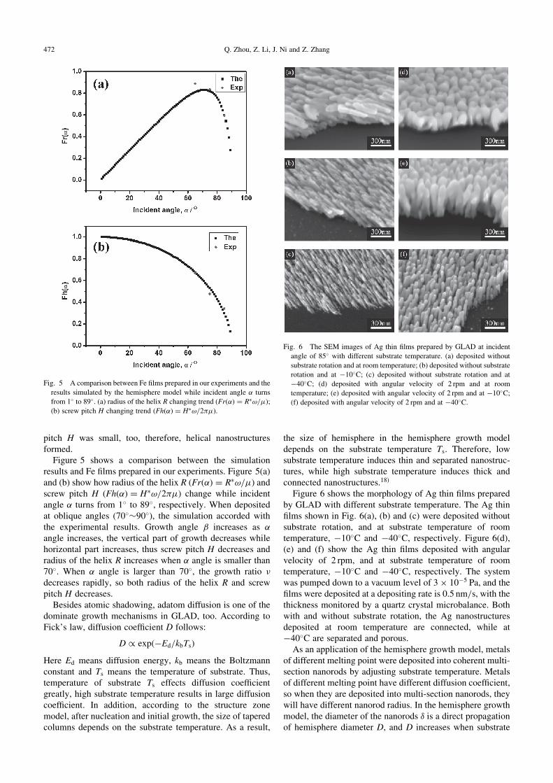
Figure 5 shows a comparison between the simulationresults and Fe films prepared in our experiments. Figure 5(a)and (b) show how radius of the helix R (Frð�Þ ¼ R�!=) andscrew pitch H (Fhð�Þ ¼ H�!=2�) change while incidentangle � turns from 1� to 89�, respectively. When depositedat oblique angles (70��90�), the simulation accorded withthe experimental results. Growth angle � increases as �angle increases, the vertical part of growth decreases whilehorizontal part increases, thus screw pitch H decreases andradius of the helix R increases when � angle is smaller than70�. When � angle is larger than 70�, the growth ratio decreases rapidly, so both radius of the helix R and screwpitch H decreases.
Besides atomic shadowing, adatom diffusion is one of thedominate growth mechanisms in GLAD, too. According toFick’s law, diffusion coefficient D follows:
D / expð�Ed=kbTsÞ
Here Ed means diffusion energy, kb means the Boltzmannconstant and Ts means the temperature of substrate. Thus,temperature of substrate Ts effects diffusion coefficientgreatly, high substrate temperature results in large diffusioncoefficient. In addition, according to the structure zonemodel, after nucleation and initial growth, the size of taperedcolumns depends on the substrate temperature. As a result,
the size of hemisphere in the hemisphere growth modeldepends on the substrate temperature Ts. Therefore, lowsubstrate temperature induces thin and separated nanostruc-tures, while high substrate temperature induces thick andconnected nanostructures.18)
Figure 6 shows the morphology of Ag thin films preparedby GLAD with different substrate temperature. The Ag thinfilms shown in Fig. 6(a), (b) and (c) were deposited withoutsubstrate rotation, and at substrate temperature of roomtemperature, �10�C and �40�C, respectively. Figure 6(d),(e) and (f) show the Ag thin films deposited with angularvelocity of 2 rpm, and at substrate temperature of roomtemperature, �10�C and �40�C, respectively. The systemwas pumped down to a vacuum level of 3� 10�5 Pa, and thefilms were deposited at a depositing rate is 0.5 nm/s, with thethickness monitored by a quartz crystal microbalance. Bothwith and without substrate rotation, the Ag nanostructuresdeposited at room temperature are connected, while at�40�C are separated and porous.
As an application of the hemisphere growth model, metalsof different melting point were deposited into coherent multi-section nanorods by adjusting substrate temperature. Metalsof different melting point have different diffusion coefficient,so when they are deposited into multi-section nanorods, theywill have different nanorod radius. In the hemisphere growthmodel, the diameter of the nanorods � is a direct propagationof hemisphere diameter D, and D increases when substrate
Fig. 6 The SEM images of Ag thin films prepared by GLAD at incident
angle of 85� with different substrate temperature. (a) deposited without
substrate rotation and at room temperature; (b) deposited without substrate
rotation and at �10�C; (c) deposited without substrate rotation and at
�40�C; (d) deposited with angular velocity of 2 rpm and at room
temperature; (e) deposited with angular velocity of 2 rpm and at �10�C;
(f) deposited with angular velocity of 2 rpm and at �40�C.
Fig. 5 A comparison between Fe films prepared in our experiments and the
results simulated by the hemisphere model while incident angle � turns
from 1� to 89�. (a) radius of the helix R changing trend (Frð�Þ ¼ R�!=);
(b) screw pitch H changing trend (Fhð�Þ ¼ H�!=2�).
472 Q. Zhou, Z. Li, J. Ni and Z. Zhang

temperature rises or melting point of material becomes lower.Thus in order to depositing coherent multi-section nanorodswith different melting point materials, one should deposithigh melting point material in high substrate temperature andlow melting point material in low temperature. Figure 7shows the Fe-Ag thin films prepared by GLAD with differentsubstrate temperature. We use liquid nitrogen to control thesubstrate temperature. Substrates and liquid nitrogen contain-er are connected with a copper belt, which transfers heat fromsubstrates to liquid nitrogen. A k style thermocouple is usedto measure the temperature of substrates. The Fe-Ag nano-structures in Fig. 7(a) were deposited at room temperature,
and the Fe (bulk melting point is 1535�C) nanorods areseparated but the Ag (bulk melting point is 960�C) nanorodsare connected to each other; the ones in Fig. 7(b) weredeposited at �40�C, and the Ag nanorods are separated butthe Fe nanorods become very thin that two or three Fe rodsconnect to one Ag rod; the nanostructures in Fig. 7(c) weredeposited at room temperature while depositing Fe and at�40�C while depositing Ag, and the multi-section nanorodsare coherent.
In summary, we have built a simple model which is calledhemisphere growth model to study the rule of glancing angledeposition. Influence of experiment conditions such asincidence angle, incidence rate, substrate temperature, andsubstrate rotation rate are theoretical analyzed and simulatedby the hemisphere growth model, and validated respectivelyby amount of experiment. As an application of the model,metals of different melting point were deposited intocoherent multi-section nanorods by adjusting substratetemperature. This study provides a simple way to realizethe rule of glancing angle deposition, and help to achievedifferent morphologies by adjusting experiment conditionsof GLAD.
Acknowledgments
The authors are grateful to the financial support by theNational Natural Science Foundation of China (50931002and 61076003), and the National Basic Research Program ofChina (973 program, 2007CB936601 and 2010CB731600).
REFERENCES
1) K. Robbie, L. J. Friedrich, S. K. Dew, T. Smy and M. J. Brett: J. Vac.
Sci. Technol. A 13 (1995) 1032–1035.
2) K. Robbie and M. J. Brett: J. Vac. Sci. Technol. A 15 (1997) 1460–
1465.
3) Matthew M. Hawkeye and Michael J. Brett: J. Vac. Sci. Technol. A 25
(2007) 1317–1335.
4) Cristina Buzea, a Kate Kaminska, Gisia Beydaghyan, Tim Brown,
Chelsea Elliott, Cory Dean and Kevin Robbie: J. Vac. Sci. Technol. B
23 (2005) 2545–2552.
5) H. T. G. Hentzell, C. R. M. Grovenor and D. A. Smith: J. Vac. Sci.
Technol. A 2 (1984) 218–219.
6) M. Malac, R. F. Egerton, M. J. Brett and B. Dick: J. Vac. Sci. Technol.
B 17 (1999) 2671.
7) M. Malac and R. F. Egerton: J. Vac. Sci. Technol. A 19 (2001) 158.
8) B. Dick and M. J. Brett: J. Vac. Sci. Technol. B 21 (2003) 23.
9) S. R. Kennedy, M. J. Brett, H. Miguez, O. Toader and S. John:
Photonics Nanostructures 1 (2003) 37.
10) B. Dick, M. J. Brett, T. J. Smy, M. R. Freeman, M. Malac and R. F.
Egerton: J. Vac. Sci. Technol. A 18 (2000) 1838.
11) H. Alouach, H. Fujiwara and G. J. Mankey: J. Vac. Sci. Technol. A 23
(2005) 1046.
12) J. P. Singh, F. Tang, T. Karabacak, T. M. Lu and G. C. Wang: J. Vac.
Sci. Technol. B 22 (2004) 1048.
13) A. Lakhtakia: Mater. Sci. Eng. C 19 (2002) 427.
14) M. M. HawKeye and M. J. Brett: J. Vac. Sci. Technol. A 25 (2007)
1317.
15) Ralph A. Tripp, Richard A. Dluhy and Yiping Zhao: Nanotoday 3
(2008) 31–37.
16) S. B. Chaney, S. Shanmukh, R. A. Dluhy and Y.-P. Zhao: Appl. Phys.
Lett. 87 (2005) 031908.
17) N. Jie, Z. Yu, Z. Qin and Z. Zhengjun: J. Am. Ceram. Soc. 91 (2008)
(10) 3458–3460.
18) C. M. Zhou and D. Gall: J. Vac. Sci. Technol. A 25 (2007) 312–318.
Fig. 7 The SEM images of Fe-Ag thin films prepared by GLAD with
different substrate temperature. (a) deposited at room temperature; (b)
deposited at�40�C; (c) deposit Fe at room temperature and Ag at�40�C.
A Simple Model to Describe the Rule of Glancing Angle Deposition 473


![Promote. engage. Collaborate. JANUARY 2015 Glancing ......Promote. engage. Collaborate. [ JANUARY 2015 ] (218) 732-4111 Glancing Back At 2014 & Forward Into 2015 in this issue •](https://img.dokumen.tips/doc/110x75/6037f0ce6f2d00546d3dee64/promote-engage-collaborate-january-2015-glancing-promote-engage-collaborate.jpg)