Embed Size (px)
Citation preview
A. Silver
1
Superconductor Technologies for
Extreme Computing
Arnold Silver
Workshop on Frontiers of Extreme Computing
Monday, October 24, 2005
Santa Cruz, CA
A. Silver
2
Outline Introduction
Single Flux Quantum (SFQ) Technology
State-of-the-Art
Prospects
Quantum Computing
Summary
A. Silver
3
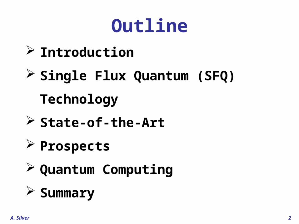
Notional Diagram of a Superconductor Processor
Superconductor processors communicate with local cryogenic RAM and with the cryogenic switch network.
Cryogenic RAM communicates via wideband I/O with ambient electronics.
Superconductor Processors
Cryogenic RAM
High Speed Cryogenic Switch Network
Ambient Electronics
Wideband I/O
4 Kelvin
Introduction

A. Silver
4
Early Technology Limited Early superconductor logic was voltage-latching
– Voltage state data– AC power required– Speed limited by RC load and reset time (~GHz)
Single Flux Quantum (SFQ) is latest generation.– Current/Flux state data– SFQ pulses transfer data– DC powered– Higher speed (~100 GHz)
Incremental progress on DoD contracts. – Small annual budgets – Focus on small circuit demos– Minimal infrastructure investment
Introduction
A. Silver
5
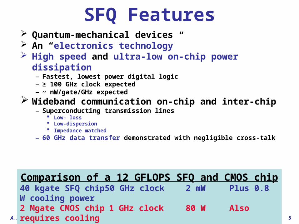
SFQ Features Quantum-mechanical devices An “electronics technology” High speed and ultra-low on-chip power dissipation
– Fastest, lowest power digital logic– ≥ 100 GHz clock expected– ~ nW/gate/GHz expected
Wideband communication on-chip and inter-chip– Superconducting transmission lines
Low- loss Low-dispersion Impedance matched
– 60 GHz data transfer demonstrated with negligible cross-talk
Introduction
Comparison of a 12 GFLOPS SFQ and CMOS chip40 kgate SFQ chip 50 GHz clock 2 mW Plus 0.8 W cooling power2 Mgate CMOS chip 1 GHz clock 80 W Also requires cooling

A. Silver
6
Some Issues Need To Be Addressed Present disadvantages
– Low chip density and production maturity– Inadequate cryogenic RAM– Cryogenic cooling– Cryogenic - ambient I/O
Density and maturity will increase with better VLSI Promising candidates for cryogenic RAM
– Hybrid superconductor-CMOS– Hybrid superconductor-MRAM– SFQ RAM
Cryogenics is an enabler for low power Options for wideband I/O exist
Introduction
A. Silver
7
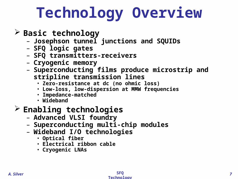
Technology Overview Basic technology
– Josephson tunnel junctions and SQUIDs– SFQ logic gates– SFQ transmitters-receivers– Cryogenic memory– Superconducting films produce microstrip and stripline transmission
lines• Zero-resistance at dc (no ohmic loss)• Low-loss, low-dispersion at MMW frequencies• Impedance-matched• Wideband
Enabling technologies– Advanced VLSI foundry– Superconducting multi-chip modules– Wideband I/O technologies
• Optical fiber• Electrical ribbon cable• Cryogenic LNAs
SFQ Technology
A. Silver
8
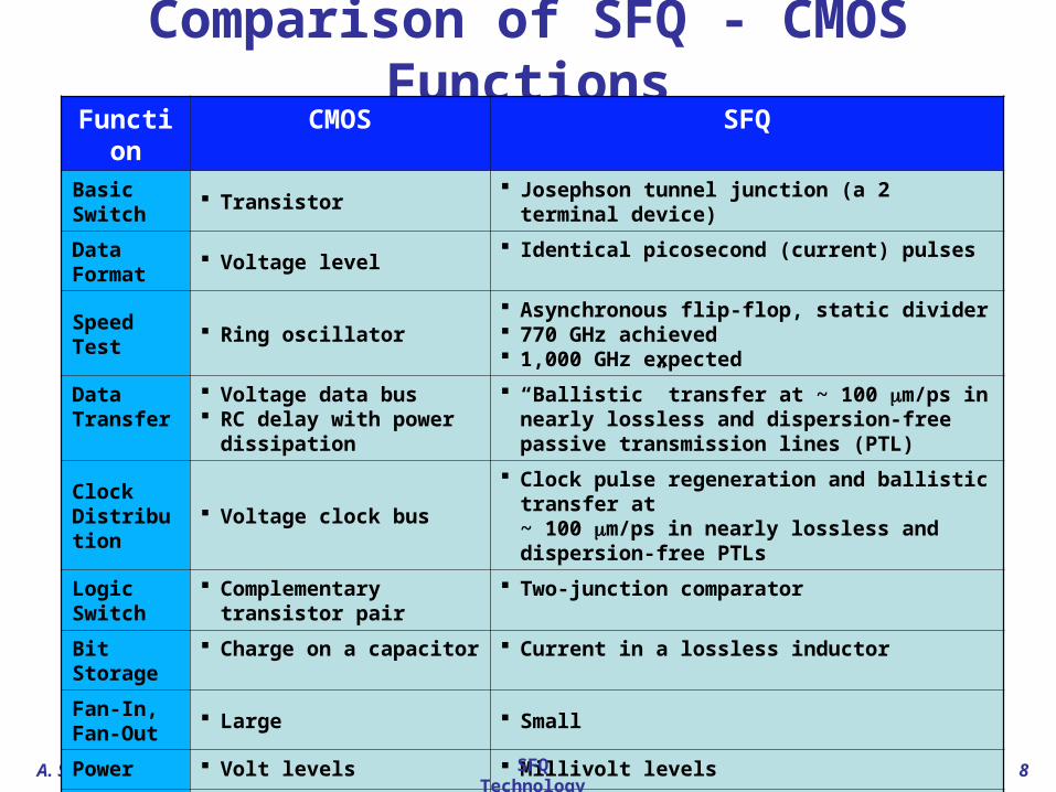
Comparison of SFQ - CMOS FunctionsFunction CMOS SFQ
Basic Switch Transistor Josephson tunnel junction (a 2 terminal device)
Data Format Voltage level Identical picosecond (current) pulses
Speed Test Ring oscillator Asynchronous flip-flop, static divider 770 GHz achieved 1,000 GHz expected
Data Transfer
Voltage data bus RC delay with power
dissipation
“Ballistic” transfer at ~ 100 m/ps in nearly lossless and dispersion-free passive transmission lines (PTL)
Clock Distribution
Voltage clock bus Clock pulse regeneration and ballistic transfer at
~ 100 m/ps in nearly lossless and dispersion-free PTLs
Logic Switch Complementary transistor pair Two-junction comparator
Bit Storage Charge on a capacitor Current in a lossless inductor
Fan-In, Fan-Out
Large Small
Power Volt levels Millivolt levels
Power Distribution
Ohmic power bus Lossless superconducting wiring
Noise ≥ 300 K thermal noise 4 K thermal noise that enables low power operation
SFQ Technology
A. Silver
9
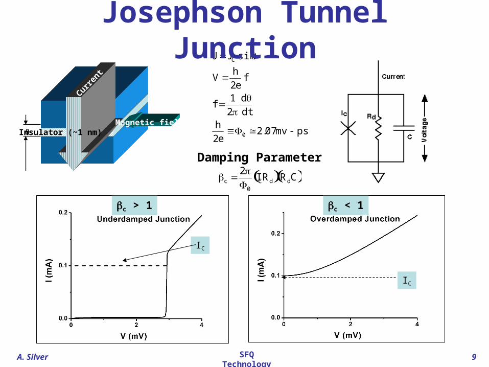
Current
Insulator (~1 nm)Magnetic field
J JC sin
V h
2ef
f 12
ddt
h
2e0 2.07mv ps
Josephson Tunnel Junction
IC
c > 1
IC
c < 1
Damping Parameter
c 20
ICRd RdC
SFQ Technology
A. Silver
10
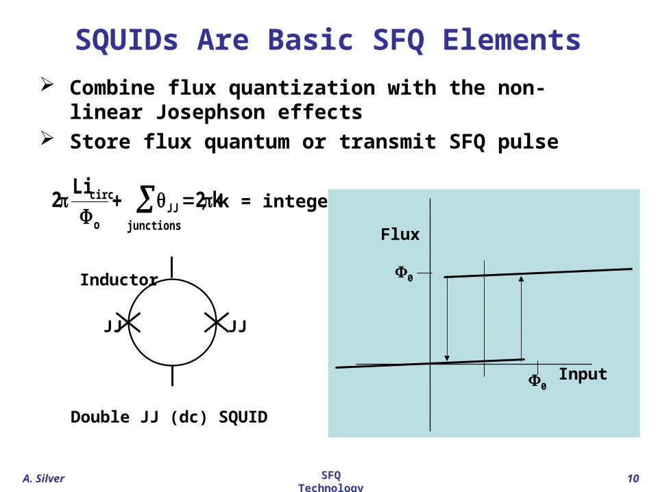
SQUIDs Are Basic SFQ Elements
Combine flux quantization with the non-linear Josephson effects
Store flux quantum or transmit SFQ pulse
2Licirco
JJjunctions
2k ; k = integer
Double JJ (dc) SQUID
JJ JJ
Inductor
Input
Flux
0
0
SFQ Technology
A. Silver
11
SFQ Is A Current Based Technology
When (Input + Ibias) exceeds JJ critical current Ic, JJ “flips”, producing an SFQ pulse.
Area of the pulse is 0=2.067 mV-ps Pulse width shrinks as JC increases SFQ logic is based on counting
single flux quanta
SFQ pulses propagate along impedance-matched passive transmission line (PTL) at the speed of light in the line (~ c/3).
Multiple pulses can propagate in PTL simultaneously in both directions.
Input
~1mV
~2ps
Ibias
JJ
SFQ Technology
A. Silver
12
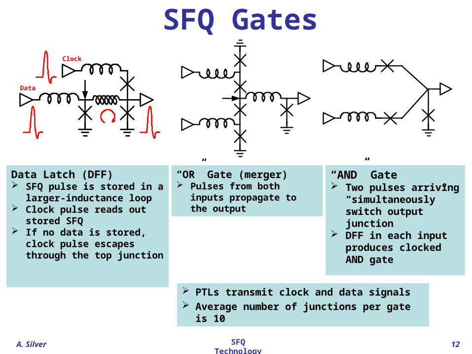
SFQ Gates
Data Latch (DFF) SFQ pulse is stored in a
larger-inductance loop Clock pulse reads out stored
SFQ If no data is stored, clock
pulse escapes through the top junction
Clock
Data
“OR” Gate (merger) Pulses from both inputs
propagate to the output
“AND” Gate Two pulses arriving
“simultaneously” switch output junction
DFF in each input produces clocked AND gate
PTLs transmit clock and data signals Average number of junctions per gate is 10
SFQ Technology
A. Silver
13
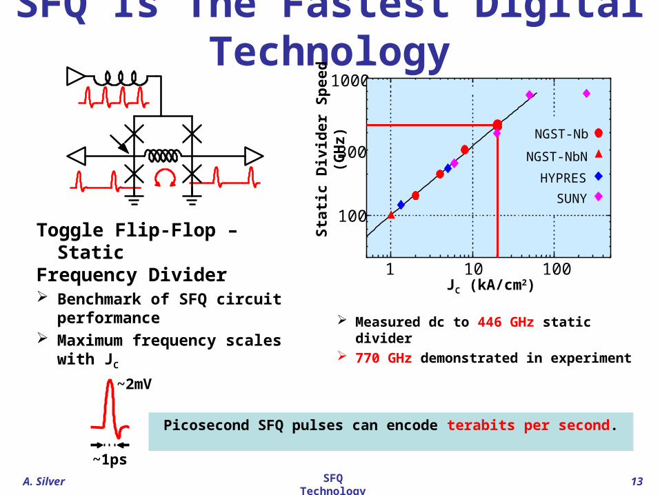
SFQ Is The Fastest Digital Technology
Toggle Flip-Flop – Static Frequency Divider Benchmark of SFQ circuit
performance Maximum frequency scales with JC
Measured dc to 446 GHz static divider 770 GHz demonstrated in experiment
Picosecond SFQ pulses can encode terabits per second.
~1ps
~2mV
SFQ Technology
Sta
tic
Div
ider
Sp
eed
(G
Hz)
JC (kA/cm2)
100
1000
1 10 100
300NGST-Nb
NGST-NbN
HYPRES
SUNY
A. Silver
14
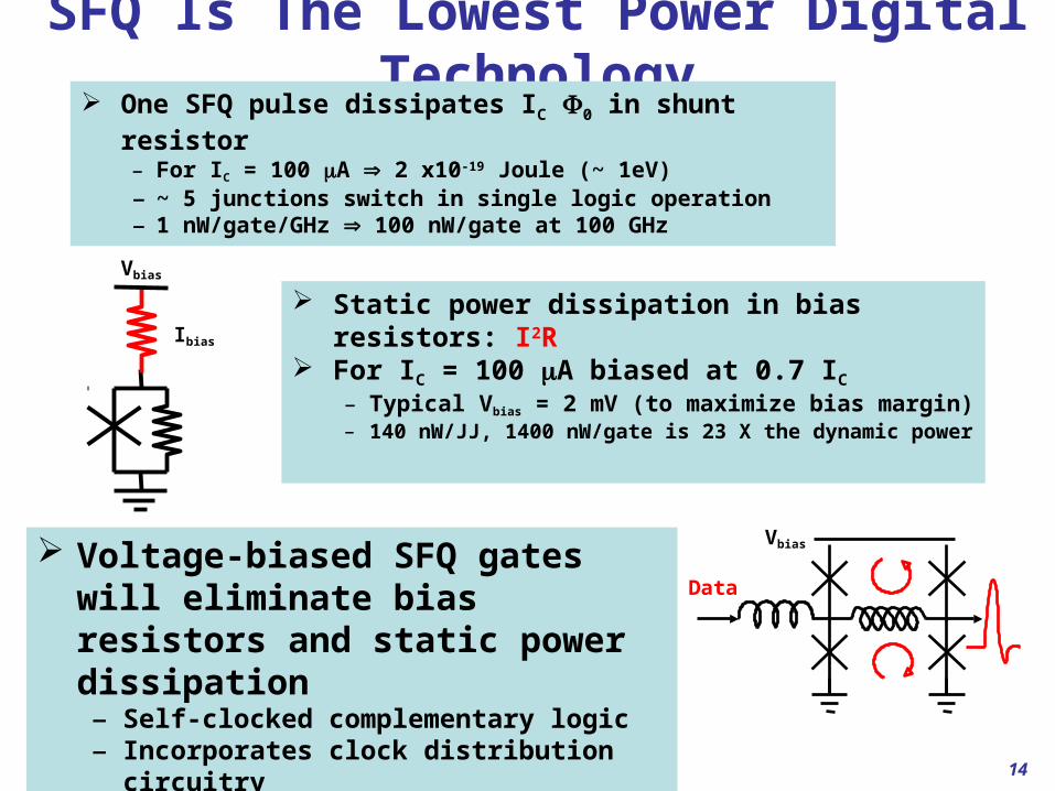
SFQ Is The Lowest Power Digital Technology One SFQ pulse dissipates IC 0 in shunt resistor
– For IC = 100 A 2 x10-19 Joule (~ 1eV)– ~ 5 junctions switch in single logic operation– 1 nW/gate/GHz 100 nW/gate at 100 GHz
SFQ Technology
Static power dissipation in bias resistors: I2R For IC = 100 A biased at 0.7 IC
– Typical Vbias = 2 mV (to maximize bias margin)– 140 nW/JJ, 1400 nW/gate is 23 X the dynamic power
Vbias
Ibias
Data
Vbias Voltage-biased SFQ gates will eliminate bias resistors and static power dissipation– Self-clocked complementary logic– Incorporates clock distribution circuitry– Vbias = 0FClock
A. Silver
15
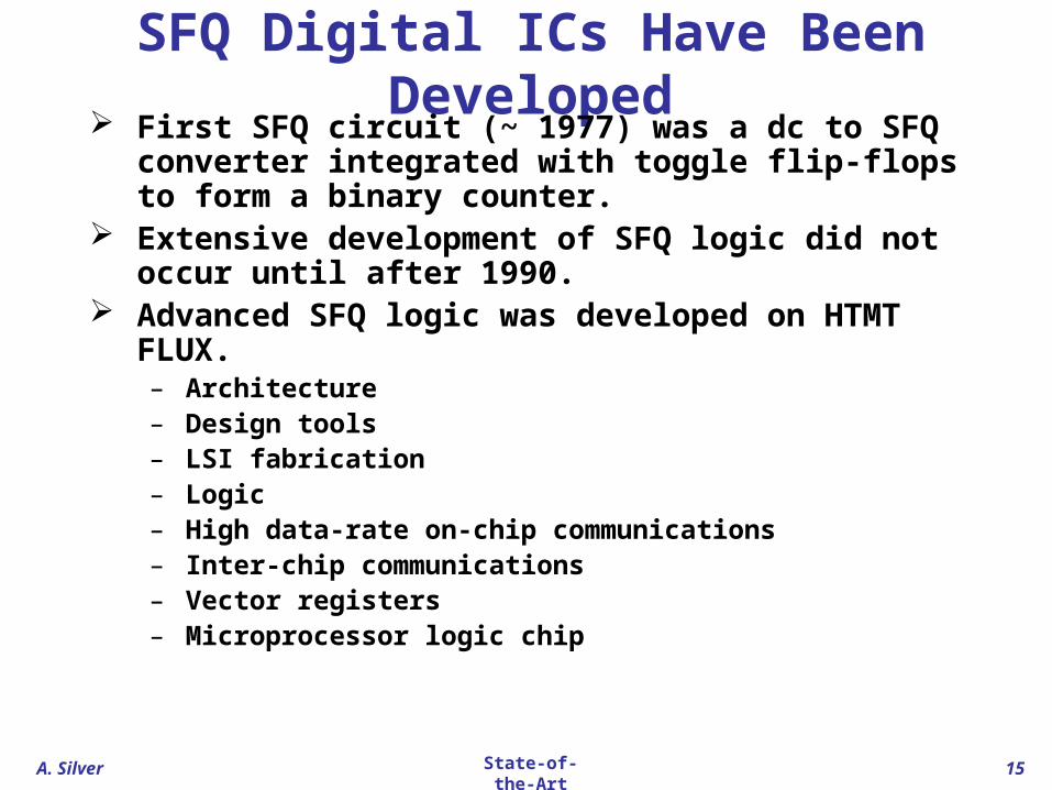
SFQ Digital ICs Have Been Developed First SFQ circuit (~ 1977) was a dc to SFQ converter
integrated with toggle flip-flops to form a binary counter. Extensive development of SFQ logic did not occur until
after 1990. Advanced SFQ logic was developed on HTMT FLUX.
– Architecture– Design tools– LSI fabrication– Logic– High data-rate on-chip communications– Inter-chip communications– Vector registers– Microprocessor logic chip
State-of-the-Art
A. Silver
16
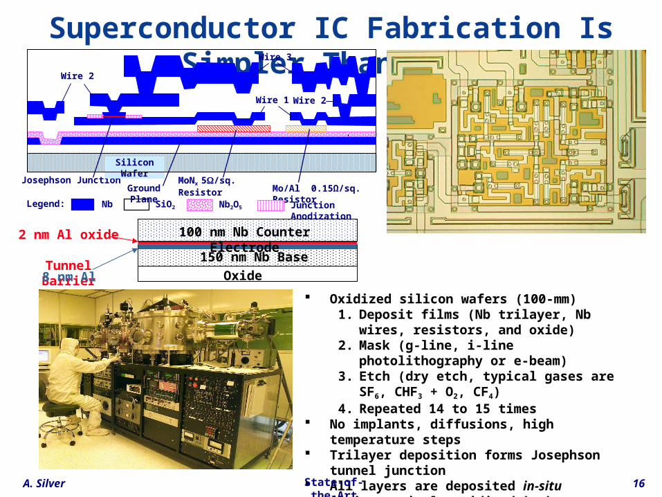
Superconductor IC Fabrication Is Simpler Than CMOS
Oxidized silicon wafers (100-mm)1. Deposit films (Nb trilayer, Nb wires, resistors, and oxide)2. Mask (g-line, i-line photolithography or e-beam)3. Etch (dry etch, typical gases are SF6, CHF3 + O2, CF4)4. Repeated 14 to 15 times
No implants, diffusions, high temperature steps Trilayer deposition forms Josephson tunnel junction All layers are deposited in-situ Al is passively oxidized in-situ at room temperature 1 m minimum feature, 2.6 m wire pitch Throughput limited by deposition tools
State-of-the-Art
2 nm Al oxide Tunnel Barrier
8 nm Al
150 nm Nb Base Electrode
Oxide
100 nm Nb Counter Electrode
Legend:
Josephson Junction
Nb2O5SiO2
MoNx 5/sq. Resistor
Nb
Mo/Al 0.15Ω/sq. Resistor
Junction Anodization
Silicon Wafer
Wire 1
Wire 2
Wire 3
Ground Plane
Wire 2
A. Silver
17
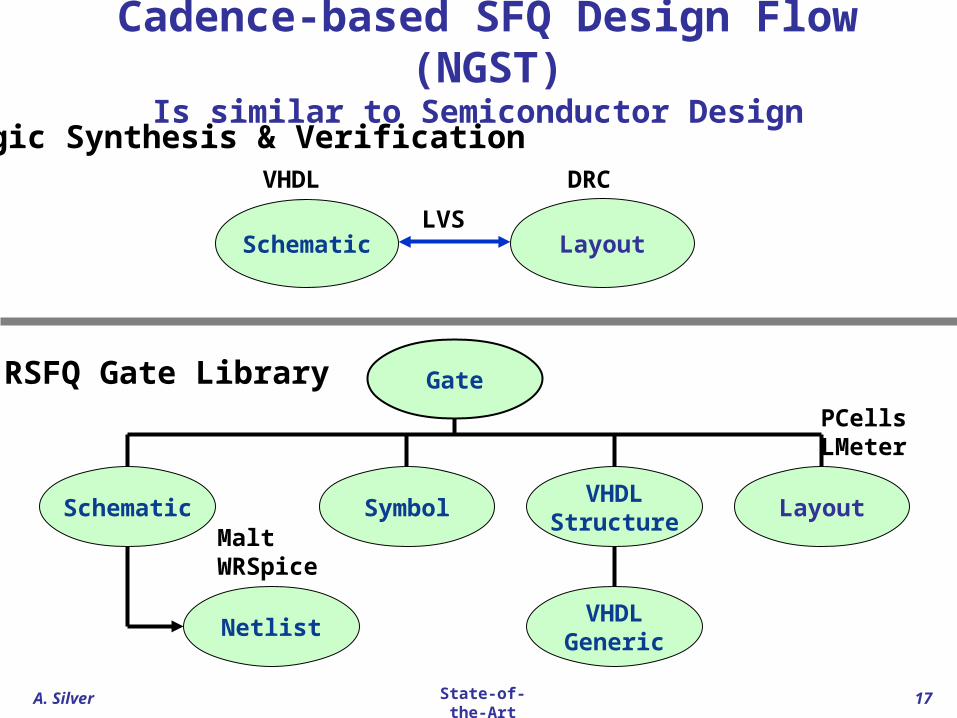
Cadence-based SFQ Design Flow (NGST)Is similar to Semiconductor Design
Schematic Layout
DRC
LVS
VHDL
RSFQ Gate Library
Logic Synthesis & Verification
SymbolVHDL
StructureSchematic Layout
Netlist
PCellsLMeter
MaltWRSpice
Gate
VHDLGeneric
State-of-the-Art

A. Silver
18
Complex Chips Have Been Reported
Function Complexity Speed Cell Library Organizations
FLUX-1. 8-bit Pprototype.25 30-bit-dual-opinstructions.
63 K Junctions.10.3 mm x 10.6 mm.
Designed for 20 GHz.Not tested.
Yes.Incorporatesdrivers/receivers forPTL.
Northrop Grumman,Stony Brook, JPL
CORE110.8-bit bit-serial P.7 8-bit instructions.
7 K Junctions.3.4 mm x 3.2 mm.
21 GHz local clock.1 GHz system clock.Fully functional.
Yes.Gates connected byJTLs and/or PTLs
ISTEC-SRL,Nagoya U.,
Yokohama National U.
MAC and Prefilter forprogrammable pass-band A/D converter.
6 K–11 K Junctions.5 mm x 5 mm.
20 GHz design
Yes.Gates connected byparameterized JTLsand/or PTLs
Northrop Grumman
A/D converter 6 K Junctions. 19.6 GHz. ? Hypres
Digital receiver 12 K Junctions. 12 GHz. ? Hypres
FIFO buffer memory4K bit.2.6 mm x 2.5 mm
32 bits tested at40 G Hz.
No Northrop Grumman
X-bar switch128 x 128 switch.32 x 32 module.
2.5 Gbps. NoNSA, Northrop
Grumman
SFQ X-bar switch 32 x 32 module. 40 Gbps. No Northrop Grumman
State-of-the-Art
A. Silver
19
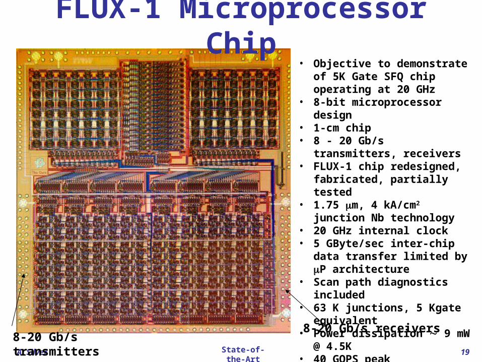
FLUX-1 Microprocessor Chip• Objective to demonstrate of 5K Gate
SFQ chip operating at 20 GHz• 8-bit microprocessor design• 1-cm chip• 8 - 20 Gb/s transmitters, receivers• FLUX-1 chip redesigned, fabricated,
partially tested• 1.75 m, 4 kA/cm2 junction Nb
technology• 20 GHz internal clock• 5 GByte/sec inter-chip data transfer
limited by P architecture• Scan path diagnostics included• 63 K junctions, 5 Kgate equivalent • Power dissipation 9 mW @ 4.5K• 40 GOPS peak computational
capability (8-bits @ 20-GHz clock)• Fabricated in TRW 4 kA/cm2 process
in 2002
8-20 Gb/s receivers8-20 Gb/s transmitters
State-of-the-Art
A. Silver
20
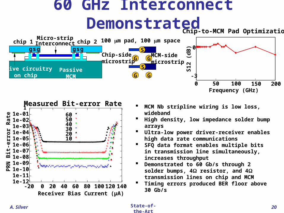
60 GHz Interconnect Demonstrated
MCM Nb stripline wiring is low loss, wideband High density, low impedance solder bump arrays Ultra-low power driver-receiver enables high data
rate communications SFQ data format enables multiple bits in
transmission line simultaneously, increases throughput
Demonstrated to 60 Gb/s through 2 solder bumps, 4 resistor, and 4 transmission lines on chip and MCM
Timing errors produced BER floor above 30 Gb/s
Chip-to-MCM Pad Optimization
-3
0
0 50 100 150 200Frequency (GHz)
S12
(dB
)
Passive MCM
chip 1
Active circuitryon chip
Micro-stripInterconnect
sg gsg gchip 2 100 m pad, 100 m space
S
G G
GG
SChip-sidemicrostrip
MCM-sidemicrostrip
11e-011e-021e-031e-041e-051e-061e-071e-081e-091e-101e-111e-12
-20 0 20 40 60 80 100 120 140
PRN
Bit-
erro
r Rat
e
Receiver Bias Current (µA)
605040302010
Measured Bit-error Rate
State-of-the-Art
A. Silver
21
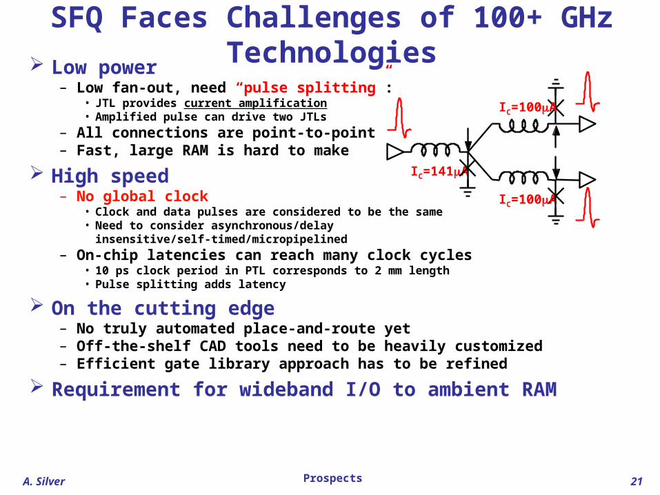
Low power– Low fan-out, need “pulse splitting”:
• JTL provides current amplification• Amplified pulse can drive two JTLs
– All connections are point-to-point– Fast, large RAM is hard to make
High speed– No global clock
• Clock and data pulses are considered to be the same• Need to consider asynchronous/delay insensitive/self-timed/micropipelined
– On-chip latencies can reach many clock cycles• 10 ps clock period in PTL corresponds to 2 mm length• Pulse splitting adds latency
On the cutting edge– No truly automated place-and-route yet– Off-the-shelf CAD tools need to be heavily customized– Efficient gate library approach has to be refined
Requirement for wideband I/O to ambient RAM
SFQ Faces Challenges of 100+ GHz Technologies
IC=141A
IC=100A
IC=100A
Prospects
A. Silver
22
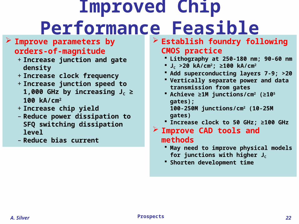
Improved Chip Performance Feasible Improve parameters by orders-
of-magnitude + Increase junction and gate density+ Increase clock frequency+ Increase junction speed to 1,000
GHz by increasing JC ≥ 100 kA/cm2
+ Increase chip yield– Reduce power dissipation to SFQ
switching dissipation level– Reduce bias current
Establish foundry following CMOS practice Lithography at 250-180 nm; 90-60 nm JC >20 kA/cm2; ≥100 kA/cm2
Add superconducting layers 7-9; >20 Vertically separate power and data
transmission from gates Achieve ≥1M junctions/cm2 (≥105 gates);
100-250M junctions/cm2 (10-25M gates) Increase clock to 50 GHz; ≥100 GHz
Improve CAD tools and methods May need to improve physical models for
junctions with higher JC
Shorten development time
Prospects
A. Silver
23
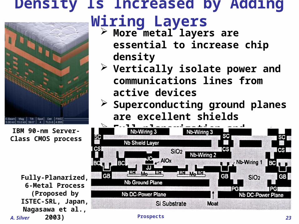
Density Is Increased by Adding Wiring Layers
Fully-Planarized, 6-Metal Process (Proposed by
ISTEC-SRL, Japan, Nagasawa et al., 2003)
IBM 90-nm Server-Class CMOS process
Prospects
More metal layers are essential to increase chip density
Vertically isolate power and communications lines from active devices
Superconducting ground planes are excellent shields
Full planarization and competitive lithography
A. Silver
24
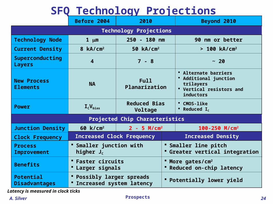
SFQ Technology Projections Before 2004 2010 Beyond 2010
Technology Projections
Technology Node 1 m 250 - 180 nm 90 nm or better
Current Density 8 kA/cm2 50 kA/cm2 > 100 kA/cm2
Superconducting Layers 4 7 - 8 ~ 20
New Process Elements NA Full Planarization Alternate barriers Additional junction trilayers Vertical resistors and inductors
Power ICVbias Reduced Bias Voltage CMOS-like Reduced IC
Projected Chip Characteristics
Junction Density 60 k/cm2 2 - 5 M/cm2 100-250 M/cm2
Clock Frequency < 20 GHz 50 - 100 GHz 100 - 250 GHz
Power 0.2 W/Junction 8 nW/GHz/Junction 0.4 nW/GHz/Junction
Prospects
Increased Clock Frequency Increased Density
Process Improvement Smaller junction with higher JC
Smaller line pitch Greater vertical integration
Benefits Faster circuits Larger signals
More gates/cm2
Reduced on-chip latency
Potential Disadvantages Possibly larger spreads Increased system latency
Potentially lower yield
Latency is measured in clock ticks
A. Silver
25
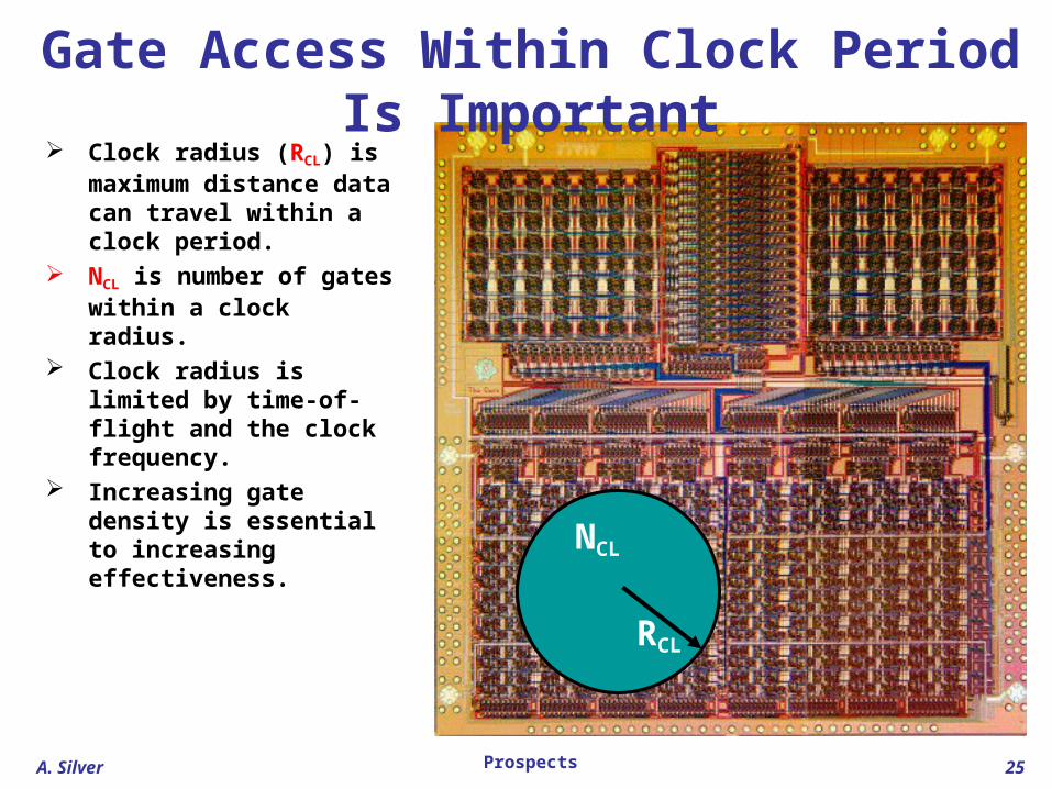
Gate Access Within Clock Period Is Important Clock radius (RCL) is
maximum distance data can travel within a clock period.
NCL is number of gates within a clock radius.
Clock radius is limited by time-of-flight and the clock frequency.
Increasing gate density is essential to increasing effectiveness.
RCL
NCL
Prospects
A. Silver
26
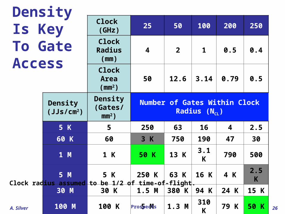
Density Is Key To Gate Access
Clock (GHz)
25 50 100 200 250
Clock Radius(mm)
4 2 1 0.5 0.4
Clock Area(mm2)
50 12.6 3.14 0.79 0.5
Density (JJs/cm2)
Density(Gates/mm2)
Number of Gates Within Clock Radius (NCL)
5 K 5 250 63 16 4 2.5
60 K 60 3 K 750 190 47 30
1 M 1 K 50 K 13 K 3.1 K 790 500
5 M 5 K 250 K 63 K 16 K 4 K 2.5 K
30 M 30 K 1.5 M 380 K 94 K 24 K 15 K
100 M 100 K 5 M 1.3 M 310 K 79 K 50 K
250 M 250 K 12.5 M 3.1 M 790 K 200 K 130 K
Clock radius assumed to be 1/2 of time-of-flight.
Prospects
A. Silver
27
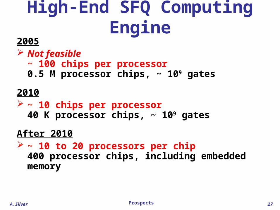
High-End SFQ Computing Engine2005 Not feasible
~ 100 chips per processor 0.5 M processor chips, ~ 109 gates
2010 ~ 10 chips per processor
40 K processor chips, ~ 109 gates
After 2010 ~ 10 to 20 processors per chip
400 processor chips, including embedded memory
Prospects
A. Silver
28
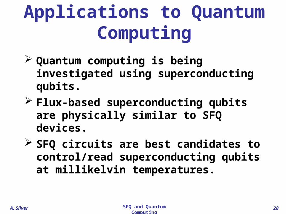
Applications to Quantum Computing
Quantum computing is being investigated using superconducting qubits.
Flux-based superconducting qubits are physically similar to SFQ devices.
SFQ circuits are best candidates to control/read superconducting qubits at millikelvin temperatures.
SFQ and Quantum Computing
A. Silver
29
SFQ needs major engineering development in chip technology if it is going to be a player in high-end computing.
The engineering requirements are understood and a development plan defined.
Prospects are exciting and achievable.
Summary
Summary