Embed Size (px)
Citation preview
applied sciences
Article
A Self-Testing Platform with a Foreground DigitalCalibration Technique for SAR ADCs
Yi-Hsiang Juan 1, Hong-Yi Huang 2, Shuenn-Yuh Lee 1, Shin-Chi Lai 3, Wen-Ho Juang 1
and Ching-Hsing Luo 1,*1 The Department of Electrical Engineering, National Cheng Kung University, Tainan 701, Taiwan;
[email protected] (Y.-H.J.); [email protected] (S.-Y.L.); [email protected] (W.-H.J.)2 The Department of Electrical Engineering, National Taipei University, Taipei, 23741, Taiwan;
[email protected] The Department of Computer Science and Information Engineering, Nanhua University, Chiayi 62249,
Taiwan; [email protected]* Correspondence: [email protected]; Tel.: +886-6-2757575-62375; Fax: +886-6-234-548
Academic Editor: Teen-Hang MeenReceived: 29 May 2016; Accepted: 26 July 2016; Published: 29 July 2016
Abstract: This study presents a self-testing platform with a foreground digital calibration techniquefor successive approximation register (SAR) analog-to-digital converters (ADCs). A high-accuracydigital-to-analog converter (DAC) with digital control is used for the proposed self-testing platformto generate the sinusoidal test signal. This signal is then implemented using an Arduino board, andthe clock signal is generated to test the ADCs. In addition, fast Fourier transform and recursivediscrete Fourier transform (RDFT) processors are adopted for dynamic performance evaluationand calibration of the ADCs. The third harmonic distortion caused by the non-linearity of thetrack-and-hold circuit, the mismatch of the DAC capacitor array, and the direct current (DC)offset of the comparator can be calculated using the processors to improve the ADC performance.The advantages of the proposed platform include its low cost, high integration, and no need for anextra analogy compensation circuit to deal with calibration. In this work a 12 bit SAR ADC and anRDFT processor are used in the Taiwan Semiconductor Manufacturing Co., Ltd. (TSMC) 0.18 µmstandard complementary metal–oxide–semiconductor (CMOS) process with a sampling rate of 18.75kS/s to validate the proposed method. The measurement results show that the signal-to-noise anddistortion ratio is 55.07 dB before calibration and 61.35 dB after calibration.
Keywords: analog-to-digital converters (ADCs); digital calibration method; self-testing; successiveapproximation register ADC (SAR)
1. Introduction
An analog-to-digital converter (ADC) is an important component in various areas, such ascommunication and biomedical systems, among others. The performance limitations of the ADCsare mainly dominated by the static and dynamic non-linearity effects, which cause the harmonicdistortion in the output power spectrum. These non-linearities slightly deteriorate the overall systemperformance, and also increase the sensitivity to the process variation and system interface noisebecause of the technology scaling into the nano-scale region. A calibration method is thus essential toensure system quality [1,2]. The successive approximation register (SAR) analog-to-digital converter(ADC) has the advantages of medium speed conversion and medium to high resolution. It is thereforevery suitable for biomedical and communication systems. With regard to the implementation of mostSAR ADCs, the performance should be maintained by the internal circuits, including the track-and-hold(T/H) circuit, the DAC capacitor array, and the comparator circuit. However, the non-linearity of
Appl. Sci. 2016, 6, 217; doi:10.3390/app6080217 www.mdpi.com/journal/applsci
Appl. Sci. 2016, 6, 217 2 of 13
the internal circuits always limits the performance of the ADCs. This is the reason why a calibrationmethod is required to overcome this problem. In this paper we focus on the digital calibration method.For example, the lookup table or the state-space technique is a common calibration method for ADCerror correction [3]. The correction in this approach is based on a table that uses pre-calculated valuesor the slope of the input signal. However, the drawback of this method is the requirement of a largememory size, thus consuming more areas. An equalization-based digitally calibrated method isproposed in Reference [4]. The advantage of this is the reduction of both the ADC testing time and theconvergence time. In addition, this paper utilizes the least mean squares (LMS) algorithm to correctand calibrate the ADC error, similar to that in Reference [5].
An internal redundancy dithering (IRD) technique is reported in Reference [6]. The IRD methodbased on bit-weight calibration employs a pseudorandom bit sequence to determine the thresholdvalues. The method utilizes the LMS algorithm to calibrate the SAR ADC error. However, the maindrawback of the approaches in References [5,6] is that a high resolution ADC is required, which isimpractical in actual implementation. A fast-Fourier transform (FFT)-based calibration method forpipelined ADC is reported to calibrate the capacitor mismatch and non-linearity error of the operationalamplifier (OPAMP) [7]. However, the shortcoming of the FFT process is the consumption of morepower because all frequency bins should be computed during the operation mode. Juan et al. proposedan RDFT-based calibration algorithm to overcome this problem [8], because the RDFT processor hasthe advantages of variable transform length, lower complexity, and less hardware cost.
In this paper, we present a self-testing platform based on previous works [7,8] to measure theADC performance using the proposed testing stimulus and compensate for the error using a simplifieddigital calibration algorithm. A 12 bit SAR ADC and an RDFT processor are implemented in theTSMC 0.18 µm to verify the proposed platform. The output is analyzed using MATLAB (version7.6.0.324 (R2008a), The MathWorks, Natick, MA, USA, 2008), including the performance calculationand ADC calibration.
2. Proposed Self-Test Platform
2.1. Conventional SAR ADC Architecture
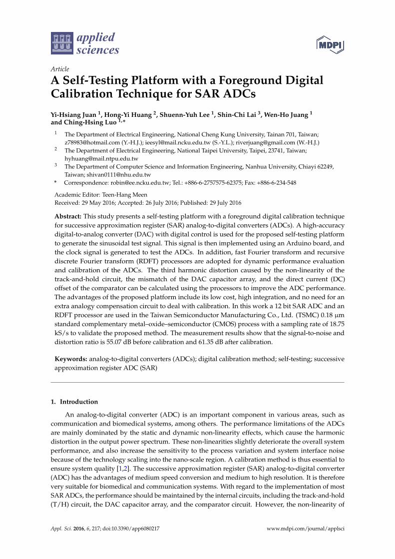
The basic block of the traditional SAR ADC includes a track-and-hold circuit (T/H), an N-bitDAC capacitor array, a comparator circuit, and a SAR controller (Figure 1). The SAR ADC generallyuses a binary-weighted method to implement the circuit [9]. According to the results for the switchingcapacitor array, the digital output signal can be obtained as Logical High (“1”) or Logical Low (“0”). Inaddition, some biomedical applications require an adaptive resolution using a multi-switch operatedin 8 bit or 12 bit mode [9]. However, the non-linearity of the multi-switch in the T/H circuit will limitthe SAR ADC performance. The proposed calibration method also has the capability of eliminatingthe non-linearity and enhancing the performance of the multi-mode SAR ADC. Figure 2 depicts themulti-mode SAR ADC structure. In this, switch S2 is applied to control the two operation modes,namely the 8 bit and 12 bit modes. The bootstrapped switch is also adopted to provide a smallon-resistance with a constant value and better linearity.
Appl. Sci. 2016, 6, 217 3 of 13
Appl. Sci. 2016, 6, 217 2 of 13
comparator circuit. However, the non‐linearity of the internal circuits always limits the
performance of the ADCs. This is the reason why a calibration method is required to overcome this
problem. In this paper we focus on the digital calibration method. For example, the lookup table or
the state‐space technique is a common calibration method for ADC error correction [3]. The
correction in this approach is based on a table that uses pre‐calculated values or the slope of the
input signal. However, the drawback of this method is the requirement of a large memory size, thus
consuming more areas. An equalization‐based digitally calibrated method is proposed in Reference
[4]. The advantage of this is the reduction of both the ADC testing time and the convergence time.
In addition, this paper utilizes the least mean squares (LMS) algorithm to correct and calibrate the
ADC error, similar to that in Reference [5].
An internal redundancy dithering (IRD) technique is reported in Reference [6]. The IRD
method based on bit‐weight calibration employs a pseudorandom bit sequence to determine the
threshold values. The method utilizes the LMS algorithm to calibrate the SAR ADC error. However,
the main drawback of the approaches in References [5,6] is that a high resolution ADC is required,
which is impractical in actual implementation. A fast‐Fourier transform (FFT)‐based calibration
method for pipelined ADC is reported to calibrate the capacitor mismatch and non‐linearity error of
the operational amplifier (OPAMP) [7]. However, the shortcoming of the FFT process is the
consumption of more power because all frequency bins should be computed during the operation
mode. Juan et al. proposed an RDFT‐based calibration algorithm to overcome this problem [8],
because the RDFT processor has the advantages of variable transform length, lower complexity,
and less hardware cost.
In this paper, we present a self‐testing platform based on previous works [7,8] to measure the
ADC performance using the proposed testing stimulus and compensate for the error using a
simplified digital calibration algorithm. A 12 bit SAR ADC and an RDFT processor are
implemented in the TSMC 0.18 μm to verify the proposed platform. The output is analyzed using
MATLAB (version 7.6.0.324 (R2008a), The MathWorks, Natick, MA, USA, 2008), including the
performance calculation and ADC calibration.
2. Proposed Self‐Test Platform
2.1. Conventional SAR ADC Architecture
The basic block of the traditional SAR ADC includes a track‐and‐hold circuit (T/H), an N‐bit
DAC capacitor array, a comparator circuit, and a SAR controller (Figure 1). The SAR ADC generally
uses a binary‐weighted method to implement the circuit [9]. According to the results for the
switching capacitor array, the digital output signal can be obtained as Logical High (“1”) or Logical
Low (“0”). In addition, some biomedical applications require an adaptive resolution using a
multi‐switch operated in 8 bit or 12 bit mode [9]. However, the non‐linearity of the multi‐switch in
the T/H circuit will limit the SAR ADC performance. The proposed calibration method also has the
capability of eliminating the non‐linearity and enhancing the performance of the multi‐mode SAR
ADC. Figure 2 depicts the multi‐mode SAR ADC structure. In this, switch S2 is applied to control
the two operation modes, namely the 8 bit and 12 bit modes. The bootstrapped switch is also
adopted to provide a small on‐resistance with a constant value and better linearity.
Figure 1. Traditional successive approximation register (SAR) Analog-to-Digital converter(ADC) structure.
Appl. Sci. 2016, 6, 217 3 of 13
Figure 1. Traditional successive approximation register (SAR) Analog‐to‐Digital converter (ADC)
structure.
Figure 2. Multi‐mode SAR ADC structure.
2.2. Proposed Calibration Method
A previous work [8] derived the proposed calibration formula using the FFT and a cosine
wave input signal. The third harmonic distortion value a3 can be detected by an RDFT processor.
The error factor Δn can be further calculated for the calibration. In addition, the calibration code was
only used for the first‐time test to reduce the complexity. This calibration method can not only
compensate for the error caused by the capacitor mismatch and DC offset in the traditional ADC
but it can also be applied to calibrate the T/H circuit in the multi‐mode SAR ADC (Figure 2).
The main calibration equation can be written as follows:
n n3 os
1.69620log 1.696
2048
A Ca V
, (1)
where A is the amplitude of the cosine wave, Cn is the value of each capacitor ratio, Δn is the error
factor of each capacitor mismatch, and Vos is the DC offset. The DC offset voltage of the comparator
circuit can be expressed as:
22
2ov ovDos t
D2 2
WV VR LV V
WRL
, (2)
where Vov, W/L, and Vt are the overdrive voltage, transistor size, and threshold voltage of the
differential pair, respectively. According to Equation (2), the threshold voltage is a static offset,
which does not affect the dynamic performance of the ADC. Meanwhile, both the overdrive voltage
and transistor size will degrade the ADC performance. Some approaches have been used to
overcome this problem and improve the DC offset, such as reducing the overdrive voltage or
increasing the comparator size. However, the drawbacks of these methods are the decrease in the
comparison speed and higher power consumption, respectively. Therefore, the problem can be
overcome using the RDFT processor in a system‐on‐a‐chip to calibrate the ADC error [8]. Generally,
if a DC offset value will be very small, it will not affect the performance of the ADC. However, if a
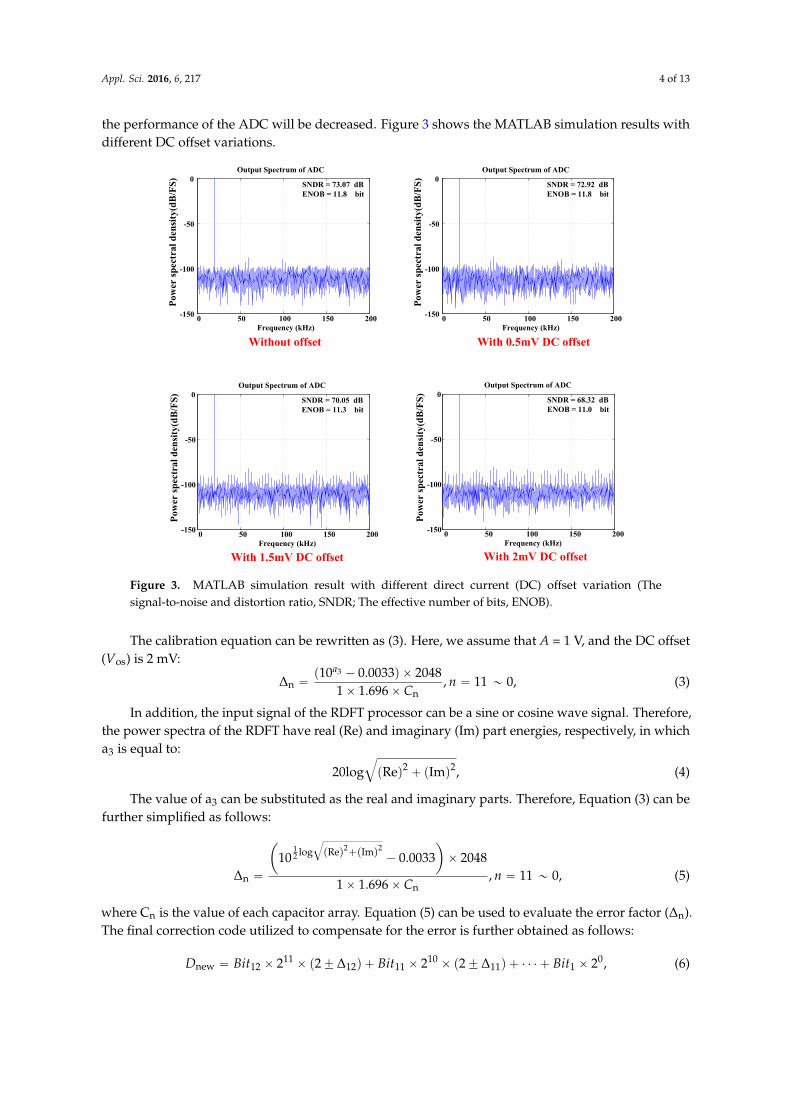
DC offset is a bigger value, the performance of the ADC will be decreased. Figure 3 shows the
MATLAB simulation results with different DC offset variations.
Figure 2. Multi-mode SAR ADC structure.
2.2. Proposed Calibration Method
A previous work [8] derived the proposed calibration formula using the FFT and a cosine waveinput signal. The third harmonic distortion value a3 can be detected by an RDFT processor. The errorfactor ∆n can be further calculated for the calibration. In addition, the calibration code was only usedfor the first-time test to reduce the complexity. This calibration method can not only compensate forthe error caused by the capacitor mismatch and DC offset in the traditional ADC but it can also beapplied to calibrate the T/H circuit in the multi-mode SAR ADC (Figure 2).
The main calibration equation can be written as follows:
a3 “ 20logˆ
Aˆ ∆n ˆ 1.696ˆ Cn
2048` 1.696ˆVos
˙
, (1)
where A is the amplitude of the cosine wave, Cn is the value of each capacitor ratio, ∆n is the errorfactor of each capacitor mismatch, and Vos is the DC offset. The DC offset voltage of the comparatorcircuit can be expressed as:
Vos “
d
ˆ
Vov
2∆RD
RD
˙2`
ˆ
Vov
2∆ pW{LqpW{Lq
˙2` p∆Vtq
2, (2)
where Vov, W/L, and Vt are the overdrive voltage, transistor size, and threshold voltage of thedifferential pair, respectively. According to Equation (2), the threshold voltage is a static offset, whichdoes not affect the dynamic performance of the ADC. Meanwhile, both the overdrive voltage andtransistor size will degrade the ADC performance. Some approaches have been used to overcomethis problem and improve the DC offset, such as reducing the overdrive voltage or increasing thecomparator size. However, the drawbacks of these methods are the decrease in the comparison speedand higher power consumption, respectively. Therefore, the problem can be overcome using the RDFTprocessor in a system-on-a-chip to calibrate the ADC error [8]. Generally, if a DC offset value will bevery small, it will not affect the performance of the ADC. However, if a DC offset is a bigger value,
Appl. Sci. 2016, 6, 217 4 of 13
the performance of the ADC will be decreased. Figure 3 shows the MATLAB simulation results withdifferent DC offset variations.Appl. Sci. 2016, 6, 217 4 of 13
Without offset
0 50 100 150 200-150
-100
-50
0
Frequency (kHz)
Pow
er s
pec
tral
den
sity
(dB
/FS
)Output Spectrum of ADC
SNDR = 73.07 dBENOB = 11.8 bit
With 0.5mV DC offset
0 50 100 150 200-150
-100
-50
0
Frequency (kHz)
Pow
er s
pec
tral
den
sity
(dB
/FS
)
Output Spectrum of ADC
SNDR = 72.92 dBENOB = 11.8 bit
With 1.5mV DC offset With 2mV DC offset
0 50 100 150 200-150
-100
-50
0
Frequency (kHz)
Pow
er s
pec
tral
den
sity
(dB
/FS
)
Output Spectrum of ADC
SNDR = 70.05 dBENOB = 11.3 bit
0 50 100 150 200-150
-100
-50
0
Frequency (kHz)
Pow
er s
pec
tral
den
sity
(dB
/FS
)
Output Spectrum of ADC
SNDR = 68.32 dBENOB = 11.0 bit
Figure 3. MATLAB simulation result with different direct current (DC) offset variation (The
signal‐to‐noise and distortion ratio, SNDR; The effective number of bits, ENOB).
The calibration equation can be rewritten as (3). Here, we assume that A = 1 V, and the DC
offset (Vos) is 2 mV:
3
nn
10 0.0033 2048, 11 ~ 0
1 1.696
a
nC
, (3)
In addition, the input signal of the RDFT processor can be a sine or cosine wave signal.
Therefore, the power spectra of the RDFT have real (Re) and imaginary (Im) part energies,
respectively, in which a3 is equal to:
22 ImRelog20 , (4)
The value of a3 can be substituted as the real and imaginary parts. Therefore, Equation (3) can
be further simplified as follows:
2 21log Re Im
2
nn
10 0.0033 2048
, 11 ~ 01 1.696
nC
, (5)
where Cn is the value of each capacitor array. Equation (5) can be used to evaluate the error factor
(Δn). The final correction code utilized to compensate for the error is further obtained as follows:
11 10 0new 12 12 11 11 12 2 2 2 2D Bit Bit Bit , (6)
The third harmonic distortion can be significantly reduced when the compensation is finished.
The ADC performance can then be improved. In addition, the residue errors are not only
compensated, but also corrected by fine‐tuning.
Figure 3. MATLAB simulation result with different direct current (DC) offset variation (Thesignal-to-noise and distortion ratio, SNDR; The effective number of bits, ENOB).
The calibration equation can be rewritten as (3). Here, we assume that A = 1 V, and the DC offset(Vos) is 2 mV:
∆n “p10a3 ´ 0.0033q ˆ 2048
1ˆ 1.696ˆ Cn, n “ 11 „ 0, (3)
In addition, the input signal of the RDFT processor can be a sine or cosine wave signal. Therefore,the power spectra of the RDFT have real (Re) and imaginary (Im) part energies, respectively, in whicha3 is equal to:
20logb
pReq2 ` pImq2, (4)
The value of a3 can be substituted as the real and imaginary parts. Therefore, Equation (3) can befurther simplified as follows:
∆n “
ˆ
1012 log
b
pReq2`pImq2´ 0.0033
˙
ˆ 2048
1ˆ 1.696ˆ Cn, n “ 11 „ 0, (5)
where Cn is the value of each capacitor array. Equation (5) can be used to evaluate the error factor (∆n).The final correction code utilized to compensate for the error is further obtained as follows:
Dnew “ Bit12 ˆ 211 ˆ p2˘ ∆12q ` Bit11 ˆ 210 ˆ p2˘ ∆11q ` ¨ ¨ ¨ ` Bit1 ˆ 20, (6)
Appl. Sci. 2016, 6, 217 5 of 13
The third harmonic distortion can be significantly reduced when the compensation is finished.The ADC performance can then be improved. In addition, the residue errors are not only compensated,but also corrected by fine-tuning.
2.3. MATLAB Verification
MATLAB is used to simulate and verify the proposed self-testing platform technique andcalibration method and build the behavior model, which includes the 12 bit SAR ADC, RDFTcomputation, signal generator, and proposed calibration. In addition, a 1% capacitor mismatch,2 mV DC offset, thermal noise, sampling jitter and switch nonlinearity are adopted in the 12 bit SARADC model to demonstrate the proposed calibration. Generally, the backgate effect of the switchtransistor is the main source of its resistance nonlinearity. So, the input-dependent switch transistorcan be defined as:
R “1
µCox
´
WL
¯
rVDD ´Vths, (7)
In this work, the parameters of the sampling switch are determined by the virtual process, so thebackgate effect value of this switch transistor is:
Rp “1
86ˆ 10´6 p0.18q r1.8´ p´0.5qs« 0.911k, (8)
Rn “1
387ˆ 0´6 p0.18q r1.8´ 0.5s« 0.358k, (9)
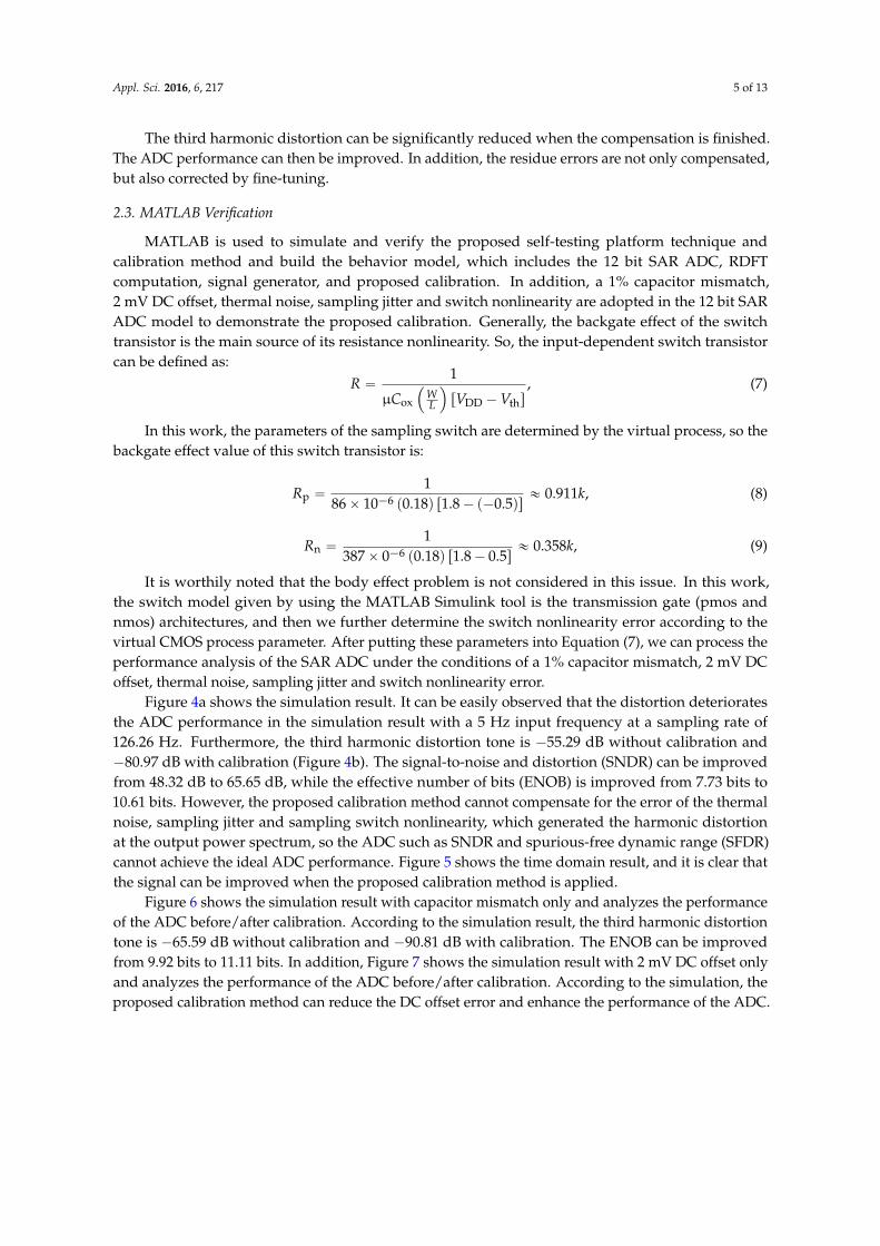
It is worthily noted that the body effect problem is not considered in this issue. In this work,the switch model given by using the MATLAB Simulink tool is the transmission gate (pmos andnmos) architectures, and then we further determine the switch nonlinearity error according to thevirtual CMOS process parameter. After putting these parameters into Equation (7), we can process theperformance analysis of the SAR ADC under the conditions of a 1% capacitor mismatch, 2 mV DCoffset, thermal noise, sampling jitter and switch nonlinearity error.
Figure 4a shows the simulation result. It can be easily observed that the distortion deterioratesthe ADC performance in the simulation result with a 5 Hz input frequency at a sampling rate of126.26 Hz. Furthermore, the third harmonic distortion tone is ´55.29 dB without calibration and´80.97 dB with calibration (Figure 4b). The signal-to-noise and distortion (SNDR) can be improvedfrom 48.32 dB to 65.65 dB, while the effective number of bits (ENOB) is improved from 7.73 bits to10.61 bits. However, the proposed calibration method cannot compensate for the error of the thermalnoise, sampling jitter and sampling switch nonlinearity, which generated the harmonic distortionat the output power spectrum, so the ADC such as SNDR and spurious-free dynamic range (SFDR)cannot achieve the ideal ADC performance. Figure 5 shows the time domain result, and it is clear thatthe signal can be improved when the proposed calibration method is applied.
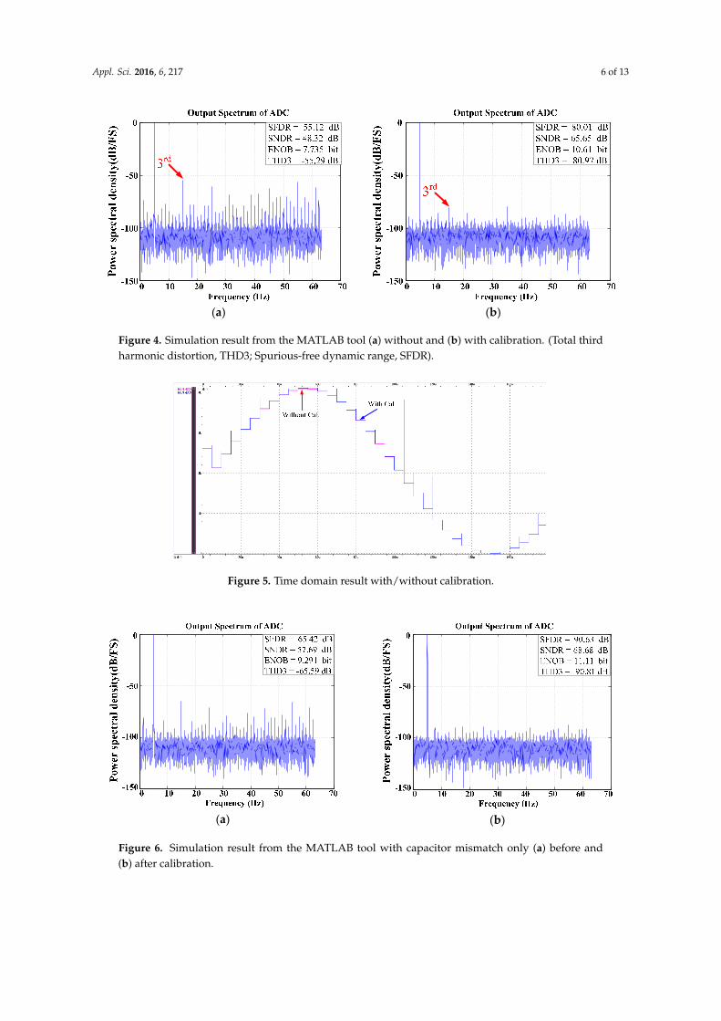
Figure 6 shows the simulation result with capacitor mismatch only and analyzes the performanceof the ADC before/after calibration. According to the simulation result, the third harmonic distortiontone is ´65.59 dB without calibration and ´90.81 dB with calibration. The ENOB can be improvedfrom 9.92 bits to 11.11 bits. In addition, Figure 7 shows the simulation result with 2 mV DC offset onlyand analyzes the performance of the ADC before/after calibration. According to the simulation, theproposed calibration method can reduce the DC offset error and enhance the performance of the ADC.
Appl. Sci. 2016, 6, 217 6 of 13Appl. Sci. 2016, 6, 217 6 of 13
(a)
(b)
Figure 4. Simulation result from the MATLAB tool (a) without and (b) with calibration. (Total third
harmonic distortion, THD3; Spurious‐free dynamic range, SFDR).
Figure 5. Time domain result with/without calibration.
(a)
(b)
Figure 6. Simulation result from the MATLAB tool with capacitor mismatch only (a) before and (b)
after calibration.
Figure 4. Simulation result from the MATLAB tool (a) without and (b) with calibration. (Total thirdharmonic distortion, THD3; Spurious-free dynamic range, SFDR).
Appl. Sci. 2016, 6, 217 6 of 13
(a)
(b)
Figure 4. Simulation result from the MATLAB tool (a) without and (b) with calibration. (Total third
harmonic distortion, THD3; Spurious‐free dynamic range, SFDR).
Figure 5. Time domain result with/without calibration.
(a)
(b)
Figure 6. Simulation result from the MATLAB tool with capacitor mismatch only (a) before and (b)
after calibration.
Figure 5. Time domain result with/without calibration.
Appl. Sci. 2016, 6, 217 6 of 13
(a)
(b)
Figure 4. Simulation result from the MATLAB tool (a) without and (b) with calibration. (Total third
harmonic distortion, THD3; Spurious‐free dynamic range, SFDR).
Figure 5. Time domain result with/without calibration.
(a)
(b)
Figure 6. Simulation result from the MATLAB tool with capacitor mismatch only (a) before and (b)
after calibration. Figure 6. Simulation result from the MATLAB tool with capacitor mismatch only (a) before and(b) after calibration.
Appl. Sci. 2016, 6, 217 7 of 13Appl. Sci. 2016, 6, 217 7 of 13
(a)
(b)
Figure 7. Simulation result from the MATLAB tool with 2 mV DC offset only (a) before and (b) after
calibration.
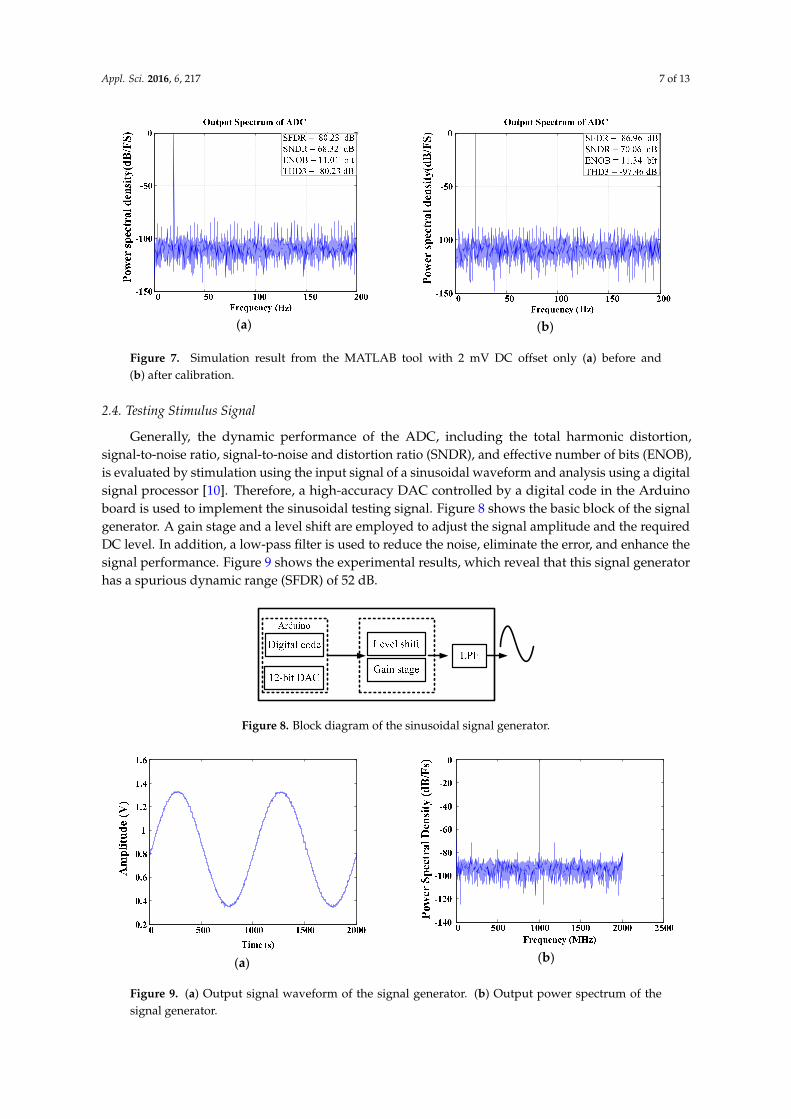
2.4. Testing Stimulus Signal
Generally, the dynamic performance of the ADC, including the total harmonic distortion,
signal‐to‐noise ratio, signal‐to‐noise and distortion ratio (SNDR), and effective number of bits
(ENOB), is evaluated by stimulation using the input signal of a sinusoidal waveform and analysis
using a digital signal processor [10]. Therefore, a high‐accuracy DAC controlled by a digital code in
the Arduino board is used to implement the sinusoidal testing signal. Figure 8 shows the basic
block of the signal generator. A gain stage and a level shift are employed to adjust the signal
amplitude and the required DC level. In addition, a low‐pass filter is used to reduce the noise,
eliminate the error, and enhance the signal performance. Figure 9 shows the experimental results,
which reveal that this signal generator has a spurious dynamic range (SFDR) of 52 dB.
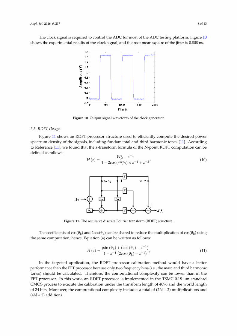
The clock signal is required to control the ADC for most of the ADC testing platform. Figure 10
shows the experimental results of the clock signal, and the root mean square of the jitter is 0.808 ns.
Figure 8. Block diagram of the sinusoidal signal generator.
(a)
(b)
Figure 9. (a) Output signal waveform of the signal generator. (b) Output power spectrum of the
signal generator.
Figure 7. Simulation result from the MATLAB tool with 2 mV DC offset only (a) before and(b) after calibration.
2.4. Testing Stimulus Signal
Generally, the dynamic performance of the ADC, including the total harmonic distortion,signal-to-noise ratio, signal-to-noise and distortion ratio (SNDR), and effective number of bits (ENOB),is evaluated by stimulation using the input signal of a sinusoidal waveform and analysis using a digitalsignal processor [10]. Therefore, a high-accuracy DAC controlled by a digital code in the Arduinoboard is used to implement the sinusoidal testing signal. Figure 8 shows the basic block of the signalgenerator. A gain stage and a level shift are employed to adjust the signal amplitude and the requiredDC level. In addition, a low-pass filter is used to reduce the noise, eliminate the error, and enhance thesignal performance. Figure 9 shows the experimental results, which reveal that this signal generatorhas a spurious dynamic range (SFDR) of 52 dB.
Appl. Sci. 2016, 6, 217 7 of 13
(a)
(b)
Figure 7. Simulation result from the MATLAB tool with 2 mV DC offset only (a) before and (b) after
calibration.
2.4. Testing Stimulus Signal
Generally, the dynamic performance of the ADC, including the total harmonic distortion,
signal‐to‐noise ratio, signal‐to‐noise and distortion ratio (SNDR), and effective number of bits
(ENOB), is evaluated by stimulation using the input signal of a sinusoidal waveform and analysis
using a digital signal processor [10]. Therefore, a high‐accuracy DAC controlled by a digital code in
the Arduino board is used to implement the sinusoidal testing signal. Figure 8 shows the basic
block of the signal generator. A gain stage and a level shift are employed to adjust the signal
amplitude and the required DC level. In addition, a low‐pass filter is used to reduce the noise,
eliminate the error, and enhance the signal performance. Figure 9 shows the experimental results,
which reveal that this signal generator has a spurious dynamic range (SFDR) of 52 dB.
The clock signal is required to control the ADC for most of the ADC testing platform. Figure 10
shows the experimental results of the clock signal, and the root mean square of the jitter is 0.808 ns.
Figure 8. Block diagram of the sinusoidal signal generator.
(a)
(b)
Figure 9. (a) Output signal waveform of the signal generator. (b) Output power spectrum of the
signal generator.
Figure 8. Block diagram of the sinusoidal signal generator.
Appl. Sci. 2016, 6, 217 7 of 13
(a)
(b)
Figure 7. Simulation result from the MATLAB tool with 2 mV DC offset only (a) before and (b) after
calibration.
2.4. Testing Stimulus Signal
Generally, the dynamic performance of the ADC, including the total harmonic distortion,
signal‐to‐noise ratio, signal‐to‐noise and distortion ratio (SNDR), and effective number of bits
(ENOB), is evaluated by stimulation using the input signal of a sinusoidal waveform and analysis
using a digital signal processor [10]. Therefore, a high‐accuracy DAC controlled by a digital code in
the Arduino board is used to implement the sinusoidal testing signal. Figure 8 shows the basic
block of the signal generator. A gain stage and a level shift are employed to adjust the signal
amplitude and the required DC level. In addition, a low‐pass filter is used to reduce the noise,
eliminate the error, and enhance the signal performance. Figure 9 shows the experimental results,
which reveal that this signal generator has a spurious dynamic range (SFDR) of 52 dB.
The clock signal is required to control the ADC for most of the ADC testing platform. Figure 10
shows the experimental results of the clock signal, and the root mean square of the jitter is 0.808 ns.
Figure 8. Block diagram of the sinusoidal signal generator.
(a)
(b)
Figure 9. (a) Output signal waveform of the signal generator. (b) Output power spectrum of the
signal generator. Figure 9. (a) Output signal waveform of the signal generator. (b) Output power spectrum of thesignal generator.
Appl. Sci. 2016, 6, 217 8 of 13
The clock signal is required to control the ADC for most of the ADC testing platform. Figure 10shows the experimental results of the clock signal, and the root mean square of the jitter is 0.808 ns.Appl. Sci. 2016, 6, 217 8 of 13
Figure 10. Output signal waveform of the clock generator.
2.5. RDFT Design
Figure 11 shows an RDFT processor structure used to efficiently compute the desired power
spectrum density of the signals, including fundamental and third harmonic tones [11]. According to
Reference [11], we found that the z‐transform formula of the N‐point RDFT computation can be
defined as follows:
21
1
2cos21
zzNkzW
zHkN
, (10)
The coefficients of cos(θk) and 2cos(θk) can be shared to reduce the multiplication of cos(θk)
using the same computation; hence, Equation (4) can be written as follows:
1
k k
1 1k
sin θ cos θ
1 2cos θ
j zH z
z z
, (11)
In the targeted application, the RDFT processor calibration method would have a better
performance than the FFT processor because only two frequency bins (i.e., the main and third
harmonic tones) should be calculated. Therefore, the computational complexity can be lower than
in the FFT processor. In this work, an RDFT processor is implemented in the TSMC 0.18 μm
standard CMOS process to execute the calibration under the transform length of 4096 and the world
length of 24 bits. Moreover, the computational complexity includes a total of (2N + 2)
multiplications and (4N + 2) additions.
Figure 11. The recursive discrete Fourier transform (RDFT) structure.
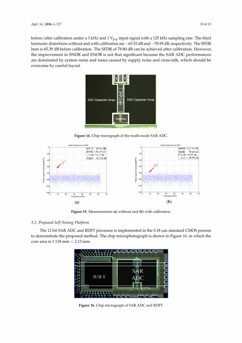
2.6. Processing Flow of the Proposed Self‐Testing Platform
Figure 12 shows the processing flow of the self‐testing platform method. According to the
block diagram, it starts from a sine wave generator with a frequency condition setting, and then a
12 bit DAC output signal is fed into the target SAR ADC. Next, the RDFT processor is used to detect
the third harmonic tone and the proposed calibration formula is employed to calculate the error
Figure 10. Output signal waveform of the clock generator.
2.5. RDFT Design
Figure 11 shows an RDFT processor structure used to efficiently compute the desired powerspectrum density of the signals, including fundamental and third harmonic tones [11]. Accordingto Reference [11], we found that the z-transform formula of the N-point RDFT computation can bedefined as follows:
H pzq “Wk
N ´ z´1
1´ 2cos p2πk{Nq ˆ z´1 ` z´2 , (10)
Appl. Sci. 2016, 6, 217 8 of 13
Figure 10. Output signal waveform of the clock generator.
2.5. RDFT Design
Figure 11 shows an RDFT processor structure used to efficiently compute the desired power
spectrum density of the signals, including fundamental and third harmonic tones [11]. According to
Reference [11], we found that the z‐transform formula of the N‐point RDFT computation can be
defined as follows:
21
1
2cos21
zzNkzW
zHkN
, (10)
The coefficients of cos(θk) and 2cos(θk) can be shared to reduce the multiplication of cos(θk)
using the same computation; hence, Equation (4) can be written as follows:
1
k k
1 1k
sin θ cos θ
1 2cos θ
j zH z
z z
, (11)
In the targeted application, the RDFT processor calibration method would have a better
performance than the FFT processor because only two frequency bins (i.e., the main and third
harmonic tones) should be calculated. Therefore, the computational complexity can be lower than
in the FFT processor. In this work, an RDFT processor is implemented in the TSMC 0.18 μm
standard CMOS process to execute the calibration under the transform length of 4096 and the world
length of 24 bits. Moreover, the computational complexity includes a total of (2N + 2)
multiplications and (4N + 2) additions.
Figure 11. The recursive discrete Fourier transform (RDFT) structure.
2.6. Processing Flow of the Proposed Self‐Testing Platform
Figure 12 shows the processing flow of the self‐testing platform method. According to the
block diagram, it starts from a sine wave generator with a frequency condition setting, and then a
12 bit DAC output signal is fed into the target SAR ADC. Next, the RDFT processor is used to detect
the third harmonic tone and the proposed calibration formula is employed to calculate the error
Figure 11. The recursive discrete Fourier transform (RDFT) structure.
The coefficients of cos(θk) and 2cos(θk) can be shared to reduce the multiplication of cos(θk) usingthe same computation; hence, Equation (4) can be written as follows:
H pzq “jsin pθkq `
`
cos pθkq ´ z´1˘
1´ z´1`
2cos pθkq ´ z´1˘ , (11)
In the targeted application, the RDFT processor calibration method would have a betterperformance than the FFT processor because only two frequency bins (i.e., the main and third harmonictones) should be calculated. Therefore, the computational complexity can be lower than in theFFT processor. In this work, an RDFT processor is implemented in the TSMC 0.18 µm standardCMOS process to execute the calibration under the transform length of 4096 and the world lengthof 24 bits. Moreover, the computational complexity includes a total of (2N + 2) multiplications and(4N + 2) additions.
Appl. Sci. 2016, 6, 217 9 of 13
2.6. Processing Flow of the Proposed Self-Testing Platform
Figure 12 shows the processing flow of the self-testing platform method. According to the blockdiagram, it starts from a sine wave generator with a frequency condition setting, and then a 12 bitDAC output signal is fed into the target SAR ADC. Next, the RDFT processor is used to detect thethird harmonic tone and the proposed calibration formula is employed to calculate the error factor.Finally, we can use this error factor to compensate for the ADC error using the re-coding method.
Appl. Sci. 2016, 6, 217 9 of 13
factor. Finally, we can use this error factor to compensate for the ADC error using the re‐coding
method.
Figure 12. The processing flow of the proposed self‐testing platform.
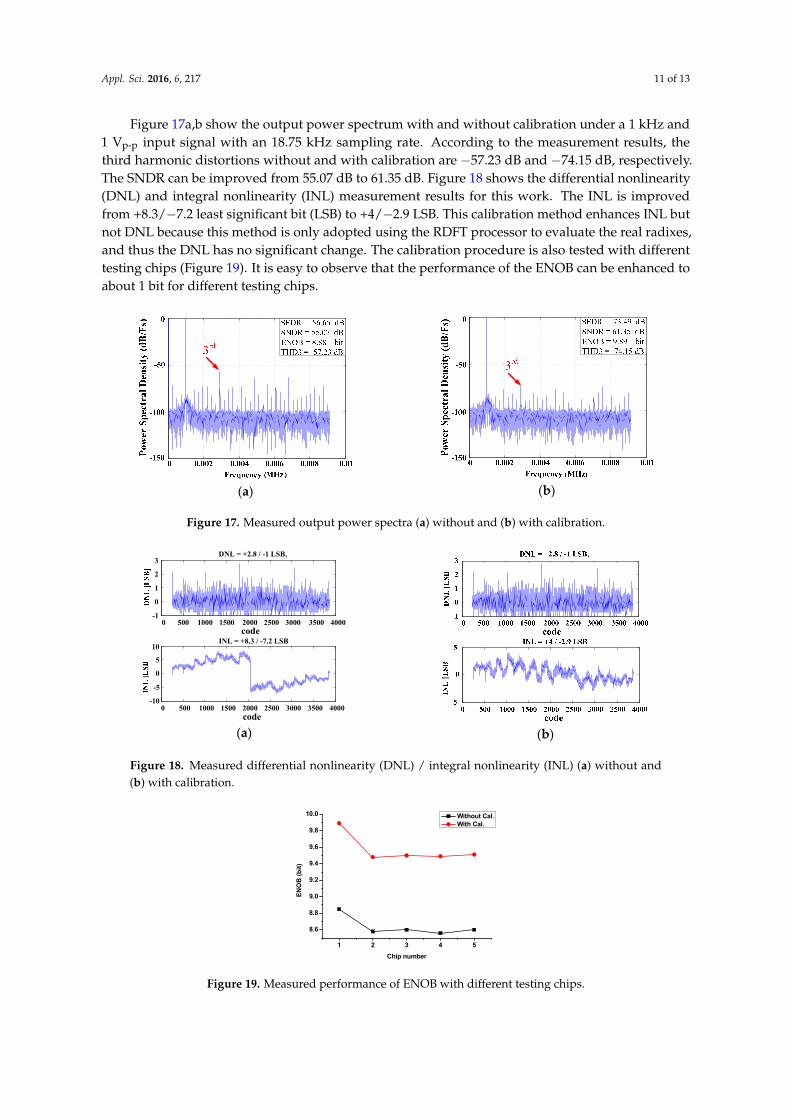
2.7. Proposed Platform Design
The proposed self‐testing platform architecture is illustrated in Figure 13. This platform
includes a power board, clock generator, sinusoidal waveform generator, and testing chip. In the
power board design, the LM317 device is adopted to provide a stable and high‐performance supply
voltage for the testing platform. We can utilize the logic analyzer or the Arduino board to catch the
output data. Finally, the MATLAB tool is adopted to analyze the output signal.
Figure 13. The self‐testing platform architecture.
3. Measurement Results
3.1. Multi‐Mode SAR ADC
A 12 bit multi‐mode SAR ADC is implemented in the 0.18 μm standard CMOS process to
demonstrate the proposed idea. The chip microphotograph is shown in Figure 14, in which the core
circuits have an area of 1.219 mm × 0.938 mm. Figures 15a,b show the output power spectrum
before/after calibration under a 3 kHz and 1 Vp‐p input signal with a 125 kHz sampling rate. The
third harmonic distortions without and with calibration are −65.53 dB and −78.95 dB, respectively.
The SFDR here is 65.39 dB before calibration. The SFDR of 78.80 dB can be achieved after calibration.
However, the improvement in SNDR and ENOB is not that significant because the SAR ADC
performances are dominated by system noise and tones caused by supply noise and cross‐talk,
which should be overcome by careful layout.
Figure 12. The processing flow of the proposed self-testing platform.
2.7. Proposed Platform Design
The proposed self-testing platform architecture is illustrated in Figure 13. This platform includesa power board, clock generator, sinusoidal waveform generator, and testing chip. In the power boarddesign, the LM317 device is adopted to provide a stable and high-performance supply voltage forthe testing platform. We can utilize the logic analyzer or the Arduino board to catch the output data.Finally, the MATLAB tool is adopted to analyze the output signal.
Appl. Sci. 2016, 6, 217 9 of 13
factor. Finally, we can use this error factor to compensate for the ADC error using the re‐coding
method.
Figure 12. The processing flow of the proposed self‐testing platform.
2.7. Proposed Platform Design
The proposed self‐testing platform architecture is illustrated in Figure 13. This platform
includes a power board, clock generator, sinusoidal waveform generator, and testing chip. In the
power board design, the LM317 device is adopted to provide a stable and high‐performance supply
voltage for the testing platform. We can utilize the logic analyzer or the Arduino board to catch the
output data. Finally, the MATLAB tool is adopted to analyze the output signal.
Figure 13. The self‐testing platform architecture.
3. Measurement Results
3.1. Multi‐Mode SAR ADC
A 12 bit multi‐mode SAR ADC is implemented in the 0.18 μm standard CMOS process to
demonstrate the proposed idea. The chip microphotograph is shown in Figure 14, in which the core
circuits have an area of 1.219 mm × 0.938 mm. Figures 15a,b show the output power spectrum
before/after calibration under a 3 kHz and 1 Vp‐p input signal with a 125 kHz sampling rate. The
third harmonic distortions without and with calibration are −65.53 dB and −78.95 dB, respectively.
The SFDR here is 65.39 dB before calibration. The SFDR of 78.80 dB can be achieved after calibration.
However, the improvement in SNDR and ENOB is not that significant because the SAR ADC
performances are dominated by system noise and tones caused by supply noise and cross‐talk,
which should be overcome by careful layout.
Figure 13. The self-testing platform architecture.
3. Measurement Results
3.1. Multi-Mode SAR ADC
A 12 bit multi-mode SAR ADC is implemented in the 0.18 µm standard CMOS process todemonstrate the proposed idea. The chip microphotograph is shown in Figure 14, in which thecore circuits have an area of 1.219 mm ˆ 0.938 mm. Figure 15a,b show the output power spectrum
Appl. Sci. 2016, 6, 217 10 of 13
before/after calibration under a 3 kHz and 1 Vp-p input signal with a 125 kHz sampling rate. The thirdharmonic distortions without and with calibration are´65.53 dB and´78.95 dB, respectively. The SFDRhere is 65.39 dB before calibration. The SFDR of 78.80 dB can be achieved after calibration. However,the improvement in SNDR and ENOB is not that significant because the SAR ADC performancesare dominated by system noise and tones caused by supply noise and cross-talk, which should beovercome by careful layout.Appl. Sci. 2016, 6, 217 10 of 13
Figure 14. Chip micrograph of the multi‐mode SAR ADC.
0 10 20 30 40 50 60 70-140
-120
-100
-80
-60
-40
-20
0
Frequency (kHz)
Pow
er
spec
tral
de
nsit
y(d
B/F
S)
Output Spectrum of ADC
(a)
0 10 20 30 40 50 60 70-140
-120
-100
-80
-60
-40
-20
0
Frequency (kHz)
Pow
er
spec
tral
de
nsity
(dB
/FS
)
Output Spectrum of ADC
(b)
Figure 15. Measurements (a) without and (b) with calibration.
3.2. Proposed Self‐Testing Platform
The 12 bit SAR ADC and RDFT processor is implemented in the 0.18 μm standard CMOS
process to demonstrate the proposed method. The chip microphotograph is shown in Figure 16, in
which the core area is 1.118 mm × 2.13 mm.
Figures 17a,b show the output power spectrum with and without calibration under a 1 kHz
and 1 Vp‐p input signal with an 18.75 kHz sampling rate. According to the measurement results, the
third harmonic distortions without and with calibration are −57.23 dB and −74.15 dB, respectively.
The SNDR can be improved from 55.07 dB to 61.35 dB. Figure 18 shows the differential nonlinearity
(DNL) and integral nonlinearity (INL) measurement results for this work. The INL is improved
from +8.3/−7.2 least significant bit (LSB) to +4/−2.9 LSB. This calibration method enhances INL but
not DNL because this method is only adopted using the RDFT processor to evaluate the real radixes,
and thus the DNL has no significant change. The calibration procedure is also tested with different
testing chips (Figure 19). It is easy to observe that the performance of the ENOB can be enhanced to
about 1 bit for different testing chips.
Figure 16. Chip micrograph of SAR ADC and RDFT.
Figure 14. Chip micrograph of the multi-mode SAR ADC.
Appl. Sci. 2016, 6, 217 10 of 13
Figure 14. Chip micrograph of the multi‐mode SAR ADC.
0 10 20 30 40 50 60 70-140
-120
-100
-80
-60
-40
-20
0
Frequency (kHz)
Pow
er
spec
tral
de
nsit
y(d
B/F
S)
Output Spectrum of ADC
(a)
0 10 20 30 40 50 60 70-140
-120
-100
-80
-60
-40
-20
0
Frequency (kHz)
Pow
er
spec
tral
de
nsity
(dB
/FS
)
Output Spectrum of ADC
(b)
Figure 15. Measurements (a) without and (b) with calibration.
3.2. Proposed Self‐Testing Platform
The 12 bit SAR ADC and RDFT processor is implemented in the 0.18 μm standard CMOS
process to demonstrate the proposed method. The chip microphotograph is shown in Figure 16, in
which the core area is 1.118 mm × 2.13 mm.
Figures 17a,b show the output power spectrum with and without calibration under a 1 kHz
and 1 Vp‐p input signal with an 18.75 kHz sampling rate. According to the measurement results, the
third harmonic distortions without and with calibration are −57.23 dB and −74.15 dB, respectively.
The SNDR can be improved from 55.07 dB to 61.35 dB. Figure 18 shows the differential nonlinearity
(DNL) and integral nonlinearity (INL) measurement results for this work. The INL is improved
from +8.3/−7.2 least significant bit (LSB) to +4/−2.9 LSB. This calibration method enhances INL but
not DNL because this method is only adopted using the RDFT processor to evaluate the real radixes,
and thus the DNL has no significant change. The calibration procedure is also tested with different
testing chips (Figure 19). It is easy to observe that the performance of the ENOB can be enhanced to
about 1 bit for different testing chips.
Figure 16. Chip micrograph of SAR ADC and RDFT.
Figure 15. Measurements (a) without and (b) with calibration.
3.2. Proposed Self-Testing Platform
The 12 bit SAR ADC and RDFT processor is implemented in the 0.18 µm standard CMOS processto demonstrate the proposed method. The chip microphotograph is shown in Figure 16, in which thecore area is 1.118 mm ˆ 2.13 mm.
Appl. Sci. 2016, 6, 217 10 of 13
Figure 14. Chip micrograph of the multi‐mode SAR ADC.
0 10 20 30 40 50 60 70-140
-120
-100
-80
-60
-40
-20
0
Frequency (kHz)
Pow
er
spec
tral
de
nsit
y(d
B/F
S)
Output Spectrum of ADC
(a)
0 10 20 30 40 50 60 70-140
-120
-100
-80
-60
-40
-20
0
Frequency (kHz)
Pow
er
spec
tral
de
nsity
(dB
/FS
)
Output Spectrum of ADC
(b)
Figure 15. Measurements (a) without and (b) with calibration.
3.2. Proposed Self‐Testing Platform
The 12 bit SAR ADC and RDFT processor is implemented in the 0.18 μm standard CMOS
process to demonstrate the proposed method. The chip microphotograph is shown in Figure 16, in
which the core area is 1.118 mm × 2.13 mm.
Figures 17a,b show the output power spectrum with and without calibration under a 1 kHz
and 1 Vp‐p input signal with an 18.75 kHz sampling rate. According to the measurement results, the
third harmonic distortions without and with calibration are −57.23 dB and −74.15 dB, respectively.
The SNDR can be improved from 55.07 dB to 61.35 dB. Figure 18 shows the differential nonlinearity
(DNL) and integral nonlinearity (INL) measurement results for this work. The INL is improved
from +8.3/−7.2 least significant bit (LSB) to +4/−2.9 LSB. This calibration method enhances INL but
not DNL because this method is only adopted using the RDFT processor to evaluate the real radixes,
and thus the DNL has no significant change. The calibration procedure is also tested with different
testing chips (Figure 19). It is easy to observe that the performance of the ENOB can be enhanced to
about 1 bit for different testing chips.
Figure 16. Chip micrograph of SAR ADC and RDFT. Figure 16. Chip micrograph of SAR ADC and RDFT.
Appl. Sci. 2016, 6, 217 11 of 13
Figure 17a,b show the output power spectrum with and without calibration under a 1 kHz and1 Vp-p input signal with an 18.75 kHz sampling rate. According to the measurement results, thethird harmonic distortions without and with calibration are ´57.23 dB and ´74.15 dB, respectively.The SNDR can be improved from 55.07 dB to 61.35 dB. Figure 18 shows the differential nonlinearity(DNL) and integral nonlinearity (INL) measurement results for this work. The INL is improvedfrom +8.3/´7.2 least significant bit (LSB) to +4/´2.9 LSB. This calibration method enhances INL butnot DNL because this method is only adopted using the RDFT processor to evaluate the real radixes,and thus the DNL has no significant change. The calibration procedure is also tested with differenttesting chips (Figure 19). It is easy to observe that the performance of the ENOB can be enhanced toabout 1 bit for different testing chips.Appl. Sci. 2016, 6, 217 11 of 13
(a)
(b)
Figure 17. Measured output power spectra (a) without and (b) with calibration.
0 500 1000 1500 2000 2500 3000 3500 4000-1
0
1
2
3
code
DNL = +2.8 / -1 LSB,
0 500 1000 1500 2000 2500 3000 3500 4000-10
-5
0
5
10
code
INL = +8.3 / -7.2 LSB
(a)
(b)
Figure 18. Measured differential nonlinearity (DNL) / integral nonlinearity (INL) (a) without and (b)
with calibration.
1 2 3 4 5
8.6
8.8
9.0
9.2
9.4
9.6
9.8
10.0
EN
OB
(b
it)
Chip number
Without Cal. With Cal.
Figure 19. Measured performance of ENOB with different testing chips.
Table 1 compares the proposed method and other state‐of‐the‐art ADCs. Although the
proposed method does not have a better performance than that in Reference [12], it still exhibits
better power consumption and area improvement. In addition, the performance of the
split‐capacitive digital‐to‐analog converter (CDAC) method with 0.9 bit improvement is not as good
as that of our proposed method.
Table 1. Comparison of Analog‐to‐Digital Converters (ADCs) with different calibration methods.
JSSCCʹ12 [13] TCASI,13 [14] TVLSI,15 [12] This work
Technology 0.18 μm 0.13 μm 0.6 μm 0.18 μm
Method Dither Split‐CDAC CDAC RDFT
Supply voltage 3.3 V (analog)
1.8 V (digital) 0.5 V 15 V
3.3 V (digital)
1.8 V (analog)
Resolution 10 bit 11 bit 14 bit 12 bit
Figure 17. Measured output power spectra (a) without and (b) with calibration.
Appl. Sci. 2016, 6, 217 11 of 13
(a)
(b)
Figure 17. Measured output power spectra (a) without and (b) with calibration.
0 500 1000 1500 2000 2500 3000 3500 4000-1
0
1
2
3
code
DNL = +2.8 / -1 LSB,
0 500 1000 1500 2000 2500 3000 3500 4000-10
-5
0
5
10
code
INL = +8.3 / -7.2 LSB
(a)
(b)
Figure 18. Measured differential nonlinearity (DNL) / integral nonlinearity (INL) (a) without and (b)
with calibration.
1 2 3 4 5
8.6
8.8
9.0
9.2
9.4
9.6
9.8
10.0
EN
OB
(b
it)
Chip number
Without Cal. With Cal.
Figure 19. Measured performance of ENOB with different testing chips.
Table 1 compares the proposed method and other state‐of‐the‐art ADCs. Although the
proposed method does not have a better performance than that in Reference [12], it still exhibits
better power consumption and area improvement. In addition, the performance of the
split‐capacitive digital‐to‐analog converter (CDAC) method with 0.9 bit improvement is not as good
as that of our proposed method.
Table 1. Comparison of Analog‐to‐Digital Converters (ADCs) with different calibration methods.
JSSCCʹ12 [13] TCASI,13 [14] TVLSI,15 [12] This work
Technology 0.18 μm 0.13 μm 0.6 μm 0.18 μm
Method Dither Split‐CDAC CDAC RDFT
Supply voltage 3.3 V (analog)
1.8 V (digital) 0.5 V 15 V
3.3 V (digital)
1.8 V (analog)
Resolution 10 bit 11 bit 14 bit 12 bit
Figure 18. Measured differential nonlinearity (DNL) / integral nonlinearity (INL) (a) without and(b) with calibration.
Appl. Sci. 2016, 6, 217 11 of 13
(a)
(b)
Figure 17. Measured output power spectra (a) without and (b) with calibration.
0 500 1000 1500 2000 2500 3000 3500 4000-1
0
1
2
3
code
DNL = +2.8 / -1 LSB,
0 500 1000 1500 2000 2500 3000 3500 4000-10
-5
0
5
10
code
INL = +8.3 / -7.2 LSB
(a)
(b)
Figure 18. Measured differential nonlinearity (DNL) / integral nonlinearity (INL) (a) without and (b)
with calibration.
1 2 3 4 5
8.6
8.8
9.0
9.2
9.4
9.6
9.8
10.0
EN
OB
(b
it)
Chip number
Without Cal. With Cal.
Figure 19. Measured performance of ENOB with different testing chips.
Table 1 compares the proposed method and other state‐of‐the‐art ADCs. Although the
proposed method does not have a better performance than that in Reference [12], it still exhibits
better power consumption and area improvement. In addition, the performance of the
split‐capacitive digital‐to‐analog converter (CDAC) method with 0.9 bit improvement is not as good
as that of our proposed method.
Table 1. Comparison of Analog‐to‐Digital Converters (ADCs) with different calibration methods.
JSSCCʹ12 [13] TCASI,13 [14] TVLSI,15 [12] This work
Technology 0.18 μm 0.13 μm 0.6 μm 0.18 μm
Method Dither Split‐CDAC CDAC RDFT
Supply voltage 3.3 V (analog)
1.8 V (digital) 0.5 V 15 V
3.3 V (digital)
1.8 V (analog)
Resolution 10 bit 11 bit 14 bit 12 bit
Figure 19. Measured performance of ENOB with different testing chips.
Appl. Sci. 2016, 6, 217 12 of 13
Table 1 compares the proposed method and other state-of-the-art ADCs. Although the proposedmethod does not have a better performance than that in Reference [12], it still exhibits betterpower consumption and area improvement. In addition, the performance of the split-capacitivedigital-to-analog converter (CDAC) method with 0.9 bit improvement is not as good as that of ourproposed method.
Table 1. Comparison of Analog-to-Digital Converters (ADCs) with different calibration methods.
JSSCC'12 [13] TCASI,13 [14] TVLSI,15 [12] This work
Technology 0.18 µm 0.13 µm 0.6 µm 0.18 µmMethod Dither Split-CDAC CDAC RDFT
Supply voltage 3.3 V (analog)1.8 V (digital) 0.5 V 15 V 3.3 V (digital)
1.8 V (analog)Resolution 10 bit 11 bit 14 bit 12 bit
Sampling rate 768 kS/s 10 kS/s 400 kS/s 18.75 kS/sSNDR (dB) (Wo/Wi) 49.7/60.9 56.5/61.6 61.2/73.3 55.0/61.35ENOB (bit) (Wo/Wi) 7.96/9.83 9.09/9.93 9.88/11.9 8.88/9.89
Power (analog) 58 µW 0.56 µW 90 mW 41.5 µWArea 10.6 mm2 0.58 mm2 9.76 mm2 (only ADC) 2.38 mm2
4. Conclusion and Discussion
In this paper, a self-testing platform with a digital calibration method for SAR ADC is presentedto overcome the non-linearity error of the T/H circuit, the capacitor mismatch of the DAC capacitorarray, and the DC offset of the comparator. The proposed platform has the advantages of low cost andhigh integration without requiring extra analogue circuits or a complex digital calibration algorithm.The testing chip is implemented in the 0.18 µm standard CMOS process. The background signal isanalyzed by the MATLAB tool to demonstrate the calibration algorithm and measured performance.According to the measurement results, the ENOB can be improved by 1 bit.
Acknowledgments: The authors would like to thank the Chip Implementation Center of Taiwan and the Ministryof Science and Technology (MOST) of Taiwan under Grants MOST 104-2218-E-006-022 for their support in thisstudy, as well as the CBIC Lab, APSIC Lab, and Hui-Wen Chang in the CWMI Lab.
Author Contributions: Yi-Hsiang Juan, Hong-Yi Huang, Shuenn-Yuh Lee and Ching-Hsing Luo conceivedand designed the analog circuit, the proposed calibration method, and the experiments. Shin-Chi Lai andWen-Ho Juang provided the digital circuit design and analyzed the data. Yi-Hsing Juan and Shuenn-Yun Leewrote the paper.
Conflicts of Interest: The authors declare no conflict of interest.
References
1. Zou, X.; Xu, X.; Yao, L.; Lian, Y. A 1-V 450-nW fully integrated programmable biomedical sensor interfacechip. IEEE J. Solid-State Circuits. 2009, 44, 1067–1077. [CrossRef]
2. Nakane, H.; Ujiie, R.; Oshima, T.; Yamamoto, T.; Kimura, K.; Okuda, Y.; Tsuiji, K.; Matsuura, T. Afullyintegrated SAR ADC using digital correction technique for triple-mode mobile transceiver. IEEE J.Solid-State Circuits. 2014, 49, 2503–2514. [CrossRef]
3. Balestrieri, E.; Daponte, P.; Rapuano, S. A state of the art on ADC error compensation methods. IEEE Trans.Instrum. Meas. 1987, 54, 1388–1394. [CrossRef]
4. Chang, H.M.; Lin, K.Y.; Cheng, K.T. Tester-assisted calibration and screening for digitally-calibrated ADCs.IEEE Trans. Circuits Syst. I Reg. Pap. 2011, 58, 2838–2848. [CrossRef]
5. Schmidt, C.A.; Lifschitz, O.; Cousseau, J.E.; Figueroa, J.L.; Julián, P. Methodology and measurement setupfor analog-to-digital converter postcompensation. IEEE Trans. Instrum. Meas. 2014, 63, 658–666. [CrossRef]
6. Wang, G.; Kacani, F.; Chiu, Y. IRD digital background calibration of SAR ADC with coarse reference ADCacceleration. IEEE Trans. Circuits Sys. II: Exp. Briefs. 2014, 61, 11–15. [CrossRef]
7. Liang, M.C.; Hsieh, C.H.; Lee, S.Y. A 1.5-bit/stage pipelined ADC with FFT-based calibration method. InProceedings of the 2013 IEEE International Symposium on Circuits and Systems (ISCAS2013), Beijing, China,19–23 May 2013.
Appl. Sci. 2016, 6, 217 13 of 13
8. Juan, Y.H.; Huang, H.Y.; Lai, S.C.; Juang, W.H.; Lee, S.Y.; Luo, C.H. A distortion cancelation technique withthe recursive DFT method for successive approximation analog-to-digital converter. IEEE Trans. Circuits Sys.II Exp. Briefs. 2016, 63, 146–150. [CrossRef]
9. Chang, H.W.; Huang, H.Y.; Juan, Y.H.; Wang, W.S.; Luo, C.H. Adaptive successive approximation ADC forbiomedical acquisition system. Microelectron. J. 2013, 44, 729–735. [CrossRef]
10. Burns, M.; Roberts, G.W. An introduction to mixed-signal IC test and measurement; Oxford University Press:Oxford, UK, 2001.
11. Lai, S.C.; Lei, S.F.; Chang, C.L.; Lin, C.C.; Luo, C.H. Low computational complexity, low power, and low areadesign for the implementation of recursive DFT and IDFT algorithms. IEEE Trans. Circuits Sys. II Exp. Briefs.2009, 56, 921–925. [CrossRef]
12. Thirunakkarasu, S.; Bakkaloglu, B. Built-in self-calibration and digital-trim technique for 14-bit SAR ADCsachieve ˘1 LSB INL. IEEE Trans. Very Large Scale Integr. (VLSI) Sys. 2015, 23, 916–925. [CrossRef]
13. Xu, R.; Liu, B.; Yuan, J. Digitally calibrated 768-kS/s 10-b minimum-size SAR ADC array with dithering.IEEE J. Solid-State Circuits. 2012, 47, 1–12. [CrossRef]
14. Um, J.Y.; Kim, Y.J.; Song, E.W.; Sim, J.Y.; Park, H.J. A digital-domain calibration of split-capacitor DAC fora differential SAR ADC without additional analog circuits. IEEE Trans. Circuits Syst. I Reg. Pap. 2013, 60,2845–2856. [CrossRef]
© 2016 by the authors; licensee MDPI, Basel, Switzerland. This article is an open accessarticle distributed under the terms and conditions of the Creative Commons Attribution(CC-BY) license (http://creativecommons.org/licenses/by/4.0/).