Embed Size (px)
Citation preview

1EDPS-2015 Keynote 150424
A Roadmap for Low-Power Design: Trends, Technology, Tools
Andrew B. KahngUCSD CSE and ECE Departments
[email protected]://vlsicad.ucsd.edu

2EDPS-2015 Keynote 150424
Agenda
RESILIENCEADAPTIVITYTO
APPROXIMATION
FUTURES
TRENDS
DEVICES /CIRCUITS
DESIGNTECHNOLOGYLOW‐
POWER DESIGN

3EDPS-2015 Keynote 150424
Agenda
RESILIENCEADAPTIVITYTO
APPROXIMATION
FUTURES
TRENDS
DEVICES /CIRCUITS
DESIGNTECHNOLOGYLOW‐
POWER DESIGN

4EDPS-2015 Keynote 150424
Trend 1: Race to the End of Roadmap• $$$ for tech, design enablement: go big or go home• Node pacing not slowing despite near-term “red bricks”
• No EUV multi-patterning• No Cu replacement resistivity, rise of MOL / BEOL RC’s, variability• Reliability, layout restrictions less benefit from node (20SOC “lost” like 45nm?)• Especially tough for early-adopter fabless
• Intrinsic mismatch of design-process time constants margins!• Technology development, market definition, architectural design = O(years)• RTL-to-GDS implementation, reliability qualification = O(months)• Fab latency, cycles of yield learning, design re-spins = O(weeks)• Process tweaks, design ECOs = O(days)• Root cause of model-hardware miscorrelation, model guardbanding
• Paper to v1.0 SPICE models: 18 months 12 months at N10• Will see how this works out…

5EDPS-2015 Keynote 150424
Trend 2: Low Power Grand Challenge
• Drivers for semi growth share critical requirement: LOW POWER• Mobility• Big data, green datacenters, cloud• IoT
• Low-power design techniques increase design burden• Added complexity of system + analysis + optimization
• Multiple supply voltages• Multiple voltage domains• Extreme power, clock gating• DVFS• MTCMOS• Multi-Lgate• …

6EDPS-2015 Keynote 150424
Power or Performance?• Cannot escape basic “shape” of tradeoff
• More power reduction (logic, Vt) available when freq • ~Cubic relationship between power and frequency
• New designer mantras• “Highest performance at low power”• “Minimum V for any given throughput”
M. Horowitz, “Scaling, Power and the Future of CMOS”, 2006 Workshop on On- and Off-Chip Interconnection Networks for Multicore Systems
7EDPS-2015 Keynote 150424
Energy vs. Delay: Near-Threshold Computing?• Supply voltage at near-threshold region
>60X power reduction6-8X energy reductionEnables 3D integration
R. G. Dreslinski, et al., “Centip3De: A 64‐Core, 3D Stacked Near‐Threshold System”, HotChips 2012.
8EDPS-2015 Keynote 150424
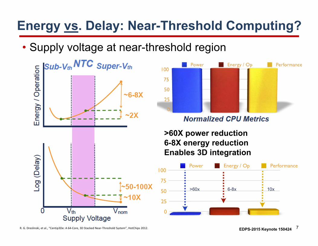
NTC Has Barriers …• Performance loss
• 45nm FO4 delay at NTC supply of 400mV vs. 1.1V: 10X slower
• Increased performance variation• Performance variation due to global process variation alone: ~30% at
1.1V, up to ~400% at 400mV
• Increased functional failure• Random dopant fluctuation, line edge roughness positive feedback of
device mismatch in SRAM
R. G. Dreslinski, et al., “Near‐Threshold Computing: Reclaiming Moore’s Law Through Energy Efficient Integrated Circuits”, Proceedings of the IEEE 98(20) (2010). Pp. 253‐266.

9EDPS-2015 Keynote 150424
… Which Have Workarounds, but• Performance loss
• Cluster-based architecture• Device optimization
• Performance Variation• Soft-edge clocking• Body biasing
• Functional Failure• Alternative SRAM Cells• SRAM robustness analysis• Reconfigurable cache designs
• (FinFET changes the context!)
R. G. Dreslinski, et al., “Near‐Threshold Computing: Reclaiming Moore’s Law Through Energy Efficient Integrated Circuits”, Proceedings of the IEEE 98(20) (2010). Pp. 253‐266.
Body Biasing tech for three target frequencies
Cluster-based architecturevb
FIR filter with soft edge clocking compared to standard flip-flops (SFF); presented with and without useful skew.
Alternative 8 T SRAM cell, decoupling the read and write. Energy of SRAM topologies for 20-
cycle L2 cache across voltages
Alternative L1 cache design with one cache way NTC enabled
10EDPS-2015 Keynote 150424
Agenda
RESILIENCEADAPTIVITYTO
APPROXIMATION
FUTURES
TRENDS
DEVICES /CIRCUITS
DESIGNTECHNOLOGYLOW‐
POWER DESIGN

11EDPS-2015 Keynote 150424
Trend 3: High-Value Equivalent Scaling• Device roadmap (FinFET, FDSOI) helps enormously
• Better electrostatic control • Lower leakage current
TSMC 28nm planar bulk [1] Intel 14nm FinFET [3]ST 20nm FDSOI [2]
[1] http://www.realworldtech.com/iedm-2010/6/[2] S. Natarajan, et al., IEDM 2014, pp. 71-74.[3] Q. Liu, et al., IEDM 2014. pp. 219-222.[4] http://www.itrs.net
400450500550600650700750800850
2011 2012 2013 2014 2015 2016 2017 2018
BULKFDSOIMGFET
(uA/um) [4] ION current

12EDPS-2015 Keynote 150424
FinFET vs. FDSOI for Low-Power Design
FinFET: better subthreshold swing, DIBL [Yeh 10] Performance less sensitive to Vdd lower Vdd, less active power at same speed
FDSOI: more Vt control options [Skotnicki10][PachaASX06][Biesemans]
Metal gate stack changes work function, Vt
Back-plane/gate doping Back-gate biasing
FinFET FDSOI
Surface passivation Yes Yes
HK metal gate stack Yes Yes
BG biasing No Yes
DIBL 70mV/V 80mV/V
Multi‐Vttechniques
Different metal gate stacks
Different BG doping

13EDPS-2015 Keynote 150424
Much Wider Operating Voltage Range • Supply voltage scaling is key low-power technique• Enabled with FinFET, UTBB FDSOI• Complexity explosion: modes, corners in timing
closure
R. Wilson, et al., “ A 460MHz at 397mV, 2.6GHz at 1.3V, 32b VLIW DSP, embedding FMAX tracking”, ISSCC 2014, pp. 452‐454.

14EDPS-2015 Keynote 150424
Design Synthesis/OptArchitecture; RTL; SP&R; Timing/Noise
ECOs
Technology, Design Enablement
SPICE; ITF; Library/IP; Testchips
AnalysisMIS; SHPR; SI; PBA; ‐dynamic
ModelingLVF; BEOL/MOL σ’s; Lib groups
SignoffYield vs. Slack; MCMM; TBC; AVS; Corner vs. Flat Margins
Physical Implementation
OLDNEW
• 1 mode• Setup‐hold• SI• Cw only• NLDM
• MCMM• AVS• Power & Clock gating• Multiple voltage domains• DVFS• MTCMOS• Multi‐Lgate• Cell‐POCV / LVF• Dynamic IR• Wide/exploding corners,
corner reduction, cross‐corners (BEOL Cw, Ccw, RCw, temp, VDD)
• Flat margin selection• Noise closure• Aging/AVS
complexity
Trends 1, 2, 3 Design Closure Nightmare

16EDPS-2015 Keynote 150424
Agenda
RESILIENCEADAPTIVITYTO
APPROXIMATION
FUTURES
TRENDS
DEVICES /CIRCUITS
DESIGNTECHNOLOGYLOW‐
POWER DESIGN

17EDPS-2015 Keynote 150424
Alphabet Soup: DVFS, DCVS, AVS, PVS, SVS…
Multiple Voltage Islands (Multi-VDD)
Dynamic Voltage / Frequency Scaling
VDD1: 1.0V
VDD2: 0.8V
Operating voltage is different, but, voltage has the fixed value
VDD1: 1.0V
VDD2: 0.8 ~ 1.2VOperating voltage and
frequency change according to workload
Adaptive Voltage Scaling
VDD1: 0.9~1.1V
VDD2: 0.8 ~ 1.2VOperating voltage can vary to meet
the performance requirement
(also used to compensateprocess variation)

18EDPS-2015 Keynote 150424
Low-Power Design Roadmap in the ITRSITRS: power and energy = the grand challenge for semiconductor industry low-power design roadmap (2011)
Design Technology Improvement YearImprovements
DescriptionDynamic Static
Low Power Physical Libraries
Before 2011
1.50 1.50 Optimizing transistor size, layout style and cell topology for the standard-cell library
Back Biasing 1.00 1.35 Biasing wells of devices independently of the sources to shift the threshold voltage
Adaptive Body Biasing (ABB) 1.20 2.00 Delivering a positive or negative voltage below a transistor to reduce leakage
Power Gating 0.90 10.00 Turning off the power supplies to idle blocks for leakage reduction
Dynamic Voltage/Frequency Scaling (DVFS) 1.50 1.00 Dynamic management of supply voltage and operating frequency for power reduction
Multilevel Cache Architecture 1.00 1.20 Reduce amount of off-chip memory accesses for performance improvement and power reduction
Hardware Multithreading 1.00 1.30 Using multithreads to improve hardware utilization with leakage reduction
Hardware Virtualization 1.00 1.20 Using one physical server to support multiple guest operating systems simultaneously
Superscalar Architecture 1.00 2.00 Parallel instruction issueing and executing for performance improvement and power reduction
Symmetric Multiple Processing (SMP) 1.50 1.00 Lowering the frequency by using multiple processors and the parallel programming
Software Virtual Prototype 2011 1.23 1.20 Allow the programmer to develop software prior to silicon
Frequency Islands 2013 1.26 1.00 Designing blocks that operate at different frequencies
Near-Threshold Computing 2015 1.23 0.80 Lowering Vdd to 400 - 500 mV
Hardware/Software Co-Partitioning 2017 1.18 1.00 Hardware/software partitioning at the behavioral level based on power
Heterogeneous Parallel Processing (AMP) 2019 1.18 1.00 Using multiple types of processors in a parallel computing architecture
Many Core Software Development Tools 2021 1.20 1.00 Using multiple types of processors in a parallel computing architecture
Power-Aware Software 2023 1.21 1.00 Developing software using power consumption as a parameter
Asynchronous Design 2025 1.21 1.00 Total Non-clock driven design
Total 4.66 0.96
19EDPS-2015 Keynote 150424
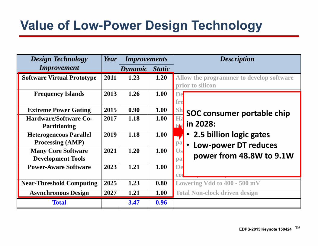
Design Technology Improvement
Year Improvements DescriptionDynamic Static
Software Virtual Prototype 2011 1.23 1.20 Allow the programmer to develop software prior to silicon
Frequency Islands 2013 1.26 1.00 Designing blocks that operate at different frequencies
Extreme Power Gating 2015 0.90 1.00 Shutting down applications (Dark Silicon)Hardware/Software Co-
Partitioning2017 1.18 1.00 Hardware/software partitioning at the
behavioral level based on powerHeterogeneous Parallel
Processing (AMP)2019 1.18 1.00 Using multiple types of processors in a
parallel computing architectureMany Core Software Development Tools
2021 1.20 1.00 Using multiple types of processors in a parallel computing architecture
Power-Aware Software 2023 1.21 1.00 Developing software using power consumption as a parameter
Near-Threshold Computing 2025 1.23 0.80 Lowering Vdd to 400 - 500 mVAsynchronous Design 2027 1.21 1.00 Total Non-clock driven design
Total 3.47 0.96
Value of Low-Power Design Technology
SOC consumer portable chip in 2028: • 2.5 billion logic gates• Low‐power DT reduces power from 48.8W to 9.1W

20EDPS-2015 Keynote 150424
Roadmap: Big Gaps Ahead
• ITRS: power of mobile SOC-CP driver keeps increasing…• … even if envisioned low-power innovations are
developed and deployed on time

21EDPS-2015 Keynote 150424
ADDED in 2013 Low-Power DT RoadmapApproximate Computing
• Variable-accuracy computing (e.g., flexibly from 64b 16b)4D Computing
• Reconfiguration on the flyAdaptivity
• Recapture overdesign from wearout, variation marginsPower Gating Replacement
• HVT device as power switch hits headroom, area wall ?Extreme Heterogeneity
• “coprocessor-dominated architectures” • (pervasive heterogeneity; energy-efficiency from specialization; HW
accelerators)Extreme Power Gating
• Reaching the limits of shut-offSignoff At Typical
• Use adaptivity to recover margin, overdesign

22EDPS-2015 Keynote 150424
Agenda
RESILIENCEADAPTIVITYTO
APPROXIMATION
FUTURES
TRENDS
DEVICES /CIRCUITS
DESIGNTECHNOLOGYLOW‐
POWER DESIGN

23EDPS-2015 Keynote 150424
Resilience = “Long-Term Challenge” in ITRS• Resilience = system product’s ability to mitigate variability,
reliability phenomena• Error detection and repair mechanisms• Alternative guardbanding
mechanisms for different system abstractions: stochastic, approximate, …
• “Cross-layer resilience” = recent buzz-phrase
• Costs, benefits often hazy, difficult to quantify

24EDPS-2015 Keynote 150424
Example Step: Minimize Cost of Resilience• Additional circuits area and power penalties• Recovery from errors throughput degradation• Large hold margin short-path padding cost• Want benefits (e.g., energy) to maximally outweigh costs
Razor Razor-Lite TIMBER
Razor Razor‐Lite TIMBER
Power penalty 30% [Das08] ~0% [Kim13] 100% [Choudhury09]
Area penalty 182% [Kim13] 33% [Kim13] 255% [Chen13]
#recovery cycles 5 [Wan09] 11 [Kim13] 0 [Choudhury09]
25EDPS-2015 Keynote 150424
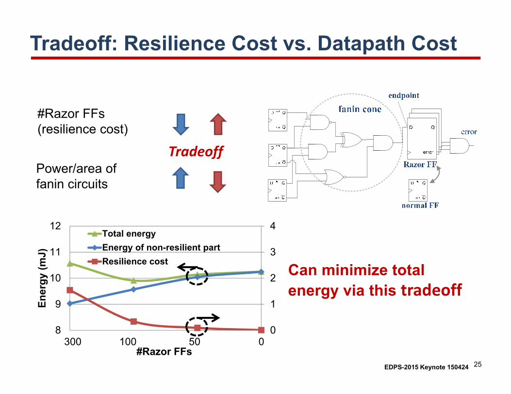
Tradeoff: Resilience Cost vs. Datapath Cost
#Razor FFs (resilience cost)
Power/area of fanin circuits
Tradeoff
0
1
2
3
4
8
9
10
11
12
Ener
gy (m
J)
#Razor FFs
Total energyEnergy of non-resilient partResilience cost
300 100 50 0
Can minimize total energy via this tradeoff
26EDPS-2015 Keynote 150424
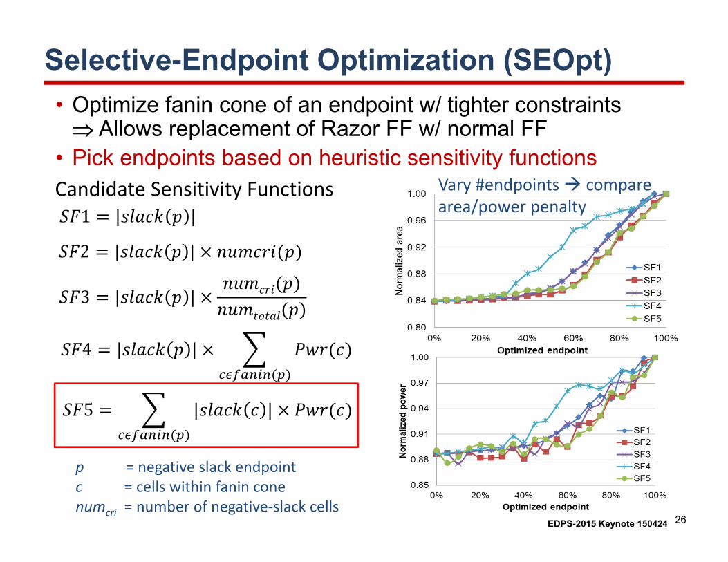
Selective-Endpoint Optimization (SEOpt)• Optimize fanin cone of an endpoint w/ tighter constraints Allows replacement of Razor FF w/ normal FF
• Pick endpoints based on heuristic sensitivity functionsVary #endpoints compare area/power penalty1 | |
2 | |
3 | |
4 | |
5 | |
Candidate Sensitivity Functions
p = negative slack endpointc = cells within fanin conenumcri = number of negative‐slack cells

27EDPS-2015 Keynote 150424
Clock Skew Optimization (SkewOpt)• Increase slacks on timing-critical and/or frequently-
exercised paths1. Generate sequential graph 2. Find cycle of paths with minimum total weight adjust clock latencies contract the cycle into one vertex
3. Iterate Step 2 until all endpoints are optimized
FF1 FF2 FF3W12 W23
ClockData path Clock tree
W31
,1 β ,
Setup slack of path p‐q
Weighting factor
Toggle rate of path p‐q
W’
W’ W’
W’ = average weight on cycle

28EDPS-2015 Keynote 150424
Overall Optimization Flow [GLSVLSI14; ACM TODAES, to appear]
• Iteratively optimize with SEOpt and SkewOptInitial placement
(all FFs = error-tolerant FFs)
Energy < min energy?
Save current solution
Margin insertion on K paths based on sensitivity function
Replace error-tolerant FFs w/ normal FFs
SEOpt
Activity aware clock skew optimization
SkewOpt
OR-tree insertion

29EDPS-2015 Keynote 150424
Benefit of Low-Cost Resilience• Reference flows
• Pure-margin (PM): conventional method w/ only margin insertion• Brute-force (BF): use error-tolerant FFs for timing-critical endpoints
• Proposed method (CO) achieves up to 21% energy reduction compared to reference methods
• Resilience benefits increase with larger process variation
27
29
31
33
35
37
PM BF CO PM BF CO PM BF CO
Ener
gy (m
J)
22
26
30
34
38
PM BF CO PM BF CO PM BF CO
Ener
gy (m
J)
Energy penalty of throughput degradationEnergy penalty of additional circuitsEnergy w/o resilience
Large marginMedium marginSmall margin
MUL
EXU
Large marginMedium marginSmall margin
Small/medium/large margin 1σ/2σ/3σ for SS corner Technology: foundry 28nm

30EDPS-2015 Keynote 150424
Increased Benefit of Resilience with AVS• Adaptive voltage scaling allows a lower supply voltage for resilient
designs, thus reduced power• Proposed method trades off between timing-error penalty vs.
reduced power at a lower supply voltage• Proposed method achieves an average of 17% energy reduction
compared to pure-margin designs Resilience benefits increase in the context of AVS strategy
25
30
35
40
45
50
0.86 0.9 0.94 0.98 1.02
Ener
gy (m
J)
Supply voltage (V)
pure-marginbrute-forceCombOpt
24
26
28
30
32
34
36
0.70 0.72 0.74 0.76 0.78 0.80
Ener
gy (m
J)
Supply voltage (V)
pure-marginbrute-forceCombOpt
MUL EXU
Minimum achievable energy
Technology: foundry 28nm

31EDPS-2015 Keynote 150424
Agenda
RESILIENCEADAPTIVITYTO
APPROXIMATION
FUTURES
TRENDS
DEVICES /CIRCUITS
DESIGNTECHNOLOGYLOW‐
POWER DESIGN

32EDPS-2015 Keynote 150424
A Story of Adaptivity…
Step 1. Design team signs off chip at 1.4 GHz with worst-case (slow silicon) timing corner
Step 2. Chip comes back from fab (typical silicon) and runs at 1.8GHz
[Management is unhappy: pessimism in signoff wasted area, power and design time]
[Cross-functional tiger teams are formed to work on (A) signoff corner pessimism (margin) reduction and (B) improved model-hardware correlation]
Step 3. Scale down supply voltage so chip runs at 1.4 GHz with as little power as possible (= adaptive voltage scaling)

33EDPS-2015 Keynote 150424
Adaptive Voltage Scaling Approaches
Open Loop AVS
Closed-Loop AVS
Error Detection System
Freq. & Vdd LUT
Post-silicon characterization
Generic monitor
Power
Design dependent replica
In-situmonitor
AVS Pre‐characterize LUT [Martin02]
Process‐aware AVSPost‐silicon characterization [Tschanz03]
Process and temperature‐aware AVS Generic on‐chip monitor [Burd00]
Design‐dependent monitor [Elgebaly07,Drake08,Chan12]
In‐situ performance monitor Measure actual critical paths [Hartman06, Fick10]
Error detection and correction system Vdd scaling until error occurs [Das06,Tschanz10]
Application Driven AVSLoading‐aware AVS (software technique)Application‐driven Vdd and frequency scaling [Lin09]

34EDPS-2015 Keynote 150424
“Process-aware Voltage Scaling” (PVS) [ICCAD-2012]
• Monitor design considerations• Critical path can be difficult to identify
(IP from 3rd party)• Multiple modes/voltages: Fmax calibration
requires long test time
• UCSD : generic, tunable monitor• RO-based monitor with Vmin_ro > Vmin
for any data path at any process condition (generic overdesign)
• Monitor is tunable based on Fmax of sample chips to recover design margin (calibrate once)
• Abstracts voltage scaling property instead of matching critical path• Keys: (1) PMOS-, NMOS-dominated
paths determine Vmin; (2) tune ROs with series resistance (pass gates)
PVS RO + SOC Design
Without Fmax of sample chips
With Fmax of sample chips
Store target frequency and RO configurations in a ROM
Configure RO for worst‐case
Configure RO so that all sample
chips meets timing
Closed-Loop AVS

35EDPS-2015 Keynote 150424
Voltage Scaling Basic Concepts
• Process distance: process-induced frequency shift relative to target frequency
• Scaling rate: frequency shift (f) per unit voltage difference (V)
• Vmin= Minimum Vdd to meet target frequency• Calculated from process distance and scaling rate
Voltage
SS
k
targetf
nomV)(kVmin_path
Process distance
Max. freq.Scaling rate =
Vf

36EDPS-2015 Keynote 150424
Process-Aware Voltage Scaling Concept
• Use Vmin of ring-oscillator (RO) as a reference • Design ROs with worst-case voltage scaling
properties an arbitrary circuit will meet target frequency at Vmin_ro
Vmin of ROs Max. Vmin of paths >V
RO
Critical paths
targetf
Freq.
Process corner A
RO
V
Critical paths
targetf
Freq.
Process corner B
Max.

37EDPS-2015 Keynote 150424
Experimental Results on TunabilityAggressive config. Vmin_est < Vmin_chip Some chips will fail
Optimized config.• Increase % high
resistance passgates• Vmin_est ≈ Vmin_chip
Default config.• Low resistance
passgates• Guardband for
worst-case• Vmin_est > Vmin_chip
• 13mV margin

38EDPS-2015 Keynote 150424
Aggressive config. Vmin_est < Vmin_chip Some chips will fail
Default config.• Low resistance
passgates• Guardband for
worst-case• Vmin_est > Vmin_chip
• 13mV margin
Optimized config.• Increase % high
resistance passgates• Vmin_est ≈ Vmin_chip
Benefits of tunability• Compensate for difference
between model vs. silicon• Recover margin when variation is
reduced due to improved process
Experimental Results on Tunability

39EDPS-2015 Keynote 150424
Error-Resilience• Error-freeness guarantees cost {margin, power, $$$}• Unnecessary in some contexts
• Machine learning, data mining, search• Signal processing: image, video, speech• Optimization
• Paradigms for error-resilience• Approximate computing• Stochastic computing• Probabilistic computing• …
• In what contexts, with what knowledge ?
J. Han, M. Orshansky, “Approximate Computing: An Emerging Paradigm For Energy‐Efficient Design”, in Proc. ETS, 2013, pp. 1‐6.
H. Esmaeilzadeh, “Approximation: Beyond the Tyranny of Digital Computing”, IEEE RCS 2, May 2014

40EDPS-2015 Keynote 150424
What If We Knew…(switching activity, workload)
Error‐Tolerant Design
CPU, heal thyself ...
Errors are detected and corrected with redundancy technique
Problem: • Many paths have near‐critical slack → wall of (critical) slack
• Scaling beyond the critical operating point causes massive errors that cannot be corrected
Frequently‐exercised paths: upsize cellsRarely‐exercised paths: downsize cells
Reshape slack distribution for gracefully increasing error rate
Scale voltage further
41EDPS-2015 Keynote 150424
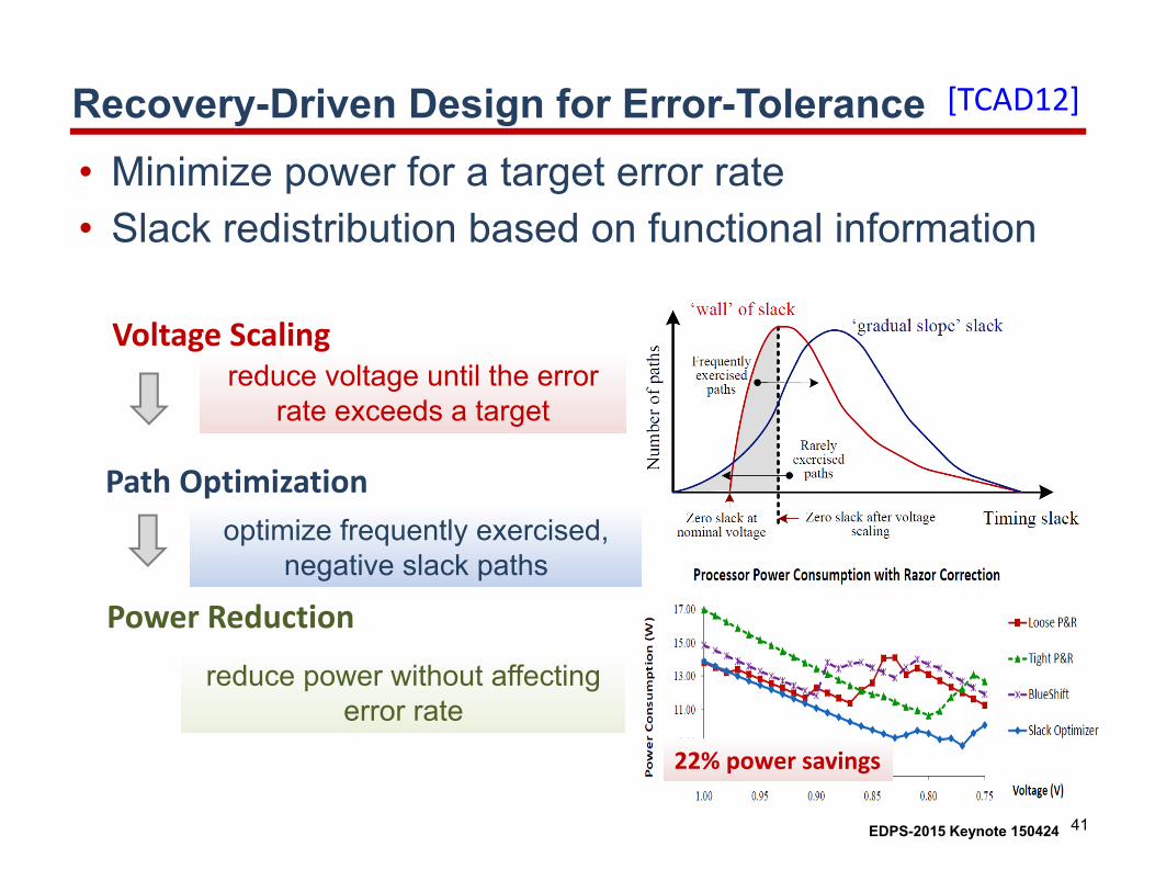
Recovery-Driven Design for Error-Tolerance• Minimize power for a target error rate• Slack redistribution based on functional information
[TCAD12]
Power Reduction
reduce voltage until the error rate exceeds a target
optimize frequently exercised, negative slack paths
reduce power without affecting error rate
Voltage Scaling
Path Optimization
22% power savings

42EDPS-2015 Keynote 150424
What If We Knew … (accuracy requirements)
Problem: • Accuracy requirement can change during runtime benefits of approximation could be reduced
Adapt to changing requirements with runtime accuracy configuration
[DAC 2012]“accuracy‐configurableapproximate adder”
Approximate DesignWhat is the square root of 10 ?
“a little more than three”
“3.162278...”Approximation could be faster and more powerful
higher accuracylower power consumption
43EDPS-2015 Keynote 150424
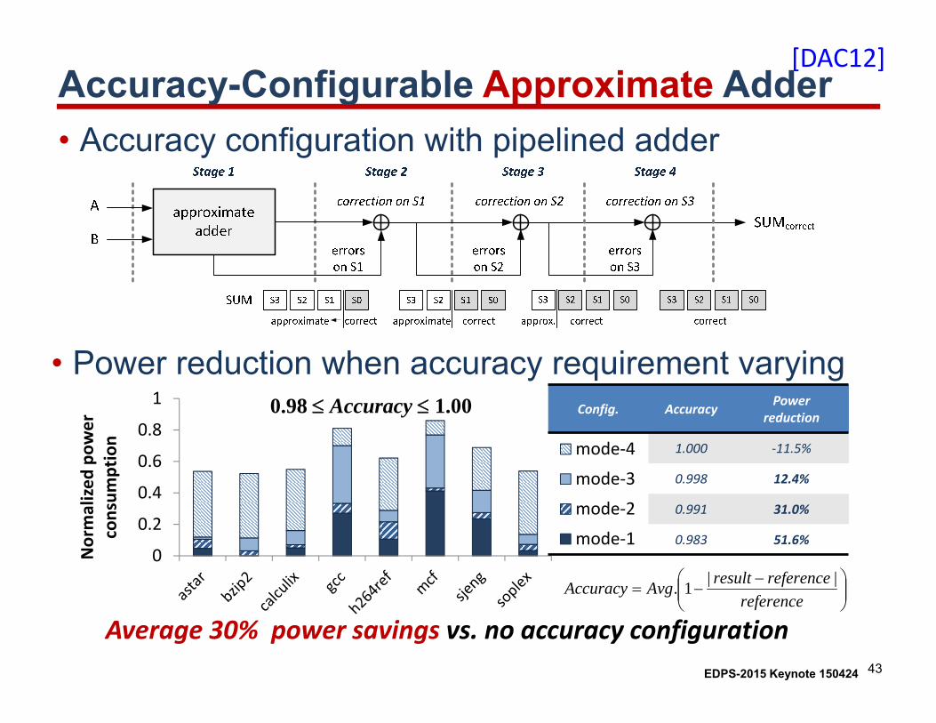
Accuracy-Configurable Approximate Adder
• Power reduction when accuracy requirement varying
0
0.2
0.4
0.6
0.8
1
Normalize
d po
wer
consum
ption mode‐4
mode‐3
mode‐2
mode‐1
0.98 Accuracy 1.00
Average 30% power savings vs. no accuracy configuration
referencereferenceresultAvgAccuracy ||1.
Config. Accuracy Power reduction
1.000 ‐11.5%
0.998 12.4%
0.991 31.0%
0.983 51.6%
[DAC12]
• Accuracy configuration with pipelined adder

44EDPS-2015 Keynote 150424
Stochastic Computing
SC, clock period = 200ps
Conventional, clock period = 400ps
• Conventional computation circuits rely on parallel bits aligned by clock timing errors can be fatal (e.g., if occurring in MSB)
• Stochastic Circuit (SC) paradigm replaces parallel bits with serial bit-stream resilient to voltage scaling
Example: Z= ¼+ ½ ∙ X1∙X2 SC is resilient to voltage scaling

45EDPS-2015 Keynote 150424
Agenda
RESILIENCEADAPTIVITYTO
APPROXIMATION
FUTURES
TRENDS
DEVICES /CIRCUITS
DESIGNTECHNOLOGYLOW‐
POWER DESIGN

46EDPS-2015 Keynote 150424
Better Optimizations• Better MCMM gate sizing
• Gate sizing with single timing view can induce timing violations in other timing view ⇒ multi-corner-multi-mode (MCMM) optimization is needed
• Better FinFET fin discreteness-aware optimization• E.g., PlaceOpt to comprehend and
avoid change in diffusion height induced by different number of fins
• Better design-technology co-optimization• E.g., BEOL stack optimizations, FEOL-BEOL gear ratio and library co-
optimization for PPA, …
#Fin= 6 Diffusion area
W > Wmin
#Fin= 4
Critical in view1
Critical in view2
C1
C2
C5C3
C4
C6
Upsizing C2 for view 1 ⇒ Delay C1 ↑ in view 2⇒ Upsizing C5 for view 2 ⇒ Delay C2 ↑ in view 1⇒ Upsizing C4 for view 1 ⇒ Delay C6 ↑ in view 2⇒….

47EDPS-2015 Keynote 150424
• Silicon characterization, power models validation, silicon to model correlation
• Power and thermal verification and modeling
• Adaptive design (on die sensors, process aware voltage scaling, process, power and temperature monitors). Power models (upf/cpf)
• Process selection ((Bulk CMOS, SOI, FinFET) and device definition (nmos, pmos etc). Process optimization and DFM.
• IP design:Circuit design, Physical implementation of the IP
• Physical design (chip/block level) (back end design)• Power aware RTL implementation/synthesis (front end design)
• System level design• Architectural design• Software optimization and SW‐HW co‐design
System Thinking: Design Synergy• Low power implementation for the modern system on chip
(SOC) requires a holistic and concurrent approach which includes collaboration between:
S. Dobre, UCSD lecture, 2015.

48EDPS-2015 Keynote 150424
Example: Power and Performance Meters• Power and performance meters:
• Hardware–software solution• Measures performance and power in real time for different sub-systems
integrated in the system on chip • Provides feedback to the system for:
• Power management• Thermal management• Workload optimization
S. Dobre, UCSD lecture, 2015.

49EDPS-2015 Keynote 150424
What If We Knew…(scenarios, duty cycles)
• DVFS allows adaptation to workloads, operating conditions• DVFS processor operates at multiple power/performance
points with different lifetimes• Lifetime energy can be different in each scenario (R * X)
Different duty cycle (R) Different frequency scaling (X)
clock frequency of low‐perf mode
clock frequency of high‐perf mode
X =Lifetime
e.g., talk mode
e.g., standby mode

50EDPS-2015 Keynote 150424
Context-Aware Multi-Mode Low-Power Design
Minimize lifetime energy based on modes, duty cycles
Multi‐mode design
• CTL module has 12% energy savings through replication
Selective‐replication design
• Processor‐level: selective replication gives 12% total energy savings with 10% area overhead

51EDPS-2015 Keynote 150424
Lower Power With 3DIC
3DIC % delta power benefit relative to 2DIC Implementation
• Power = key value proposition for 3DICs (shorter / wider connections)• Recent work (DAC-2015): 3DIC power reduction at 28nm foundry FDSOI
libraries and estimation of 3D power benefits only from 2D implementations • Power benefit with 3D varies with testcases and implementation styles
• Percentage delta benefit ranges from -5.1% (i.e., power increases in 3DIC) to 16.0%
3DIC Implementation and Modeling flow
3D structure: F2B and F2F
‐10
‐5
0
5
10
15
20
THEIA (GPU
)
OST2 (CPU
)
Viterbi (Mod
em)
DCT
(Multim
edia)
AES (PE)
Delta Pow
er (%
)
Testcases
Min Max Mean

52EDPS-2015 Keynote 150424
Clock (well-known, but still on table)• Clocking = ~30-40% of total power• SOC complexity: 1000+ clock domains• Clock architecture: Many frequencies, local dividers to reduce frequency• SP&R: planning, placement, buffering of “top-level”: CGCs, MUXes, dividers• CTS: MCMM skew reduction, skew variation reduction (high voltage is wire-
dominated but low voltage is gate-dominated, large hold buffering costs, …)• Routing: NDRs, routing with distributed drivers, long common paths
(reduces wirelength, driver sizes and number of clock buffers)
T.-B. Chan, K. Han, A. B. Kahng, J.-G. Lee and S. Nath, "OCV-Aware Top-Level Clock Tree Optimization", Proc. Great Lakes Symposium on VLSI, 2014, pp. 33-38.
53EDPS-2015 Keynote 150424
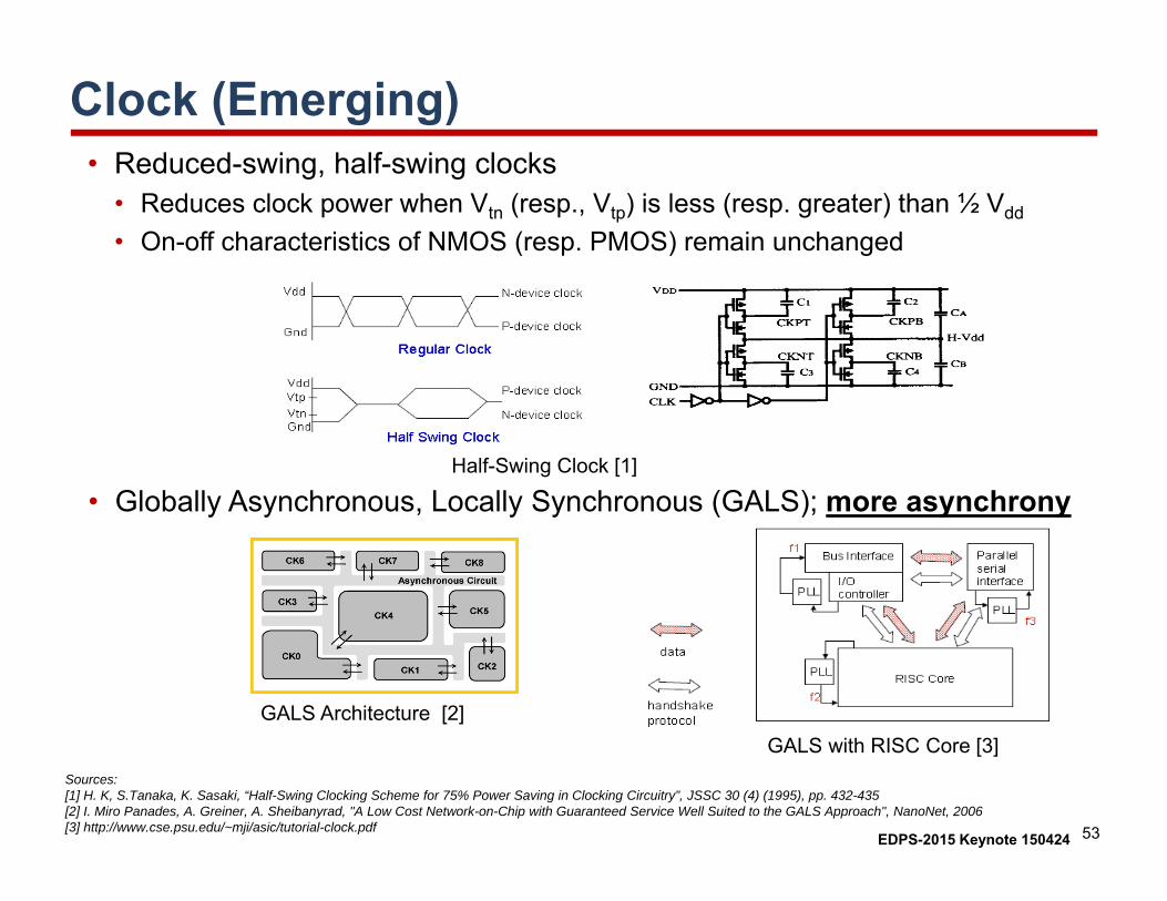
Clock (Emerging)• Reduced-swing, half-swing clocks
• Reduces clock power when Vtn (resp., Vtp) is less (resp. greater) than ½ Vdd
• On-off characteristics of NMOS (resp. PMOS) remain unchanged
• Globally Asynchronous, Locally Synchronous (GALS); more asynchronyHalf-Swing Clock [1]
GALS Architecture [2]GALS with RISC Core [3]
Sources: [1] H. K, S.Tanaka, K. Sasaki, “Half-Swing Clocking Scheme for 75% Power Saving in Clocking Circuitry”, JSSC 30 (4) (1995), pp. 432-435[2] I. Miro Panades, A. Greiner, A. Sheibanyrad, "A Low Cost Network-on-Chip with Guaranteed Service Well Suited to the GALS Approach", NanoNet, 2006[3] http://www.cse.psu.edu/~mji/asic/tutorial-clock.pdf
54EDPS-2015 Keynote 150424
A Few Nutshells…• AVS mandatory to address variation at low voltage• NTC in use as “ultra-low voltage mode”; standard design
enablement works out of box in FinFET nodes (e.g., 0.46V – 1.25V)• FinFET transition has large benefits takes some pressure off
of low-power design in near term (?)• Next-generation optimizers needed for DVFS/MCMM, wide
voltage corners, multi-patterning, FinFET discreteness, …• Next-generation analysis tools/flows (thermal, dynamic IR,
reliability wearout, stress = “next loops to close”) to further squeeze design margin
• Active power regains focus clock power reduction, active leakage cost, design for min V at given throughput
• System-level low-power design continues as both (complexity) challenge and (cross-layer) opportunity
• 3DIC will turn the corner for power-performance envelope• Approximate computing will take longer to turn the corner …

55EDPS-2015 Keynote 150424
THANK YOU!