Embed Size (px)
Citation preview

CPSS TRANSACTIONS ON POWER ELECTRONICS AND APPLICATIONS, VOL. 2, NO. 3, SEPTEMBER 2017170
Abstract—Silicon-Carbide (SiC) devices with superior perfor-mance over traditional silicon power devices have become the prime candidates for future high-performance power electronics energy conversion. Traditional device packaging becomes a lim-iting factor in fully realizing the benefits offered by SiC power devices, and thus, improved and advanced packaging structures are required to bridge the gap between SiC devices and their applications. This paper provides a review of the state-of-art ad-vanced module packaging technologies for SiC devices with the focuses on module layout, packaging material system, and module integration trend, and links these packaging advancements to their impacts on the SiC device performances. Through this review, the paper discusses main challenges and potential solutions for SiC modules, which is critical for future SiC applications.
Index Terms—Packaging material system, power module in-tegration, SiC advanced packaging.
I. IntroductIon
RAPID development in power electronics systems poses strong demand for better power semiconductor devices.
Silicon (Si) device has been dominating in this area for de-cades, and now it almost hits the material theoretical limita-tions [1] for further improvement on the device’s switching and conduction performances. Therefore, Wide Bandgap (WBG) material based devices start to attract attention of power electronics engineers.
Compared to Si power devices, WBG power semiconductors has lower intrinsic carrier concentration (10-35 orders of mag-nitude), higher electric breakdown field (4-20 times), higher thermal conductivity (3-13 times), and larger saturated electron drift velocity (2-2.5 times) [2]. Translating these characteristics into device specifications, given the same die size and thick-ness, WBG devices can provide higher breakdown voltage, higher current, higher operating temperature, higher switching speed and lower switching loss over Si devices. TABLE I [3], [4] summaries the figure-of-merit comparisons for WBG and Si devices, which shows that, theoretically, the performance of SiC and GaN devices surpasses that of Si devices regarding switching loss, switching speed and current density with orders
of magnitude. However, these outstanding benefits cannot be demonstrated in power electronics converters on the same scale due to the packaging limitations [5]-[9]. Power device packag-ing, which is the bridge between power device and its applica-tion, has become a bottleneck for WBG device applications [10]. The challenges in SiC power module packaging are brought by the unique characteristics of SiC devices, which can be summa-rized in following aspects:
A. High Switching Speed (dV/dt and di/dt)
Compared to Silicon devices, SiC device has much lower Coss and Qg, and they can switch at much higher dV/dt and di/dt [11]. High switching speed enables low switching loss and high switching frequency, which can potentially improve the converter power density and efficiency. Nevertheless, this new feature poses strong challenges for parasitic control. With the same amount of parasitic inductance, higher di/dt will generate higher voltage overshoot and ringing across the device, which can significantly increase the device switching losses, device voltage stresses and EMI noises. With the same amount of par-asitic capacitance, higher dV/dt will result in higher common mode noise, which can increase the load for EMI filtering in converters.
High switching speed also brings challenges in device par-alleling. Multi-chip parallel operating is an effective way for power scaling at the module level. Current balancing in both steady-state and dynamic region is the key design consideration
Manuscript received September 11, 2017. This work was supported by the National Natural Science Foundation of China under Grant 51507069.
C. Chen and Y. Kang are with the School of Electrical and Electronic Engineering, Huazhong University of Science and Technology, Wuhan, China (e-mail: [email protected]; [email protected]). F. Luo is with the Department of Electrical Engineering, University of Arkansas, Fayetteville, USA (e-mail: [email protected]).
Digital Object Identifier 10.24295/CPSSTPEA.2017.00017
A Review of SiC Power Module Packaging: Layout, Material System and Integration
Cai Chen, Fang Luo, and Yong Kang
TABLE I mAIn fIgure-of-merIt compArIsons for WBg And sI
poWer semIconductors
Si GaAs 6H-SiC 4H-SiC GaN Diamond
JFMBFMFSFMBSFMFPFMFTFM
1.01.01.01.01.01.0
1.814.811.41.63.640.7
277.8125.330.513.148.3
1470.5
215.1223.161.212.956.0
3424.8
215.1186.765.052.530.4
1973.6
8100025106359524021476
5304459
JFM : Johnson’s figure of merit is a measure of the ultimate high frequencycapability of the material.BFM : Baliga’s figure of merit is a measure of the specific on-resistance of the drift region of a vertical FETFSFM : FET switching speed figure of meritBSFM : Bipolar switching speed figure of meritFPFM : FET power handling capacity figure of meritFTFM : FET power switching productBPFM : Bipolar power handling capacity figure of meritBTFM : Bipolar power switching product figure of merits

171
in device paralleling, which is usually realized by symmetrical layouts for the paralleled devices. High switching speed in-creases the sensitivity of parasitic symmetry makes it difficult to maintain current balance at high switching speed.
B. High Operation Temperature and High Electric-Field
SiC device provides the potential to achieve higher power density, which means the power package for SiC devices will also need to take much higher loss density. SiC device has the extraordinary capability for high-temperature operation up to 200°C -300°C. This temperature has been way beyond the suitable range for traditional packaging material systems for Si devices, which usually no higher than 175°C. It is important to search for new packaging material systems which can reliably sustain such a high-temperature operation.
For the same breakdown voltage, SiC device die is much thinner than SiC devices. This feature leads to challenges on the mechanical stability considerations for SiC power module packaging. Selections of appropriate substrates, die-attachment materials and encapsulation material to match with the thermal expansion coefficient of the SiC devices are the key factors to the success of SiC packaging.
Due to the same thin die thickness feature, to handle the same voltage, SiC device package will need to sustain higher electric field than that in Si power device packages. This new feature re-quires new insulation packaging materials to support in device applications.
In response to these challenges, this paper provides a review
from three approaches including advanced module layout, ma-terial system selection and module integration. Each approach provides a solution to one or a couple of the challenges listed above. For a fair comparison, this paper firstly presents an over-view of the state-of-the-art packaging approaches for commer-cially available SiC devices, and then this paper summaries the new advancement in research works for advanced packaging structure, packaging material systems and the module integra-tion trend, from both academia and industry. The prospected trend for the future of SiC module packaging is included in the last part of this paper.
II. the stAte-of-the-Art for commercIAlly AvAIlABle sIc poWer devIces
Driven by the emerging market, SiC device manufactures tried best to pull available resources together to provide their products to meet users’ demand. TABLE II and TABLE III list major SiC manufacturers with their product specifications [12]-[16], which present the state-of-the-art packaging for commer-cially available SiC power products, as summarized below:
SiC discrete devices are available from 650 V to 1700 V while maximum rated current is around 120 A. In this range, TO247/220/263 and SOT 227 packages are the dominating forms of power devices. There are varieties on the pin-configu-rations and Kelvin Gate structure in these traditional packages. However, the nature of TO and SOT packages introduce high parasitic power loop inductances (usually around 20-30 nH) and high thermal impedance, which reduces the benefit of using SiC devices [17].
SiC Power modules are commercially available from Wolf-speed, RHOM, GeneSiC, Infineon and SEMIKRON [18]-[22]. Both Wolfspeed and RHOM provide 2-level, half-bridge, and phase-leg modules. RHOM’s module is in an EconoDual package, which is similar to the state-of-the–art IGBT package. Its packaging loop inductance is around 15 nH. Wolfspeed provides different packages from its product line for different applications. 63 mm standard packaged modules. This tradi-tional package has been widely adopted by high power Si IGBT devices. It provides benefits of high technical maturity and low cost. However, this package also comes with obvious disadvan-tages including high parasitic loop inductance (15 nH- 20 nH), moderate thermal impedances and heavy packaging weight. These features can potentially limit the performance of WBG devices. To address those problems, Wolfspeed announced their new generation SiC modules in their new HT package. The new design has 9 nH power loop inductance with ultra-light weight and improved thermal management. These are enabling features to unleash the potential of WBG devices. The module from GenSiC consists of a single switch instead of a phase-leg. It is in SOT-227 package, which is a standard package for Si power switches. Infineon and SEMIKRON also launched new full SiC power module and the inductance can be reduced to 15 nH.
Commercially available packages support device junction temperature up to 200°C (from STMicroelectronics and CREE), most of the off-shelf modules stays with the same temperature range as Si modules (150 °C -175°C).
Fig. 1. Some commercial SiC power module packages: (a) Infineon Easy1B, (b) SEMIKRON MiniSKiiP, (c) SEMIKRON SEMITOP, (d) Wolf-speed 62 mm, (e) Wolfspeed high Performance 62 mm, (f) ROHM type C.
(a)
(c)
(e)
(b)
(d)
(f)
C. CHEN et al.: A REVIEW OF SIC POWER MODULE PACKAGING: LAYOUT, MATERIAL SYSTEM AND INTEGRATION

172 CPSS TRANSACTIONS ON POWER ELECTRONICS AND APPLICATIONS, VOL. 2, NO. 3, SEPTEMBER 2017
These two tables shows that most of the SiC power device manufacturers provide their SiC devices with traditional pack-ages due to the low cost and timely market availability. Al-though the industry has been aware of the importance of power module packaging for SiC device, the demand on advanced power package has not yet been matched with its research and development.
III. AdvAnced pAckAgIng structures
A standard traditional power module package (as shown in Fig. 2, insert a picture here) includes a 7-layer structure, includ-ing a heat-sink, a base-plate, a DBC substrate, and die-attach-ments between these layers. The top side of the device is usually wire-bonded to external lead-frames, while the bottom side of the device is attached onto the DBC traces. The current flow in the device goes from the bottom contact vertically through the device and bond-wires to the terminals of the module. The module is often filled with encapsulation material to prevent the device and bond-wires from environment contamination/vibra-tion. This module structure usually comes with high parasitic power loop inductance ranging from 20 nH to 30 nH.
As stated in the introduction, SiC device has high speed switching capability, which makes the device is sensitive to its packaging parasitics. Parasitic inductance in the power module
induces high voltage overshoot and ringing on switching de-vices, which then increases the device switching loss [23] and EMI emission from the modules. Advanced packaging structure can significantly help to minimize of the loop parasitics by opti-mizing its current commutation loop layout within the package. Therefore, advanced packaging structure can sufficiently realize high efficiency and high frequency switching operation using SiC devices. By reducing the voltage ringing at high switching speed, this type of designs can also reduce the EMI emission from the power module.
The other benefit of using advanced packaging structure is
TABLE IIcommercIAl dIscrete sIc devIces
Manufacturer Wolfspeed ROHM USCi STMicroelectronics
Voltage (V) 900 1000 1200 1700 650 1200 1700 650 1200 1200 650 1200
Technology SiC MOSFET SiC MOSFET SiC Cascode SiC JFET SiC MOSFET
Package TO247/TO263
TO247/TO263
TO247/TO247
TO247/TO263
TO247/TO220 TO247 TO247/
TO268 TO247 TO247 TO247 TO247 TO247
Current (A) 11.5 - 36 22 - 35 10 - 90 5 - 72 29 - 118 10 - 95 6 20 20 - 35 21 - 38 100 12 - 65Operating Tem-
perature (°C) 150 150 150 150 175 175 175 150 150 175 200 200
Coss (pF) 20 - 60 40 - 60 23 - 220 12 - 171 35 - 148 41- 237 19 178 57 53000 305 30 - 170
Ron (mΩ) 65 - 280 65 - 120 25 - 280 45 - 1000 17 - 120 22 - 160 750 45 60 - 100 45 - 80 22 69 - 690
Qg (nC) 9.5 - 30.4 21.5 - 35 20.4 - 161 13 - 188 172 42 - 178 17 47.5 47.5 62 215 22 - 122
TABLE IIIcommercIAl sIc poWer modules
Manufacturer Wolfspeed ROHM GeneSiC Infineon SEMIKRON
Voltage (V) 1200 1700 1200 1200 1200
Package 45mm/62mm/High Performance 62mm 62mm Type C/E TO247/SOT227/TO263 AG-EASY1B-2 MiniSKiiP/ SEMITOP/ SEMI-
PACK/ SEMITRANSCurrent (A) 20 - 325 225 80 - 300 25 - 160 50 - 100 14 - 541
Operating Tempera-ture (°C) 150 - 175 150 150 - 175 175 150 175
Coss (pF) 100 - 2570 2500 2000 - 4000 >440000 470 NC - 1644
Ron (mΩ) 3.6 - 80 8 9.67 - 43.75 10 - 100 11 - 23 NC
Qg (nC) 270 - 3200 4400 560 - 1500 55 62 - 250 NC - 2268
Fig. 2. The cross-section of a traditional wire-bonded power module.
CASE SiC DEVICES
SUBSTRATEWIREBONDS
HEAT SINKBASEPLATE
TerminalLeads

173
possibility of “double-side cooling”. These structures, especially “wire-less” structures, provide two paralleled cooling paths for the SiC device from both top and bottom. This type of designs can tremendously reduce the equivalent “junction-to-ambient” thermal resistance, and thus, achieve high power density in the module.
The third benefit of using advanced packaging structure is that it is easier to achieve parasitic balancing in multiple loops while keep the same loop-minimization philosophy for each path. This advantage helps to realize multi-chip paralleled oper-ation in SiC modules with low unbalanced in dynamic current sharing during switching transitions, and low EMI emission.
Some of the typical advanced structures are listed below.
A. Improved Wire-Bonded and Hybrid Structures
Commercial available WBG power modules employing traditional IGBT packages are mostly based on wire-bond tech-nology and 2-Dimensional structure. Those packages, such as Econo-dual® and 62 mm packages, have high parasitic induc-tance (> 15 nH), and thus, to achieve stable, clean switching, the dV/dt of these module are usually limited to 50 V/µs. This limitation also restricts the potential of further reduction on switching losses.
The traditional wire-bonded structure has strong limitations on the parasitic control, but its advantages of maturity, simplici-ty and low-cost attracts the attention of manufactures.
To advance the conventional wire-bonded module design to fit with WBG device requirements while keep its advantages, lots of improvement and optimization work for wire-bonded structures has been proposed. C. Zhen from Center for Power Electronics Systems (CPES) [24] presented an improved wire-boned structure for 1200 V/60 A SiC power module in 2013 as shown in Fig. 3(a). This module adopted three-dimension (3D) leadframe in a two dimension (2D) wire-bonded multi-chip SiC module to enhance the symmetrical Kelvin Source connection for each switching device. This module also integrates the de-coupling capacitors onto the substrate so that the switching ring-ing can be sufficiently suppressed. W. Miao and Luo. F from University of Arkansas (UARK) combined this concept with symmetrical power loop design using “double-ended-sourced” busbar structure [25] in a 15 kW SiC multichip module design as shown in Fig. 3(b), and effectively reduce the circulating current and improved the dynamic current sharing in multi-chip SiC modules. Although the external connection in these designs is 3D- leadframe, the overall module design still consists of a 2D power loop on the same single DBC plane.
To further reduce the power loop inductance in wire-bonded structure, researchers started thinking of changing 2D power loop into 3D to reduce the loop area. Fig. 4 from Z. Chen and R. Wang from CPES [26], [28], and C. Chen from Huazhong Uni-versity of Science & Technology (HUST) proposed a hybrid package for SiC modules [27]. This concept utilizes multi-layer substrates (DBC + DBC or DBC + PCB) to separate device die and current commutation traces, while the dies sits in a “caved space” surrounded by a second layer substrate. The top pads of devices can be wire-bonded to the adjacent trace pads on the top substrate layer, and then the current commutation will be between top and bottom substrates, therefore, the power loop current goes vertically between different layers instead of circu-lating in the same DBC plane.
These improved structure and hybrid structure adopts bene-fits from wire bonding technologies with significant reduction of parasitic inductance. The inductance of these improved structure ranges from several nH to tens of nH. However, this package still has bonding-wires, which is a major contributor to the parasitic inductances. Moreover, the use of wire-bond technology requires bonding pads on the top surface of devices. This structure limits heat dissipation from the top side of the de-vice, which makes it hard to use “double side-cooling” concept in wire-bonded packages.
B. Wireless Structure
Wireless planar structure eliminates the bonding wires, and thus it can help to reduce the packaging parasitics. Moreover, using different bonding material with the chip upper surface, different types of planar structure can be obtained. Some of them are:
1) Direct-Lead-Bonding (DLB) StructureA direct-lead-bonding uses a copper lead for the top side con-
nections as illustrated in Fig. 5. The top surface (emitter/cath-ode) connection is made directly by Pb-free soldering of a cop-per tab to the chip’s surface [29]. The large area of top copper
Fig. 3. Improved SiC Power Modules: (a) CPES’s optimized design [24], (b) “double-ended-sourced” structure power module [25].
(a) (b)
VPOS
VOUT
VNEGSiC
MOSFET
SiCSBD
Thermistor
Embeddedcapacitor
DC+
DC+
Gate Terminals
Gate TerminalsDC-
DC-
ACout
Fig. 4. Hybrid packaging structure: (a) CPES’s work [26], (b) HUST’s work [27].
(a) (b)
Switchingcurrent loop 1 Loop 2
PCB
PCB
DBC
DBC
Output
+DC input
-DC input
Bonding wires
Via-holes
Fig. 5. Illustration of DLB technology: (a) DLB structure [29], (b) Mitsubi-shi T-PM DLB IGBT Module [30].
(a) (b)
Direct LeadBondingMain
Lead
Thermally Conductive electrically Isolated Layer
MoldingResin
TCIL Cu Foil Solder
SolderIGBT Al
Wire ControlLead
HeatSpreader
U
NP
7.5 mm
Diode
C. CHEN et al.: A REVIEW OF SIC POWER MODULE PACKAGING: LAYOUT, MATERIAL SYSTEM AND INTEGRATION

174 CPSS TRANSACTIONS ON POWER ELECTRONICS AND APPLICATIONS, VOL. 2, NO. 3, SEPTEMBER 2017
lead can form a 3D power loop to reduce the parasitics. But, the thermal performance nearly hasn’t improvement. Based on this structure, the Mitsubishi had developed the T-PM DLB module (Fig. 4) [30]. Which has the internal inductance reduced to 57% and internal lead resistance reduced to 50% of a wire bonded module. Furthermore, the module has more than 10 times lon-ger lifetime. Because of the large bonding area and less thermal expansion caused by the partial temperature dissipation on the chip surface. Although this technology has not yet been used in SiC power module, it has the potential for applying it in SiC packaging for its outstanding performances.
Based on this DLB technology, a full SiC 1200 V/300 A half-bridge module had been designed by Silicon Power Corpora-tion [31] as shown in Fig. 6. It achieved 3x the current in 1/3 the volume of the successor commercial 1200 V/100 A PowerEx module.
2) SKiN StructureSKiN structure uses a flex printed circuit board. In which
Ag sintered directly on the top of chips and the heat sink is sin-tered to the DBC [32]. As the loop height is reduced, parasitic inductance can be reduced up to 10% in SKiN technology. The thermal performance has no improvement. Moreover, the SKiN technology enhances the power cycling lifetime by a factor of almost 200 relatives to the classical module design and by a fac-tor of 40 related to state-of-the-art industrial modules.
Nowadays, this technology has been further used in a 1200 V/400 A modified SiC power module design by SEMIKRON [33] as shown in Fig. 7, and a below 1 nH parasitic power mod-ule can be obtained.
Fig. 7. SKiN technology used in SiC power module: (a) Modified SKiN structure, (b) 1200 V/400 A power module. [33]
3) Embedded StructureEmbedded structure is a multi-layer design that uses a sep-
arate layer of substrate to enclose the power semiconductor devices, as shown in Fig. 8(a). In this structure, the power semi-conductor devices are mounted in the openings on the ceramic frame with an adhesive polymer that surrounds the device edges
or laminated PCB materials. After this assembly, Cu seed is deposited on the top as the interconnect layer for chip pad con-nection. And the Cu seed is filled with Cu by electroplating, and the Cu is structured by etching [34], [35]. As shown in Fig. 8(b), the sic embedded module proposed by CPES had reduced para-sitic inductances, improved power density, and low mechanical stress [36]. In this structure, associated SMD components can be integrated in the module and placed on the top routing layer in this structure.
4) Semikon Planar Interconnect Technology (SiPLIT®)In this structure, the entire module (Fig. 9) is coated with a
soft, epoxy- based insulation film applied by vacuum lamina-tion processes. The Cu connection is developed using sputtered and galvanic Cu deposition processes (typical thicknesses are 50 μm-200 μm, depending on chip rated currents and thermal impedance requirements) [37], [38]. Since the copper connec-tion is attached on the surfaces of DBC and chips like SKiN structure, a small loop area can be obtained. The stray induc-tances of this power module structure, as shown in Fig. 9(b), can be reduced by 50% (about 5 nH). A remarkable 20% Rth-re-duction is achieved which is attributed to the additional thermal path offered by the Cu interconnects to the substrate surface. In addition, large area thermal contact improves the power cycling capability and surge current robustness significantly.
Fig. 9. Illustration of SiPLIT technology: (a) cross-section of power mod-ule, (b) SiPLIT module. [37]
5) 2.5D StructureThis is also a multilayer, multi-substrate structure. The power
(a)ACSinter JointsDC+
Heatsink
DC-
Top Chip Bot ChipVia array
Flexible Circuit Board
Power ChipPower Chip
DBC Substrate
(b)
Fig. 6. Full SiC DLB module by Silicon Power Corporation: (a) inside view of one segment, (b) outside view of the whole module. [31]
(a) (b)
plus minus
Fig. 8. Embedded structure: (a) illustration of the chip embedded [34], (b) a SiC embedded module [36].
(a)
(b)
IGBT 400 μm Cu high Tg dielectric high λ dielectric
I/O Pins(Screw)
UniversalECM
Heat Sink
Ceramic SiC Chip Ceramic
Base Substrate
High temperatureadhesive material
(a) (b)
Planar Cuinterconnect Isulation film
Si chip
DCB
175
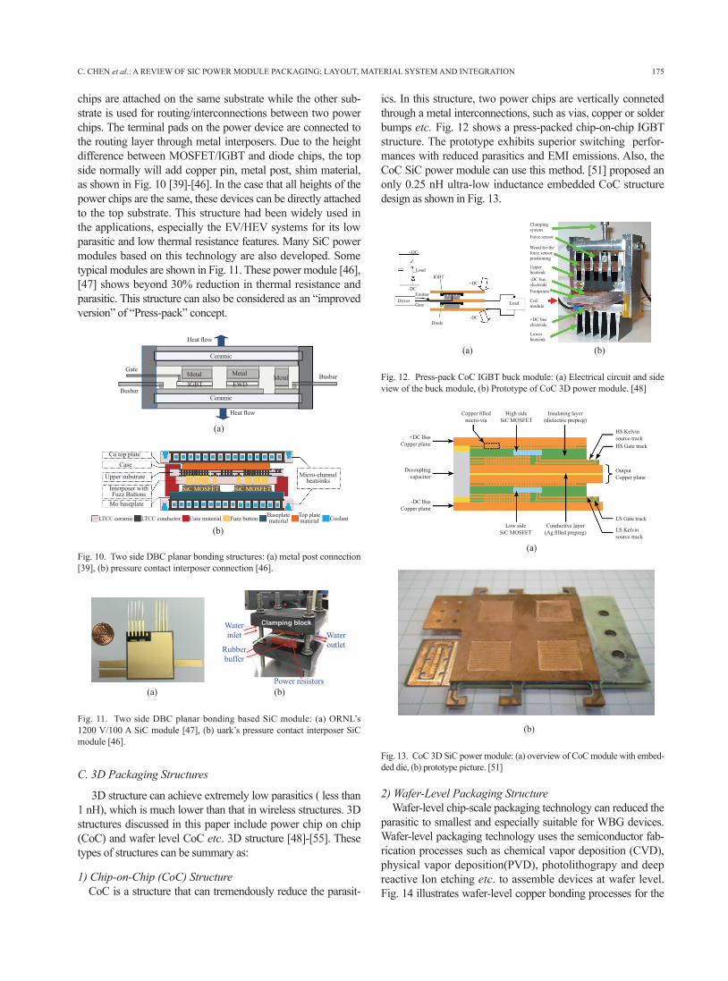
chips are attached on the same substrate while the other sub-strate is used for routing/interconnections between two power chips. The terminal pads on the power device are connected to the routing layer through metal interposers. Due to the height difference between MOSFET/IGBT and diode chips, the top side normally will add copper pin, metal post, shim material, as shown in Fig. 10 [39]-[46]. In the case that all heights of the power chips are the same, these devices can be directly attached to the top substrate. This structure had been widely used in the applications, especially the EV/HEV systems for its low parasitic and low thermal resistance features. Many SiC power modules based on this technology are also developed. Some typical modules are shown in Fig. 11. These power module [46], [47] shows beyond 30% reduction in thermal resistance and parasitic. This structure can also be considered as an “improved version” of “Press-pack” concept.
C. 3D Packaging Structures
3D structure can achieve extremely low parasitics ( less than 1 nH), which is much lower than that in wireless structures. 3D structures discussed in this paper include power chip on chip (CoC) and wafer level CoC etc. 3D structure [48]-[55]. These types of structures can be summary as:
1) Chip-on-Chip (CoC) StructureCoC is a structure that can tremendously reduce the parasit-
ics. In this structure, two power chips are vertically conneted through a metal interconnections, such as vias, copper or solder bumps etc. Fig. 12 shows a press-packed chip-on-chip IGBT structure. The prototype exhibits superior switching perfor-mances with reduced parasitics and EMI emissions. Also, the CoC SiC power module can use this method. [51] proposed an only 0.25 nH ultra-low inductance embedded CoC structure design as shown in Fig. 13.
2) Wafer-Level Packaging StructureWafer-level chip-scale packaging technology can reduced the
parasitic to smallest and especially suitable for WBG devices. Wafer-level packaging technology uses the semiconductor fab-rication processes such as chemical vapor deposition (CVD), physical vapor deposition(PVD), photolithograpy and deep reactive Ion etching etc. to assemble devices at wafer level. Fig. 14 illustrates wafer-level copper bonding processes for the
(a) (b)
Waterinlet
Rubberbuffer
Power resistors
Wateroutlet
Fig. 11. Two side DBC planar bonding based SiC module: (a) ORNL’s 1200 V/100 A SiC module [47], (b) uark’s pressure contact interposer SiC module [46].
(a)
Heat flow
Gate
Busbar
Cu top plate
SiC MOSFET SiC MOSFET
Case
Upper substrate
Mo baseplate
LTCC ceramic LTCC conductor Case material Fuzz button CoolantBaseplatematerial
Top platematerial
Interposer withFuzz Buttons
Micro-channelheatsinks
Ceramic
Ceramic
Heat flow
BusbarMetal MetalMetal
IGBT EWD
(b)
Fig. 10. Two side DBC planar bonding structures: (a) metal post connection [39], (b) pressure contact interposer connection [46].
Fig. 12. Press-pack CoC IGBT buck module: (a) Electrical circuit and side view of the buck module, (b) Prototype of CoC 3D power module. [48]
(a) (b)
ClampingsystemForce sensor
Wood for theforce sensorpositioning
Upperheatsink-DC buselectrodeFootprints
CoCmodule
+DC buselectrode
Lowerheatsink
Load
-DCDiode
DriverEmitter
Gate
-DC
Load
+DC
IGBT+DC
Fig. 13. CoC 3D SiC power module: (a) overview of CoC module with embed-ded die, (b) prototype picture. [51]
(a)
Copper filledmicro-via
Low sideSiC MOSFET
Conductive layer(Ag filled prepreg)
High sideSiC MOSFET
Insulating layer(dielectric prepreg)
HS Kelvinsource trackHS Gate track
OutputCopper plane
LS Gate track
LS Kelvinsource track
+DC BusCopper plane
Decouplingcapacitor
-DC BusCopper plane
(b)
C. CHEN et al.: A REVIEW OF SIC POWER MODULE PACKAGING: LAYOUT, MATERIAL SYSTEM AND INTEGRATION

176 CPSS TRANSACTIONS ON POWER ELECTRONICS AND APPLICATIONS, VOL. 2, NO. 3, SEPTEMBER 2017
direct attachment of high-current copper contact onto Si devices [54]. At module level, high-side and low-side power devices can be vertically interconnected through their metal contacts. Another wafer level packaging concept utilizes the Through
Silicon Vias (TSVs) to connect the gate drive chips and power chips, as shown in Fig. 15 [55]. This approach provides poten-tial solution of wafer-level integration for the gate driver and the power chip. Although these technologies had only been demon-strated in Si power module packaging, they offer attractive and inspiring features to SiC power module.
Iv. pAckAgIng mAterIAl system
The State-of-the-art silicon packaging material systems can operate up to 175ºC which is in compatible with the limits of Si devices. WBG devices, which can operate at much high-er temperatures (200-350ºC) and electric fields (10x than Si devices), requires updated packaging material systems to pro-vide compatible high breakdown voltage strength, compatible thermal-mechanical characteristics for better Coefficient of Thermal Expansion (CTE) matching with SiC material, and the capability of withstanding higher operating temperatures. These challenges mainly characterized to four parts – substrate, die attachment, bonding and encapsulation.
A. Substrate
A power packaging substrate consists of two metal layers and an insulation layer, usually a ceramic layer, in the middle. Different metal and ceramic materials provide different perfor-mances in module packaging. TABLE IV lists a comparison among four normally used ceramic materials [56]-[59]. Among all choices, Al2O3 is the most economic choice but has the high-est thermal impedance and moderate mechanical strength. BeO has the highest thermal conductivity, however, the dust particle formed during its processing is hazardous to health. In com-parison, AlN is a safe material featuring much higher thermal conductivity than Al2O3, and closer CTE matching with SiC materials. Its flexural strength is similar to that of Al2O3, so is its
TABLE IVmAIn thermAl, mechAnIcAl And electrIcAl chArActerIs-
tIcs of cerAmIc suBstrAtes
Si3N4 AlN Al2O3 BeO
Dielectric constant 8~9 8~9 9~10 6-8
Loss factor 2×10⁻⁴ 3×10⁻⁴ 3×10⁻⁴-1×10⁻³ 3×10⁻⁴
Resistivity (Ω∙m) > 1012 > 1012 > 1012 > 1012
Dielectric breakdown strength (kV/mm) 10 - 25 14 - 35 10 - 35 27-31
Thermal conductivity(W/m∙K) 40-90 120-180 20-30 209-330
Bending strength (MPa) 600-900 250-350 300-380 ≥250
Young Module (GPa) 200-300 300-320 300-370 330-400Fracture toughness (MPa∙m1/2) 4-7 2-3 3-5 1-2.5
CTE (mm/m∙K) 2.7-4.5 4.2-7 7-9 7-8.5
Available substrate tech-nologies for thick film metallization
AMB (Cu) DBC (Cu), AMB (Al) DBC (Cu) DBC (Cu)Fig. 15. Gate drive chip on power chip 3D wafer-level packaging structure: (a)
TSV interconnection possibilities between the power device and gate drive, (b) Possible representation of the 3D power module. [55]
(b)
Sourcecontact
Draincontact
Gate signalbonding wires
Verticalpower
MOSFET die
Storagecapacitor
Cmos gatedriver die
(a)
Drain
SourceWire bond interconnectControl signal
Control/driver die
Power device active region
Power device active region
Drain
Drain
Source
Source
Flip Chip +Thermal compression
TSV +Thermal compression
Control/driver die
Control/driver die
Control signal
Control signal
Fig. 14. 3D wafer-level packaging for vertical power devices: (a) wafer level direct bonding processes on a metallic substrate, (b) power module picture. [54]
(a)
(b)
1.Future backsurface process
steps (implantation,annealing)
Si substrate Temporary Sisubstrate
Metallicsubstrate
Si substrate
n+n+
n
np+n+
n-Si
Si diode Si diode Si diode
Metallicsubstrate
2. Direct bondingon temporary
substrate
3. Si mechanicalthinning,
Top surface processsteps
4. Direct metallicbonding
5. Si temporarysubstrate removal

177
thermal cycling lifetime. Si3N4 is a better choice in terms of its much higher thermal cycling reliability, but the penalties are its higher material cost and lower thermal conductivity [60].
According to the differences in manufacturing process, these substrates fall into four major categories: direct bonded copper (DBC) [61], [62], direct bonded aluminum (DBA) [63]-[66], insulated metal baseplate (IMB) [67], [68] and thick film copper (TPC) [69], [70].
1) DBC is widely used in different packaging applications because of its balance between outstanding performances and relatively low cost. DBC is made through high tem-perature process, during which a thin copper-oxide on the copper foil is used to create a eutectic bond between the copper and ceramic. However, the oxidization layer on the bonding interface creates a weak point of delamination, and thus, DBC has moderate life-time in thermal cycling. Active Metal Brazing (AMB) process is another choice to join the metal and the ceramic [61]. Using AMB process can eliminate the oxidization layer, and thus, it can im-prove the life-time of the substrate.
2) DBA has to be mentioned. [63] It uses AlSi-brazing to bond the aluminum and the ceramic. The DBA substrate with the Al alloy base plate is capable of increasing the module reliability in terms of thermal cycling. However, thermal conductivity of DBA is not better than that of DBC. To further improve the thermal conductivity of DBA substrates, lots of variations have been proposed [71]. In these variations, Al is used as a buffer to release the ther-mal-mechanical stresses, and a layer of copper is deployed to enhance the thermal conductivity of the substrate. Fig. 16 shows the combination of these metal layers in new DBA substrate design, which has significant increasing in life-time of their thermal cycling.
Fig. 16. Schematic showing a comparison between three types of module structures and the conventional modules structure. [71]
3) IMB is another good substrate candidate. Since IMB do
not have complexity of fabrications and high temperature treatment as DBC, IMB has lower fabrication cost and long term reliability. It consists of a highly thermal-con-ductive insulating resin sheet, a copper baseplate and thick copper foils. IMB has good heat dissipation while satisfying the isolation requirement. It’s reported in Mit-subishi IGBT module that (Fig. 17), with optimized IMB insulating material and thickness, the module’s life-time in thermal cycling has been enhanced, and the effective chip-mounting area has been increased by 23% [67]. The Samsung used a similar CBMTM substrate [68]. The life time reliability has been extended more compared to the DBC substrate even in extreme test conditions.
Fig. 17. Cross-sectional view of package: (a) conventional ceramic sub-strate and (b) proposed IMB. [67]
4) Another method to form metal bonded ceramic substrates is using TPC [69], [70] technology. Thick layers of copper paste are applied by screen printing process and are fired at 850-950 °C to sinter the metal powders and create a high adhesion bond between the metallic film and the ceramic substrate. This technology provides excellent temperature cycling reliability and opens possibility to combine power and logic components by parallel realization of thin and thick Cu pattern tracks. As shown in Fig. 18, standard DBC substrates on alumina failed before 200 thermal shock cycles (-40 °C, +150 °C), thick print copper sub-strates on alumina show no sign of delamination even after 2000 cycles and thick print copper on aluminum nitride remains stable up to 1800 cycles.
Fig. 18. TPC substrate: (a) 300μm thick printed copper substrate, (b) reli-ability comparison results. [69]
Fig. 19 shows the comparison of above four types of sub-strate, as shown in the DBA, CBM and TPC have the highest reliability. Since the constraint of high temperature isolation material for CBM, it cannot work at high temperature SiC pack-aging. Therefore, DBA derivative types and TPC will be a good candidate for high temperature WBG device packaging.
Conventional type
Solder Cu
Cu Cu
Cu
A1N
A1N A1N
A1N
A1 alloy
A1 alloy A1 alloy
A1
A1
A1 A1
A1
Type 0
Type IIType I
(a)
wirewire
chipchip
Gel
baseplate Solder layers ceramic substrate Solder layerInsulated metal baseplate
DP Resin
(b)
(a)
DBC on Al2O3
Thick Print Copper on AlNThick Print Copper on Al2O3
DBC TPC TPC
Num
ber o
f The
rmal
Sho
ck C
ycle
s
2500
2000
1500
1000
500
0
(b)
C. CHEN et al.: A REVIEW OF SIC POWER MODULE PACKAGING: LAYOUT, MATERIAL SYSTEM AND INTEGRATION

178 CPSS TRANSACTIONS ON POWER ELECTRONICS AND APPLICATIONS, VOL. 2, NO. 3, SEPTEMBER 2017
Fig. 19. Comparison of different types of substrates.
B. Die-Attaching Materials
Die-attaching materials fall into many categories, spanning both high and low temperature use. The five main categories are (1) epoxy adhesives, (2) alternative resins, (3) eutectic die attach solders, (4) soft soldering and (5) silver-glass material [72]. Two of the most commonly used die-attach materials to-day are solder alloys and conductive epoxy. Most silver filled epoxies used in commercial small-signal devices fail at tem-peratures near 200 °C. Their low operational temperatures are not workable solutions for high temperature applications. Alter-native resins with the use of organic compounds are applicable also to low power Si devices.
Beyond 200 ºC, [72] had summarized the existing die attach-ing materials as shown in Fig. 20. In the low temperature range 200~300 ºC, the tin-lead (Pb-Sn) and lead-free tin-silver-copper (SAC) alloy solder are listed in the figure. As we can see in the middle range 300~400 ºC, the tin-lead (Sn-Pb) solder systems
have high liquidus points and they have been popular for high temperature die attach materials thus far.
However, the higher the Pb content, the slower the through-put in automated die attach machines, due to the time required for the Pb-Sn liquid to re-solidify after the die attach operation is completed, causing voiding in between the die and substrates’ crevice. For larger dies, which require more die attach material coverage, the voiding issue will be more pronounced. Addition-ally, since the ban on hazardous materials in consumer electron-ics since 2006, and beyond consumer electronics in the whole electronics industry nowadays, the Pb solder are forbidden [73].Hence, the lead-free high temperature solder are emergency technology. It is worth noting that lead-free silver sintering, dif-fusion soldering and reactive multilayer bonding are emerging die attach technologies with the potential to provide improved chip to substrate interconnection in terms of mechanical, elec-trical, high temperature and thermal performance [74]-[78]. As depicted in the high temperature range in the figure, these sol-ders have very high liquidus temperature.
Silver sintering is also known as low temperature joining technique (LTJT). The process is based on the spontaneous sinter ability of silver particles in the nano and micro scale with applied pressure at temperatures of above 220 °C [79]-[85]. Silver sintered interconnections show numerous advantages such as a remarkable high melting point of 961 °C, a far better thermal conductivity (250 W/mK) and an enhanced electrical conductivity (41 MS/m). In addition to the positive mechanical characteristics, such as a CTE value of 19 μm/mK and a good tensile strength of 55 MPa, they show considerably enhanced reliability in thermal and power cycling tests. Today, silver sin-
Fig. 20. Various die attach materials and solders, their operating range and application possibilities. [72]
ThermalPerformance
Ease ofFabrication
Reliability GoodFairPoor
GoodFairPoor
GoodFairPoor
DBC DBA DBAType I
DBAType II
CBM/IMB TPC
*Liquidus temperature as governing limit
Various applications possible across industries
Sensors and electronics
Sensors andelectronics
Sensors andelectronics
ExplorationManufacturingindustry
Space SpaceAvionics
Automotive Automotive Automotive
High range (≥500 °C)Medium range (300-400 °C)Low range (200-300 °C)
Pb98-Sn1.2-Ga0.8Pb91-Sn4-Ag4-In1
Pb-Sb1.5Pb-Sb2
Pb-In575Pb-25InPb92.5-In5-Ag2.5
Pb92.86-In4.76-Ag238Pb-Sn10.5
100PbPb-2.5Ag
Sn-Ag25-Sb10 Sn-Pb98
Sn-Ag3.1-In10Sn-Ag3-Cu0.5-In10
Sn-Ag3.4-Bi4.8Sn-Ag3.5-Cu0.9
Sn-Ag3.8-Cu0.7Sn-Ag3.9-Cu0.6
Sn-Ag4-Cu0.5
Sn-Pb15-Te0.5-P0.1
Sn-Ag3-Cu0.5
Sn-3.3Ag-2CuSn-Cu0.7
96.5Sn-3.5Ag
50Pb-50In
Die
atta
ch m
ater
ials
& so
lder
s by
max
imum
* O
pera
ting
tem
pera
ture
s
Sn-5Sb
Sn-Pb70Sn-Pb65
Pb-Sn2-Ag2.5Sn-(1-4)-Cu
Zn-(4-6)A1(-Ga, Ge, Mg, Cu)
Au100
Au-2Si
Au-Ni18
Au thermo-compression bonding
Au thick film paste
A1-Sil1.7
Silver-Indium
Sintered nano-Silver
Pb-Sn5-Ag2.5
Sn-Pb80 Pb-Sn5
Pb-In5-Ag5
Pb-Sn1-Ag1.5Pb-In19 Bib-Ag11-Ge0.5
Bi-2.5Ag-0.2Cu Au88-Ge12Pb-Sn10-Ag2
Au80-Sn20Pb90-Ag5-Sn5
Sn-25Ag-10SbPb-Sn3-In2-Ag2
55Ge-45A1 Au-In25Au-In18
Pb-Sn10 Zn-(10-30)-Sn
Au-3.24Si

179
tering is applied during industrial manufacturing for a range of selected products but has not been introduced as a flexible and versatile technology platform into mass manufacturing. The root cause for the current situation is that quality issues and fail-ures in silver-sintered contact interfaces in dependence of chip and substrate metallization, as well as variations in the sintering process, are not understood in detail and will be the aim of fur-ther research.
Diffusion soldering describes an interconnection technol-ogy based on a metal interlayer where solid-solid as well as liquid-solid diffusion between joining materials is stimulated. Transient Liquid Phase Bonding (TLPB) realized by bonding of parent materials with pre-deposited low-melting metal layer, whereas Transient Liquid Phase Soldering (TLPS) involves usage of the printed standard soft solders as interlayer for inter-metallic phase (IMP) formation [77], [86]-[89]. The diffusion solder have Ag/In [90], [91], Ag/Sn [92], Au/In [93], [94], Au/Sn [95], [96], Cu/Sn [97], [98], and Ni/Sn [99]. Considered the cost and environment friendly, the Cu-Sn alloy solder has been a good candidate for high temperature applications. Because of lack of the understanding of physical principle, characterization and soldering processes, the use of these materials are not well known.
In summary, the presented new concept joining technologies show remarkable properties with the potential to improve the quality of power electronic packaging. Hence, knowledge of specific quality and reliability-affecting factors, as well as the availability of adequate testing methods for a detailed charac-terization of the formed metallic joints, are necessary in order to assure a high strength and a long term reliability of silver sin-tered, diffusion soldered or reactive bonded devices.
C. Bonding Methods
Copper wire bonding (Fig. 21(a)) is one of the most promis-ing technologies for connecting high current interconnections in power electronics assemblies [76], [100]. The high flexibility in the layout and established quality from the aluminum wire bonding process are two reasons to promote the development
of Cu wire bonding. Using copper material over aluminum for wire bond interconnections provides two key benefits such as, increase in current capacity by 37% and the excellent thermal conductivity of copper (~80% better compared to Al). Recently, novel heavy wire bonds made of an Al and Cu composite ma-terial [101] were introduced as shown in Fig. 21(b). In contrast to a pure Cu-wire no change in the metallization of the chip sur-face is necessary to establish a stable bonding process. The new material is still under development with the goal to increase the Cu content to a maximum without yield problems during the bonding process.
Fig. 21. Novel wire-bonding: (a) Cu wire-bonding [76], (b) Cu-Al wire bonding [101].
Another bonding method should be noted is Cu and Al rib-bon bonding [100], [102], [103] as shown in Fig. 22. Due to the lower number of ribbons required to achieve the same intercon-nect resistance as for wire bond interconnects. These connec-tions can carry higher currents and show better power cycling capabilities in dependence of the respective bonding process and the chosen ribbon material. Al or Cu ribbon bonding is an attractive new interconnection solution for the replacement of wire bonds between the power semiconductor and the substrate.
Fig. 22. Ribbon bonding: (a) Al ribbon [100], (b) Cu ribbon [102].
TABLE VsummArIes cAndIdAtes for hIgh voltAge encApsulAtIon
Material Part Number Manufacturer Dielectric Constant Breakdown strength Temperature Range (ºC)
Dielectric Fluid Novec® 7500 3M 5.8 35 kV, 0.1” gap 128 max.
Polyamide Imide (PAI) Torlon® 4203 Boedeker Plastics 4.2 (@ 1 MHz) 100 – 280 kV/mm 260 max.
Epoxy Hysol® -60NC Henkel 21.7 550 V/mil -
Silicone 3-6635 Dow Corning 20.5 20 kV/mm -80 to 200
Silicone Sylgard® 567 Dow Corning 2.79 (@ 100 kHz) 16 kV/mm -45 to 200
Silicone TSE3051 Momentive 2.8 18 kV/mm -
Silicone CF2186 Nusil 35.4 19.5 kV/ mm -140 to 315
Silicone R-2188 Nusil 2.6 (@ 100 kHz) 500 V/mil 19.5 kV/mm -
Benzocyclobutene (BCB) Dow Chemicals 2.65 530 kV/mm
(a) (b)
(a) (b)
C. CHEN et al.: A REVIEW OF SIC POWER MODULE PACKAGING: LAYOUT, MATERIAL SYSTEM AND INTEGRATION

180 CPSS TRANSACTIONS ON POWER ELECTRONICS AND APPLICATIONS, VOL. 2, NO. 3, SEPTEMBER 2017
D. Encapsulation
Encapsulation materials protect the power module compo-nents from external environmental damages, such as moisture, solvents, gases, and radiations [104], [105]. In addition, encap-sulation materials improve the voltage ratings of the packages, in high voltages modules (>1000 V) and prevent arcing between different electrodes. However, the soft conventional encapsula-tion materials mainly designed for Si conventional module are limited to low temperature of about 200 °C. Therefore, identify-ing new materials for higher temperature application is manda-tory.
Without considering hermetic packaging where gases, vacu-um and liquids can be used as dielectrics, three types of materi-als might be suitable for high-voltage high-temperature power electronic packaging; glasses, hydroset ceramics and polymers. The main drawbacks of glasses are they have high firing tem-peratures more than 500 °C and they have high Young modulus causing high thermo-mechanical stresses.
In contrast, hydroset ceramics offer low curing temperature (curing can be realized at room temperature). However, those ceramics get a high Young modulus (>100 GPa) and a coeffi-cient of thermal expansion (CTE) between 3 and 6 ppm/°C that can induce high stresses in the structure. The CTE mismatch materials can lead to severe reliability problem.
Polymeric encapsulation is the third type of materials and can be divided into two categories: soft and hard encapsulation. Soft encapsulation materials exhibit a very low Young modulus in order of several MPa and a high CTE. Silicone gels belongs to this kind of polymers and are widely retained for encapsulating high voltage multi-chip power assemblies, due to their very high softness and high insulating electrical properties. However, the literature review shows that high temperature commercially available silicone gels exhibit a maximum temperature limit lower than 250 °C for continuous service of operation [57], [106]. The review also reveals that a trade-off between high temperature ability and softness of silicones generally exists. In fact, a slight extension of the temperature range (up to 250 °C - 275 °C) might be obtained with the use of silicone elastomers.
In the second category, polymers are relatively hard and ex-hibit a low CTE and a relatively high Young modulus (several GPa). The reliability of some of the second category polymers (like polyimide BPDA-PDA and PA-HT), tested at temperature exceeding the 300 °C seems satisfactory [107]. However, the deposition technique of the former and the limited thickness (50 μm) of the latter (deposited by polymer vapor deposition) reduce their use at the wafer level.
Other polymers, like benzocyclobutene BCB are candidates and are stable at the temperature above 300 °C, but the major issue encountered for thick films is the void generation during the curing process [108].
In response to the high-voltage/ high electrical-field feature in SiC modules, encapsulation material with high breakdown voltage is also important to the packaging system. Off-shelf choices for these materials include silicone Gels, PAI materials
and BCB materials. TABLE V summaries candidates for high voltage encapsulation [109]-[115].
v. sIc module IntegrAtIon
SiC devices is capable of high switching speed and high-tem-perature operation, yet it is sensitive to the packaging parasitics. Using advanced structure can significantly help with this prob-lem. Integrating power devices with its associate components, structurally and functionally, is another way to solve this puzzle.
Module-level integration integrates associated components, such as decoupling capacitors, gate drivers, temperature sensors, current sensors and protection circuits, in the same package. This idea has been proven to be capable of further mitigating the influences from packaging parasitics. It is a good approach to improve the density and efficiency of power electronics converters [25]-[27], [51], [116]-[123]. The Intelligence Power Module (IPM) is one of the successful products which demon-strate this concept. SiC module may require a higher level of functional and structural integration trimmed for the new char-acteristics of the device [27], [51], [53], [55], [121], [122], [124].
A. Integration of Decoupling Capacitor
References [24]-[28], [51] described a solution that embed-ded discrete Multilayer Ceramic Capacitor (MLCC) decoupling capacitors in the SiC modules, as shown in Fig. 13. This inte-gration approach can significantly reduce the distance between power device pair and the decoupling capacitors, and thus reduces power loop parasitics, suppresses the voltage overshoot and improves current sharing among paralleled devices. This method can achieve clean switching waveforms, low elec-tromagnetic interference, and higher power efficiency at high switching speed.
B. Integration of Gate Driver
Integrating gate drives with the power chip in the module can tremendously reduce the gate driving loop inductance and improve the driving performances. Using Silicon-on-Insula-tor (SOI) technology or SiC low voltage device technology, high-temperature gate driver integration can be realized in SiC modules.
Fig. 23 illustrates an integrated design from SEMIKON that SOI gate driver ICs is directly mounted on the DBC substrate in
(a)
IGBThalf bridge
Temperature SensorSiC MOSFETs
SiC Gate Drivers
1200V SOIhalf bridgegate driver
(b)
Fig. 23. Integration of decoupling capacitor and gate driver: (a) SOI gate driver integration in IGBT power module [126], (b) decoupling capacitor and SOI gate driver integration in SiC power module [119].

181
a 1200 V IGBT half-bridge MiniSKiiP module [125], [126] and demonstrated significant improvement in the module switching performance. The University of Arkansas had developed a SiC half-bridge switching module with integrated SiC gate drivers and dc-decoupling capacitors [119], [127]. The integrated gate drivers require no gate-damping resistance because of the ex-trememly low parasitic gate inductance.
C. Integration of EMI Filters
Increasing switching speed is usually an advantage from the thermal and efficiency points of view, yet it has detrimental ef-fects on the EMI emission. The “side-effects” of fast switching is that SiC module may generate too much EMI noises, and thus, a more bulky EMI filter is required at the converter level. Integrating EMI filters in SiC module and “self-containing” the noises within the module is a promising approach from convert-er design point of view. References [123], [128] provide a solu-tion to directly integrate the CM filter capacitors in the power module, as shown in Fig. 24. This makes it possible to “capture” the high-frequency harmonics directly at the source.
Fig. 24. The power module with integrated common mode filtering: (a) SiC-JFET power module prototype with integrated CM capacitors, (b) EMI spectrum comparison between with and without integration. [123]
D. Integration of Sensor
Integrated sensors are often present in Si- IGBTs [129] or power modules like in Infineon’s MIPAQ family, providing valuable information, which can be used either for monitoring, failure mitigation or studying the device aging. It is then obvi-ous that such information is valuable for SiC-MOSFETs as they begin to be integrated into power systems.
Temperature and current sensors can be integrated into the package separated from the main device; in this case, providing information on the package temperature and device current. However, this type of method cannot react fast and the addi-tional current sensor will increase the loop distance. The sensor integrated in the SiC-MOSFET active area by monolithic in-
tegration technology will be an emerging technology to solve it. This can provide a more precise temperature measurement in the device itself, allowing fast reaction in case of failure and more accurate information. As shown in Fig. 25, [124] proposed a SiC MOSFET with monolithic integrated sensor.
E. Integration of Thermal Management System
In a SiC power module, the heat-sink can be integrated with the baseplate or with the DBC. This integration strcture can sig-nificantly reduce the thermal impedance in the module through eleminating thermal-interfaces between the SiC device die and the ambient. Nowadays, the pin-fin baseplate power module [130]-[133] is widely used in automotive applications. The power module described in reference [130]-[133] integrated pin-fin on the baseplate and can be directly mounted on a liquid cold plate. Fig. 26(a) shows the new Mitsubishi J1-Series pin-fin integrated IGBT module, which demostrate a 76% weight reduction and 30% thermal performance improvement for three phase inverter solutions. Fig. 26(b) shows a pin-fin integrated, double-sided cooled, SiC module design from ORNL [47] , which achieves a 40% reduction in thermal resistance.
Fig. 26 Pin-fin integrated power module: (a) Mitsubishi J1-Series IGBT module [130], (b) SiC pin-fin double sided cooling module [47].
(b) (a)
Cooling fin
(a)Integrated CM Capacitors Frequency (Hz)
100k 1M 10M
100
90
80
70
60
50
40
30
20
Vcm
(dBμ
V)
SiC-JFETw/o Ccm 1Ccm 1=6 nF
10 mm
(b)
(a) (b)
Fig. 25. Monolithic integrated sensor in SiC MOSFET: (a) schematic of cross-section, (b) SEM picture of fabricated 2.25 mm2 SiC power MOSFET with monolithically integrated temperature and current sensors. [124]
PWell PWell PWellN-Type
PWell
Bulk
Currentsensor
Gate Source
TemperatureSensor
Gate
Drain
GateGate
Source Contact Source Contact
Drift Layer
Temperature Sensor
Fig. 27. Full SiC power module with cooling sintering on substrate: (a) top view, (b) side view. [134]
(a)
(b)
C. CHEN et al.: A REVIEW OF SIC POWER MODULE PACKAGING: LAYOUT, MATERIAL SYSTEM AND INTEGRATION

182 CPSS TRANSACTIONS ON POWER ELECTRONICS AND APPLICATIONS, VOL. 2, NO. 3, SEPTEMBER 2017
However, the mechanical assembly and the liquid sealing for the pin-fin module is a weak point in the system, and a threaten to the life-time of the module. An alternative approach is to sinter the ceramic substrate directly onto a sealing-free heatsink such as a microchannel copper cooler [134]. This combination offers a very low thermal path between substrate and cooling liquid. Fig. 27 shows a SiC power module [134] with ceram-ic substrate directly sintering on a sealing-free heatsink mi-cro-channel copper cooler.
vI. conclusIon
This paper provides overview for the state-of-the-art packag-ing technologies for SiC power modules. The paper covers the information regarding off-shelf SiC devices and the advanced packaging technologies from on-going research efforts. The pa-per summarizes these research advancements for SiC modules from three aspects: (1) module layout and structures, (2) new packaging material systems, and (3) module integration trend.
According to existing literatures, the focal points of on-going SiC module research include: (a) parasitic inductance mini-mization for power loop and gate loop, (b) high temperature operation design and (c) module integration to further optimize SiC switching operation with EMI noises self-containment and better thermal management. Most of the new packaging layouts, structures and integration schemes are developed for reducing the influences from package parasitics and side-effects of fast switching. The packaging materials system for SiC de-vice is more determined by its nature of high temperature/high electric-field operation. The design trade-off is typically in ther-mal-mechanical-electrical multi-physics domain. Integration is an important trend for SiC devices as it provides numerous benefits for SiC switching operation. All these new approaches are for the purpose of unleashing the intrinsic benefits from SiC devices in its applications to achieve higher power density and efficiency over Si-based power conversion. It is clear that, duplicating Si packaging technologies and “dropping-in” SiC device will not have desire performance output that matches to SiC characteristics. New packaging architecture trimmed for SiC is required for future power electronics systems.
Thermal management is another important topic for SiC packaging, yet its content is relatively independent to the device itself and worth another paper dedicate on this topic.
AcknoWledgment
The authors would like to express their appreciations to Mr. Amol Deshpande and Mr.Yingzhuo Chen for their helps in col-lecting literatures in related areas.
references
[1] J. A. Cooper, M. R. Melloch, R. Singh, A. Agarwal, and J. W. Pal-mour, “Status and prospects for SiC power MOSFETs,” IEEE Trans-actions on Electron Devices, vol. 49, no. 4, pp. 658-664, 2002.
[2] M. N. Yoder, “Wide bandgap semiconductor materials and devices,” IEEE Transactions on Electron Devices, vol. 43, no. 10, pp. 1633-1636, 1996.
[3] A. Elasser and T. P. Chow, “Silicon carbide benefits and advantag-es for power electronics circuits and systems,” Proceedings of the IEEE, vol. 90, no. 6, pp. 969-986, 2002.
[4] B. Ozpineci and L. Tolbert, Comparison of wide-bandgap semicon-ductors for power electronics applications. United States. Depart-ment of Energy, 2004.
[5] R. M. Burkart and J. W. Kolar, “Comparative evaluation of SiC and Si PV inverter systems based on power density and efficiency as in-dicators of initial cost and operating revenue,” in Control and Mod-eling for Power Electronics (COMPEL), 2013 IEEE 14th Workshop on, IEEE, 2013, pp. 1-6.
[6] T. Daranagama, N. Udugampola, R. McMahon, and F. Udrea, “Comparative analysis of static and switching performance of 1.2 kV commercial SiC transistors for high power density applications,” in Wide Bandgap Power Devices and Applications (WiPDA), 2013 IEEE Workshop on, IEEE, 2013, pp. 48-51.
[7] B. Whitaker et al., “A high-density, high-efficiency, isolated on-board vehicle battery charger utilizing silicon carbide power devic-es,” IEEE Transactions on Power Electronics, vol. 29, no. 5, pp. 2606-2617, 2014.
[8] S. Ji, D. Reusch, and F. C. Lee, “High frequency high power density 3D integrated gallium nitride based point of load module,” in 2012 IEEE Energy Conversion Congress and Exposition (ECCE), IEEE, 2012, pp. 4267-4273.
[9] S. Araujo, M. Kazanbas, M. Wendt, T. Kleeb, and P. Zacharias, “Prospects of GaN devices in automotive electrification,” in PCIM Europe 2014; International Exhibition and Conference for Power Electronics, Intelligent Motion, Renewable Energy and Energy Man-agement; Proceedings of, VDE, 2014, pp. 1-8.
[10] B. Passmore et al., “Wide bandgap packaging for next generation power conversion systems,” in 2013 4th IEEE International Sym-posium on Power Electronics for Distributed Generation Systems (PEDG), IEEE, 2013, pp. 1-5.
[11] S. Tiwari, O. -M. Midtgård, and T. M. Undeland, “Comparative evaluation of a commercially available 1.2 kV SiC MOSFET mod-ule and a 1.2 kV Si IGBT module,” in Industrial Electronics Society, IECON 2016-42nd Annual Conference of the IEEE, IEEE, 2016, pp. 1093-1098.
[12] [Online].Available: http://www.wolfspeed.com/power/products/sic-mosfets/table.
[13] [Online].Available: http://unitedsic.com/cascodes/. [14] [Online].Available: http://unitedsic.com/sic-jfets/. [15] [Online].Available: http://www.rohm.com/web/global/search/para-
metric/-/search/SiC%20MOSFET. [16] [Online].Available: http://www.st.com/content/st_com/en/products/
sic-devices/sic-mosfets.html?querycriteria=productId=SC2162. [17] Z. Chen, “Characterization and modeling of high-switching-speed
behavior of SiC active devices,” 2009. [18] [Online].Available: http://www.wolfspeed.com/power/products/
sic-power-modules/table. [19] [Online].Available: http://www.rohm.com/web/global/full-sic-pow-
er-modules. [20] [Online].Available: http://www.genesicsemi.com/commercial-sic/
sic-modules-copack/. [21] [Online].Available: https://www.infineon.com/cms/en/product/pow-
er/sicarbide-sic/coolsic-mosfets/channel.html?channel=5546d4625c-167129015c39e6eae53065.
[22] [Online].Available: https://www.semikron.com/products/prod-uct-classes/sic/full-sic.html.
[23] R. Bayerer and D. Domes, “Power circuit design for clean switch-ing,” in Integrated Power Electronics Systems (CIPS), 2010 6th International Conference on, IEEE, 2010, pp. 1-6.
[24] Z. Chen, Y. Yao, D. Boroyevich, K. D. Ngo, P. Mattavelli, and K. Rajashekara, “A 1200-V, 60-A SiC MOSFET multichip phase-leg module for high-temperature, high-frequency applications,” IEEE Transactions on Power Electronics, vol. 29, no. 5, pp. 2307-2320, 2014.
[25] M. Wang, F. Luo, and L. Xu, “A double-end sourced multi-chip im-proved wire-bonded SiC MOSFET power module design,” in 2016 IEEE Applied Power Electronics Conference and Exposition (APEC), IEEE, 2016, pp. 709-714.

183
[26] Z. Chen, Y. Yao, D. Boroyevich, K. Ngo, and W. Zhang, “An ul-tra-fast SiC phase-leg module in modified hybrid packaging struc-ture,” in 2014 IEEE Energy Conversion Congress and Exposition (ECCE), IEEE, 2014, pp. 2880-2886.
[27] C. Chen, Y. Chen, Y. Li, Z. Huang, T. Liu, and Y. Kang, “A SiC-based half-bridge module with improved hybrid packaging method for high power density applications,” IEEE Transactions on Indus-trial Electronics, vol. PP, no. 99, p. 1, 2017.
[28] R. Wang et al., “A high-temperature SiC three-phase AC-DC con-verter design for> 100oC ambient temperature,” IEEE Transactions on Power Electronics, vol. 28, no. 1, pp. 555-572, 2013.
[29] A. Narazaki et al., “Direct beam lead bonding for trench MOSFET & CSTBT,” in Proceedings. ISPSD '05. The 17th International Sym-posium on Power Semiconductor Devices and ICs, 2005, 2005, pp. 75-78.
[30] J. F. Donlon, Eric R. Motto, “Transfer molded IGBT module for electric vehicle propulsion,” in Motor, Drive & Automation Systems, 2012.
[31] V. Temple, J. Waldron, J. Azotea, M. Francois, and R. Rodrigues, “High frequency SiC majority carrier modules,” in PCIM Europe 2015; International Exhibition and Conference for Power Electron-ics, Intelligent Motion, Renewable Energy and Energy Management; Proceedings of, VDE, 2015, pp. 1-7.
[32] T. Stockmeier, P. Beckedahl, C. Goebl, and T. Malzer, “SKiN: Dou-ble side sintering technology for new packages,” in 2011 IEEE 23rd International Symposium on Power Semiconductor Devices and ICs, IEEE, 2011, pp. 324-327.
[33] P. Beckedahl, S. Buetow, A. Maul, M. Roeblitz, and M. Spang, “400 A, 1200 V SiC power module with 1nH commutation inductance,” in CIPS 2016; 9th International Conference on Integrated Power Electronics Systems; Proceedings of, VDE, 2016, pp. 1-6.
[34] L. Boettcher, S. Karaszkiewicz, D. Manessis, and A. Ostmann, “De-velopment of embedded power electronics modules,” in Electronic System-Integration Technology Conference (ESTC), 2012 4th, IEEE, 2012, pp. 1-6.
[35] A. Ostmann, L. Boettcher, D. Manessis, S. Karaszkiewicz, and K.-D. Lang, “Power modules with embedded components,” in Micro-electronics Packaging Conference (EMPC), 2013 European, IEEE, 2013, pp. 1-4.
[36] J. Yin, Z. Liang, and J. D. van Wyk, “High temperature embedded SiC chip module (ECM) for power electronics applications,” IEEE transactions on power electronics, vol. 22, no. 2, pp. 392-398, 2007.
[37] K. Weidner, M. Kaspar, and N. Seliger, “Planar interconnect technol-ogy for Power module system integration,” in 2012 7th International Conference on Integrated Power Electronics Systems (CIPS), IEEE, 2012, pp. 1-5.
[38] S. Liebig, J. Engstler, K. Kriegel, and K. Weidner, “Evaluation of enhanced power modules with planar interconnection technology for aerospace application,” in PCIM Europe 2014; International Ex-hibition and Conference for Power Electronics, Intelligent Motion, Renewable Energy and Energy Management; Proceedings of, VDE, 2014, pp. 1-5.
[39] C. Gillot, C. Schaeffer, C. Massit, and L. Meysenc, “Double-sided cooling for high power IGBT modules using flip chip technology,” IEEE Transactions on components and packaging technologies, vol. 24, no. 4, pp. 698-704, 2001.
[40] X. Cao, G.-Q. Lu, and K. D. Ngo, “Planar power module with low thermal impedance and low thermomechanical stress,” IEEE Trans-actions on Components, Packaging and Manufacturing Technology, vol. 2, no. 8, pp. 1247-1259, 2012.
[41] Z. Liang, P. Ning, F. Wang, and L. Marlino, “Reducing parasitic electrical parameters with a planar interconnection packaging struc-ture,” in 2012 7th International Conference on Integrated Power Electronics Systems (CIPS), IEEE, 2012, pp. 1-6.
[42] Z. Liang, P. Ning, F. Wang, and L. Marlino, “A phase-leg power module packaged with optimized planar interconnections and inte-grated double-sided cooling,” IEEE Journal of Emerging and Select-ed Topics in Power Electronics, vol. 2, no. 3, pp. 443-450, 2014.
[43] S. W. Yoon, K. Shiozaki, and T. Kato, “Double-sided nickel-tin tran-sient liquid phase bonding for double-sided cooling,” in 2014 IEEE Applied Power Electronics Conference and Exposition-APEC 2014,
IEEE, 2014, pp. 527-530. [44] A. Grassmann et al., “Double sided cooled module concept for high
power density in HEV applications,” in PCIM Europe 2015; Interna-tional Exhibition and Conference for Power Electronics, Intelligent Motion, Renewable Energy and Energy Management; Proceedings of, VDE, 2015, pp. 1-7.
[45] Y. Wang, Y. Li, X. Dai, S. Zhu, S. Jones, and G. Liu, “Thermal de-sign of a dual sided cooled power semiconductor module for hybrid and electric vehicles,” in Applied Power Electronics Conference and Exposition (APEC), 2017 IEEE, IEEE, 2017, pp. 3068-3071.
[46] N. Zhu, H. A. Mantooth, D. Xu, M. Chen, and M. D. Glover, “A Solution to Press-Pack Packaging of SiC MOSFETs,” IEEE Trans-actions on Industrial Electronics, 2017.
[47] Z. Liang, “Integrated double sided cooling packaging of planar SiC power modules,” in 2015 IEEE Energy Conversion Congress and Exposition (ECCE), IEEE, 2015, pp. 4907-4912.
[48] E. Vagnon, P. -O. Jeannin, J. -C. Crebier, and Y. Avenas, “A bus-bar-like power module based on three-dimensional power-chip-on-chip hybrid integration,” IEEE Transactions on Industry Applications, vol. 46, no. 5, pp. 2046-2055, 2010.
[49] E. Vagnon, J.-C. Crébier, Y. Avenas, and P.-O. Jeannin, “Study and realization of a low force 3D press-pack power module,” in 2008 IEEE Power Electronics Specialists Conference, IEEE, 2008, pp. 1048-1054.
[50] M. Mermet-Guyennet, A. Castellazzi, P. Lasserre, and J. Saiz, “3D integration of power semiconductor devices based on surface bump technology,” in Integrated Power Systems (CIPS), 2008 5th Interna-tional Conference on, VDE, 2008, pp. 1-6.
[51] G. Regnat et al., “Silicon carbide power chip on chip module based on embedded die technology with paralleled dies,” in 2015 IEEE Energy Conversion Congress and Exposition (ECCE), IEEE, 2015, pp. 4913-4919.
[52] J. A. Herbsommer, J. Noquil, O. Lopez, and D. Jauregui, “Innovative 3D integration of Power MOSFETs for synchronous Buck con-verters,” in Applied Power Electronics Conference and Exposition (APEC), 2011 Twenty-Sixth Annual IEEE, IEEE, 2011, pp. 1273-1274.
[53] N. Rouger et al., “True 3D packaging solution for stacked vertical power devices,” in 2013 25th International Symposium on Power Semiconductor Devices & IC's (ISPSD), IEEE, 2013, pp. 97-100.
[54] N. Rouger et al., “3D Packaging for vertical power devices,” in In-tegrated Power Systems (CIPS), 2014 8th International Conference on, VDE, 2014, pp. 1-6.
[55] T. Simonot, J. -C. Crébier, N. Rouger, and V. Gaude, “3D hybrid integration and functional interconnection of a power transistor and its gate driver,” in 2010 IEEE Energy Conversion Congress and Ex-position, IEEE, 2010, pp. 1268-1274.
[56] S. Diaham, M.-L. Locatelli, and Z. Valdez-Nava, Dielectrics for high temperature SiC device insulation: Review of new polymeric and ceramic materials. INTECH Open Access Publisher, 2011.
[57] R. Khazaka, L. Mendizabal, D. Henry, and R. Hanna, “Survey of high-temperature reliability of power electronics packaging compo-nents,” IEEE Transactions on Power Electronics, vol. 30, no. 5, pp. 2456-2464, 2015.
[58] L. Coppola, D. Huff, F. Wang, R. Burgos, and D. Boroyevich, “Sur-vey on high-temperature packaging materials for SiC-based power electronics modules,” in 2007 IEEE Power Electronics Specialists Conference, IEEE, 2007, pp. 2234-2240.
[59] W. Brokaw, J. Elmes, B. Grummel, Z. J. Shen, and T. X. Wu, “Silicon carbide high-temperature packaging module fabrication,” in Wide Bandgap Power Devices and Applications (WiPDA), 2013 IEEE Workshop on, IEEE, 2013, pp. 178-181.
[60] W. W. Sheng and R. P. Colino, Power electronic modules: design and manufacture. CRC press, 2004.
[61] J. Schulz-Harder and K. Exel, “Recent developments of direct bonded copper (DBC) substrates for power modules,” in Electronic Packaging Technology Proceedings, 2003. ICEPT 2003. Fifth Inter-national Conference on, IEEE, 2003, pp. 491-496.
[62] J. Schulz-Harder, “Advanced DBC (direct bonded copper) substrates for high power and high voltage electronics,” in Twenty-Second An-nual IEEE Semiconductor Thermal Measurement And Management
C. CHEN et al.: A REVIEW OF SIC POWER MODULE PACKAGING: LAYOUT, MATERIAL SYSTEM AND INTEGRATION

184 CPSS TRANSACTIONS ON POWER ELECTRONICS AND APPLICATIONS, VOL. 2, NO. 3, SEPTEMBER 2017
Symposium, IEEE, 2006, pp. 230-231. [63] A. Lindemann and G. Strauch, “Properties of direct aluminum bond-
ed substrates for power semiconductor components,” IEEE transac-tions on power electronics, vol. 22, no. 2, pp. 384-391, 2007.
[64] T. G. Lei, J. N. Calata, K. D. Ngo, and G.-Q. Lu, “Effects of large-temperature cycling range on direct bond aluminum substrate,” IEEE Transactions on Device and Materials Reliability, vol. 9, no. 4, pp. 563-568, 2009.
[65] Y. Kuromitsu et al., “Direct bonded aluminum on aluminum nitride substrates via a transient liquid phase and its application,” in Inte-grated Power Electronics Systems (CIPS), 2010 6th International Conference on, IEEE, 2010, pp. 1-5.
[66] S. Kraft, A. Schletz, and M. März, “Reliability of silver sintering on DBC and DBA substrates for power electronic applications,” in 2012 7th International Conference on Integrated Power Electronics Systems (CIPS), IEEE, 2012, pp. 1-6.
[67] K. Ohara, H. Masumoto, T. Takahashi, M. Matsumoto, and Y. Ot-subo, “A New IGBT Module with Insulated Metal Baseplate (IMB) and 7th Generation Chips,” in PCIM Europe 2015; International Ex-hibition and Conference for Power Electronics, Intelligent Motion, Renewable Energy and Energy Management; Proceedings of, VDE, 2015, pp. 1-4.
[68] K.-S. Kim et al., “Novel substrate technology for IPM (intelligent power module) applications: Structural, thermal and electrical char-acteristics,” in Electronic Materials and Packaging (EMAP), 2012 14th International Conference on, IEEE, 2012, pp. 1-3.
[69] P. Gundel et al., “Thick printed copper as highly reliable substrate technology for power electronics,” in PCIM Europe 2015; Interna-tional Exhibition and Conference for Power Electronics, Intelligent Motion, Renewable Energy and Energy Management; Proceedings of, VDE, 2015, pp. 1-6.
[70] Heraeus. Inorganic Substrates for Power Electronics Applications [Online].
[71] N. Terasaki, Y. Nagatomo, T. Nagase, and Y. Kuromitsu, “New power-module structures consisting of both Cu and Al bonded to AlN substrates with an Al base plate,” in Integrated Power Systems (CIPS), 2014 8th International Conference on, VDE, 2014, pp. 1-5.
[72] V. R. Manikam and K. Y. Cheong, “Die attach materials for high temperature applications: a review,” IEEE Transactions on Compo-nents, Packaging and Manufacturing Technology, vol. 1, no. 4, pp. 457-478, 2011.
[73] T.-K. Lee, T. R. Bieler, C.-U. Kim, and H. Ma, Fundamentals of Lead-Free Solder Interconnect Technology. Springer, 2015.
[74] P. Beckedahl, “Advanced power module packaging for increased operation temperature and power density,” in Power Electronics and Motion Control Conference (EPE/PEMC), 2012 15th International, IEEE, 2012, pp. Session 4-1-Session 4-5.
[75] K. Guth et al., “New assembly and interconnect technologies for power modules,” in 2012 7th International Conference on Integrated Power Electronics Systems (CIPS), 2012, pp. 1-5.
[76] S. Haumann, J. Rudzki, F. Osterwald, M. Becker, and R. Eisele, “Novel bonding and joining technology for power electronics-En-abler for improved lifetime, reliability, cost and power density,” in Applied Power Electronics Conference and Exposition (APEC), 2013 Twenty-Eighth Annual IEEE, IEEE, 2013, pp. 622-626.
[77] A. S. Khaja, C. Kaestle, and J. Franke, “Reliable packaging technol-ogies for power electronics: Diffusion soldering and heavy copper wire bonding,” in Electric Drives Production Conference (EDPC), 2013 3rd International, IEEE, 2013, pp. 1-6.
[78] H. -J. Albrecht, N. Busche, J. Strogies, K. Wilke, M. Schuster, and C. Cassigniol, “Challenges on diagnostics of power electronics mod-ules and assemblies,” in Integrated Power Systems (CIPS), 2014 8th International Conference on, VDE, 2014, pp. 1-6.
[79] J. G. Bai, J. Yin, Z. Zhang, G.-Q. Lu, and J. D. van Wyk, “High-tem-perature operation of SiC power devices by low-temperature sintered silver die-attachment,” IEEE transactions on advanced packaging, vol. 30, no. 3, pp. 506-510, 2007.
[80] C. Göbl and J. Faltenbacher, “Low temperature sinter technology die attachment for power electronic applications,” in Integrated Power Electronics Systems (CIPS), 2010 6th International Conference on, IEEE, 2010, pp. 1-5.
[81] T. G. Lei, J. N. Calata, G.-Q. Lu, X. Chen, and S. Luo, “Low-tem-perature sintering of nanoscale silver paste for attaching large-area chips,” IEEE Transactions on Components and Packaging Technol-ogies, vol. 33, no. 1, pp. 98-104, 2010.
[82] W. Schmitt and W. H. Gmbh, “Novel silver contact paste lead free solution for die attach,” in Integrated Power Electronics Systems (CIPS), 2010 6th International Conference on, IEEE, 2010, pp. 1-6.
[83] H. Zheng, J. Calata, K. Ngo, S. Luo, and G.-Q. Lu, “Low-pressure (<5 MPa) Low-temperature Joining of Large-area Chips on Copper Using Nanosilver Paste,” in 2012 7th International Conference on Integrated Power Electronics Systems (CIPS), IEEE, 2012, pp. 1-6.
[84] H. Zhang, S. Nagao, K. Suganuma, H. -J. Albrecht, and K. Wilke, “Reliability improvement of high temperature sintered ag die-attach-ment by adding sub-micron SiC particles,” in PCIM Europe 2015; International Exhibition and Conference for Power Electronics, Intelligent Motion, Renewable Energy and Energy Management; Proceedings of, VDE, 2015, pp. 1-8.
[85] Z. Zhang and G.-Q. Lu, “Pressure-assisted low-temperature sintering of silver paste as an alternative die-attach solution to solder reflow,” IEEE Transactions on electronics packaging manufacturing, vol. 25, no. 4, pp. 279-283, 2002.
[86] H. A. Mustain, W. D. Brown, and S. S. Ang, “Transient liquid phase die attach for high-temperature silicon carbide power devices,” IEEE transactions on components and packaging technologies, vol. 33, no. 3, pp. 563-570, 2010.
[87] M. Purschel and K. Roschlau, “Diffusion soldering for automotive power MOSFETs offers the first 100% lead free die attach,” in Pro-ceedings of the 2011 14th European Conference on Power Electron-ics and Applications, 2011.
[88] J. M. Morelle, K. L. Tan, L. Vivet, R. Leon, and S. Lavrentieff, “Alternative lead free die attach for power module packaging,” in 2012 7th International Conference on Integrated Power Electronics Systems (CIPS), IEEE, 2012, pp. 1-7.
[89] H. Greve and P. McCluskey, “Reliability of Sn based LT-TLPS joints for high temperature electronic systems,” in Integrated Power Sys-tems (CIPS), 2014 8th International Conference on, VDE, 2014, pp. 1-6.
[90] Y. -Y. Wu and C. C. Lee, “Bonding silicon chips to aluminum sub-strates using Ag–In system without flux,” IEEE Transactions on Components, Packaging and Manufacturing Technology, vol. 3, no. 5, pp. 711-715, 2013.
[91] Y. -Y. Wu, D. Nwoke, F. D. Barlow, and C. C. Lee, “Thermal cycling reliability study of Ag–In joints between Si chips and Cu substrates made by fluxless processes,” IEEE Transactions on Components, Packaging and Manufacturing Technology, vol. 4, no. 9, pp. 1420-1426, 2014.
[92] A. Sharif, C. L. Gan, and Z. Chen, “Transient liquid phase Ag-based solder technology for high-temperature packaging applications,” Journal of Alloys and Compounds, vol. 587, pp. 365-368, 2014.
[93] B. Grummel, H. A. Mustain, Z. J. Shen, and A. R. Hefner, “Reliability study of Au-In transient liquid phase bonding for SiC power semi-conductor packaging,” in 2011 IEEE 23rd International Symposium on Power Semiconductor Devices and ICs, IEEE, 2011, pp. 260-263.
[94] B. J. Grummel, Z. J. Shen, H. A. Mustain, and A. R. Hefner, “Ther-mo-mechanical characterization of Au-In transient liquid phase bonding die-attach,” IEEE Transactions on Components, Packaging and Manufacturing Technology, vol. 3, no. 5, pp. 716-723, 2013.
[95] R. I. Rodriguez, D. Ibitayo, and P. O. Quintero, “Thermal stability characterization of the Au–Sn bonding for high-temperature appli-cations,” IEEE Transactions on Components, Packaging and Manu-facturing Technology, vol. 3, no. 4, pp. 549-557, 2013.
[96] T. A. Tollefsen, A. Larsson, O. M. Løvvik, and K. E. Aasmundtveit, “High temperature interconnect and die attach technology: Au–Sn SLID bonding,” IEEE Transactions on Components, Packaging and Manufacturing Technology, vol. 3, no. 6, pp. 904-914, 2013.
[97] J. Li, P. Agyakwa, and C. Johnson, “Interfacial reaction in Cu/Sn/Cu system during the transient liquid phase soldering process,” Acta Materialia, vol. 59, no. 3, pp. 1198-1211, 2011.
[98] A. Syed-Khaja and J. Franke, “Characterization and reliability of paste based thin-film Sn-Cu TLPS joints for high temperature power electronics,” in PCIM Europe 2015; International Exhibition and

185
Conference for Power Electronics, Intelligent Motion, Renewable Ener-gy and Energy Management; Proceedings of, VDE, 2015, pp. 1-7.
[99] S. W. Yoon, K. Shiozaki, S. Yasuda, and M. D. Glover, “Highly re-liable nickel-tin transient liquid phase bonding technology for high temperature operational power electronics in electrified vehicles,” in 2012 Twenty-Seventh Annual IEEE Applied Power Electronics Con-ference and Exposition (APEC), IEEE, 2012, pp. 478-482.
[100] B. Boettge, F. Naumann, R. Klengel, S. Klengel, and M. Petzold, “Packaging material issues in high temperature power electronics,” in Microelectronics Packaging Conference (EMPC), 2013 Europe-an, IEEE, 2013, pp. 1-6.
[101] R. Schmidt, C. König, and P. Prenosil, “Novel wire bond material for advanced power module packages,” Microelectronics Reliability, vol. 52, no. 9, pp. 2283-2288, 2012.
[102] N. Marenco, M. Kontek, W. Reinert, J. Lingner, and M. -H. Poech, “Copper ribbon bonding for power electronics applications,” in Microelectronics Packaging Conference (EMPC), 2013 European, IEEE, 2013, pp. 1-4.
[103] Z. Liang, “Status and trend of automotive power packaging,” in 2012 24th International Symposium on Power Semiconductor De-vices and ICs, IEEE, 2012, pp. 325-331.
[104] Y. Yao, Z. Chen, G. -Q. Lu, D. Boroyevich, and K. D. Ngo, “Charac-terization of encapsulants for high-voltage high-temperature power electronic packaging,” IEEE Transactions on Components, Packag-ing and Manufacturing Technology, vol. 2, no. 4, pp. 539-547, 2012.
[105] R. Khazaka, L. Mendizabal, D. Henry, R. Hanna, and O. Lesaint, “Assessment of dielectric encapsulation for high temperature high voltage modules,” in 2015 IEEE 65th Electronic Components and Technology Conference (ECTC), IEEE, 2015, pp. 1914-1919.
[106] M. -L. Locatelli et al., “Evaluation of encapsulation materials for High-Temperature power device packaging,” IEEE Transactions on Power Electronics, vol. 29, no. 5, pp. 2281-2288, 2014.
[107] R. Khazaka, M. L. Locatelli, S. Diaham, and P. Bidan, “Endurance of thin insulation polyimide films for high-temperature power mod-ule applications,” IEEE Transactions on Components, Packaging and Manufacturing Technology, vol. 3, no. 5, pp. 811-817, 2013.
[108] V. Chidambaram, H. B. Yeung, C. Y. Sing, and D. R. M. Woo, “High-temperature endurable encapsulation material,” in Electronics Packaging Technology Conference (EPTC), 2012 IEEE 14th, IEEE, 2012, pp. 61-66.
[109] A. Q. Huang, X. Song, and L. Zhang, “6.5 kV Si/SiC hybrid pow-er module: An ideal next step?,” in Integrated Power Packaging (IWIPP), 2015 IEEE International Workshop on, IEEE, 2015, pp. 64-67.
[110] H. Shaowei, L. Que, L. Jian, and S. S. Ang, “Silicon carbide power electronic module packaging,” in Electronic Packaging Technology (ICEPT), 2015 16th International Conference on, IEEE, 2015, pp. 483-486.
[111] S. S. Ang et al., “Packaging and characterization of silicon carbide thyristor power modules,” in Power Electronics and Motion Control Conference, 2009. IPEMC'09. IEEE 6th International, IEEE, 2009, pp. 264-268.
[112] G. Karimi-Moghaddam et al., “Thermal design considerations for 12kV SiC n-IGBT based 3L NPC converter,” in Energy Conversion Congress and Exposition (ECCE), 2012 IEEE, IEEE, 2012, pp. 2180-2186.
[113] K. Fukuda et al., “Ultrahigh voltage SiC bipolar devices,” in Wide Bandgap Power Devices and Applications (WiPDA), 2013 IEEE Workshop on, IEEE, 2013, pp. 32-35.
[114] S. Chen, J. He, and K. Sheng, “High-voltage full-SiC power mod-ule: Device fabrication, testing and high frequency application in kW-level converter,” in Power Semiconductor Devices & IC's (ISPSD), 2015 IEEE 27th International Symposium on, IEEE, 2015, pp. 253-256.
[115] S. Chen, A. Liu, J. He, S. Bai, and K. Sheng, “Design and applica-tion of high-voltage SiC JFET and its power modules,” IEEE Jour-nal of Emerging and Selected Topics in Power Electronics, vol. 4, no. 3, pp. 780-789, 2016.
[116] J.-W. Shin, W. Kim, and K. D. Ngo, “DBC Switch Module for Man-agement of Temperature and Noise in 220-W/in 3 Power Assembly,” IEEE Transactions on Power Electronics, vol. 31, no. 3, pp. 2387-
2394, 2016.[117] S. Guo, L. Zhang, Y. Lei, X. Li, W. Yu, and A. Q. Huang, “Design
and application of a 1200V ultra-fast integrated Silicon Carbide MOSFET module,” in 2016 IEEE Applied Power Electronics Con-ference and Exposition (APEC), IEEE, 2016, pp. 2063-2070.
[118] G. Feix, E. Hoene, O. Zeiter, and K. Pedersen, “Embedded very fast switching module for SiC power MOSFETs,” in PCIM Europe 2015; International Exhibition and Conference for Power Electron-ics, Intelligent Motion, Renewable Energy and Energy Management; Proceedings of, VDE, 2015, pp. 1-7.
[119] H. A. Mantooth, M. D. Glover, and P. Shepherd, “Wide bandgap technologies and their implications on miniaturizing power electron-ic systems,” IEEE Journal of emerging and selected topics in Power Electronics, vol. 2, no. 3, pp. 374-385, 2014.
[120] C. Buttay et al., “Integrated packaging allows for improvement in switching characteristics of silicon carbide devices,” in Power Con-trol Intelligent Motion 2014 (PCIM 2014), 2014, p. 8.
[121] C. Chen, Y. Chen, Y. Tan, J. Fang, F. Luo, and Y. Kang, “On the practical design of a high power density SiC single-phase uninter-rupted power supply (UPS) system,” IEEE Transactions on Industri-al Informatics, no. 99, p. 1, 2017.
[122] L. Teng et al., “Packaging and integration of DBC-based SiC hybrid power module in 379W/in3 DC/DC converter,” in 2017 IEEE 3rd International Future Energy Electronics Conference and ECCE Asia (IFEEC 2017 - ECCE Asia), 2017, pp. 2250-2255.
[123] R. Robutel et al., “Design and implementation of integrated com-mon mode capacitors for SiC-JFET inverters,” IEEE transactions on power electronics, vol. 29, no. 7, pp. 3625-3636, 2014.
[124] M. Berthou, P. Godignon, and J. Millan, “Monolithically integrat-ed temperature sensor in silicon carbide power MOSFETs,” IEEE Transactions on Power Electronics, vol. 29, no. 9, pp. 4970-4977, 2014.
[125] R. Herzer, “Integrated gate driver circuit solutions,” in Integrated Power Electronics Systems (CIPS), 2010 6th International Confer-ence on, IEEE, 2010, pp. 1-10.
[126] B. Vogler, M. Rossberg, R. Herzer, and L. Reusser, “Integration of 1200V SOI gate driver ICs into a medium power IGBT module package,” in Power Semiconductor Devices & IC's (ISPSD), 2010 22nd International Symposium on, IEEE, 2010, pp. 97-100.
[127] J. Valle-Mayorga et al., “High-temperature silicon-on-insulator gate driver for SiC-FET power modules,” IEEE Transactions on Power Electronics, vol. 27, no. 11, pp. 4417-4424, 2012.
[128] C. Buttay et al., “Integrated packaging allows for improvement in switching characteristics of silicon carbide devices,” in PCIM Europe 2014; International Exhibition and Conference for Power Electronics, Intelligent Motion, Renewable Energy and Energy Man-agement; Proceedings of, VDE, 2014, pp. 1-8.
[129] N. Iwamuro, Y. Harada, T. Yamazaki, N. Kumagai, and Y. Seki, “A new vertical IGBT structure with a monolithic over-current, over-voltage, and over-temperature sensing and protecting circuit,” IEEE Electron Device Letters, vol. 16, no. 9, pp. 399-401, 1995.
[130] K. Hussein et al., “New compact, high performance 7 th Generation IGBT module with direct liquid cooling for EV/HEV inverters,” in Applied Power Electronics Conference and Exposition (APEC), 2015 IEEE, IEEE, 2015, pp. 1343-1346.
[131] T. -Y. Lee, “Design optimization of an integrated liquid-cooled IGBT power module using CFD technique,” IEEE Transactions on Components and Packaging Technologies, vol. 23, no. 1, pp. 55-60, 2000.
[132] K. A. Moores, Y. K. Joshi, and G. H. Schiroky, “Thermal character-ization of a liquid cooled AlSiC base plate with integral pin fins,” IEEE Transactions on Components and Packaging Technologies, vol. 24, no. 2, pp. 213-219, 2001.
[133] O. Hohlfeld and A. Herbrandt, “Direct cooled modules-integrated heat sinks,” in Integrated Power Electronics Systems (CIPS), 2012 7th International Conference on, IEEE, 2012, pp. 1-4.
[134] S. Liebig, M. Nuber, K. Kriegel, and K. Weidner, “Ultra-compact SiC power module with sintered DCB on microchannel cooler,” in PCIM Europe 2015; International Exhibition and Conference for Power Electronics, Intelligent Motion, Renewable Energy and Ener-gy Management; Proceedings of, VDE, 2015, pp. 1-6.
C. CHEN et al.: A REVIEW OF SIC POWER MODULE PACKAGING: LAYOUT, MATERIAL SYSTEM AND INTEGRATION

186 CPSS TRANSACTIONS ON POWER ELECTRONICS AND APPLICATIONS, VOL. 2, NO. 3, SEPTEMBER 2017
Cai Chen received the B.S. degree and Ph.D. de-gree in electrical and electronic engineering from Huazhong University of Science and Technology, Wuhan, China, in 2008 and 2014, respectively.
From March 2013 to December 2013, he was an Intern in GE Global Research Center, Shanghai, China. From 2014 to 2016, he joined the Advanced Semiconductor, Packaging and Integration Lab, Huazhong University of Science and Technology, Wuhan, Hubei, China as a Postdoctoral Researcher.
From 2016 to September 2017, He was a visiting scholar in the Center for High Performance Power Electronics, The Ohio State University, Colum-bus, OH, USA. He currently is a visiting scholar in the College of Engineer-ing, University of Arkansas, Fayetteville, AR, USA.
His research interests include WBG devices packaging, integration, packaging EMI issues, packaging reliability and high-density applications.
Fang Luo is an Assistant Professor at the Universi-ty of Arkansas. He received his Bachelor’s degree and Ph.D. degree from Huazhong University of Science and Technology, Wuhan, China, in 2003 and 2010, respectively, both in electrical engineer-ing. From 2007 to 2010, He was a joint Ph.D. stu-dent at the Center for Power Electronics Systems (CPES) at Virginia Tech, supported by Chinese Scholarship Council and CPES. From 2010 to 2014, he worked at CPES, Virginia Tech, first as
a postdoc researcher, then as a Research Scientist. From 2014 to 2017, Dr. Luo worked at The Ohio State University as a Research Assistant Professor. In July 2017, Dr. Luo joined the University of Arkansas, Fayetteville, AR, as a Tenure-Track Assistant Professor.
His research interests include turboelectric propulsion converters, high power density converter design, high-density EMI filter design, and power module packaging/integration for wide band-gap devices.
Yong Kang was born in Hubei Province, China, on October 16, 1965. He received the B.E., M.E, and Ph.D. degrees from Huazhong University of Science and Technology, Wuhan, China, in 1988, 1991 and 1994, respectively. In 1994, he joined Huazhong University of Science and Technology as a Lecturer and was promoted to Associate pro-fessor in 1996 and to Full Professor in 1998. He is the author of more than 60 technical papers.
His research interests include power electronic converter, ac drivers, electromagnetic compatibility, their digital control techniques and WBG device packaging.