Embed Size (px)
Citation preview
111PI6CDBL401BDocument Number DS40392 Rev 4-2
www.diodes.com October 2017
© Diodes Incorporated
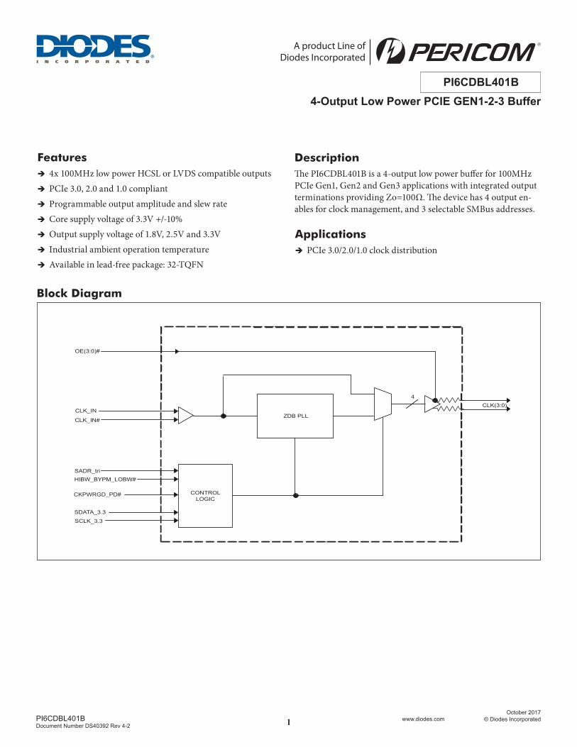
Block Diagram
DescriptionThe PI6CDBL401B is a 4-output low power buffer for 100MHz PCIe Gen1, Gen2 and Gen3 applications with integrated output terminations providing Zo=100Ω. The device has 4 output en-ables for clock management, and 3 selectable SMBus addresses.
Features ÎÎ 4x 100MHz low power HCSL or LVDS compatible outputsÎÎ PCIe 3.0, 2.0 and 1.0 compliantÎÎ Programmable output amplitude and slew rateÎÎ Core supply voltage of 3.3V +/-10%ÎÎ Output supply voltage of 1.8V, 2.5V and 3.3VÎÎ Industrial ambient operation temperatureÎÎ Available in lead-free package: 32-TQFN
CONTROLLOGIC
ZDB PLL
OE(3:0)#
CLK_IN
CLK_IN#
SADR_triHIBW_BYPM_LOBW#
CKPWRGD_PD#
SDATA_3.3
SCLK_3.3
CLK(3:0)4
ApplicationsÎÎ PCIe 3.0/2.0/1.0 clock distribution
4-Output Low Power PCIE GEN1-2-3 BufferPI6CDBL401B
A product Line ofDiodes Incorporated
222PI6CDBL401BDocument Number DS40392 Rev 4-2
www.diodes.com October 2017
© Diodes Incorporated
PI6CDBL401B
A product Line ofDiodes Incorporated
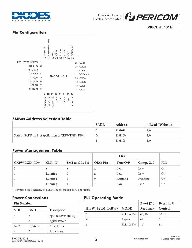
SMBus Address Selection TableSADR Address + Read / Write bit
State of SADR on first application of CKPWRGD_PD#0 1101011 1/0M 1101100 1/01 1101101 1/0
Power Management Table
CKPWRGD_PD# CLK_IN SMBus OEx bit OEx# Pin
CLKx
PLLTrue O/P Comp. O/P
0 x x x Low Low Off1 Running 0 x Low Low On1
1 Running 1 0 Running Running On1
1 Running x 1 Low Low On1
1. If bypass mode is selected, the PLL will be off, and outputs will be running
Power ConnectionsPin Number
DescriptionVDD GND
4 7 Input receiver analog9 8 Digital Power16, 25 15, 26, 30 DIF outputs21 20 PLL Analog
PLL Operating Mode
HiBW_BypM_LoBW# MODEByte1 [7:6]Readback
Byte1 [4:3]Control
0 PLL Lo BW 00, 10 00, 10M Bypass 01 011 PLL Hi BW 11 11
Pin Configuration
1
2
3
4
5
6
7
8
24
23
22
21
20
19
18
17
OE2#
CLK2#
CLK2
VDDA3.3
GNDA
CLK1#
CLK1
OE1#
HIBW_BYPM_LOBW#
FB_DNC
FB_DNC#
VDDR3.3
CLK_IN
CLK_IN#
GNDR
GNDDIG
9 10 11 12 13 14 15 16
32 31 30 29 28 27 26 25
VDD
DIG
3.3
SC
LK_3
.3
SDAT
A_3.
3
OE0
#
CLK
0
CLK
0#
GN
D
VDD
O1.
8
SAD
R_t
ri
CKP
WR
GD
_PD
#
GN
D
OE3
#
CLK
3#
CLK
3
GN
D
VDD
O1.
8
PI6CDBL401B
333PI6CDBL401BDocument Number DS40392 Rev 4-2
www.diodes.com October 2017
© Diodes Incorporated
PI6CDBL401B
A product Line ofDiodes Incorporated
Pin Descriptions Pin# Pin Name Type Description
1 HIBW_BYPM_LOBW# Input Trilevel input to select High BW, Bypass or Low BW mode. See PLL Operating
Mode Table for Details.
2 FB_DNC Output True clock of differential feedback. The feedback output and feedback input are connected internally on this pin. Do not connect anything to this pin.
3 FB_DNC# Output Complement clock of differential feedback. The feedback output and feedback input are connected internally on this pin. Do not connect anything to this pin.
4 VDDR3.3 Power 3.3V power for differential input clock (receiver). This VDD should be treated as an Analog power rail and filtered appropriately.
5 CLK_IN Input True Input for differential reference clock.6 CLK_IN# Input Complementary Input for differential reference clock.7 GNDR Power Analog Ground pin for the differential input (receiver)8 GNDDIG Power Ground pin for digital circuitry9 VDDDIG3.3 Power 3.3V digital power (dirty power)10 SCLK_3.3 Input Clock pin of SMBus circuitry, 3.3V tolerant.11 SDATA_3.3 Input/Output Data pin for SMBus circuitry, 3.3V tolerant.
12 OE0# Input Active low input for enabling DIF pair 0. This pin has an internal pull-down. 1 =disable outputs, 0 = enable outputs
13 CLK0 Output Differential true clock output14 CLK0# Output Differential Complementary clock output15 GND Power Ground pin.16 VDDO1.8 Power Power supply for outputs, range from 1.8V~3.3V.
17 OE1# Input Active low input for enabling DIF pair 1. This pin has an internal pull-down. 1 =disable outputs, 0 = enable outputs
18 CLK1 Output Differential true clock output19 CLK1# Output Differential Complementary clock output20 GNDA Power Ground pin for the PLL core.21 VDDA3.3 Power 3.3Vpower for the PLL core.22 CLK2 Output Differential true clock output23 CLK2# Output Differential Complementary clock output
24 OE2# Input Active low input for enabling DIF pair 2. This pin has an internal pull-down. 1 =disable outputs, 0 = enable outputs
25 VDDO1.8 Power Power supply for outputs, range from 1.8V~3.3V.26 GND Power Ground pin.27 CLK3 Output Differential true clock output28 CLK3# Output Differential Complementary clock output
29 OE3# Input Active low input for enabling DIF pair 3. This pin has an internal pull-down. 1 =disable outputs, 0 = enable outputs
30 GND Power Ground pin.

444PI6CDBL401BDocument Number DS40392 Rev 4-2
www.diodes.com October 2017
© Diodes Incorporated
PI6CDBL401B
A product Line ofDiodes Incorporated
Pin# Pin Name Type Description
31 CKPWRGD_PD# InputInput notifies device to sample latched inputs and start up on first high asser-tion. Low enters Power Down Mode, subsequent high assertions exit Power Down Mode. This pin has internal pull-up resistor.
32 SADR_tri Input Tri-level latch to select SMBus Address. See SMBus Address Selection Table.
Pin Descriptions Cont...
555PI6CDBL401BDocument Number DS40392 Rev 4-2
www.diodes.com October 2017
© Diodes Incorporated
PI6CDBL401B
A product Line ofDiodes Incorporated
Supply Voltage to Ground Potential ......................................................4.6VAll Inputs and Output ..................................................... -0.5V toVDD+0.5VAmbient Operating Temperature ........................................... -40 to +85°CStorage Temperature .......................................................... –65°C to +150°CJunction Temperature .......................................................................... 125°CSoldering Temperature .........................................................................260°CESD Protection (Input) ...........................................................2000V(HBM)
Note: Stresses greater than those listed under MAXIMUM RAT-INGS may cause permanent damage to the device. This is a stress rating only and functional operation of the device at these or any other conditions above those indicated in the operational sections of this specification is not implied. Exposure to absolute maximum rating conditions for extended periods may affect reliability.
Maximum Ratings(Above which useful life may be impaired. For user guidelines, not tested.)
Electrical Characteristics–Clock Input Parameters (TA = -40~85oC; VDD = 3.3V+/-10%; VDDO =
3.3V+/-10%; VDDO = 2.5V+/-10%; VDDO = 1.8V+/-10%, See Test Loads for Loading Conditions)
Symbol Parameters Condition Min. Type Max. Units
VIHDIF Input High Voltage - CLK_IN1Differential inputs(single-ended measurement)
600 800 1150 mV
VILDIF Input Low Voltage - CLK_IN1,3Differential inputs(single-ended measurement)
VSS - 300 0 300 mV
VCOM
Input Common Mode Voltage - CLK_IN1 Common Mode Input Voltage 300 725 mV
VSWING Input Amplitude - CLK_IN1 Peak to Peak value (VIHDIF - VILDIF) 300 1450 mVdv/dt Input Slew Rate - CLK_IN1,2 Measured differentially 0.4 V/nsIIN Input Leakage Current1 VIN = VDD , VIN = GND -5 5 uAdtin Input Duty Cycle1 Measurement from differential wavefrom 45 55 %JDIFIn Input Jitter - Cycle to Cycle1 Differential Measurement 0 150 ps
Note:1. Guaranteed by design and characterization, not 100% tested in production.2. Slew rate measured through +/-75mV window centered around differential zero3. The device can be driven from a single ended clock by driving the true clock and biasing the complement clock input to the VBIAS, where VBIAS is (VIH-
HIGH - VIHLOW)/2
Electrical Characteristics–Input/Supply/Common Parameters–Normal Operating
Conditions
(TA = -40~85oC; VDD = 3.3V+/-10%; VDDO = 3.3V+/-10%; VDDO = 2.5V+/-10%; VDDO = 1.8V+/-10%, See Test Loads for Loading Conditions)
Symbol Parameters Condition Min. Type Max. Units
VDDX Supply Voltage1 Supply voltage for core, analog 3.0 3.3 3.6 V
VDDO Supply Voltage1 Supply voltage outputs2.97 3.3 3.63
V2.25 2.5 2.751.62 1.8 1.98
TA
Ambient OperatingTemperature1
-40 25 85 °C

666PI6CDBL401BDocument Number DS40392 Rev 4-2
www.diodes.com October 2017
© Diodes Incorporated
PI6CDBL401B
A product Line ofDiodes Incorporated
Symbol Parameters Condition Min. Type Max. Units
VIH Input High Voltage1 Single-ended inputs, except SMBus, SADR_tri 0.65 VDD VDD +0.3 V
VIM Input Mid Voltage1 SADR_tri 0.4 VDD 0.6 VDD VVIL Input Low Voltage1 Single-ended inputs, except SMBus, SADR_tri -0.3 0.35 VDD VVH Hysteresis Voltage1 VT+ - VT- 0.05 VDD 0.2 VDD V
VOH Output High Voltage1 Single-ended outputs, except SMBus. IOH = -2mA
VDD -0.45 V
VOL Outputt Low Voltage1 Single-ended outputs, except SMBus. IOL = -2mA 0.45 V
IIN
Input Current1
Single-ended inputs, VIN = GND, VIN = VDD -5 5 uA
IINP
Single-ended inputsVIN = 0 V; Inputs with internal pull-up resistorsVIN = VDD; Inputs with internal pull-down resistors
-200 200 uA
fin Input Frequency1Bypass mode 1 400 MHz100MHz PLL mode 95 100 105 MHz
Lpin Pin Inductance1 7 nHCIN Capacitance1
Control Inputs 1.5 5 pFCout Output pin capacitance 6 pF
tSTAB
Clock output Stabiliza-tion1, 2
From VDD Power-Up and after input clockstabilization or de-assertion of CKPWRGD_PD# to 1st clock
0.6 1 ms
fMODIN
Input SS Modulation Frequency1
Allowable Frequency(Triangular Modulation)
30 31.500 33 kHz
tLATOE# OE# Latency1, 3CLK start after OE# assertionCLK stop after OE# deassertion
1 3 clocks
tDRVPD Tdrive_PD#1, 3CLK output enable afterCKPWRGD_PD# de-assertion
300 us
tF Fall time1, 2 Control inputs 5 nstR Rise time1, 2 Control inputs 5 ns
VILSMB
SMBus Input Low Volt-age1 0.8 V
VIHSMB
SMBus Input High Volt-age1 2.1 3.6 V
Electrical Characteristics–Input/Supply/Common Parameters–Normal Operating Conditions Cont...
777PI6CDBL401BDocument Number DS40392 Rev 4-2
www.diodes.com October 2017
© Diodes Incorporated
PI6CDBL401B
A product Line ofDiodes Incorporated
Electrical Characteristics–Input/Supply/Common Parameters–Normal Operating Conditions Cont...
Note:1. Guaranteed by design and characterization, not 100% tested in production.2. Control input must be monotonic from 20% to 80% of input swing. Input Frequency Capacitance3. Time from deassertion until outputs are >200 mV4. The differential input clock must be running for the SMBus to be active
Symbol Parameters Condition Min. Type Max. Units
VOLSMB SMBus Output Low Voltage1 @ IPULLUP 0.4 VIPULLUP SMBus Sink Current1 @ VOL 4 mAVDDSMB Nominal Bus Voltage1 3.3V bus voltage 2.7 3.6 VtRSMB SCLK/SDATA Rise Time1 (Max VIL - 0.15) to (Min VIH + 0.15) 1000 nstFSMB SCLK/SDATA Fall Time1 (Min VIH + 0.15) to (Max VIL - 0.15) 300 nsfMAXSMB SMBus Operating Frequency1, 5 Maximum SMBus operating frequency 400 kHz
Electrical Characteristics–CLK 0.7V Low Power HCSL Outputs (TA = -40~85oC; VDD = 3.3V+/-10%;
VDDO = 3.3V+/-10%; VDDO = 2.5V+/-10%; VDDO = 1.8V+/-10%, See Test Loads for Loading Conditions)
Symbol Parameters Condition Min. Type Max. Units
Trf Slew rate1,2,3
Scope averaging on 2.0V/ns setting @100MHz output 1 2 3 V/ns
Scope averaging on 3.0V/ns setting @100MHz output 2 3 4.5 V/ns
ΔTrf Slew rate matching1,2,4 Slew rate matching, Scope averaging on 7 20 %VHIGH Voltage High1,7 Statistical measurement on single-ended signal
using oscilloscope math function. (Scope averaging on)
660 880 mV
VLOW Voltage Low1,7 -150 150 mV
Vmax Max Voltage1 Measurement on single ended signal usingabsolute value. (Scope averaging off)
1150 mVVmin Min Voltage1 -300 mVVswing Vswing1,2,7 Scope averaging off 300 mVVcross_abs Crossing Voltage (abs)1,5,7 Scope averaging off 250 550 mVΔ-Vcross Crossing Voltage (var)1,6 Scope averaging off 140 mV
Note:1. Guaranteed by design and characterization, not 100% tested in production.2. Measured from differential waveform3. Slew rate is measured through the Vswing voltage range centered around differential 0V. This results in a +/-150mV window around differential 0V.4. Matching applies to rising edge rate for Clock and falling edge rate for Clock#. It is measured using a +/-75mV window centered on the average cross point
where Clock rising meets Clock# falling. The median cross point is used to calculate the voltage thresholds the oscilloscope is to use for the edge rate calcula-tions.
5. Vcross is defined as voltage where Clock = Clock# measured on a component test board and only applies to the differential rising edge (i.e. Clock rising and Clock# falling).
6. The total variation of all Vcross measurements in any particular system. Note that this is a subset of Vcross_min/max (Vcross absolute) allowed. The intent is to limit Vcross induced modulation by setting Δ-Vcross to be smaller than Vcross absolute.
7. At default SMBus settings.

888PI6CDBL401BDocument Number DS40392 Rev 4-2
www.diodes.com October 2017
© Diodes Incorporated
PI6CDBL401B
A product Line ofDiodes Incorporated
Electrical Characteristics–Output Duty Cycle, Jitter, Skew and PLL Characterisitics
(TA = -40~85oC; VDD = 3.3V+/-10%; VDDO = 3.3V+/-10%; VDDO = 2.5V+/-10%; VDDO = 1.8V+/-10%, See Test Loads
for Loading Conditions)
Symbol Parameters Condition Min. Type Max. Units
tDC Duty Cycle1 Measured differentially, PLL Mode 45 55 %tDCD Duty Cycle Distortion1,3 Measured differentially, Bypass Mode@100MHz -1 0 1 %tpdBYP Skew, Input to Output1,4
Bypass Mode, VT = 50% 2500 4500 pstpdPLL PLL Mode VT = 50% -250 250 pstskew Skew, Output to Output1,2 VT = 50% 25 50 ps
tjcyc-cyc Jitter, Cycle to cycle1,2
PLL mode @100MHz output 50 psAdditive Jitter in Bypass Mode @100MHz output 0.1 25 ps
Note:1. Guaranteed by design and characterization, not 100% tested in production.2. Measured from differential waveform3. Duty cycle distortion is the difference in duty cycle between the output and the input clock when the device is operated in bypass mode.4. All outputs at default slew rate5. The MIN/TYP/MAX values of each BW setting track each other, i.e., Low BW MAX will never occur with Hi BW MIN.
Electrical Characteristics–Current Consumption (TA = -40~85oC; See Test Loads for Loading Conditions)
Symbol Parameters Condition Min. Type Max. Units
IDDAOP
Operating Supply Current1
VDDA+VDDR, PLL Mode, @100MHz, typical value under VDDO = 1.8V 37 45 mA
IDDOP
VDD1.8, All outputs active @100MHz, typical value under VDDO = 1.8V 52 60 mA
IDDAPD Powerdown Current1,2VDDA+VDDR, PLL Mode, @100MHz 1 mA
IDDPD VDD1.8, Outputs Low 1.8 mA
Note:1. Guaranteed by design and characterization, not 100% tested in production.2. Input clock stopped.
999PI6CDBL401BDocument Number DS40392 Rev 4-2
www.diodes.com October 2017
© Diodes Incorporated
PI6CDBL401B
A product Line ofDiodes Incorporated
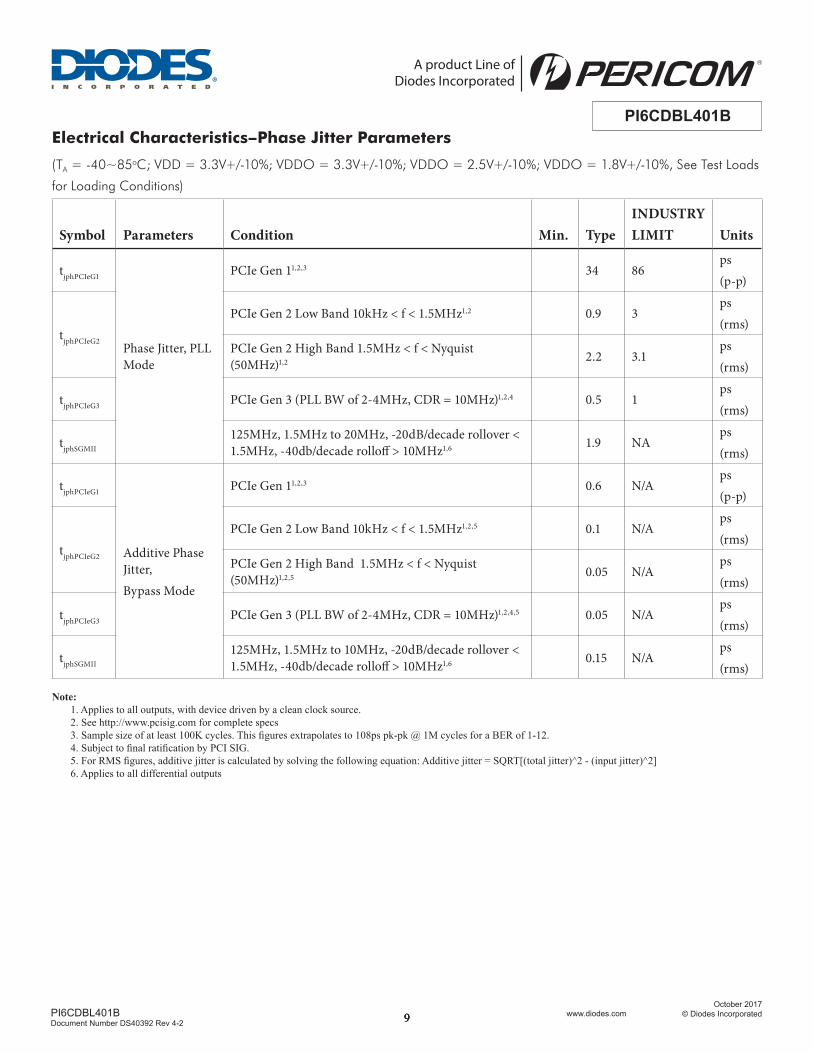
Electrical Characteristics–Phase Jitter Parameters
(TA = -40~85oC; VDD = 3.3V+/-10%; VDDO = 3.3V+/-10%; VDDO = 2.5V+/-10%; VDDO = 1.8V+/-10%, See Test Loads
for Loading Conditions)
Symbol Parameters Condition Min. TypeINDUSTRYLIMIT Units
tjphPCIeG1
Phase Jitter, PLL Mode
PCIe Gen 11,2,3 34 86ps(p-p)
tjphPCIeG2
PCIe Gen 2 Low Band 10kHz < f < 1.5MHz1,2 0.9 3ps(rms)
PCIe Gen 2 High Band 1.5MHz < f < Nyquist (50MHz)1,2 2.2 3.1
ps(rms)
tjphPCIeG3 PCIe Gen 3 (PLL BW of 2-4MHz, CDR = 10MHz)1,2,4 0.5 1ps(rms)
tjphSGMII
125MHz, 1.5MHz to 20MHz, -20dB/decade rollover < 1.5MHz, -40db/decade rolloff > 10MHz1,6 1.9 NA
ps(rms)
tjphPCIeG1
Additive Phase Jitter,Bypass Mode
PCIe Gen 11,2,3 0.6 N/Aps (p-p)
tjphPCIeG2
PCIe Gen 2 Low Band 10kHz < f < 1.5MHz1,2,5 0.1 N/Aps(rms)
PCIe Gen 2 High Band 1.5MHz < f < Nyquist (50MHz)1,2,5 0.05 N/A
ps(rms)
tjphPCIeG3 PCIe Gen 3 (PLL BW of 2-4MHz, CDR = 10MHz)1,2,4,5 0.05 N/Aps(rms)
tjphSGMII
125MHz, 1.5MHz to 10MHz, -20dB/decade rollover < 1.5MHz, -40db/decade rolloff > 10MHz1,6 0.15 N/A
ps(rms)
Note:1. Applies to all outputs, with device driven by a clean clock source.2. See http://www.pcisig.com for complete specs3. Sample size of at least 100K cycles. This figures extrapolates to 108ps pk-pk @ 1M cycles for a BER of 1-12.4. Subject to final ratification by PCI SIG.5. For RMS figures, additive jitter is calculated by solving the following equation: Additive jitter = SQRT[(total jitter)^2 - (input jitter)^2]6. Applies to all differential outputs
101010PI6CDBL401BDocument Number DS40392 Rev 4-2
www.diodes.com October 2017
© Diodes Incorporated
PI6CDBL401B
A product Line ofDiodes Incorporated
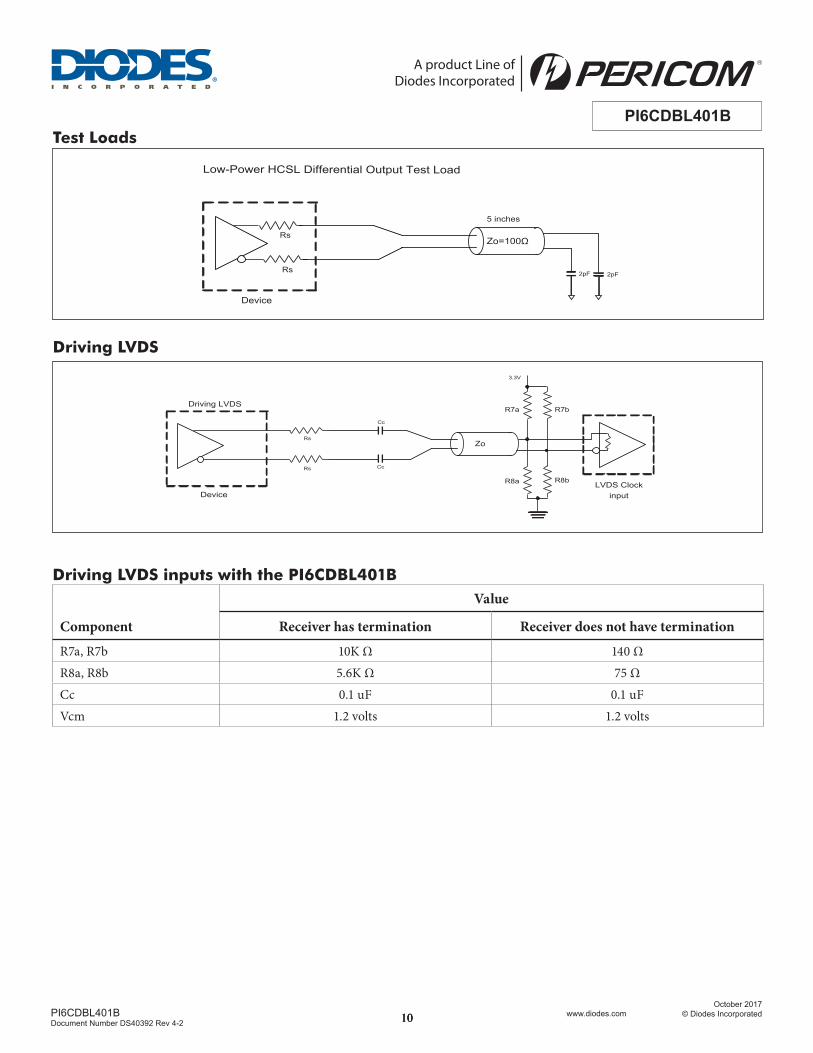
Driving LVDS inputs with the PI6CDBL401B
Component
Value
Receiver has termination Receiver does not have termination
R7a, R7b 10K Ω 140 ΩR8a, R8b 5.6K Ω 75 ΩCc 0.1 uF 0.1 uFVcm 1.2 volts 1.2 volts
Test Loads
Rs
RO
5 inches
Rs
Zo=100Ω
2pF 2pF
Low-Power HCSL Differential Output Test Load
Device
Driving LVDS
R
Zo
Device
Driving LVDS
Cc
Cc
R7a R7b
R8a R8b
3.3V
LVDS Clockinput
Rs
Rs

111111PI6CDBL401BDocument Number DS40392 Rev 4-2
www.diodes.com October 2017
© Diodes Incorporated
PI6CDBL401B
A product Line ofDiodes Incorporated
Serial Data Interface (SMBus)This part is a slave only device that supports blocks read and block write protocol using a single 7-bit address and read/write bit as shown below.Read and write block transfers can be stopped after any complete byte transfer by issuing STOP.
Address AssignmentRefer to SMBus Address Selection Table.
Data Protocol(Write)
1 bit 8 bits 1 8 bits 1 8 bits 1 8 bits 1 8 bits 1 1 bit
Start bit Slave Addr: D4 Ack Register
offset Ack Byte Count=N Ack Data
Byte 0 Ack … Data Byte N-1 Ack Stop bit
(Read)
1 bit 8 bits 1 8 bits 1 1 8 bits 1 8 bits 1 8 bits 1 8 bits 1 1 bit
Start bit Slave Addr: D4 Ack Register
offset Ack Repeat start
Slave Addr: D5 Ack Byte
Count=N Ack Data Byte 0 Ack … Data Byte
N-1NOT Ack
Stop bit
Note:
1. Register offset for indicating the starting register for indexed block write and indexed block read. Byte Count in write mode cannot be 0.
121212PI6CDBL401BDocument Number DS40392 Rev 4-2
www.diodes.com October 2017
© Diodes Incorporated
PI6CDBL401B
A product Line ofDiodes Incorporated
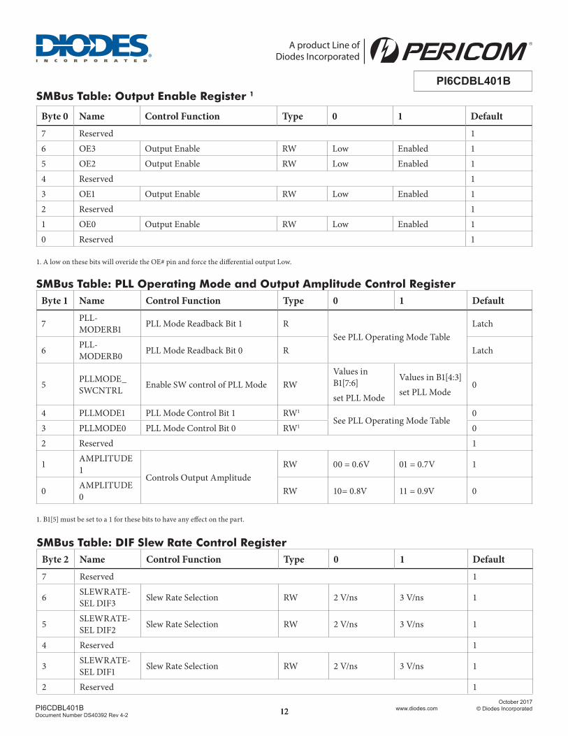
SMBus Table: Output Enable Register 1
Byte 0 Name Control Function Type 0 1 Default
7 Reserved 16 OE3 Output Enable RW Low Enabled 15 OE2 Output Enable RW Low Enabled 14 Reserved 13 OE1 Output Enable RW Low Enabled 12 Reserved 11 OE0 Output Enable RW Low Enabled 10 Reserved 1
1. A low on these bits will overide the OE# pin and force the differential output Low.
SMBus Table: DIF Slew Rate Control RegisterByte 2 Name Control Function Type 0 1 Default
7 Reserved 1
6 SLEWRATE-SEL DIF3 Slew Rate Selection RW 2 V/ns 3 V/ns 1
5 SLEWRATE-SEL DIF2 Slew Rate Selection RW 2 V/ns 3 V/ns 1
4 Reserved 1
3 SLEWRATE-SEL DIF1 Slew Rate Selection RW 2 V/ns 3 V/ns 1
2 Reserved 1
SMBus Table: PLL Operating Mode and Output Amplitude Control RegisterByte 1 Name Control Function Type 0 1 Default
7 PLL-MODERB1 PLL Mode Readback Bit 1 R
See PLL Operating Mode TableLatch
6 PLL-MODERB0 PLL Mode Readback Bit 0 R Latch
5 PLLMODE_SWCNTRL Enable SW control of PLL Mode RW
Values in B1[7:6]set PLL Mode
Values in B1[4:3]set PLL Mode
0
4 PLLMODE1 PLL Mode Control Bit 1 RW1
See PLL Operating Mode Table0
3 PLLMODE0 PLL Mode Control Bit 0 RW1 02 Reserved 1
1 AMPLITUDE 1
Controls Output AmplitudeRW 00 = 0.6V 01 = 0.7V 1
0 AMPLITUDE 0 RW 10= 0.8V 11 = 0.9V 0
1. B1[5] must be set to a 1 for these bits to have any effect on the part.
131313PI6CDBL401BDocument Number DS40392 Rev 4-2
www.diodes.com October 2017
© Diodes Incorporated
PI6CDBL401B
A product Line ofDiodes Incorporated
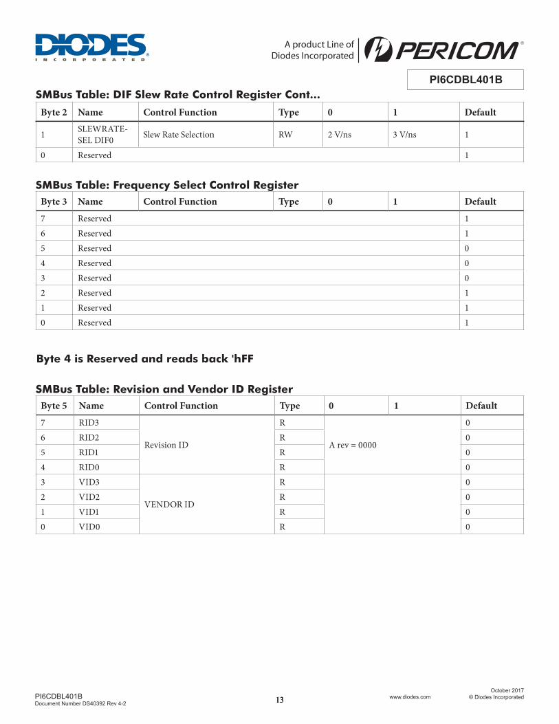
SMBus Table: Frequency Select Control RegisterByte 3 Name Control Function Type 0 1 Default
7 Reserved 16 Reserved 15 Reserved 04 Reserved 03 Reserved 02 Reserved 11 Reserved 10 Reserved 1
SMBus Table: Revision and Vendor ID RegisterByte 5 Name Control Function Type 0 1 Default
7 RID3
Revision ID
R
A rev = 0000
06 RID2 R 05 RID1 R 04 RID0 R 03 VID3
VENDOR ID
R 02 VID2 R 01 VID1 R 00 VID0 R 0
1 SLEWRATE-SEL DIF0 Slew Rate Selection RW 2 V/ns 3 V/ns 1
0 Reserved 1
SMBus Table: DIF Slew Rate Control Register Cont...
Byte 2 Name Control Function Type 0 1 Default
Byte 4 is Reserved and reads back 'hFF
141414PI6CDBL401BDocument Number DS40392 Rev 4-2
www.diodes.com October 2017
© Diodes Incorporated
PI6CDBL401B
A product Line ofDiodes Incorporated
SMBus Table: Device Type/Device IDByte 6 Name Control Function Type 0 1 Default
7 Device Type1Device Type
R 00 = FGV, 01 = DBV,10 = DMV, 11= Reserved
06 Device Type0 R 15 Device ID5
Device ID
R
000100 binary or 04 hex
04 Device ID4 R 03 Device ID3 R 02 Device ID2 R 11 Device ID1 R 00 Device ID0 R 0
SMBus Table: Byte Count RegisterByte 7 Name Control Function Type 0 1 Default
7 Reserved 06 Reserved 05 Reserved 04 Reserved 03 Reserved 02 Reserved 01 Reserved 00 Reserved 0
151515PI6CDBL401BDocument Number DS40392 Rev 4-2
www.diodes.com October 2017
© Diodes Incorporated
PI6CDBL401B
A product Line ofDiodes Incorporated
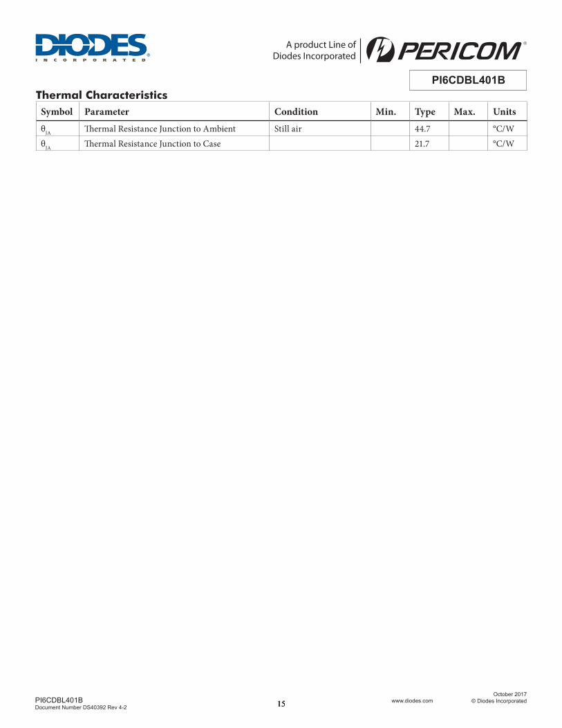
Thermal CharacteristicsSymbol Parameter Condition Min. Type Max. Units
θJA Thermal Resistance Junction to Ambient Still air 44.7 °C/WθJA Thermal Resistance Junction to Case 21.7 °C/W
161616PI6CDBL401BDocument Number DS40392 Rev 4-2
www.diodes.com October 2017
© Diodes Incorporated
PI6CDBL401B
A product Line ofDiodes Incorporated
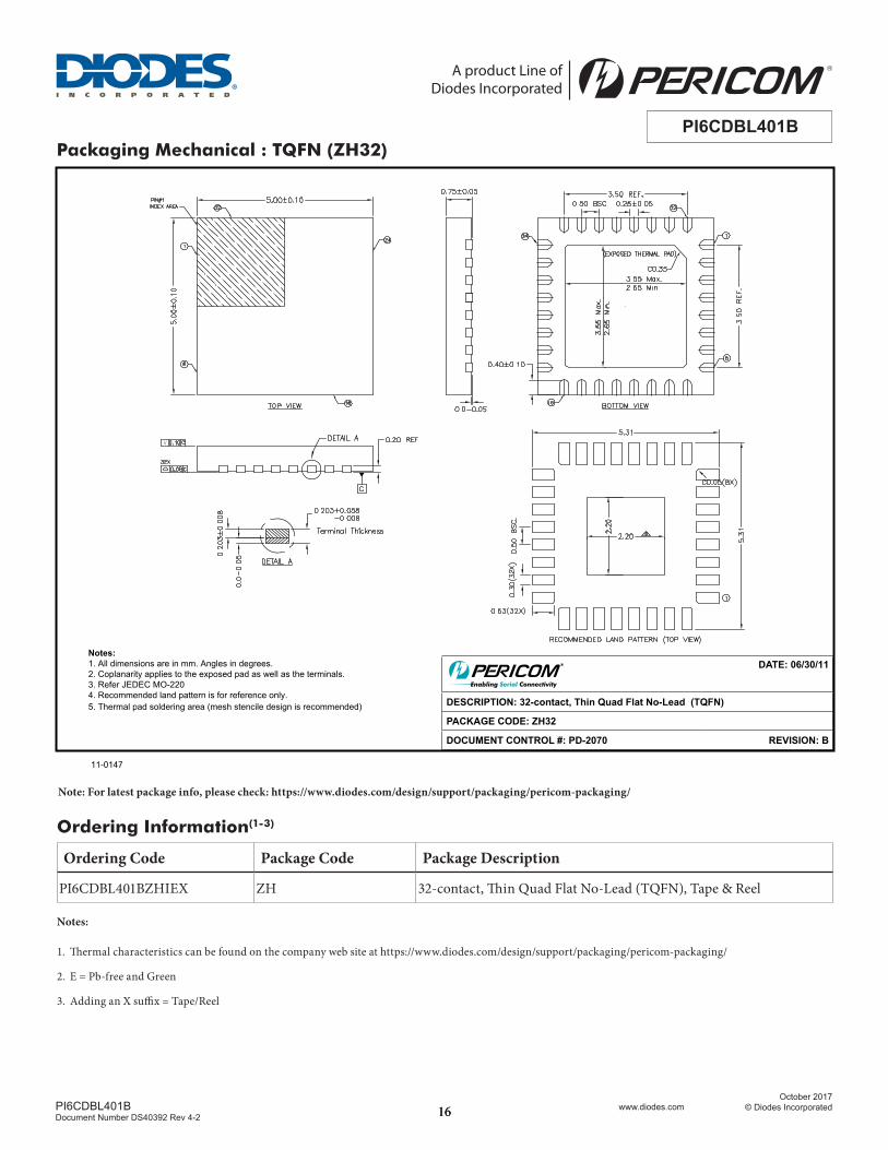
Packaging Mechanical : TQFN (ZH32)
DATE: 06/30/11
DESCRIPTION: 32-contact, Thin Quad Flat No-Lead (TQFN)
PACKAGE CODE: ZH32
DOCUMENT CONTROL #: PD-2070 REVISION: B
Notes:1. All dimensions are in mm. Angles in degrees.2. Coplanarity applies to the exposed pad as well as the terminals.3. Refer JEDEC MO-2204. Recommended land pattern is for reference only.5. Thermal pad soldering area (mesh stencile design is recommended)
11-0147
Ordering Information(1-3)
Ordering Code Package Code Package Description
PI6CDBL401BZHIEX ZH 32-contact, Thin Quad Flat No-Lead (TQFN), Tape & Reel
Notes:
1. Thermal characteristics can be found on the company web site at https://www.diodes.com/design/support/packaging/pericom-packaging/
2. E = Pb-free and Green
3. Adding an X suffix = Tape/Reel
Note: For latest package info, please check: https://www.diodes.com/design/support/packaging/pericom-packaging/

171717PI6CDBL401BDocument Number DS40392 Rev 4-2
www.diodes.com October 2017
© Diodes Incorporated
PI6CDBL401B
A product Line ofDiodes Incorporated
IMPORTANT NOTICE
DIODES INCORPORATED MAKES NO WARRANTY OF ANY KIND, EXPRESS OR IMPLIED, WITH REGARDS TO THIS DOCUMENT, INCLUDING, BUT NOT LIMITED TO, THE IMPLIED WARRANTIES OF MERCHANTABILITY AND FITNESS FOR A PARTICULAR PURPOSE (AND THEIR EQUIVALENTS UNDER THE LAWS OF ANY JURISDICTION).
Diodes Incorporated and its subsidiaries reserve the right to make modifications, enhancements, improvements, corrections or other changes without further no-tice to this document and any product described herein. Diodes Incorporated does not assume any liability arising out of the application or use of this document or any product described herein; neither does Diodes Incorporated convey any license under its patent or trademark rights, nor the rights of others. Any Customer or user of this document or products described herein in such applications shall assume all risks of such use and will agree to hold Diodes Incorporated and all the companies whose products are represented on Diodes Incorporated website, harmless against all damages.
Diodes Incorporated does not warrant or accept any liability whatsoever in respect of any products purchased through unauthorized sales channel.
Should Customers purchase or use Diodes Incorporated products for any unintended or unauthorized application, Customers shall indemnify and hold Diodes Incorporated and its representatives harmless against all claims, damages, expenses, and attorney fees arising out of, directly or indirectly, any claim of personal injury or death associated with such unintended or unauthorized application.
Products described herein may be covered by one or more United States, international or foreign patents pending. Product names and markings noted herein may also be covered by one or more United States, international or foreign trademarks.
This document is written in English but may be translated into multiple languages for reference. Only the English version of this document is the final and determi-native format released by Diodes Incorporated.
LIFE SUPPORT
Diodes Incorporated products are specifically not authorized for use as critical components in life support devices or systems without the express written approval of the Chief Executive Officer of Diodes Incorporated. As used herein:
A. Life support devices or systems are devices or systems which:
1. are intended to implant into the body, or
2. support or sustain life and whose failure to perform when properly used in accordance with instructions for use provided in the labeling can be reasonably expected to result in significant injury to the user.
B. A critical component is any component in a life support device or system whose failure to perform can be reasonably expected to cause the
failure of the life support device or to affect its safety or effectiveness.
Customers represent that they have all necessary expertise in the safety and regulatory ramifications of their life support devices or systems, and acknowledge and agree that they are solely responsible for all legal, regulatory and safety-related requirements concerning their products and any use of Diodes Incorporated products in such safety-critical, life support devices or systems, notwithstanding any devices- or systems-related information or support that may be provided by Diodes Incorporated. Further, Customers must fully indemnify Diodes Incorporated and its representatives against any damages arising out of the use of Diodes Incorporated products in such safety-critical, life support devices or systems.
Copyright © 2016, Diodes Incorporated
www.diodes.com