Embed Size (px)
Citation preview
0
A physical model for playing the ages old Indian game CHIDIYA UDD
EC-316 MICROPROCESSORS LAB ELECTRONICS AND COMMUNICATION DEPARTMENT
NETAJI SUBHAS INSTITUTE OF TECHNOLOGY DELHI UNIVERSITY
MAHIMA SINGH 93/ec/13 &
MANISHA GAHLOT 97/EC/13 3 JUNE 2016

1 | P a g e
ACKNOWLEDGEMENT With profound respect and gratitude we take the opportunity to
convey our sincere thanks to Prof. D.V. Gadre for introducing us to
such practicality of the subject and providing valuable guidance and
resourses leading to the accomplishment of the project titled as “8085
CHIDIYA UDD” based on 8085 Microproccessor.
Special thanks to our seniors and peers in CEDT for their constant
support and guidance.We would also like to thank the various lab
assisstants who patiently helped us during the course of the project
work.
We would also like to thank www.pcbpower.com for precise
manufacture and timely delievery of the project board.

2 | P a g e
TABLE OF CONTENTS
1. INTRODUCTION
2. ACKNOWLEDGEMENT
3. JUSTIFICATION & MOTIVATION
4. MATERIALS REQUIRED
5. PROJECT DESCRIPTION
6. A LOOK INTO THE SCHEMATIC
7. A LOOK INTO THE BOARD LAYOUT
8. MAIN BLOCK DIAGRAM
9. THE 8085
10. THE 8255
11. THE 8085
12. RAM AND ROM
13. DECODING CIRCUIT
14. THE CODE
15. TESTING THE BOARD
16. PROBLEMS FACED
17. GANTT CHART REVISITED
18. CONCLUSION
19. BIBLIOGRAPHY

3 | P a g e
INTRODUCTION 8085 CHIDIA UDD is a physical structure to play the ages old chidiya
udd game using 8085 which otherwise has no physical structure
available for it.The game basically consists of a LCD onto which the
names of objects would be displayed randomly and 2 switches
corresponding to 2 players who after seeing the displayed objects
name would make a quick decision whether the object flies or not .if
the object flies players release the switches and keep them pressed if it
doesn’t fly.the system would analayze the right and wrong moves and
accordingly display the score.The player with more score would be the
winner in the end.
MOTIVATION AND JUSTIFICATION As already known, ‘Chidiya Udd’ has been one of the most famous
games amongst kids. However there is currently no physical structure
available in the market which makes it possible to play this game. We
aim to create such a structure using the 8085 microprocessor. It shall
cater to entertainment and recreational needs as well as provides a
perfect example of simulating Indian traditions using technology.This is
what motivated dus to go about making this 8085 based challenging
project.

4 | P a g e
MATERIAL REQUIRED
S NO.
NAME OF COMPONENT
1. RESISTORS
2. CAPACITORS
3. 8085
4. 8255
5. LATCHES- 74573N
6. DECODER-74138N
7. PUSH BUTTONS
8. 32K EEPROM
9. 32K RAM
10. RED LEDS
11. 16 * 2 LIQUID CRYSTAL DISPLAY
12. EEPROM PROGRAMMER
13. 10K POT
14. NOR GATE 7402
15. BERG STRIP
16. LC CRYSTAL 6MHZ
17. POWER CONNECTOR

5 | P a g e
A LOOK INTO THE SCHEMATIC

A LOOK INTO THE BOARD LAYOUT
This was the board obtained after making the schematic. The
board was routed after this keeping in view all the standard
measurement and sizes. The gebers were sent to pcb power
for final manufacture of our chidiya udd board

1 | P a g e
The project heart lies in the microprocessor 8085 which controls the logic , the peripherals and the memory. As the project doesn’t involve any interrupt logic the interrupt pins have been pulled down . A switch is connected to the SID pin which was used to test the microprocessor using SID SOD test. The address lines latched are connected to various points such as chip select of RAM, ROM, and 8255. A 32K RAM and 32K ROM has been used for the memory. 8255 has been used to interface the input switches on PORT A and LCD data lines on PORT B. 8255 is therefore used in MODE 0 I/O. PORT C lower pins are used for control pins of LCD.A micro USB connector has been used to power the board. A crystal of 6MHZ has been used as a clock. On powering the board the LCD shows chidiya udd.The game can be
played at a time by 2 players. The project comprises of a LCD screen
and 2 push buttons. One push button would be made available to 1
player.The LCD screens would show the name of the creature/object
under test and would simultaneously display the score.So now in the
beginning CHIDIYA UDD would be displayed on the screen, thereafter
we begin with our game .pressing of the push button indicates a not
flying action whereas release of the push button indicates a flying
action. So what basically needs to be done by the player is that when
a player sees the name of the creature/object on the screen , he
decides whether that object flies or not . if according to him it flies
he releases the button nd if it doesn’t fly he keeps the button
pressed. Now this display of names occurs randomly and every name
is displayed after 2 seconds. So the player effectively gets 2 sec to
judge that he should fly or not. The input given by the player on the
push buttons is analysed by the microprocessor and accordingly his

2 | P a g e
score is incremented by one if he makes a correct move . The person with the higher cumulative score in the end would win. A block diagram has been included for further reference.

3 | P a g e
BASIC BLOCK DIAGRAM
.
MIC
RO
PR
OC
ESSO
R
MEMORY
INP
UT
FRO
M P
USH
BU
TTO
NS
OU
TPU
T TO
LC
D D
ISP
LAY

THE 8085
8085 is an 8 bit microprocessor introduced by intel in 1976. This 40
pin IC is an update over the microprocessor 8080 and requires less
support circuitry, allowing simpler and less expensive microcomputer
systems to be built. It uses a multiplexed addess/data bus which
reduced the number of PCB tracks to memory segments.
While it has the conventional von Neumann design based . on 8080,
it still extends to incorporate 3 maskable vectored interrupts (RST 7.5
, 6.5 , 5.5) , a non vectored interrupt INTR. All the interrupts are
enabled using the instruction EI and disabled using DI. INTA is used
to send an acknowledgement to the device which requested an
interrupt.
It can accommodate slower peripherals using the READY pin
through externally generated wait states. It can drive itself using
the crystal

1 | P a g e
externally connected to X1 and X2, while a internal clock generation
uses a divide by two circuitry.
Although it does not require demultiplexing of address line to
generate the lower byte of the address, which can be done using a
latch whose enable pin is connected to ALE pin of the 8085. ALE pin
goes high at the start of every machine cycle, which enables the
addresss latch.
Read control signal which is active low indicates that the selected I/O
or memory device is to be read and data are available on the data
bus. Write control signal which is active low indicates that the data
on the data bus are to be written into a selected memory or i/o port.
IO/M* is a status signal used to differenciate between I/O and
memory operations. When it is low it indicates a memory operation
and when high it indicates a I/O operation. The signal is combined
with RD* and WR* to generate input output and memory signals. S1
& S0 are status signals.
HLDA signal acknowledges a hold request. HOLD signal indicates that
a external peripheral such as a DMA controller is requesting the use
of address and data bus.READY is used to delay the microprocessor
read or write cycles to synchronise a slow peripheral with the 8085.
RESET IN * when the signal on this pin goes low, the program
counter is set to zero and the buses are tristated and the MPU is
reset. RESET OUT signal indicates that the MPU is being reset. The
signal can be used to reset other devices.

PCB LAYOUT
1 | P a g e
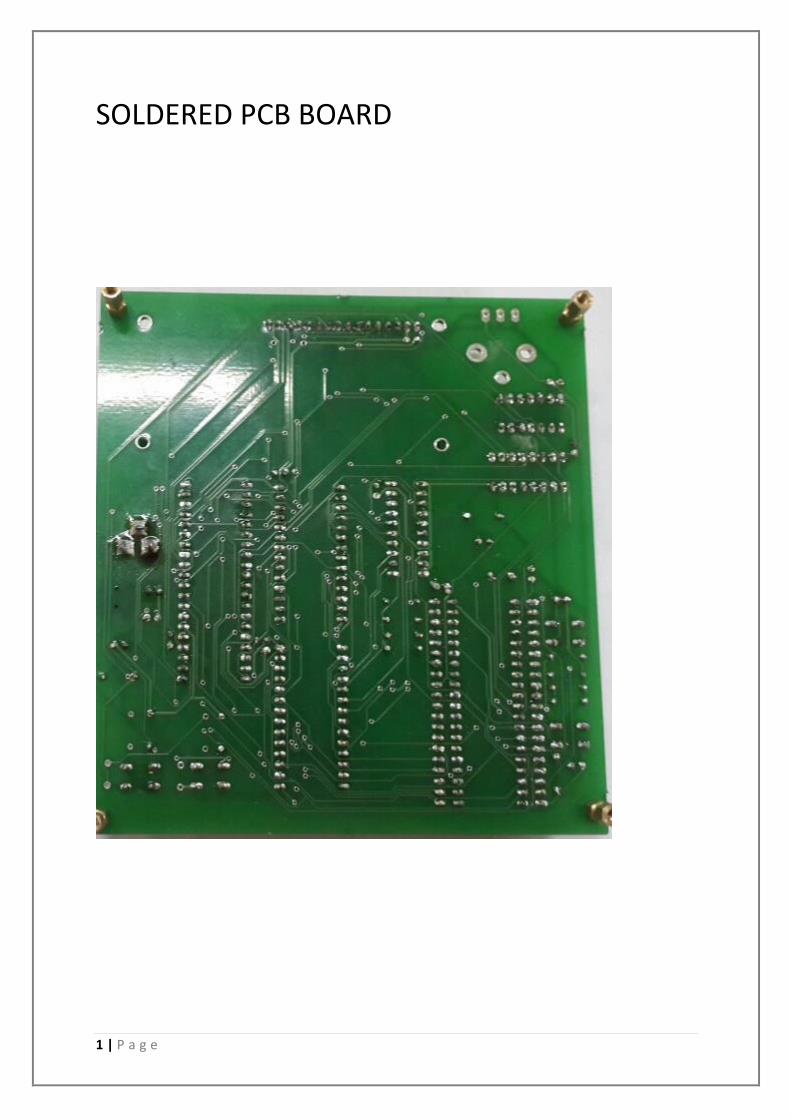
SOLDERED PCB BOARD

2 | P a g e
SOLDERED BOARD

3 | P a g e
FINAL WORKING BOARD

THE 8255 The 8255 has 24 input/output pins in all.[5] These are divided into three 8-bit ports (Port A, Port B, Port C).[6] Port A and port B can be used as 8-bit input/output ports. Port C can be used as an 8-bit input/output port or as two 4-bit input/output ports or to produce handshake signals for ports A and B.
The three ports are further grouped as follows:
1. Group A consisting of port A and upper part of port C.
2. Group B consisting of port B and lower part of port C.
Eight data lines (D0 - D7) are available (with an 8-bit data buffer) to read/write data into the ports or control register under the status of the RD (pin 5) and WR (pin 36), which are active low signals for read and write operations respectively. The address lines A1 and A0allow to successively access any one of the ports or the control register as listed below:
A1 A0 Port selected
0 0 port A
0 1 port B
1 0 port C
1 1 control register
The control signal chip select CS (pin 6) is used to enable the 8255 chip. It is an active low signal, i.e., when CS = '0', the 8255 is enabled. The RESET input (pin 35) is connected to the RESET line of system like

1 | P a g e
8085, 8086, etc., so that when the system is reset, all the ports are initialized as input lines. This is done to prevent 8255 and/or any peripheral connected to it, from being destroyed due to mismatch of ports. As an example, consider an input device connected to 8255 at port A. If from the previous operation, port A is initialized as an output port and if 8255 is not reset before using the current configuration, then there is a possibility of damage of either the input device connected or 8255 or both since both 8255 and the device connected will be sending out data.
The control register or the control logic or the command word register is an 8-bit register used to select the modes of operation and input/output designation of the ports.
We use 8255 in mode 0.
Mode 0 - simple I/O
In this mode, the ports can be used for simple I/O operations without handshaking signals. Port A, port B provide simple I/O operation. The two halves of port C can be either used together as an additional 8-bit port, or they can be used as individual 4-bit ports. Since the two halves of port C are independent, they may be used such that one-half is initialized as an input port while the other half is initialized as an output port.
The input/output features in mode 0 are as follows:
1. Output ports are latched.
2. Input ports are buffered, not latched.
3. Ports do not have handshake or interrupt capability.
4. With 4 ports, 16 different combinations of I/O are possible.
THE RAM AND ROM
RAM or Random Access Memory is used basically to store data
while running the program. We can both read and write data into
it. This memory is volatile. When the power is turned off, all its
contents are destroyed.
ROM or Read Only Memory is the main memory of the brain
8085. 8085 fetches instructions saved sequentially in the ROM.
Saved on the ROM is the entire program that the 8085 has to
execute. We can only read from the ROM once it is connected to
the board.We have used EEPROM which is Electrically Erasable
Programmable Read Only Memory, since the information stored
in this memory can be altered using electrical signals. Unlike RAM
its contents do not get destroyed when power is turned off and to
write data into it we need an EEPROM programmer.
RAM and ROM come in various sizes. We have chosen 32K ROM
and 32K RAM. Our work could have been easily accomplished by
8K ROM and 8K RAM but to be on the safe side we took a larger
memory. A larger memory leads to slight variations only in the
interfacing circuitry rest of the connections remain the same.

THE DECODING CIRCUIT
The decoding circuit is basically used to enable the RAM,ROMand
the I/O devices at the right time.
A decoder identifies each combination at its input and decoded it
into its binary equivalent. It commonly used in interfacing I/O
peripherals and memory. Decoders are also in built in memory
chip to select specific registers in it.
In our project we have used 3x8 decoder(in-order to
accommodate any future change as wells).
Address lines A15, A14 and,A13 have been used as input to
decoder 74138
A1
5
A1
4
A1
3
LOGIC
0 0 0 ROM ENABLE
0 1 0 RAM ENABLE
1 0 0 LED ROW ENABLE
1 0 1 LED COLUMN ENABLE
The decoder circuit can be replaced by use of logic gates.
THE CODE
.ORG 0000H
LXI SP,0000H ;STACK POINTER INITIALISATION
MVI A, 00H
LXI H, 8000H
MOV M, A ;initial score for P1
INX H
MOV M, A ;initial score for P2
MVI A,090H ;8255 INITIALISATION
OUT 003H
INIT: MVI A,030H
MOV B,A
CALL OUTPUT
CALL CMDOUT
CALL CMDOUT
MVI A,038H ;8 BIT, 2 LINES, 5X8 DISP
CALL CMDOUT
MVI A,008H ;DISPLAY OFF
CALL CMDOUT
MVI A,001H ;CLEAR DISPLAY
CALL CMDOUT
MVI A,006H ;ENTRY MODE SET, SHIFT AND INCREMENT
CURSOR
CALL CMDOUT
MVI A,00CH ;DISPLAY ON CURSOR, BLINKING OFF
CALL CMDOUT
DISPW1: MVI A, 01H; CLEARING DISPLAY
CALL CMDOUT
MVI A, 84H

1 | P a g e
CALL CMDOUT
LXI H, WD1 ; POINTER TO WD1 STRING
A1: MOV A, M
CPI 00H
JZ DISP1 ;ZERO MEANS WE HAVE REACHED END OF
WORD
CALL DTAOUT
INX H ;GO TO THE NEXT BIT IN THE WORD
JMP A1
LXI H, Birds; POINTER TO birdstart BIRDSTART WILL BE
THE LABEL FOR STORING THE STACK OF BIRDS. USE FORMAT AS
GIVYEN. NEED NOT DEFINE MEMORY LOCATIONS.
DISP1: CALL DELAY
A2: MVI A,001H
CALL CMDOUT
MVI A, 0C3H
CALL CMDOUT
A3: MOV A, M
CPI 00H
JZ notfly
CPI 01H
JZ fly
CALL DTAOUT
INX H
JMP A3 ;display bird name
notfly: MVI B, 00H
INX H
JMP POLL
fly: MVI B, 01H
2 | P a g e
INX H
JMP POLL
POLL: MVI A, 10010000B ;8255 INITIALISATION ;IT IS
KEEPING TRACK OF RECEIVING INPUTS AND WORKING ON C. AS
LONG AS C IS LESS THAN
OUT 03H
MVI C, 03H
L1: MVI D, 0FFH
MVI E, 0FFH
READ1: IN 00H
ANI 03H
CPI 02H; ; comparision being made for the
switch of player 1
JZ CALC2
CPI 01H; ;player2 PRESSED
JZ CALC1
DCX D
MOV A,E
ORA D
JNZ READ1
DCR C
MOV A, C
CPI 00H
JNZ L1
JZ CALC3
CALC2: PUSH H
LXI H, 8000H
MOV D, M
INX H

3 | P a g e
MOV E, M ; get scores in D, E
registers
MOV A, B; get value for bird ; PROCESSING OF
INPUT GIVEN BY PLAYER1
CPI 01H
JNZ NEGP1
INR D
LXI H, 8000H
MOV M, D
CALL DISPS
POP H
JMP DISP1; go to display for next animal
NEGP1: MOV A, D
CPI 00H
JZ NOP1
DCR D
LXI H, 8000H
MOV M, D
NOP1: CALL DISPS
POP H
JMP DISP1;
CALC1: PUSH H ; WHEN P2 HAS PRESSED
LXI H, 8000H ; RETRIEVES ORIGINAL SCORES OF P1 AND P2
MOV D, M
INX H
MOV E, M ; get scores in D, E
registers
MOV A, B; get value for bird PROCESSING IF
INPUT COMES FROM PLAYER1. WE CHECK IF INPUT IS
RIGHT/WRONG IN ACCORDANCE WITH THE CURRENT BIRD AND
HENCE INCREMENT/DECREMENT THE SCORE

4 | P a g e
CPI 01H ;BITS FROM ORIGINAL BIRD WORD THAT WERE
STORED IN B ARE NOW BEING COMPARED WITH 01 WHICH IS
FLYING KE LIYE
JNZ NEGP2 ; BIRD IS NOT FLYING. BUT P2 HAS SAID THAT
THE BIRD FLIES
INR E ; SCORE OF P2
LXI H, 8001H
MOV M, E
CALL DISPS
POP H
JMP DISP1 ;go to display for next animal:: THIS
WAS ERROR PREVIOUSLYYYYYYYYYYYYYYYYYYYYYY . EARLIER
WAS A1
NEGP2: MOV A, E
CPI 00H
JZ NOP2
DCR E
LXI H, 8001H
MOV M, E
NOP2: CALL DISPS
POP H
JMP DISP1;
CALC3: PUSH H
LXI H, 8000H
MOV D, M
INX H
MOV E, M ; get scores in D, E
registers
MOV A, B ;PROCESSING OF FINAL SCORES INCASE
NO PLAYER GIVES AN INPUT

5 | P a g e
CPI 00H ;B IS THE REGISTER THAT IS STORING
VALUES OO/O1. B=00 MEANS BIRD CANT FLY. ALSO NO SWITCH
BEING PRESSED MEANS SAME, THAT'S WHY WE ARE HERE IN
THIS LOOP. HENCE BOTH ARE CORRECT.
;NOW MOVE TO LABEL OF BOTH CORRECT WHERE BOTH WILL
BE REWARDED.
JNZ SCRN
INR D
INR E
LXI H, 8000H
MOV M, D
INX H
MOV M, E
SCRN: CALL DISPS
POP H
JMP DISP1 ;disp GO TO DISPLAY FOR NEXT ANIMAL
DELAY: PUSH PSW
PUSH B
PUSH D
LXI D, 0008H
M1: LXI B, 0FFFFH
T1: DCX B
MOV A,C
ORA B
JNZ T1
DCX D
MOV A,E
ORA D
JNZ M1
POP D
POP B
6 | P a g e
POP PSW
RET
DISPS: MVI A, 82H
CALL CMDOUT
MOV A, D
CALL HTD
MOV A, B
CALL DTAOUT
MOV A, C
CALL DTAOUT
MVI A, 86H
CALL CMDOUT
MOV A, E
CALL HTD
MOV A, B
CALL DTAOUT
MOV A, C
CALL DTAOUT
MVI A,20H ; SPACE
CALL DTAOUT
MVI A,20H ; SPACE
CALL DTAOUT
MVI A,20H ; SPACE
CALL DTAOUT
MVI A,20H ; SPACE
CALL DTAOUT
MVI A,20H
CALL DTAOUT
MVI A,20H
CALL DTAOUT
MVI A,20H
CALL DTAOUT

7 | P a g e
MVI A,20H
CALL DTAOUT
RET
HTD: MVI B, 00H
MVI C, 00H
REPD: CPI 09H
JC IND
JZ IND
INR B
SUI 0AH
JMP REPD
IND: ADI 30H
MOV C, A
MOV A, B
ADI 30H
MOV B, A
RET
WD1: .DB "CHIDIYA UDD",00
Birds: .DB "CROW",01
.DB "EAGLE",01
.DB "BILLI",00
.DB "NSIT",00
.DB "TITLI",01
.DB "OSTRITCH",00
.DB "PANCHHI",01
.DB "SPACE SHIP",01
.DB "PEACOCK",01
.DB "SPIDER MAN",01
.DB "KUTTA",00
.DB "HANUMAN",01

8 | P a g e
.DB "WHISKEY",00
.DB "BED",00
.DB "MOSQUITO",01
.DB "KITE",01
.DB "UNDERWEAR",00
.DB "PIGEON",01
.DB "VULTURE",01
.DB "ALBATROSS",01
.DB "COWBIRD",01
.DB "CHEETAH",00
.DB "COW",00
.DB "CROCODILE",00
.DB "HAWK",01
.DB "CANNABIS",00
.DB "PELICAN",01
.DB "HELLICOPTER",01
.DB "VIREO",01
.DB "WOODPECKER",01
.DB "BALLS",00
.DB "BAT",01
.DB "SQUIRREL",00
.DB "BULBUL",00
.DB "HONEYBEE",01
.DB "OWL",01
.DB "KUKUR",00
.DB "DOVE",01
.DB "BOOTS",01
.DB "BUSHTIT",01
.DB "LIZZARD",00
.DB "COCKROACH",00
.DB "MURGI",01
.DB "HERON",01
.DB "MAGPIE",01
9 | P a g e
.DB "MAGGI",00
.DB "5 STAR",00
.DB "BAGPIPER",00
.DB "SANDPIPER",01
.DB "YOU",00
;Standard lcd functions: read them through
CMDOUT: MOV B,A ;SAVE
CALL CHK
OUTPUT: MVI A,081H;RS=0,RW=0,EN=1
OUT 002H
RET
DTAOUT: MOV B,A;SAVE DATA BYTE
CALL CHK
MVI A,005H;RW=0,RS=1,EN=1
OUT 002H
MOV A,B;RESTORE
OUT 001H
RET
CHK: MVI A,092H;SET B AS INPUT PORT
OUT 003H
READ: MVI A,083H;RW=1,RS=0,EN=1;ENABLE HIGH
OUT 002H
IN 001H; CHECK D7
RLC;CARRY
MVI A,082H;RW=1,RS=0,EN=0
OUT 002H
JC READ ;LOOP TILL BUSY
MVI A,081H;RS=0,RW=0,EN=HIGH

10 | P a g e
MVI A,090H ;SET B AS OUTPUT
OUT 003H
MOV A,B
OUT 001H
RET
END

11 | P a g e
CODE DESCRIPTION
Here is a brief summary of the code and the functions performed by
the various labels:
The rule of the game is that if a creature flies, the player has to press
a switch. A value of 01 corresponds to a flying creature and a value of
00 corresponds to a non-flying creature. Hence if at any stage a player
is pressing the switch, he is saying that the creature flies and is thus
giving an input of 01. Hence if at any stage a player is not pressing the
switch, he is saying that the creature can not flies and is thus giving an
input of 00.
INIT : used for initialisation of the LCD.
DISPW1: used for displaying the word Chidiya Udd.
DISP1: used for displaying the names of the creatures using the
lookup table stored later.
Every creature name in the lookup tabke ends with 00/01.
A value of 00 indicates that the creature can not fly.
A value of 01 indicates that the creature can fly.
The register B is used for storing these values.
Fly: This label is used for storing the value 00 in the register B
corresponding to a non-flying animal.
Notfly: This label is used for storing the value 01 in the register B
corresponding to flying animal.
Poll: It is used to implement a time delay during which the name of a
creature continues to display. As long as the name of the creature is
being displayed, inputs can be accepted from either of the two
players.

12 | P a g e
READ1: It is used to accept and read the values of the inputs given by
players 1 and 2. If player 1 has pressed the switch first, the execution
moves to Calc2. If player 2 has pressed the switch first, the execution
moves to Calc1.
Calc2: The score of player1 is loaded from the memory. The input
given by player 1 is compared with the value corresponding to the
creature scored in register B. If the 2 values match, the score is
incremented, otherwise decremented. If the score is 00, no change in
implementation in case, player 1 has given the wrong input i.e. no
decrementing takes place.
Calc1: The score of player2 is loaded from the memory. The input
given by player 2 is compared with the value corresponding to the
creature scored in register B. If the 2 values match, the score is
incremented, otherwise decremented. If the score is 00, no change in
implementation in case, player 1 has given the wrong input i.e. no
decrementing takes place.
Calc3: The game will continue to receive inputs corresponding to a
particular animal as long as the delay implemented by the Poll label is
in process. Once the time of the delay has passed, and if in this while
no switch has been pressed by any player, that implies both the
players are saying that the creature can not fly i.e. they are giving an
input of 00. If this value matches with the value corresponding to the
creature stored in register B, scores of both players are incremented.
DISPS: This is the function that is used for displaying the score.
HTD, REPD , IND: These are used for conversion of hexadecimal score
to binary values.
Birds: This indicates the lookup table i.e. the stack of birds which is
stored in the memory.

13 | P a g e

TESTING THE BOARD
Testing is an integral part of the final project completeion. We hence
took the following measures:
Checked all connections using a multimeter
Checked all control signals on the oscilloscope.
Checked the functioning of LCD multiple times as this was the
part which gave us most of the trouble.
Checked the functioning of 8255 on the oscilloscope.
Tested the SID-SOD program.
Tested the inputs and output of 8085 for any discrepancies.
PROBLEMS FACED DELAY TO PCB MANUFACTURER: The PCB manufacturers delay in
delivering our board led to a quite some lag in getting started
with the work.
DELAY DUE TO LCD: Firstly our 3 LCD’s turned out to be defective .
Secondly problem arose due to some soldering issue in LCD which
made the display on the LCD flicker continuously . so we had to
adjust the lcd everytime we displayed something on it. Thirdly we
got our lcd finally working after multiple attempts. Everytime we
passed some data into the lcd instead of the data being displayed
only boxes were displayed. The mistake which we

1 | P a g e
PROJECT PROGRESS USING GANTT
CHART A Gantt chart is an excellent war to illustrate the start and finish dates of the
terminal elements and summary elements of a project. It also shows the
dependency of one task on another.
The following was originally proposed chart of events.

2 | P a g e
But as the time followed we had to change the analysis. The final
gantt chart is as follows.

3 | P a g e
It is clear from the charts that ,we did fell behind schedule, but we
worked harder and completed the project before the final
deadline.
Gantt Chart is a wonderfull tool which highly elaborately helps the
members to work according to the schedule. We have grown to
appreciate its usefulness .
CONCLUSION
We succeeded in finishing our project though with some delay but
with amazing results.
This experience has been wonderful and it taught us how to be
patient and how to work together without getting on each others
nerves. It also taught us how to manage time and most importantly
taught us a lot of things which we otherwise would have remained
unaware of.
BIBLIOGRAPHY
Ramesh S. Gaonkar: “Microprocessor Architecture, Programming,
and applications with the 8085”
Dhananjay V. Gadre and Nehul Malhotra:“Tiny AVR
microcontroller projects for the Evil Genius”
www.alldatasheet.com
www.sparkfun.com
www.google.com

4 | P a g e