Embed Size (px)
Citation preview

A Photoacoustic Gas Sensing Silicon Microsystem
Per Ohlckers*, **Alain M. Ferber*, Vitaly K. Dmitriev*** and Grigory Kirpilenko***
*Fifty-four point Seven, Forskningsveien 1, 0314 Oslo, Norway, [email protected]
**University of Oslo, 0316 Oslo, Norway
***Patinor Coatings, 103460 Zelenograd, Moscow, Russia

”A Photoacoustic Gas Sensing Silicon Microsystem” Presented at Transducers 2001 > Slide 2
Outline
Motivation: Microsystem technology can give cost effective gas sensors with high performance
Description of the 54.7 photoacoustic gas sensing technology
Design and technology for the infrared emitterDesign and technology for the silicon
microphonePreliminary experimental resultsConclusions, further work and
acknowledgements
”A Photoacoustic Gas Sensing Silicon Microsystem” Presented at Transducers 2001 > Slide 3
Motivation:
• Microsystem technology can give cost effective photoacoustic gas sensors with high performance
– Batch organised manufacture for low cost– Silicon micromachining for high performance and small size– Piezoresistive microphone for high-sensitivity sensing of the
photoacoustic signal– Multistack wafer anodic bonding to produce the hermetic target
gas chambers– etc
• The start-up microsystem company 54.7 started its operation on September 1, 1999, with its first venture to commercialise this patented scheme for photoacoustic gas sensing modules using microsystem technology

”A Photoacoustic Gas Sensing Silicon Microsystem” Presented at Transducers 2001 > Slide 4
Technology of 54.7• The 54.7 Photoacoustic Gas Sensing Technology
– Using a silicon micromachined acoustic pressure sensor with an enclosed cavity with the gas species to be measured as a selective filter. This intellectual property is protected with 3 patents.

”A Photoacoustic Gas Sensing Silicon Microsystem” Presented at Transducers 2001 > Slide 5
Technology of 54.7, continued
• Absorbed modulated IR radiation is converted into acoustic signal in a sealed gas chamber
The photoacoustic principle
Window
Microphone ~ Pressure sensor
Gas
ModulatedIR source

”A Photoacoustic Gas Sensing Silicon Microsystem” Presented at Transducers 2001 > Slide 6
Conventional Photoacoustic Gas Sensor
• Well known with high performance at high cost
IR-filterMicrophone
IR-window
Mirror
Microphone
Display Lock-inamplifierOscillatorPower
supply
PulsedIR source
Valve
Valve
Pump
•

”A Photoacoustic Gas Sensing Silicon Microsystem” Presented at Transducers 2001 > Slide 7
Photoacoustic Technology of 54.7
• Increased amount of target gas present in the absorption path gives a correspondingly decreasing photoacoustic response in the sealed target gas chamber due to the transmission loss
• Explain better! Include absorption lines etc!!!
Pressure sensor (microphone)
Optical window
Sealed target gas chamber
Read out electronics Absorption path
Modulated IR emitter

”A Photoacoustic Gas Sensing Silicon Microsystem” Presented at Transducers 2001 > Slide 8
Photoacoustic Response
• Decreasing PA signal with increasing gas concentration in absorption path. Here shown at 8 HZ modulation.
-20 0 20 40 60 80 100 120 140 160 180
0
50
100
150
200
250O
utp
ut v
olta
ge f
rom
am
plif
ier
[mV
]
time [ms]
PA-signal
Emitter voltage
Emitterradiation
Response without gas in absorption path

”A Photoacoustic Gas Sensing Silicon Microsystem” Presented at Transducers 2001 > Slide 9
The Diamond-like Thin Film/Silicon Micromachined IR Emitter
• Manufactured by Patinor Coatings– Based upon Diamond-Like Carbon (DLC) thin film heating resistor on silicon micromachined diaphragm structure:
1: Bonding pads 2&3: SiO2 4: Si3N4 5: DLC film– Using a CVD process to deposit the DLC thin film– Pulse modulated high speed broad band grey body IR emission– Working temperaure about 700-800 C– High reliability
”A Photoacoustic Gas Sensing Silicon Microsystem” Presented at Transducers 2001 > Slide 10
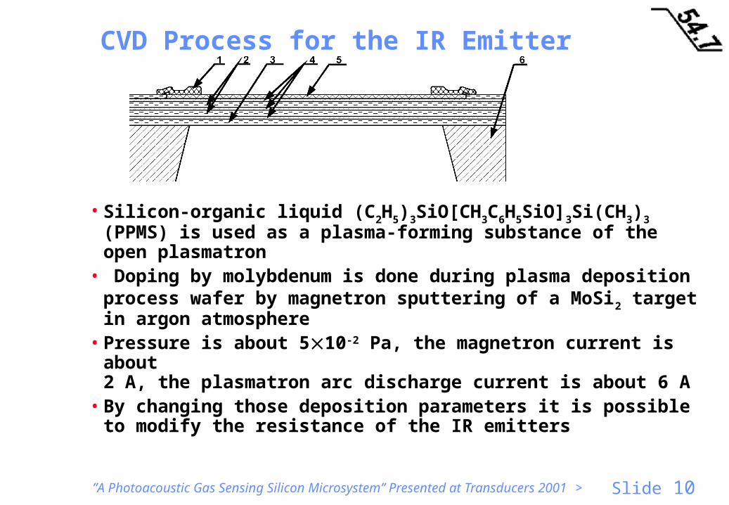
CVD Process for the IR Emitter
• Silicon-organic liquid (C2H5)3SiO[CH3C6H5SiO]3Si(CH3)3 (PPMS) is used as a plasma-forming substance of the open plasmatron
• Doping by molybdenum is done during plasma deposition process wafer by magnetron sputtering of a MoSi2 target in argon atmosphere
• Pressure is about 510-2 Pa, the magnetron current is about 2 A, the plasmatron arc discharge current is about 6 A
• By changing those deposition parameters it is possible to modify the resistance of the IR emitters

”A Photoacoustic Gas Sensing Silicon Microsystem” Presented at Transducers 2001 > Slide 11
Principle of a Microsystem based Photoacoustic Gas Sensing Cell (Early Prototype)
• The photoacoustic sensing microsystem is enabled by packaging a silicon micromachined acoustic pressure sensor chip in a transistor package
10.0 mm
TO-header
IR radiation
4.0 mm
Silicon micromachinedacoustic pressure
sensor chip
Target gas
WindowAbsorptionchamber
Transistor cap

”A Photoacoustic Gas Sensing Silicon Microsystem” Presented at Transducers 2001 > Slide 12
Principle of the Silicon Microphone used in the Gas Sensing Cell (Early Prototype)
• Integrated pressure equalising channel• The diaphragm can have a centre boss structure to increase linearity
Target gas
Al coatingPressure equalising channel
TO-header
Piezo resistors
Sensor chip
Support chip
Window

”A Photoacoustic Gas Sensing Silicon Microsystem” Presented at Transducers 2001 > Slide 13
Silicon Microphone Prototype (Q3/2000)
• Designed by SINTEF and 54.7
• Piezoresistive with centre boss structure
• Manufactured by SensoNor with their Europractice/NORMIC multiproject wafer foundry services
”A Photoacoustic Gas Sensing Silicon Microsystem” Presented at Transducers 2001 > Slide 14
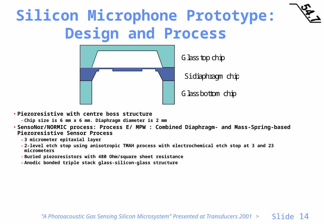
Silicon Microphone Prototype: Design and Process
• Piezoresistive with centre boss structure– Chip size is 6 mm x 6 mm. Diaphragm diameter is 2 mm
• SensoNor/NORMIC process: Process E/ MPW : Combined Diaphragm- and Mass-Spring-based Piezoresistive Sensor Process
– 3 micrometer epitaxial layer– 2-level etch stop using anisotropic TMAH process with electrochemical etch stop at 3 and 23 micrometers– Buried piezoresistors with 480 Ohm/square sheet resistance– Anodic bonded triple stack glass-silicon-glass structure
Glass top chip
Si diaphragm chip
Glass bottom chip

”A Photoacoustic Gas Sensing Silicon Microsystem” Presented at Transducers 2001 > Slide 15
The 54.7 photoacoustic gas sensing cell design (Q4/2000)
• Cell with silicon or electret microphone– Electret microphones model 9723 from Microtronic used in present prototypes
IR-emitter Microphone
Perforated aluminum tube
IR window or filter
Thermopile or pyroelectric IR reference sensor
90 mm
Target gas
6mm IR radiation Absorption path

”A Photoacoustic Gas Sensing Silicon Microsystem” Presented at Transducers 2001 > Slide 16
Sensor Module Design Q4/2000
• Sensor module with the gas sensing cell mounted on a surface mount printed circuit board with analog and digital electronics for monitoring, control and interface
• Size approximately 70mm x 20mm x 10mm

”A Photoacoustic Gas Sensing Silicon Microsystem” Presented at Transducers 2001 > Slide 17
Preliminary Test of Silicon Microphone versus Electret Microphone
• Comparable signal-to-noise performance
0.00
0.01
0.01
0.02
0.02
0.03
0.04
0.04
0.05
0.05
0.06
0.07
0.07
0.08
0.08
0.09
0.10
0.10
Time (s)
Rel
am
pli
tud
eElectretmicrophone
Siliconmicrophone

”A Photoacoustic Gas Sensing Silicon Microsystem” Presented at Transducers 2001 > Slide 18
Test of the DLC IR Emitters
• Power efficiency about 0.1

”A Photoacoustic Gas Sensing Silicon Microsystem” Presented at Transducers 2001 > Slide 19
IR Emitters: Radiation Spectrum
Useful IR spectrum from around 1 to around 10 micrometers

”A Photoacoustic Gas Sensing Silicon Microsystem” Presented at Transducers 2001 > Slide 20
Main characteristics of the IR Emitters• Resistance value: Nominal 55, from 35 to 125 Ohms• Supply voltage: From 5 up to 12 V• Power consumption: 0.5 – 1.0 W• Maximum frequency modulation of the emitted
energy: 200 Hz (~100% modulation at 10 Hz)• Working temperature of film resistor: 500-800 oC,
with header temperature not exceeding 70 oC• Warm-up time: < 30 s• The emissivity factor of the emitting surface: ~0.8• Emitting efficiency (=3-14 micrometers): ~10%• Life time: Mean Time Between Failure (MTBF) of
more than 25 000 hours (more than 3 years)

”A Photoacoustic Gas Sensing Silicon Microsystem” Presented at Transducers 2001 > Slide 21
Preliminary experimental results of CO2 module prototype
Graph of 15 hours measurement (one sample per minute) Lab test: Increased CO2 at start and at inspection. Resolution around 0.3 ppm. Accuracy around ±10ppm?
0 200 400 600 8000.986
0.988
0.99
0.992
0.994
0.996
0.998
1
Temp
Vref
Vref-temp-c
Vg
Vg-temp-c
Vg-temp-ref-c
0.002 approximately:25 ppm CO2
1 oC

”A Photoacoustic Gas Sensing Silicon Microsystem” Presented at Transducers 2001 > Slide 22
Conclusions, further work and acknowledgements• The concept is promising for commercialisation
• Low cost, high selectivity, and high sensitivity can be achieved– Example: CO2 measured with around 10 ppm accuracy and 0.3 ppm resolution
• Potential show stoppers• Long term drift and thermal effects
– Example: Some thermal effects are yet to be understood and minimised
• Further work• Long term stability need to be verified further• Thermal effects will need to be investigated, reduced and compensated• Low cost microsystem production technology need to be further developed
• Many thanks to my coauthors• Dr. Martin Lloyd of Farside Technology is thanked for his
contribution on the digital electronics and the software• Dr. Henrik Rogne and Dag T. Wang of SINTEF are acknowledged
for the design of the silicon microphone