Embed Size (px)
Citation preview

A Novel Clock Distribution A Novel Clock Distribution and Dynamic De-skewing and Dynamic De-skewing
MethodologyMethodology
Arjun Kapoor – University of Colorado at BoulderArjun Kapoor – University of Colorado at BoulderNikhil Jayakumar – Texas A&M University, College StationNikhil Jayakumar – Texas A&M University, College Station
Sunil P. Khatri – Texas A&M University, College StationSunil P. Khatri – Texas A&M University, College Station
IntroductionIntroduction
Clock Distribution critical in ICs.Clock Distribution critical in ICs. In typical ICs, clock is distributed to several sites In typical ICs, clock is distributed to several sites
on the IC from one central clock signal.on the IC from one central clock signal. Requirement is to minimize skew between these Requirement is to minimize skew between these
sites.sites. One of the available networks – H-TreeOne of the available networks – H-Tree
Zero skew without considering process variationsZero skew without considering process variations
With diminishing feature size, increasing die size, With diminishing feature size, increasing die size, intra-die variations lead to increased skew across intra-die variations lead to increased skew across a die.a die.
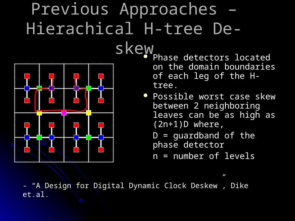
Previous Approaches – Previous Approaches – Hierachical H-tree De-skewHierachical H-tree De-skew
Phase detectors located on Phase detectors located on the domain boundaries of the domain boundaries of each leg of the H-tree.each leg of the H-tree.
Possible worst case skew Possible worst case skew between 2 neighboring between 2 neighboring leaves can be as high as leaves can be as high as (2n+1)D where,(2n+1)D where,D = guardband of the D = guardband of the phase detectorphase detectorn = number of levelsn = number of levels
- “A Design for Digital Dynamic Clock Deskew”, Dike et.al.

Previous Approaches – Previous Approaches – Mesh DeskewMesh Deskew
Phase detectors used Phase detectors used between each pair of leaf between each pair of leaf nodes of the H-tree.nodes of the H-tree.
Clock skew between Clock skew between neighboring leaves is now = D neighboring leaves is now = D (guardband of phase (guardband of phase detector).detector).
Clock skew across die is still Clock skew across die is still high - high - mD between any 2 leaf nodes mD between any 2 leaf nodes where, m = number of phase where, m = number of phase detectors between the 2 leaf detectors between the 2 leaf nodesnodes
- “A Design for Digital Dynamic Clock Deskew”, Dike et.al.

Our ApproachOur Approach
Clock signal is returned Clock signal is returned from leaf nodes.from leaf nodes.
Single phase detector at Single phase detector at center of tree.center of tree.
All returned clock signals All returned clock signals are compared with the are compared with the same delayed reference same delayed reference signal.signal.
De-skewing can be done at De-skewing can be done at boot-up time or dynamically boot-up time or dynamically during free cycles.during free cycles.

Our ApproachOur Approach
Use a modified buffered H-tree.Use a modified buffered H-tree.Have buffers at each level.Have buffers at each level.
Not typically done due to process variation in Not typically done due to process variation in buffers.buffers.
Wire width sizing reversed.Wire width sizing reversed.Typical H-tree – width decreases with level.Typical H-tree – width decreases with level.Our H-tree – width increases with level to make Our H-tree – width increases with level to make
sure buffer at each level sees same load.sure buffer at each level sees same load.
We utilize clock shield wires and We utilize clock shield wires and one one phase phase detector. detector.

Network TopologyNetwork Topology
• Clock assumed to be routed on metal 6.
•Typical H-tree requires clock wire and 2 shield wires on either side.
•We use an additional return wire of same width as clock wire.

The H-TreeThe H-Tree
• Each section of the H-tree has tri-stateable inverters in both the forward and return clock networks.
•Forward network – always ON.
•Return network – only sections on path to be deskewed turned ON.

Wire WidthsWire Widths
• Traditional H-tree: Wire widths larger at center, narrower near leaf nodes – necessary to ensure clean signals at leaf nodes.
•Our H-tree: Wire widths larger near leaf nodes and narrower at center – to ensure each buffer sees same load.
Sizes(in microns) derived for 20mm x 20mm die.
1GHz targeted clock frequency.
LevelLevel
Traditional H-treeTraditional H-tree Our clock treeOur clock tree
LengthLength WidthWidth LengthLength WidthWidth
11 50005000 5050 50005000 1.51.5
22 50005000 2020 50005000 1.51.5
33 25002500 66 25002500 33
44 25002500 33 25002500 33
55 12501250 1.51.5 12501250 66
66 12501250 1.51.5 12501250 66

Deskewing OperationDeskewing Operation
We use only We use only one one phase detector unlike phase detector unlike previous deskewing methods.previous deskewing methods.
Clock signal returned from each node Clock signal returned from each node compared with a single reference signal.compared with a single reference signal.Single phase detector at chip centerSingle phase detector at chip centerLargest skew (after deskewing) between any 2 Largest skew (after deskewing) between any 2
nodes is not a function of the phase detector – nodes is not a function of the phase detector – phase detector accuracy/guardband unimportant.phase detector accuracy/guardband unimportant.
Required delay achieved using tune-able Required delay achieved using tune-able capacitor bank.capacitor bank.

Deskewing OperationDeskewing Operation
Deskewing performed at slower clock rateDeskewing performed at slower clock rateSlower clock required for phase detector to Slower clock required for phase detector to
work.work.Minimize cross-talk Minimize cross-talk
When clock signal returns on return path, forward When clock signal returns on return path, forward path should be stable.path should be stable.
Ensure that half the time period of the clock > Ensure that half the time period of the clock > round trip delay of the clock signal.round trip delay of the clock signal.
Return path is grounded (acts as shield) Return path is grounded (acts as shield) during non-deskew modeduring non-deskew mode

Tune-able Bank at Leaf NodesTune-able Bank at Leaf Nodes
Capacitors are binary Capacitors are binary weighted to facilitate weighted to facilitate precise control of delay.precise control of delay.
Resistor added to Resistor added to increase the incremental increase the incremental delay per capacitor. delay per capacitor.
Value of resistor chosen Value of resistor chosen such that slew rate of last such that slew rate of last segment is not segment is not appreciably changed and appreciably changed and incremental delay is as incremental delay is as desired.desired.

The Phase detectorThe Phase detector
• Condition LAG: O is low at T1 and high at T2 -> A lags B, phase detector not tripped.
• Phase detector said to be tripped when condition LAG does not hold.
• Delay is incrementally increased till the LAG condition FAILS to hold (phase detector trips).
• Guardband of phase detector is hence unimportant

Communicating with Tune-able Communicating with Tune-able Banks and Tri-stateable Buffers.Banks and Tri-stateable Buffers.
Use a 2 wire serial communication scheme.Use a 2 wire serial communication scheme. Use shift registers at each tune-able bank, tristate-Use shift registers at each tune-able bank, tristate-
able buffer.able buffer. At most 6 bits required to address each tristate-able At most 6 bits required to address each tristate-able
node of a 6 level H-tree network.node of a 6 level H-tree network. 7 bits required for a 7 bit capacitor bank.7 bits required for a 7 bit capacitor bank. First assert reset signal (derived from the signal First assert reset signal (derived from the signal
wires) – then send a 6 bit address (to address the wires) – then send a 6 bit address (to address the correct capacitance bank, return path). Next send 7-correct capacitance bank, return path). Next send 7-bit data (capacitance value)bit data (capacitance value)

Addressing MechanismAddressing Mechanism
0 1
00
10 11
01
010
000
110
100
011
001
111
101
3-level H-tree
up, right = 1up, right = 1 down, left = 0 down, left = 0

m-bit Decoder to Address the m-bit Decoder to Address the Tristate-able BuffersTristate-able Buffers
Serial shift registers serially shift in ‘m’ bits of the address (m is the level in the H-tree at which the tri-state buffer is located).Serial shift registers serially shift in ‘m’ bits of the address (m is the level in the H-tree at which the tri-state buffer is located). Clocking stopped by last Flip-flop.Clocking stopped by last Flip-flop. Combinational logic checks if the m-bits in the shift register match the address of the tri-state buffer.Combinational logic checks if the m-bits in the shift register match the address of the tri-state buffer. HIT signal generated if all m-bits are in and address is a matchHIT signal generated if all m-bits are in and address is a match

7-bit Decoder for Selecting 7-bit Decoder for Selecting Capacitance ValueCapacitance Value
Data shifted in serially (similar to the scheme used to address the tri-state buffers).Data shifted in serially (similar to the scheme used to address the tri-state buffers). HIT signal from the decoder of the last tristate-able buffer produces a reset pulseHIT signal from the decoder of the last tristate-able buffer produces a reset pulse Clocking stopped by last Flip-flop (let go again only when the next HIT signal arrives).Clocking stopped by last Flip-flop (let go again only when the next HIT signal arrives).

Overall Operation of the Serial Overall Operation of the Serial Communication SchemeCommunication Scheme
Follow the sequence of:Follow the sequence of:
Serial-reset – transmit address – transmit-data Serial-reset – transmit address – transmit-data sequencesequence
Each such sequence requires 13 clock cyclesEach such sequence requires 13 clock cycles Each leaf node requires at most 2Each leaf node requires at most 277 (for a 7-bit (for a 7-bit
capacitor bank) such sequences.capacitor bank) such sequences. With deskew done at 100Mhz, a 6-level H-tree With deskew done at 100Mhz, a 6-level H-tree
(64 leaf nodes) would be deskewed in about (64 leaf nodes) would be deskewed in about 1ms.1ms.

Experimental ResultsExperimental Results
Initial Skew 115 ps After dynamic de-skew skew reduced to 3ps
Simulated process variations (tSimulated process variations (toxox,,µµ, l, leffeff, V, VTT) ) - values as suggested by:- values as suggested by: “ “Characterization and modelling of clock skew with process Characterization and modelling of clock skew with process
variations”, Zarkesh-Ha et.al.variations”, Zarkesh-Ha et.al.

…….Experimental Results.Experimental Results Compared against traditional (non-buffered) H-tree Compared against traditional (non-buffered) H-tree
with no deskew mechanism (operating at 1Ghz).with no deskew mechanism (operating at 1Ghz). 7.9% lower power in our network7.9% lower power in our network
Many small buffers used.Many small buffers used. Wire loads involved are smaller (improvement would be higher Wire loads involved are smaller (improvement would be higher
for higher frequencies).for higher frequencies).
CategoryCategory Orig. AreaOrig. Area Our AreaOur Area Ovh.Ovh.
WiringWiring 1.635x101.635x1066 2.21x102.21x1066 34.86%34.86%
Central Ck Central Ck DriverDriver 480480 ––
24.56%24.56%
RegeneratorsRegenerators 1843218432 1843218432
TS invertersTS inverters –– 44084408
TS controllersTS controllers –– 307307
CapacitanceCapacitancecontrollerscontrollers –– 410410
CapacitorsCapacitors –– 48804880

ConclusionsConclusions
We have a novel clock distribution network We have a novel clock distribution network with dynamic de-skewing capabilitywith dynamic de-skewing capability
We can de-skew nodes that are skewed We can de-skew nodes that are skewed by 300ps down to 3psby 300ps down to 3ps
We do this with a 7.9% power reduction We do this with a 7.9% power reduction and 34% area overhead when compared and 34% area overhead when compared to a traditional H-treeto a traditional H-tree

Thank you.Thank you.