Embed Size (px)
Citation preview

IOSR Journal of VLSI and Signal Processing (IOSR-JVSP)
ISSN: 2319 – 4200, ISBN No. : 2319 – 4197 Volume 1, Issue 3 (Nov. - Dec. 2012), PP 13-26 www.iosrjournals.org
www.iosrjournals.org 13 | Page
A Novel Approach for High Speed and Low Power 4-Bit
Multiplier
1P.S.H.S.Lakshmi,
2S.Rama Krishna,
3K.Chaitanya
1Assistant Professor, Department Of E.C.E, Sri Chaitanya Engineering College, Visakhapatnam, India. 2Assistant Professor, Department Of E.C.E, Vizag Institute Of Technology Visakhapatnam, India.
2Assistant Professor, Department Of E.C.E, GITAM University, Visakhapatnam, India.
Abstract: A circuit design for a new high speed and Low Power 4-bit Braun Multiplier is presented. The
multiplier is implemented by using different power reduction techniques. To design a multiplier it is necessary
to design an AND gate and Full Adder circuit using the power reduction techniques is presented. The design
uses CMOS digital circuits in order to reduce the power dissipation while maintaining computational
throughput. This paper presents an accurate method of simulating the power dissipation, delay and power
delay product, using different techniques in 250nm technology with supply voltage is 2.5v. The power
dissipation of nearly 41% and delay 26% has been reduced by using modified proposed technique with good
voltage swing levels.
Keywords: A low-power 4-bit Braun multiplier, power reduction techniques.
I. Introduction Multiplication is one of the most important operations in digital computer systems because the
performance of processors is significantly influenced by the speed of their multipliers and adders. Multiplier
plays an important role in the image processor, and sound processor. High performance multiplier is the
important part of the CPU and DSP. Multiplier is one of the most important parameter to determine the
processor’s speed. So, designing of multipliers are essential in Very Large Scale Integration (VLSI) systems
and Digital Signal Processing (DSP) architectures applications.
Building of low power VLSI system has emerged significant performance goal because of the fast
technology in computation. Digital circuit designers have always been encountered in a tradeoff between speed and power consumption to improve their design's performance. The continuing decrease in feature size of
CMOS circuits and corresponding increase in chip density and operating frequency have made power
consumption a major concern in VLSI design. Different types of multipliers have been proposed earlier like
Array Multiplier, Tree Multiplier, and Braun Multiplier.
In this thesis we proposed a new high speed and Low Power 4-bit Braun Multiplier. The multiplier is
implemented by using different power reduction techniques. To design a multiplier it is necessary to design an
AND gate and Full Adder circuit using the power reduction techniques.
The proposed high speed and Low Power 4-bit Braun Multiplier was done using Tanner tools in 250nm
technology with supply voltage is 2.5v.The implementation of low high speed and Low Power 4-bit Braun
Multiplier using various power reduction techniques are done. The power dissipation of nearly 41% has been
reduced by using modified proposed technique with good voltage swing levels In this the implementation technique of several types of adders and study their characteristics and
performance. These are
a) Ripple carry adder or carry propagate adder
b) Carry look-ahead adder
c) Manchester chain adder
d) Carry select adders
e) Carry save Adder
f) Pipelined parallel adder
For the same length of binary number, each of the above adders has different performance in terms of Delay,
Area, and Power.
The most basic arithmetic operation is the addition of two binary digits, i.e. bits. A combinational circuit that adds two bits, according the scheme outlined below, is called a half adder. A full adder is one that
adds three bits, the third produced from a previous addition operation. One way of implementing a full adder is
to utilizes two half adders in its implementation. These Adders can be implemented by using different logic
families.

A Novel Approach For High Speed And Low Power 4-Bit Multiplier Design
www.iosrjournals.org 14 | Page
In this paper Section-2 explains about different logic families, Section-3 gives the information about
implementation of Full adders, Section-4 describes about Multiplier Introduction, Section-5 gives the
information about Static power reduction techniques, In Section-6 we can observe the simulation results for
AND gates, Full adders and multipliers. In Section-7 we can observe the comparisons between different
Multipliers; in Section-8 we can observe the graphical representations of power, delay for Full adders and
multipliers using different power reduction techniques.
II. Different Logic Families 2.1. PMOS vs. NMOS:
N-channel MOSFETs have some inherent performance advantages over p-channel MOSFET’s. The
mobility of electrons, which are carriers in the case of an n-channel device, is about two times greater than that
of holes, which are the carriers in the p-channel device [2].
Thus an n-channel device is faster than a p-channel device. However, PMOS circuits have following
advantages:
PMOS technology is highly controllable
It is a low cost process
It has good yield and high noise immunity.
In addition to inherent fast speed properly, NMOS device also have following advantages. Since
electron mobility is twice (say) that of hole mobility[4], an n-channel device will have one-half the on-
resistance or Impedance of an equivalent p-channel device with the same geometry and under the same
operating conditions. Thus n-channel transistors need only half the size of p-channel devices to achieve the
same impedance. Therefore, n-channel ICs can be smaller for the same complexity or, even more important;
they can be more complex with no increase in silicon area. NMOS circuits offer a speed advantage over PMOS
due to smaller junction areas. Since the operating speed of an MOS IC is largely limited by internal RC time
constants and capacitance of diode is directly proportional to its size, an n-channel junction can have smaller capacitance. This, in turn, improves its speed.
2.2 CMOS:
Complementary metal-oxide-semiconductor (CMOS) is a technology for constructing integrated
circuits. CMOS technology is used in microprocessors, microcontrollers, static, and other digital logic circuits.
CMOS technology is also used for several analog circuits such as image sensors (CMOS sensor), data
converters, and highly integrated transceivers for many types of communication [1]
CMOS is also sometimes referred to as complementary-symmetry metal–oxide semiconductor The words
"complementary-symmetry" refer to the fact that the typical digital design style with CMOS uses
complementary and symmetrical pairs of p-type and n-type metal oxide semiconductor field effect
transistors (MOSFETs) for logic functions. [2]
2.3 DOMINO LOGIC:
Dynamic logic and especially domino logic could play an important role in -the future integrated
circuits. Domino logic circuits have many advantages such as high speed of operation, minimum used area, low
noise margins, and the most important of all, they offer potential power consumption savings since the overall
gate capacitance is smaller than their static counterparts. For this reason circuit design using domino logic
tends to be a very attractive method for high performance, low-power designs. [4]
In this paper, we introduce a new low power Braun multiplier implementation using domino logic,
which is based on a low voltage swing technique. In section 2 the basic structure of the domino logic is
presented. The proposed low-power design technique for domino logic circuits is explained. The application of
the proposed technique on a Braun multiplier implementation is described.
2.4 STRUCTURE OF THE DOMINO LOGIC GATES:
The basic structure of domino logic is shown in Fig.2.1. It is a non-inverting structure, and consists of
an NMOS transistor network, which implements the required logic function, two transistors (an NMOS and a
PMOS) where the clock signal is applied and synchronizes the operation of the circuit, and a static CMOS
inverter which provides the circuit’s output. [2]

A Novel Approach For High Speed And Low Power 4-Bit Multiplier Design
www.iosrjournals.org 15 | Page
Fig 2.1 Conventional domino logic structure
The period where CLK is low is called the precharge phase. In this phase the internal node, F, is
charged to power supply voltage while the output node, F, is discharged to ground. The period where CLK is
high is called the evaluation phase. In this phase the values of the inputs determine the discharge (F = 0) or not
(F = 1) of the internal node. The inverter in the output of a domino logic circuit is included for several reasons.
First, it is required for proper operation of a chain of domino gates. Second, the internal node F is a weak node,
when the clock is high; the high value on that node is not driven.
III. Design And Implementation Of Full Adder 3.1 Full Adder:
A full adder is a combinational circuit that performs the arithmetic sum of three bits: A, B and a carry
in, C, from a previous addition, Also, as in the case of the half adder, the full adder produces the corresponding
sum, S, and a carry out Co. A full adder maybe designed by two half adders in series as shown in Fig. 3.1.
Fig 3.1 Full Adder
Fig 3.2 Full Adder in Domino Logic
The domino logic full adder is compared with a conventional CMOS full adder. The input capacitance
is about half of the conventional CMOS design, thus achieving higher speed and lower powers dissipation. In fact the transistor count in the domino full adder is 21, whereas in conventional CMOS it is 28 the area
required for domino logic full adder. To compare the full-adder performance between domino and conventional
CMOS, circuit simulations are performed using SPICE at a supply voltage of 2.5V. The simulated worst-case
delay time was measured by using a SPICE submicron technology file, for the domino logic adder and for
conventional CMOS full adders which prove the superiority of the domino logic speed comparing to the
conventional CMOS logic [7-8] as shown in Fig. 3.2.
IV. Multiplier Introduction Multiplier plays an important role in the image processor, and sound processor. High performance multiplier is the important part of the CPU and DSP. The multiplier’s speed usually determines the processor’s
speed. In order to improve the multiplier’s speed, the full custom design flow is needed. [6]
Multiplication is a mathematical operation that at its simplest is an abbreviated process of adding an integer to
itself a specified number of times. A number (multiplicand) is added to itself a number of times as specified by
another number (multiplier) to form a result (product). In elementary school, students learn to multiply by
placing the multiplicand on top of the multiplier[3].

A Novel Approach For High Speed And Low Power 4-Bit Multiplier Design
www.iosrjournals.org 16 | Page
The multiplicand is then multiplied by each digit of the multiplier beginning with their most, Least
Significant Digit (LSD). Intermediate results (partial-products) are placed one atop the other, offset by one
digit to align digits of the same weight. The final product is determined by summation of all the partial-
products. Although most people think of multiplication only in base 10, this technique applies equally to any
base, including binary. Fig.4.1.shows the data flow for the basic multiplication technique just described. Each
black dot represents a single digit. [6]
Fig. 4.1 Basic multiplications
4.1. BRAUN MULTIPLIER:
Consider the multiplication of two unsigned n-bit numbers, where
is the multiplicand and
is the multiplier.
The product can be written as follows:
An array implementation, known as the Braun multiplier is shown in Fig.4.2. multiplier uses the same
array structure to handle 2’s complement multiplication, with some of the partial products replaced by their
complements. The multiplier array consists of (n_1) rows of CSA, in which each row contains (n_1) FA cells.
Each FA in the CSA array has two outputs: the sum bit goes down while the carry bit goes to the lower-left FA.
For an FA in the first row, there are only two valid inputs, and the third input bit is set to 0. Therefore, it can be
replaced by a two-input half-adder. The last row is a ripple adder for carry propagation. In this Letter, we
propose a low-power design for this multiplier[3].
Fig-4.2 Braun Multiplier
V. Static Power Dissipation Reduction Techniques Power dissipation is increasing linearly and the power density increases exponentially, because of the
ever-shrinking size of the integrated circuits as the years go. If this exponential rise in the power density
increases continuously few years later, it may have the same power as that of the nuclear reactor. Such high
power density introduces reliability concerns such as, electro migration, thermal stresses and hot carrier
induced device degradation, resulting in the loss of performance. [5]. Thus, it is evident that the methodologies
for the design of low power digital systems are needed.
Several power reduction techniques are discussed here.
A Novel Approach For High Speed And Low Power 4-Bit Multiplier Design
www.iosrjournals.org 17 | Page
5.1. LOW VOLTAGE SWING TECHNIQUE:
The proposed low power architecture for domino gates is based on a low-swing technique. The output
inverter is as shown in Fig.5.1 replaces the output inverter in the structure of the conventional domino gate. [3]
An Inverter using low voltage swing technique is as shown in Fig.5.1.1.
Fig 5.1 Low power/Low Swing Domino Inverter
Fig5.1.1 Schematic of Inverter using low Voltage Swing Technique
5.2. PASS-TRANSISTOR LOGIC:
A popular and widely-used alternative to complementary CMOS is pass-transistor logic, which
attempts to reduce the number of transistors required to implement logic by allowing the primary inputs to
drive gate terminals as well as source/drain terminals. Which only allow primary inputs to drive the gate
terminals of MOSFETS [2]. To design a Braun Multiplier using Pass-Transistor Logic it is necessary to design an AND gates, and Full Adders. These AND gates and Full adders are placed in Braun multiplier. AND gate
using Pass-Transistor logic is shown in Fig.5.2.
5.2. AND gate using Pass-Transistor Logic
5.3. SLEEP STACK WITH KEEPER TECHNIQUE
In second approach i.e. sleep-stack with keeper, we are combining the three different low power
leakage reduction techniques i.e. sleep transistors , stack approach with keeper as shown in Fig.5.3 [11].
Proposed 4-bit Braun Multiplier is also implemented using sleep stack with keeper technique. For this reason
AND gates and Full Adders are implemented in Sleep Stack with keeper technique and the inverter using Sleep Stack with keeper technique is as sown in Fig.5.3.1 AND gate using Sleep Stack with keeper technique is as
sown in Fig.5.3.2.

A Novel Approach For High Speed And Low Power 4-Bit Multiplier Design
www.iosrjournals.org 18 | Page
Fig 5.3 Sleep Stack with Keeper Technique
FIG 5.3.1 INVERTER USING SLEEP STACK WITH KEEPER TECHNIQUE
FIG 5.3.2 AND GATE USING SLEEP STACK WITH KEEPER TECHNIQUE
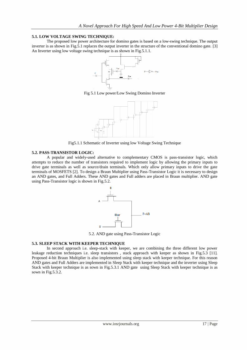
5.4. GALEOR TECHNIQUE:
GALEOR technique reduces the leakage current flowing through the NAND gate for all possible
input combinations by introducing stack effect. GALEOR technique implemented on NAND gate is shown in
the Figure.5.4. In GALEOR technique, a gated leakage NMOS transistor is placed between output and pull-up
circuit and a gated leakage PMOS transistor is placed between output and pull-down circuitry. Transistor states
and stacking effect introduced by the transistors in a GALEOR implemented NAND gate (as shown in Fig
5.4.2) for all possible input combinations is discussed below.[10] When the input vector AB = 00, both the NMOS transistors are turned OFF. This results in a voltage closer to the supply voltage at the node r, which
turns OFF the gated the supply voltage at the node r, which turns OFF the gated leakage PMOS transistor. This
creates a 3 transistor stack to reduce the leakage current flowing through the circuit. When input vector AB =
01 or AB = 10, one of the NMOS and PMOS transistors are turned OFF. Inverter using GALEOR technique is
as shown in Fig 5.4.1.
A Novel Approach For High Speed And Low Power 4-Bit Multiplier Design
www.iosrjournals.org 19 | Page
Fig.5.4. GALEOR Technique
FIG 5.4.1 GALEOR INVERTER
Fig 5.4.2 AND gate using Galeor technique
From the above static power reduction techniques less power dissipation is obtained for Galeor
technique. So, the multiplier is designed by using Galeor technique and compared with the other static power
reduction techniques in 250nm technology with supply voltage is 2.5v using tanner tools. The power
dissipation of nearly 41% has been reduced by using modified proposed technique with good voltage swing
levels.
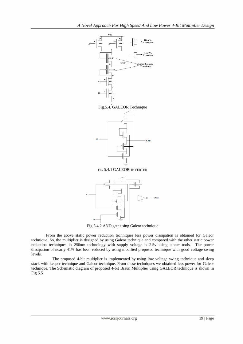
The proposed 4-bit multiplier is implemented by using low voltage swing technique and sleep
stack with keeper technique and Galeor technique. From these techniques we obtained less power for Galeor
technique. The Schematic diagram of proposed 4-bit Braun Multiplier using GALEOR technique is shown in
Fig 5.5
A Novel Approach For High Speed And Low Power 4-Bit Multiplier Design
www.iosrjournals.org 20 | Page
Fig.5.5. Braun Multiplier Schematic using Galeor technique
VI. Simulations And Results This section shows the graphical representations of Inverters, AND gates, Full Adders and Multipliers
using different power reduction techniques.
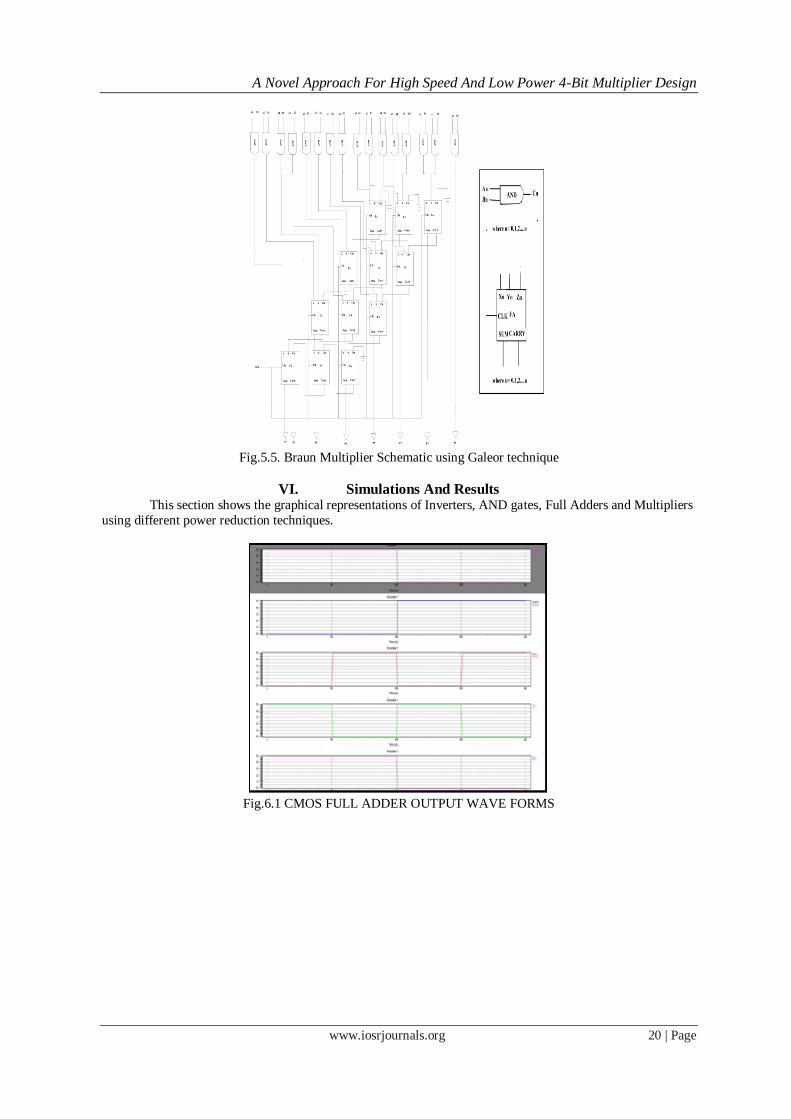
Fig.6.1 CMOS FULL ADDER OUTPUT WAVE FORMS
A Novel Approach For High Speed And Low Power 4-Bit Multiplier Design
www.iosrjournals.org 21 | Page
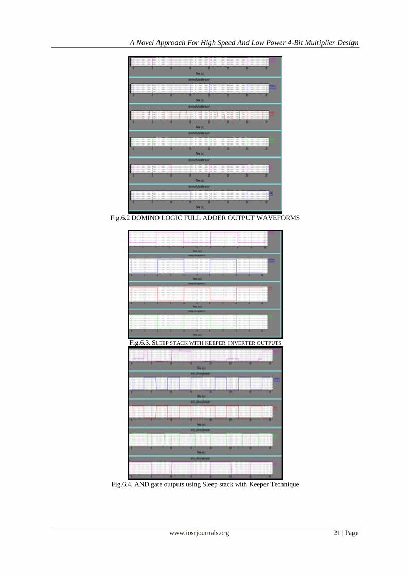
Fig.6.2 DOMINO LOGIC FULL ADDER OUTPUT WAVEFORMS
Fig.6.3. SLEEP STACK WITH KEEPER INVERTER OUTPUTS
Fig.6.4. AND gate outputs using Sleep stack with Keeper Technique
A Novel Approach For High Speed And Low Power 4-Bit Multiplier Design
www.iosrjournals.org 22 | Page
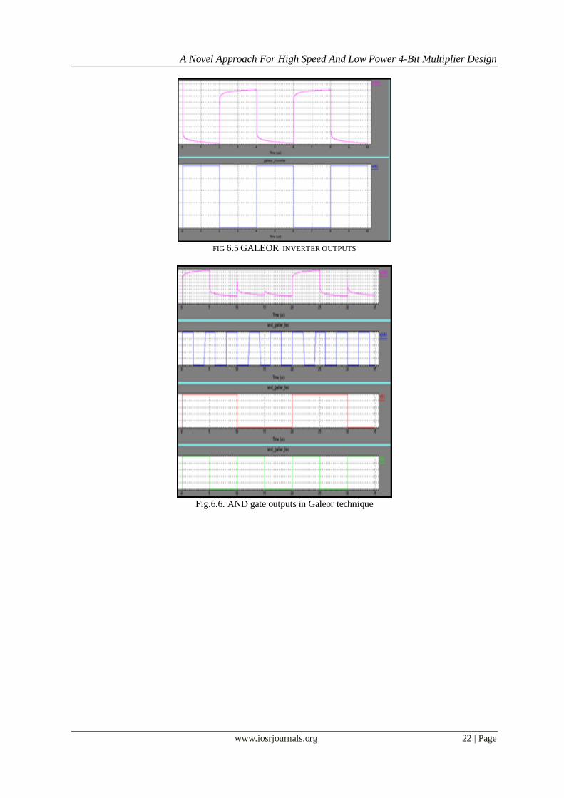
FIG 6.5 GALEOR INVERTER OUTPUTS
Fig.6.6. AND gate outputs in Galeor technique
A Novel Approach For High Speed And Low Power 4-Bit Multiplier Design
www.iosrjournals.org 23 | Page
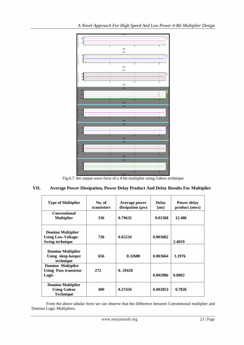
Fig.6.7. the output wave form of a 4-bit multiplier using Galeor technique
VII. Average Power Dissipation, Power Delay Product And Delay Results For Multiplier
Type of Multiplier
No. of
transistors
Average power
dissipation (µw)
Delay
(ms)
Power delay
product (mws)
Conventional
Multiplier
336
0.79632
0.01568
12.486
Domino Multiplier
Using Low-Voltage-
Swing technique
736
0.65234
0.003682
2.4019
Domino Multiplier
Using sleep-keeper
technique
656
0.32688
0.003664
1.1976
Domino Multiplier
Using Pass transistor
Logic
272
0. 29428
0.002986
0.8802
Domino Multiplier
Using Galeor
Technique
400
0.27434
0.002853
0.7826
From the above tabular form we can observe that the difference between Conventional multiplier and
Domino Logic Multipliers.

A Novel Approach For High Speed And Low Power 4-Bit Multiplier Design
www.iosrjournals.org 24 | Page
These Domino Logic Multipliers are implemented by using different power reduction techniques such as Low-
Voltage Swing technique, Sleep-Keeper Technique, Pass-Transistor logic and Galeor Technique. Here the
Conventional Multiplier is implemented by using conventional AND gates and conventional full adders.
Multiplier in Domino Logic is implemented using Low-Voltage-Swing Technique AND gates and Domino
Full Adders.Multiplier in Domino Logic is implemented using AND gates and Full Adders in Sleep-Keeper-
technique. Multiplier in Domino Logic is implemented using Pass-Transistor logic AND gates and Domino
logic Full Adders. Multiplier in Domino Logic is implemented using AND gates, domino full adders in Galeor technique.
VIII. Graphical Representations Of Power & Delay Values
Fig.8.1 Inverter Power Dissipation Using Different Techniques
Fig.8.2 AND Gate Power Dissipation Using Different Power Reduction Techniques
Fig.8.3 Full Adder Power Dissipation Using Different Power Reduction Techniques
Fig.8.4. Proposed 4-Bit Multiplier Power Dissipation Using Different Power Reduction Techniques

A Novel Approach For High Speed And Low Power 4-Bit Multiplier Design
www.iosrjournals.org 25 | Page
Fig.8.5. Inverter Delay Using Different Power Reduction Techniques
Fig.8.6. AND Gate Delay Using Different Power Reduction Techniques
Fig.8.7. Full Adder Delay Using Different Power Reduction Techniques
Fig.8.8. Proposed 4-Bit Multiplier Delay Using Different Power Reduction Techniques

A Novel Approach For High Speed And Low Power 4-Bit Multiplier Design
www.iosrjournals.org 26 | Page
The above graphical representation gives the information about Comparison of proposed 4-bit Braun
Multiplier with the conventional 4-bit Multiplier in terms of Power Dissipation and Delay. It can be observed
from the above graphs from Fig.8.1 to Fig.8.8 for the proposed Multiplier power reduction is 41% and delay
reduction is 26%, when compared with Conventional Multiplier. With these comparisons we can observe that
the low-power & high speed is achieved for 4-bit multiplier using Galeor technique.
IX. Conclusion In this paper we have designed and implemented a new 4-bit Braun Multiplier for low power and high
speed applications. It uses low-voltage swing technique sleepy keeper technique, Galeor technique and Pass-
transistor logic structure, verified by using simulation tools. Power of the circuit can be further reduced by
sizing the transistor using logical effort.
The Main idea of high speed and low power Braun multiplier is to reduce the power dissipation by
using power reduction techniques using Tanner tools 250nm technology and level 49 parameters. It can be
observed that the proposed Multiplier power reduction is 41% and delay reduction is 26%, when compared
with Conventional Multiplier. Hence from these comparisons we can observe that the low-power & high speed is achieved for proposed 4-bit multiplier using Galeor technique when compare to other techniques.
References [1]. N. Weste, and K. Eshraghian, “Principles of CMOS VLSI Design”, Addison-Weslet Publishing company, 1992.
[2]. J. M. Rabaey, M. Pedram, “Low Power Design Methodologies”, Kluwer Academic Publishers, 1996
[3]. Low-Power Domino Logic Multiplier Using Low-Swing Technique A. Rjoub and 0. Koufopavlou 0-7803-5008-
1/98/$10.0001998 IEEE
[4]. K. Roy and S. C. Prasad, “Low-Power CMOS VLSI Circuit Design”, John Wiley &Sons, 1999
[5]. A. P. Chandrakasan, S. Sheng and R. W. Brodersen, “Low Power CMOS Digital Design,” IEEE Journal of Solid-state Circuits,
vol. 27, no. 4, pp. 473-484, April 1999.
[6]. G. H. M. Joordens, J. A. Hegt, and D. M. W. Leenaerts, “A high performance low
voltage switched- current multiplier,” in Proc. IEEE Int. Symp. Circuits and Syst., Apr. 1995, pp. 1856–1859
[7]. S. Hanson, B. Zhai, K. Bernstein, D. Blaauw, A. Bryant, L. Chang, K. K. Das, W. Haensch, E. J. Nowak and D. Sylvester,
“Ultralow-voltage, minimum-energy CMOS,” IBM Journal of Research and development, vol. 50, no. 4-5, pp. 469–490, 2006
[8]. A. P. Chandrakasan, S. Sheng, and R. W. Brodersen, “Low-Power CMOS Digital Design”, IEEE Journal of Solid State Circuits,
vol. 27, pp. 473-483Apr. 1992.
[9]. S. Shah and A. J. Al-Khalili, “Comparison of 32-bit multipliers for various Performance m measures”, 12th International
conference on Microelectronics, Tehran, 2000.
[10]. S. Mutoh et al., “1-V Power Supply High-speed Digital Circuit Technology with Multi-threshold-Voltage CMOS,” IEEE Journal
of Solis-State Circuits, Vol. 30, No. 8, pp. 847-854, August 1995.
[11]. J.C. Park, V. J. Mooney III and P. Pfeiffenberger, “Sleepy Stack Reduction of Leakage Power,” Proceeding of the International
Workshop on Power and Timing Modeling, Optimization and Simulation, pp. 148-158, September 2004.