Embed Size (px)
Citation preview
ELINVO (Electronics, Informatics, and Vocational Education), Mei 2021; vol 6 (1): 26-39
ISSN 2580-6424 (printed), ISSN 2477-2399 (online,) DOI: 10.21831/elinvo.v6i1.40287
A New Two-Switched-Impedance Network for High Ratio Quasi-Z-Source
Inverter
Irham Fadlika1*,2, Mega Agustina1, Rahmatullah Aji Prabowo1,3, Misbahul Munir1, Arif Nur
Afandi1,2 1 Department of Electrical Engineering, State University of Malang, Jalan Semarang 5 Malang, Indonesia 2Centre of Advanced Material for Renewable Energy (CAMRY), State University of Malang, Indonesia
3Adikari Wisesa Indonesia Ltd., East Jakarta, Indonesia
*E-mail: [email protected]
ABSTRACT
The increasing demand and widespread of renewable energy inherently compel the development of power
electronics converter as an interface between consumers and the energy sources. Since the voltage generated on
the typical renewable energy source such photovoltaic is low, the power converter is tasked to transform it to
higher voltage level to meet load or grid voltage demand. This paper presents a new two-switched-impedance
networks qZSI converter called High Ratio Two Switched-impedance quasi-Z-Source Inverter (HR2SZ-qZSI).
The modification on the second cell switched-inductance structure allows this topology to achieve higher boost
factor with a lower shoot-through duty ratio applied, compared with the existing two-switched-impedance-based
converter family. This paper also discusses comparative analysis between the previous and the proposed topology:
almost all the devices’ ratings including capacitor and diode voltage, and inductor current ripple are lower than
the preceding relevant two-switched-impedance qZSI family. A small-scale laboratory prototype with 20 V dc
input, 0.1 shoot-through duty cycle, and 0.2 inverter index modulation was designed and tested. The experimental
results which comprise 3.9 boost factor, 0.78 voltage gain, the voltage across capacitors C1, C2, C3, C4, C5 are 32
V, 36 V, 26 V, 33 V, 32 V, respectively; the voltage stress of the diodes Din, D1, D2, D3, D4, D5 are 72 V, 8 V, 38
V, 68 V, 36 V, 36 V, respectively; and the current ripple of inductors L1, L2, L3, L4 are 0.15 A, 0.08 A, 0.13 A,
0.13 A, respectively, corroborate the theoretical analysis and the HR2SZ-qZSI operation.
Keywords: quasi-Z-Source Inverter (qZSI), voltage gain, boost factor, inductor current ripple, voltage stress
INTRODUCTION
In recent year, the potential for developing
renewable energy is gaining full attention
because of its abundant and non-polluting
energy availability [1]–[9], especially wind and
photovoltaic (PV) energy in which their installed
capacity have reached 733 GW and 707 GW by
end of 2020, respectively [10], [11]. PV, in
particular, is attracting massive demand in
commercial and residential applications
globally. Unfortunately, the dc voltage generated
by this energy source is very low and is highly
dependent on the level of solar irradiation. In the
case of AC mains connection, additional devices
are needed which generally consist of a dc-dc
converter and inverter [12]–[17]. The dc-dc
boost converter is traditionally used to first
convert the input low dc voltage to sufficient
high dc voltage needed for the inverter to
subsequently transform it to ac voltage required
by AC grid. The major drawbacks of this
configuration are it requires separate regulation
of the boost converter and inverter which adds
and complicates the control circuitry, the
conventional Voltage Source Inverter (VSI) only
works in buck mode (step down operation) and
necessitates delay time for each of the leg in
switching operation to prevent short circuit. In
another grid-connected arrangement [16], PV
generators are directly connected with both VSI
and line transformer. As mentioned before, the
traditional VSI limits the attainable output
voltage therefore it requires the size and the turn
of the transformer to adjust with the grid
specification. This condition worsens the overall

I. Fadlika, M. Agustina, R.A. Prabowo, A. N. Afandi, A New Two-Switched Impedance… 27
performance of the power conversion system
since the larger requirement of the 50/60 Hz line
transformer, the bigger the dimension and cost it
required.
Impedance Source Inverter or so-called Z-
Source Inverter (ZSI) has emerged in the past
years as a viable solution to overcome the
practical difficulties mentioned earlier in
renewable energy generation systems [18]. This
converter consists of an X-shaped LC-
impedance network and traditional VSI. It
exhibits many superiorities over the old-
fashioned use of boost dc-dc converter and line
transformer since ZSI can operate in a single
power conversion stage, it also enables the short
circuit or shoot-through operation on each
inverter’s leg which additionally provide the
boosting capability of the low dc voltage.
Moreover, single-stage power conversion of ZSI
can nullify the additional control needed in the
previous classic dc-dc and dc-ac converter
configuration.
Nevertheless, there are some downsides of
the ZSI utilization which encompass the
substantial amount of voltage stress across the
capacitor, the discontinues input current owing
to the series connection of input dc voltage with
the power diode, and since the modulation index
of the inverter is restricted to the value of the
shoot-through duty cycle, the overall dc-ac
voltage gain is also limited. As an effort to
improve the performance operability of ZSI,
quasi-Z-Source Inverter (qZSI) has been derived
[19]. This topology modification includes
categorical features which allow the dc side
current to smoothly flow on account of series
configuration between the dc voltage source and
inductor, lessens the voltage held by the
capacitor, provides one-point ground reference
between the dc source and the converter, and
limits start-up inrush current. These merits
emphasize the further use of qZSI favorably in
PV electricity generation [20]–[27]. Still,
regarding high voltage conversion demand, qZSI
offers no improvement from the former ZSI
topology.
Subsequent adjustments are reported over
the years to gradually improve the qZSI
performance. Switched-inductor (SL) boost
cells, as succeeded previously in ZSI [28], are
adopted in qZSI, namely SL-qZSI and cSL-qZSI
[29], [30]. Owing to the inclusion of the SL boost
networks, these converters have successfully
improved the boost capability of the traditional
qZSI. Another interesting approach is revealed
in [31]. The proposed converter Enhanced Boost
qZSI or called EB-qZSI shifts the inductors and
diodes position and replace one of the inductors
in the two SL cells with a capacitor, hence
realizes higher voltage conversion. A year after,
for the dual purposes of the battery-PV
application, for instance, two symmetrical
structure converters are proposed, Embedded
Switched-Inductor qZSI (ESL-qZSI) and
improved Embedded Switched-Inductor qZSI
(iESL-qZSI) [32]. Two dc sources are attached
inside in each of the switched-impedance
networks to maintain the continuous current
flow across both sources. Yet, it is difficult to
produce and control equally balanced dc input
voltage in these two converters. The floating dc
sources also lose the benefit of joint-ground
reference in the previous qZSI, cSL-qZSI, and
EB-qZSI since they need to be properly isolated
before embedded in the impedance networks.
In light of the aforementioned evolution
of qZSI-derived converters, this paper proposes
a new High Ratio Two Switched-Impedance
quasi-Z-Source Inverter (HR2SZ-qZSI). This
converter put forward the new output SL boost
design thus expand the output-input voltage
conversion proportion. The next two sections
will discuss the methodology and the results of
our newly developed converter in detail.
METHODS
This section begins with revisiting the
structures and electrical characteristics of the
previous converter topologies: cSL-qZSI, EB-
qZSI, ESL-qZSI, and iESL-qZSI. Next, the
step-by-step operational procedure of the
proposed HR2SZ-qZSI is thoroughly explained
28 ELINVO (Electronics, Informatics, and Vocational Education), Mei 2021; 6(1): 26-39
and the associated mathematical analysis is
expressed.
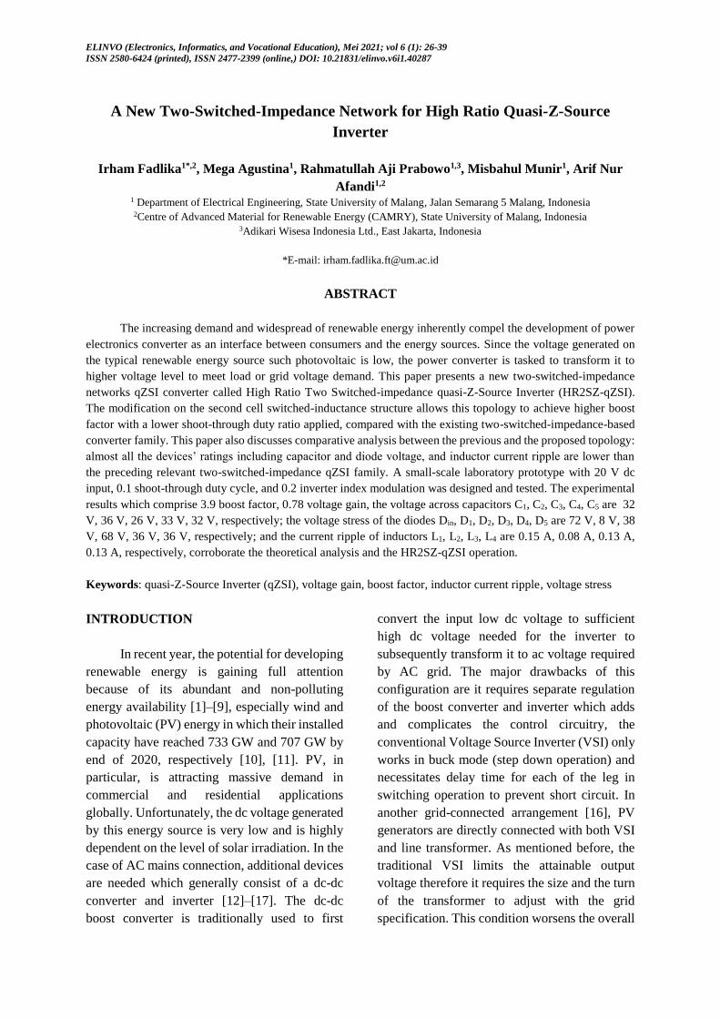
A. cSL-qZSI Topology
The continuous switched-inductor qZSI
(cSL-qZSI) is shown in Fig. 1. According to
[30], the output DC link, boost factor, capacitor
voltage, inductor current ripple, and diode
voltage are defined wherein Vin is a DC source,
D is the value of shoot-through duty ratio, and TS
is switching period.
𝑉𝑜 =
1
1−3𝐷𝑉𝑖𝑛
𝐵 =1
1−3𝐷
(1)
𝑉𝐶1 =
1−𝐷
(1+𝐷)(1−3𝐷)𝑉𝑖𝑛
𝑉𝐶2 =2𝐷
(1+𝐷)(1−3𝐷)𝑉𝑖𝑛
(2)
|∆𝑖𝐿1,𝑃−𝑃| =
(1−3𝐷2)
2𝐿1(1−2𝐷−3𝐷2)𝐷𝑇𝑆𝑉𝑖𝑛
|∆𝑖𝐿2,𝐿4,𝑃−𝑃| =(1−𝐷)
2𝐿2,4(1−2𝐷−3𝐷2)𝐷𝑇𝑆𝑉𝑖𝑛
|∆𝑖𝐿3,𝑃−𝑃| =2𝐷
2𝐿3(1−2𝐷−3𝐷2)𝐷𝑇𝑆𝑉𝑖𝑛
(3)
𝑉𝐷𝑖𝑛 =
(1+𝐷)
(1−2𝐷−3𝐷2)𝑉𝑖𝑛
𝑉𝐷1 =2𝐷2
(1−3𝐷−𝐷2+3𝐷3)𝑉𝑖𝑛
𝑉𝐷2 = 𝑉𝐷5 =𝐷
(1−2𝐷−3𝐷2)𝑉𝑖𝑛
𝑉𝐷3 =2𝐷
(1−2𝐷−3𝐷2)𝑉𝑖𝑛
𝑉𝐷4 =(1−𝐷)
(1−2𝐷−3𝐷2)𝑉𝑖𝑛
𝑉𝐷6 =(1−2𝐷−𝐷2)
(1−3𝐷−𝐷2+3𝐷3)𝑉𝑖𝑛
(4)
Figure 1. Topology of continuous switched-inductor
qZSI (cSL-qZSI)
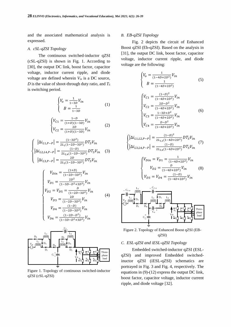
B. EB-qZSI Topology
Fig. 2 depicts the circuit of Enhanced
Boost qZSI (Eb-qZSI). Based on the analysis in
[31], the output DC link, boost factor, capacitor
voltage, inductor current ripple, and diode
voltage are the following:
𝑉𝑜 =
1
(1−4𝐷+2𝐷2)𝑉𝑖𝑛
𝐵 =1
(1−4𝐷+2𝐷2)
(5)
𝑉𝐶1 =
(1−𝐷)2
(1−4𝐷+2𝐷2)𝑉𝑖𝑛
𝑉𝐶2 =2𝐷−𝐷2
(1−4𝐷+2𝐷2)𝑉𝑖𝑛
𝑉𝐶3 =1−3𝐷+𝐷2
(1−4𝐷+2𝐷2)𝑉𝑖𝑛
𝑉𝐶4 =𝐷−𝐷2
(1−4𝐷+2𝐷2)𝑉𝑖𝑛
(6)
|∆𝑖𝐿1,𝐿2,𝑃−𝑃| =
(1−𝐷)2
2𝐿1,2(1−4𝐷+2𝐷2)𝐷𝑇𝑆𝑉𝑖𝑛
|∆𝑖𝐿3,𝐿4,𝑃−𝑃| =(1−𝐷)
2𝐿3,4(1−4𝐷+2𝐷2)𝐷𝑇𝑆𝑉𝑖𝑛
(7)
𝑉𝐷𝑖𝑛 = 𝑉𝐷1 =
1
(1−4𝐷+2𝐷2)𝑉𝑖𝑛
𝑉𝐷2 =𝐷
(1−4𝐷+2𝐷2)𝑉𝑖𝑛
𝑉𝐷3 = 𝑉𝐷4 =(1−𝐷)
(1−4𝐷+2𝐷2)𝑉𝑖𝑛
(8)
Figure 2. Topology of Enhanced Boost qZSI (EB-
qZSI)
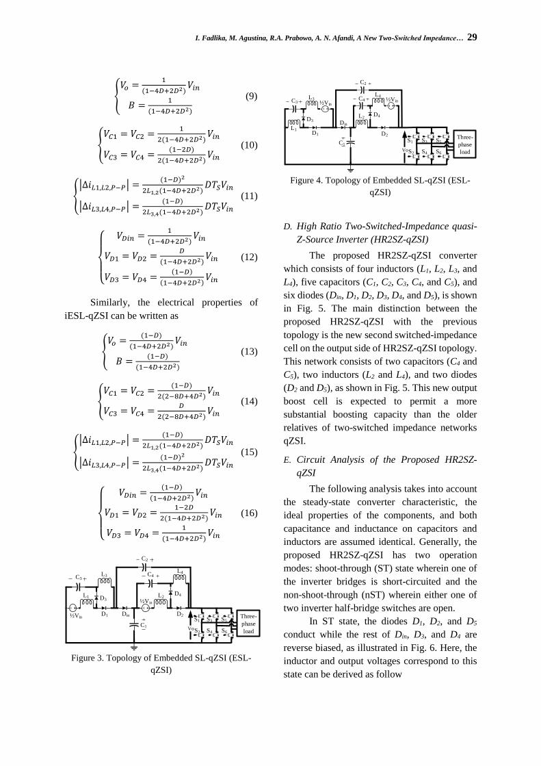
C. ESL-qZSI and iESL-qZSI Topology
Embedded switched-inductor qZSI (ESL-
qZSI) and improved Embedded switched-
inuctor qZSI (iESL-qZSI) schematics are
portrayed in Fig. 3 and Fig. 4, respectively. The
equations in (9)-(12) express the output DC link,
boost factor, capacitor voltage, inductor current
ripple, and diode voltage [32].
C1
C2
D1
L1 L2
D2
L3 L4
D6 D5
D3 D4Vin Din
S1
S2
S3
S4
S5
S6
Three-
phase
loadVo
Vin
L1
D1 Din
L2
D4
D2D3
L3
L4
C4
C2C3
C1
S1
S2
S3
S4
S5
S6
Three-
phase
loadVo
I. Fadlika, M. Agustina, R.A. Prabowo, A. N. Afandi, A New Two-Switched Impedance… 29
𝑉𝑜 =
1
(1−4𝐷+2𝐷2)𝑉𝑖𝑛
𝐵 =1
(1−4𝐷+2𝐷2)
(9)
𝑉𝐶1 = 𝑉𝐶2 =
1
2(1−4𝐷+2𝐷2)𝑉𝑖𝑛
𝑉𝐶3 = 𝑉𝐶4 =(1−2𝐷)
2(1−4𝐷+2𝐷2)𝑉𝑖𝑛
(10)
|∆𝑖𝐿1,𝐿2,𝑃−𝑃| =
(1−𝐷)2
2𝐿1,2(1−4𝐷+2𝐷2)𝐷𝑇𝑆𝑉𝑖𝑛
|∆𝑖𝐿3,𝐿4,𝑃−𝑃| =(1−𝐷)
2𝐿3,4(1−4𝐷+2𝐷2)𝐷𝑇𝑆𝑉𝑖𝑛
(11)
𝑉𝐷𝑖𝑛 =
1
(1−4𝐷+2𝐷2)𝑉𝑖𝑛
𝑉𝐷1 = 𝑉𝐷2 =𝐷
(1−4𝐷+2𝐷2)𝑉𝑖𝑛
𝑉𝐷3 = 𝑉𝐷4 =(1−𝐷)
(1−4𝐷+2𝐷2)𝑉𝑖𝑛
(12)
Similarly, the electrical properties of
iESL-qZSI can be written as
𝑉𝑜 =
(1−𝐷)
(1−4𝐷+2𝐷2)𝑉𝑖𝑛
𝐵 =(1−𝐷)
(1−4𝐷+2𝐷2)
(13)
𝑉𝐶1 = 𝑉𝐶2 =
(1−𝐷)
2(2−8𝐷+4𝐷2)𝑉𝑖𝑛
𝑉𝐶3 = 𝑉𝐶4 =𝐷
2(2−8𝐷+4𝐷2)𝑉𝑖𝑛
(14)
|∆𝑖𝐿1,𝐿2,𝑃−𝑃| =
(1−𝐷)
2𝐿1,2(1−4𝐷+2𝐷2)𝐷𝑇𝑆𝑉𝑖𝑛
|∆𝑖𝐿3,𝐿4,𝑃−𝑃| =(1−𝐷)2
2𝐿3,4(1−4𝐷+2𝐷2)𝐷𝑇𝑆𝑉𝑖𝑛
(15)
𝑉𝐷𝑖𝑛 =
(1−𝐷)
(1−4𝐷+2𝐷2)𝑉𝑖𝑛
𝑉𝐷1 = 𝑉𝐷2 =1−2𝐷
2(1−4𝐷+2𝐷2)𝑉𝑖𝑛
𝑉𝐷3 = 𝑉𝐷4 =1
(1−4𝐷+2𝐷2)𝑉𝑖𝑛
(16)
Figure 3. Topology of Embedded SL-qZSI (ESL-
qZSI)
Figure 4. Topology of Embedded SL-qZSI (ESL-
qZSI)
D. High Ratio Two-Switched-Impedance quasi-
Z-Source Inverter (HR2SZ-qZSI)
The proposed HR2SZ-qZSI converter
which consists of four inductors (L1, L2, L3, and
L4), five capacitors (C1, C2, C3, C4, and C5), and
six diodes (Din, D1, D2, D3, D4, and D5), is shown
in Fig. 5. The main distinction between the
proposed HR2SZ-qZSI with the previous
topology is the new second switched-impedance
cell on the output side of HR2SZ-qZSI topology.
This network consists of two capacitors (C4 and
C5), two inductors (L2 and L4), and two diodes
(D2 and D5), as shown in Fig. 5. This new output
boost cell is expected to permit a more
substantial boosting capacity than the older
relatives of two-switched impedance networks
qZSI.
E. Circuit Analysis of the Proposed HR2SZ-
qZSI
The following analysis takes into account
the steady-state converter characteristic, the
ideal properties of the components, and both
capacitance and inductance on capacitors and
inductors are assumed identical. Generally, the
proposed HR2SZ-qZSI has two operation
modes: shoot-through (ST) state wherein one of
the inverter bridges is short-circuited and the
non-shoot-through (nST) wherein either one of
two inverter half-bridge switches are open.
In ST state, the diodes D1, D2, and D5
conduct while the rest of Din, D3, and D4 are
reverse biased, as illustrated in Fig. 6. Here, the
inductor and output voltages correspond to this
state can be derived as follow
½Vin
L1
D1 Din
½Vin
L2
D2
D4D3
L3L4C4
C2
C3
C1
S1
S2
S3
S4
S5
S6
Three-
phase
loadVo
L1D1
Din
L2
D2
D4D3
L3L4
C4
C2
C3
C1
½Vin½Vin
S1
S2
S3
S4
S5
S6
Three-
phase
loadVo

30 ELINVO (Electronics, Informatics, and Vocational Education), Mei 2021; 6(1): 26-39
𝑉𝐿1(𝑆𝑇) = 𝑉𝑖𝑛+𝑉𝐶2𝑉𝐿2(𝑆𝑇) = 𝑉𝐶1 = 𝑉𝐶5𝑉𝐿3(𝑆𝑇) = 𝑉𝐶2 + 𝑉𝐶3𝑉𝐿4(𝑆𝑇) = 𝑉𝐶5 + 𝑉𝐶4
𝑉𝑜 = 0
(17)
Conversely, the diodes Din, D3, and D4
enter conduction mode and the rest of D1, D2, and
D5 are turned off in NST state, as portrayed in
Fig. 7. Then, expressions of the voltage across
inductors and dc-link are obtained as
𝑉𝐿1(𝑁𝑆𝑇) = 𝑉𝑖𝑛 − 𝑉𝐶3𝑉𝐿2(𝑁𝑆𝑇) = 𝑉𝐶5 − 𝑉𝐶4𝑉𝐿3(𝑁𝑆𝑇) = 𝑉𝐶3 − 𝑉𝐶1𝑉𝐿4(𝑁𝑆𝑇) = 𝑉𝐶4 − 𝑉𝐶2
𝑉𝑂 = 𝑉𝐶1 − 𝑉𝐿2 + 𝑉𝐶5 − 𝑉𝐿4
(18)
Figure 5. The Proposed Topology (HR2SZ-qZSI)
Figure 6. Shoot-through State of HR2SZ-qZSI
Topology
Figure 7. Non-shoot-through State of HR2SZ-qZSI
Topology
After acquiring the inductor voltage
expressions both in ST and NST modes, the
voltage across all capacitors and the dc-link
voltage can be found, as in (19), with aid of the
voltage-second balance principle across all
inductors in one switching period. The
conversion ratio of output dc-link voltage to the
input voltage, namely boost factor (B), is also
derived. The voltage held by the diodes is then
obtained when they are in reverse blocking
mode, as expressed in (20).
𝑉𝐶1 = 𝑉𝐶5 =
(1−𝐷)2
(1−6𝐷+5𝐷2−𝐷3)𝑉𝑖𝑛
𝑉𝐶2 =(1+𝐷−𝐷2)
(1−6𝐷+5𝐷2−𝐷3)𝑉𝑖𝑛
𝑉𝐶3 =(1−4𝐷+2𝐷2)
(1−6𝐷+5𝐷2−𝐷3)𝑉𝑖𝑛
𝑉𝐶4 =(1−𝐷)
(1−6𝐷+5𝐷2−𝐷3)𝑉𝑖𝑛
𝑉𝑜 =(2−𝐷)
(1−6𝐷+5𝐷2−𝐷3)𝑉𝑖𝑛 = 𝐵𝑉𝑖𝑛
𝐵 =(2−𝐷)
(1−6𝐷+5𝐷2−𝐷3)
(19)
𝑉𝐷1 =
𝐷(2−𝐷)
(1−6𝐷+5𝐷2−𝐷3)𝑉𝑖𝑛
𝑉𝐷2 =1
(1−6𝐷+5𝐷2−𝐷3)𝑉𝑖𝑛
𝑉𝐷5 =1−𝐷
(1−6𝐷+5𝐷2−𝐷3)𝑉𝑖𝑛
(20)
𝑉𝐷𝑖𝑛 =
2−𝐷
(1−6𝐷+5𝐷2−𝐷3)𝑉𝑖𝑛
𝑉𝐷3 =(1−𝐷)(2−𝐷)
(1−6𝐷+5𝐷2−𝐷3)𝑉𝑖𝑛
𝑉𝐷4 =1−𝐷
(1−6𝐷+5𝐷2−𝐷3)𝑉𝑖𝑛
(21)
VC1
VC2
VL1
VL2
VL3 VL4
Vin
IL1
IL3
IL2
IL4
Vo
VC5
VC4VC3
VC1
VC2
VL1
VL2
VL3 VL4
Vin
IL1
IL3
IL2
IL4
VC5
VC4VC3
Vo

I. Fadlika, M. Agustina, R.A. Prabowo, A. N. Afandi, A New Two-Switched Impedance… 31
RESULT AND DISCUSSION
A. Analysis of Boost Factor and Voltage Gain
Based on the boost factor on (1), (5), (9),
(13), and (19), we have the comparison graph
between the proposed HR2SZ-qZSI topology
and the previous topology, as shown in Fig. 8.
From Fig. 8, we can know that the boost factor
of the proposed HR2SZ-qZSI is higher than the
previous topology, and to produce that higher
boost factor, the proposed HR2SZ-qZSI
topology uses a lower shoot-through duty ratio.
The simple boost control (SBC) method
on [18] is used to control the shoot-through state
and non-shoot-through state of the proposed
HR2SZ-qZSI topology. We use this method
because the control structure is quite simple
wherein the shoot-through state is created by the
comparison of the two constant voltage that
equal to or greater than the peak value of the
sinewave reference. The restriction of the ST
duty ratio to the modulation index follows
𝐷 = 1 −𝑀 (22)
By substituting the shoot-through duty
ratio (D) on (22) to the boost factor (B) of the
proposed HR2SZ-qZSI on (21), we can define
the boost factor as,
𝐵 =(2−(1−𝑀))
(1−6(1−𝑀)+5(1−𝑀)2−(1−𝑀)3) (23)
On the output inverter side, the peak
voltage of one inverter phase can be written as,
𝑝ℎ = 𝑀𝑉𝑜
2= 𝑀𝐵
𝑉𝑖𝑛
2 (24)
From (24) and (23), we have the relation
of voltage gain as follow
𝐺 =2𝑝ℎ
𝑉𝑖𝑛= 𝑀𝐵 =
𝑀2+𝑀
𝑀3+2𝑀2−𝑀−1 (25)
By modifying the voltage gain of the
previous topology, as shown in (25), then we get
the comparison graph of the voltage gain
between the proposed HR2SZ-qZSI and the
previous topology, as shown in Fig. 9.
According to this figure, we can conclude that
the voltage gain of the proposed HR2SZ-qZSI
topology is higher than the previous topology. In
other words, to achieve the same voltage gain
value as the previous topology, the proposed
HR2SZ-qZSI exert a higher modulation index
value hence the phase inverter voltage waveform
quality can be markedly increased.
B. Capacitor and Diode Voltage Stress Analysis
To properly compare the capacitor and
diode voltage stresses, the ST duty cycle of the
previous converters are matched with the
proposed HR2SZ-qZSI on the same voltage
gain. The corresponding adjustments are listed in
Table 1. Combining each capacitor and diode
voltage equations for all topology, the plots of
their comparison are provided in Fig. 10 and 11,
respectively.
Figure 8. Boost Factor Comparison between the
Proposed HR2SZ-qZSI Topology and the Previous
Topology
Figure 9. Voltage Gain Comparison Between the
Proposed HR2SZ-qZSI Topology and The Previous
Topology

32 ELINVO (Electronics, Informatics, and Vocational Education), Mei 2021; 6(1): 26-39
From Fig. 10, we know that with the same
shoot-through duty ratio, voltage stress on the C1
of the proposed HR2SZ-qZSI is the lowest
among all converters. Similarly, the voltage on
C3 on the proposed topology is the lowest, except
with that of iESL-qZSI. Meanwhile, the voltage
stress on C2 and C4 of the proposed HR2SZ-qZSI
topology is relatively similar to the previous
converters, but higher when compared with C4
voltage on iESL-qZSI.
From Fig. 11, the smallest peak voltage
experienced by the power diode Din and D1 when
in reverse bias are found in the HR2SZ-qZSI.
For D3, D4, and D5, all converters have relatively
equal voltage stress. However, the proposed
HR2SZ-qZSI suffers the highest voltage stress
on D2.
Table 1. The Proposed HR2SZ-qZSI Shoot-through
Duty Ratio Form
Topology Shoot-through Duty Ratio, (D)
DcSL-qZSI D3-4D2+3D+1
D3-2D2-3D+5
DEB-qZSI D3-D2-6D+7-√D6-10D5+45D4-110D3+150D2-108D+33
4D2-12D+8
DESL-qZSI D3-D2-6D+7-√D6-10D5+45D4-110D3+150D2-108D+33
4D2-12D+8
DiESL-qZSI D3-D2-6D+7-√D6-10D5+45D4-110D3+150D2-108D+33
4D2-12D+8
DHR2SZ-
qZSI
(1-D)(2-D)
(1-6D+5D2-D3)
Figure 10. Capacitor voltage stress comparison
between the proposed HR2SZ-qZSI topology and
the previous topology
Figure 11. Diode voltage stress comparison between
the proposed HR2SZ-qZSI topology and the
previous topology
C. Analysis of Inductor Current Ripple
The inductor voltage VLn expression is
given in (26), where n indicates the suitable
inductor position based on the circuit in Fig. 5.
𝑉𝐿𝑛 = 𝐿𝑛𝑑𝑖𝐿𝑛
𝑑𝑡 (26)
The peak-to-peak inductor current or
current ripple is expressed by substituting (26)
and (19) to (17) or (18). Note that the inductor
current rose and fell every half of the switching
frequency thus the absolute value of the inductor
current ripple for both ST and NST states are
identical. The following equations represent the
corresponding absolute ripple on the inductor
currents,
|∆𝑖𝐿1,𝑃−𝑃| =
(2−𝐷)(1−𝐷)2
2𝐿1(1−6𝐷+5𝐷2−𝐷3)
𝐷𝑇𝑆𝑉𝑖𝑛
|∆𝑖𝐿2,𝑃−𝑃| =(1−𝐷)2
2𝐿2(1−6𝐷+5𝐷2−𝐷3)
𝐷𝑇𝑆𝑉𝑖𝑛
|∆𝑖𝐿3,𝑃−𝑃| =(1−𝐷)(2−𝐷)
2𝐿3(1−6𝐷+5𝐷2−𝐷3)
𝐷𝑇𝑆𝑉𝑖𝑛
|∆𝑖𝐿4,𝑃−𝑃| =(1−𝐷)(2−𝐷)
2𝐿4(1−6𝐷+5𝐷2−𝐷3)
𝐷𝑇𝑆𝑉𝑖𝑛
(27)
From those, we get the comparison graph
of the inductor current ripple between the
proposed HR2SZ-qZSI topology with the
previous topology by substituting Dtopology from
Table I into the inductor current ripple on (3),
(7), (11), (15), and (27), as shown in Fig. 12. As
demonstrated in this figure, the proposed

I. Fadlika, M. Agustina, R.A. Prabowo, A. N. Afandi, A New Two-Switched Impedance… 33
HR2SZ-qZSI has the best characteristic since the
current ripples on all the inductors were the
lowest between all relevant two-switched-
impedance-based qZSI.
D. Simulation Results
To clearly understand the operation of the
proposed topology and to test all the previous
associated formulae, circuit simulation based on
Fig. 5 is conducted in PSIM with the parameter
detail is provided in Table 2. The converter is
performed using SBC modulation technique as
previously mentioned in the analysis.
Fig. 13 shows the line voltage, phase
voltage, and phase current waveforms. The value
of filtered peak phase voltage is 380 V and its
rms voltage is 219 V and the load current is
around 4.38 A. The steady state capacitor
voltage waveforms are depicted in the next
figure. We obtain VC1 = VC5 = 165 V, VC2 = 255
V, VC3 = 101 V, and VC4 = 192 V from Fig. 14.
From Fig. 15, the output voltage and diode
voltage are Vo = 421 V, VDin = 420 V, VD4 = VD5
= 193 V, VD1 = 64 V, VD2 = 226 V, and VD3 = 357
V. Both inductor current waveforms and their
ripple are presented in Fig. 16. This figure
delineates the current ripple profile such are
|∆iL1, P-P| = 6.81 A, |∆iL2, P-P| = 3.68 A, and |∆iL3,
P-P| = |∆iL4, P-P| = 8.02 A.
The simulation has offered clarity and
verification of the proposed HR2SZ-qZSI
topology. For instance, according to (19), the
calculated dc-link voltage is 424.62 V and gives
an 8.846 boost factor. According to the
simulation, they are 421 V and 8.77,
respectively. Similar conformities for capacitor
and diode voltage, the phase inverter voltage,
and the current ripple are also found with the
prior mathematical analysis in (20), (21), (24),
and (27).
Figure 12. Current ripple inductor comparison
between the proposed HR2SZ-qZSI topology and
the previous topology
Table 2. Simulation Parameter
No. Parameter Rating
1. DC source, (Vin) 48 VDC
2. Inductor, (L1=L2=L3=L4) 330 µH
3. Capacitor,
(C1=C2=C3=C4=C5) 470 µF
4. Switching frequency, (fs) 10 kHz
5. Inverter frequency (f) 50 Hz
6. Modulation index, (M) 0.85
7. Shoot-through duty ratio,
(D) 0.15
8. Output filter, (Lf and Cf)
1.5 mH, 10
µF
9. Load 50 Ω
Figure 13. Voltage waveforms before and after LC
Output Filter and Phase Current After Filter
Figure 14. Capacitor voltage simulation waveforms
for VC1, VC2, VC3, VC4, and VC5
0
-200
-400
200
400
Line Voltage (Before Filter)
0
-200
-400
200
400
Phase Voltage (After Filter)
1.9 1.91 1.92 1.93 1.94 1.95 1.96
Time (s)
0
-2
-4
2
4
Phase Current (After Filter)
34 ELINVO (Electronics, Informatics, and Vocational Education), Mei 2021; 6(1): 26-39
Figure 15. Simulation waveform of dc-link output
voltage Vo and voltage across diodes VDin, VD1, VD2,
VD3, VD4, and VD5
Figure 16. Simulation result of the inductor currents
and their respective ripples
E. Experimental Results
A small-scale laboratory prototype is built
to examine the practical ability of the proposed
HR2SZ-qZSI. In the experiment, the SBC
modulation method is constructed using
TMS320F28335 microcontroller. Following the
configuration in Fig. 5, the rest of the experiment
detail is given in Table 3. The low modulation
index is regulated at 0.2 to restrict the power
output of the inverter since the low value resistor
of 50 Ω is utilized. Similarly, the input voltage is
scaled down to 20 Vdc instead of 48 Vdc used in
the previous simulation.
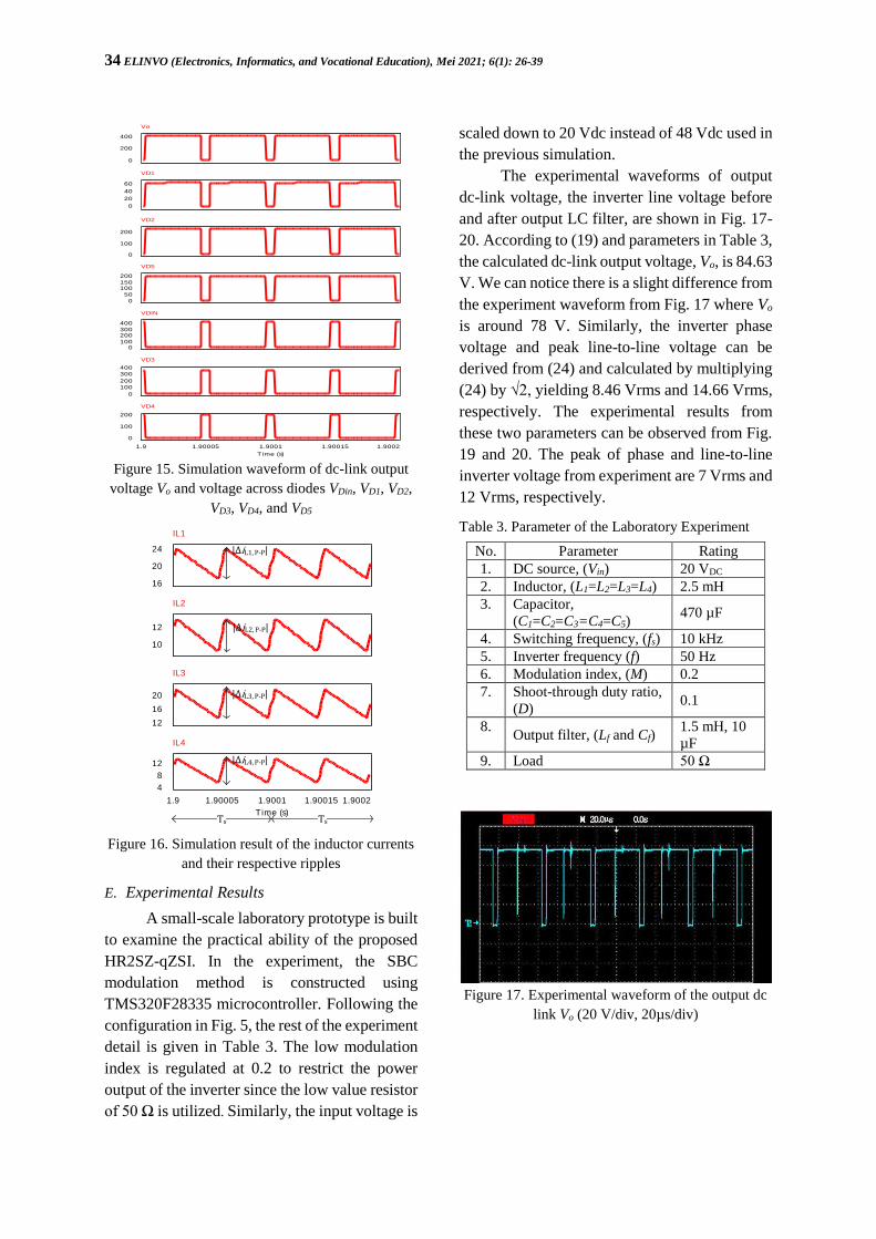
The experimental waveforms of output
dc-link voltage, the inverter line voltage before
and after output LC filter, are shown in Fig. 17-
20. According to (19) and parameters in Table 3,
the calculated dc-link output voltage, Vo, is 84.63
V. We can notice there is a slight difference from
the experiment waveform from Fig. 17 where Vo
is around 78 V. Similarly, the inverter phase
voltage and peak line-to-line voltage can be
derived from (24) and calculated by multiplying
(24) by √2, yielding 8.46 Vrms and 14.66 Vrms,
respectively. The experimental results from
these two parameters can be observed from Fig.
19 and 20. The peak of phase and line-to-line
inverter voltage from experiment are 7 Vrms and
12 Vrms, respectively.
Table 3. Parameter of the Laboratory Experiment
No. Parameter Rating
1. DC source, (Vin) 20 VDC
2. Inductor, (L1=L2=L3=L4) 2.5 mH
3. Capacitor,
(C1=C2=C3=C4=C5) 470 µF
4. Switching frequency, (fs) 10 kHz
5. Inverter frequency (f) 50 Hz
6. Modulation index, (M) 0.2
7. Shoot-through duty ratio,
(D) 0.1
8. Output filter, (Lf and Cf)
1.5 mH, 10
µF
9. Load 50 Ω
Figure 17. Experimental waveform of the output dc
link Vo (20 V/div, 20µs/div)
0
200
400
Vo
0
20
40
60
VD1
0
100
200
VD2
0
50
100150
200
VD5
0100
200300
400
VDIN
0
100
200
300
400
VD3
1.9 1.90005 1.9001 1.90015 1.9002
Time (s)
0
100
200
VD4
16
20
24
IL1
10
12
IL2
12
16
20
IL3
1.9 1.90005 1.9001 1.90015 1.9002
Time (s)
4
8
12
IL4
Ts Ts
|∆iL4, P-P|
|∆iL3, P-P|
|∆iL2, P-P|
|∆iL1, P-P|
I. Fadlika, M. Agustina, R.A. Prabowo, A. N. Afandi, A New Two-Switched Impedance… 35
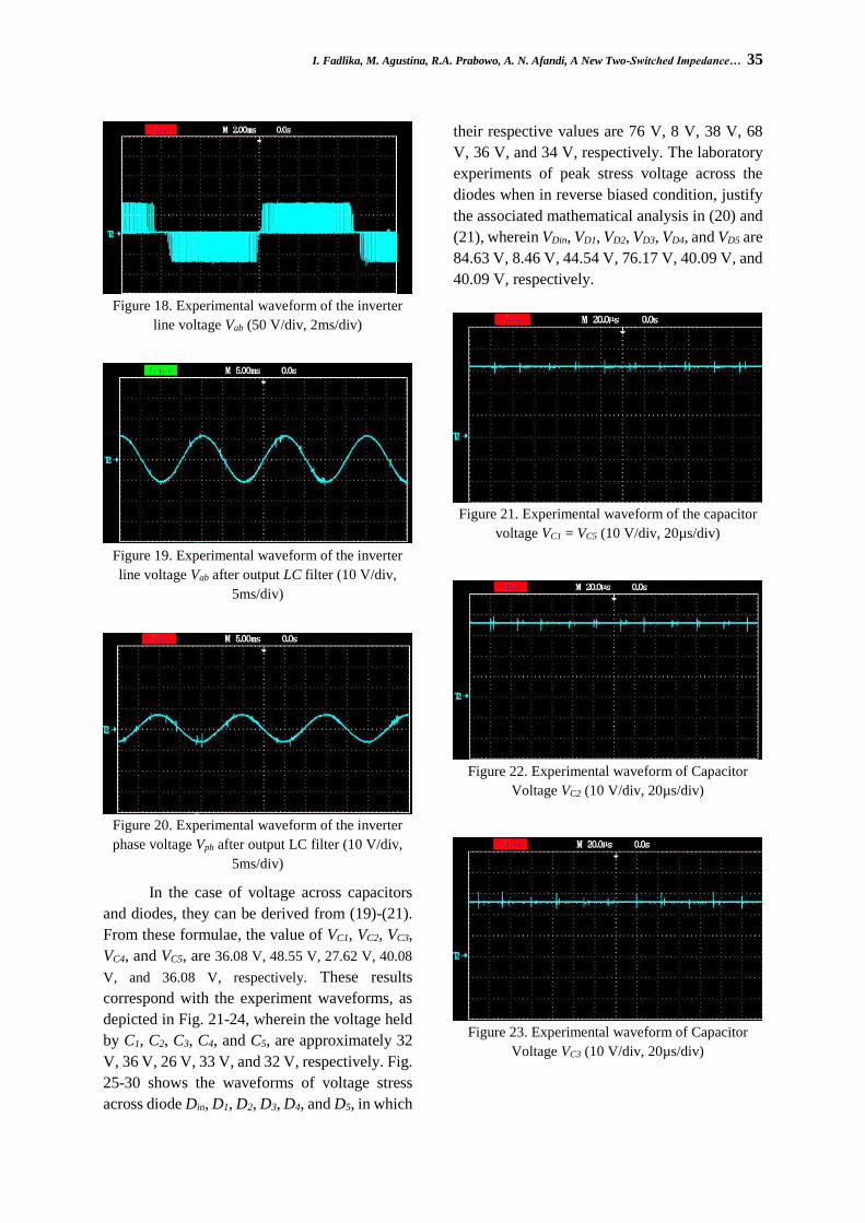
Figure 18. Experimental waveform of the inverter
line voltage Vab (50 V/div, 2ms/div)
Figure 19. Experimental waveform of the inverter
line voltage Vab after output LC filter (10 V/div,
5ms/div)
Figure 20. Experimental waveform of the inverter
phase voltage Vph after output LC filter (10 V/div,
5ms/div)
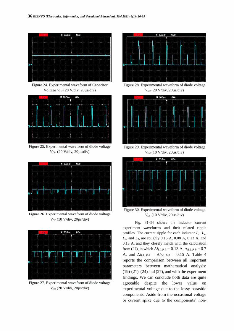
In the case of voltage across capacitors
and diodes, they can be derived from (19)-(21).
From these formulae, the value of VC1, VC2, VC3,
VC4, and VC5, are 36.08 V, 48.55 V, 27.62 V, 40.08
V, and 36.08 V, respectively. These results
correspond with the experiment waveforms, as
depicted in Fig. 21-24, wherein the voltage held
by C1, C2, C3, C4, and C5, are approximately 32
V, 36 V, 26 V, 33 V, and 32 V, respectively. Fig.
25-30 shows the waveforms of voltage stress
across diode Din, D1, D2, D3, D4, and D5, in which
their respective values are 76 V, 8 V, 38 V, 68
V, 36 V, and 34 V, respectively. The laboratory
experiments of peak stress voltage across the
diodes when in reverse biased condition, justify
the associated mathematical analysis in (20) and
(21), wherein VDin, VD1, VD2, VD3, VD4, and VD5 are
84.63 V, 8.46 V, 44.54 V, 76.17 V, 40.09 V, and
40.09 V, respectively.
Figure 21. Experimental waveform of the capacitor
voltage VC1 = VC5 (10 V/div, 20µs/div)
Figure 22. Experimental waveform of Capacitor
Voltage VC2 (10 V/div, 20µs/div)
Figure 23. Experimental waveform of Capacitor
Voltage VC3 (10 V/div, 20µs/div)
36 ELINVO (Electronics, Informatics, and Vocational Education), Mei 2021; 6(1): 26-39
Figure 24. Experimental waveform of Capacitor
Voltage VC4 (20 V/div, 20µs/div)
Figure 25. Experimental waveform of diode voltage
VDin (20 V/div, 20µs/div)
Figure 26. Experimental waveform of diode voltage
VD1 (10 V/div, 20µs/div)
Figure 27. Experimental waveform of diode voltage
VD2 (20 V/div, 20µs/div)
Figure 28. Experimental waveform of diode voltage
VD3 (20 V/div, 20µs/div)
Figure 29. Experimental waveform of diode voltage
VD4 (10 V/div, 20µs/div)
Figure 30. Experimental waveform of diode voltage
VD5 (10 V/div, 20µs/div)
Fig. 31-34 shows the inductor current
experiment waveforms and their related ripple
profiles. The current ripple for each inductor L1, L2,
L3, and L4, are roughly 0.15 A, 0.08 A, 0.13 A, and
0.13 A, and they closely match with the calculation
from (27), in which ∆iL1, P-P = 0.13 A, ∆iL2, P-P = 0.7
A, and ∆iL3, P-P = ∆iL4, P-P = 0.15 A. Table 4
reports the comparison between all important
parameters between mathematical analysis:
(19)-(21), (24) and (27), and with the experiment
findings. We can conclude both data are quite
agreeable despite the lower value on
experimental voltage due to the lossy parasitic
components. Aside from the occasional voltage
or current spike due to the components’ non-
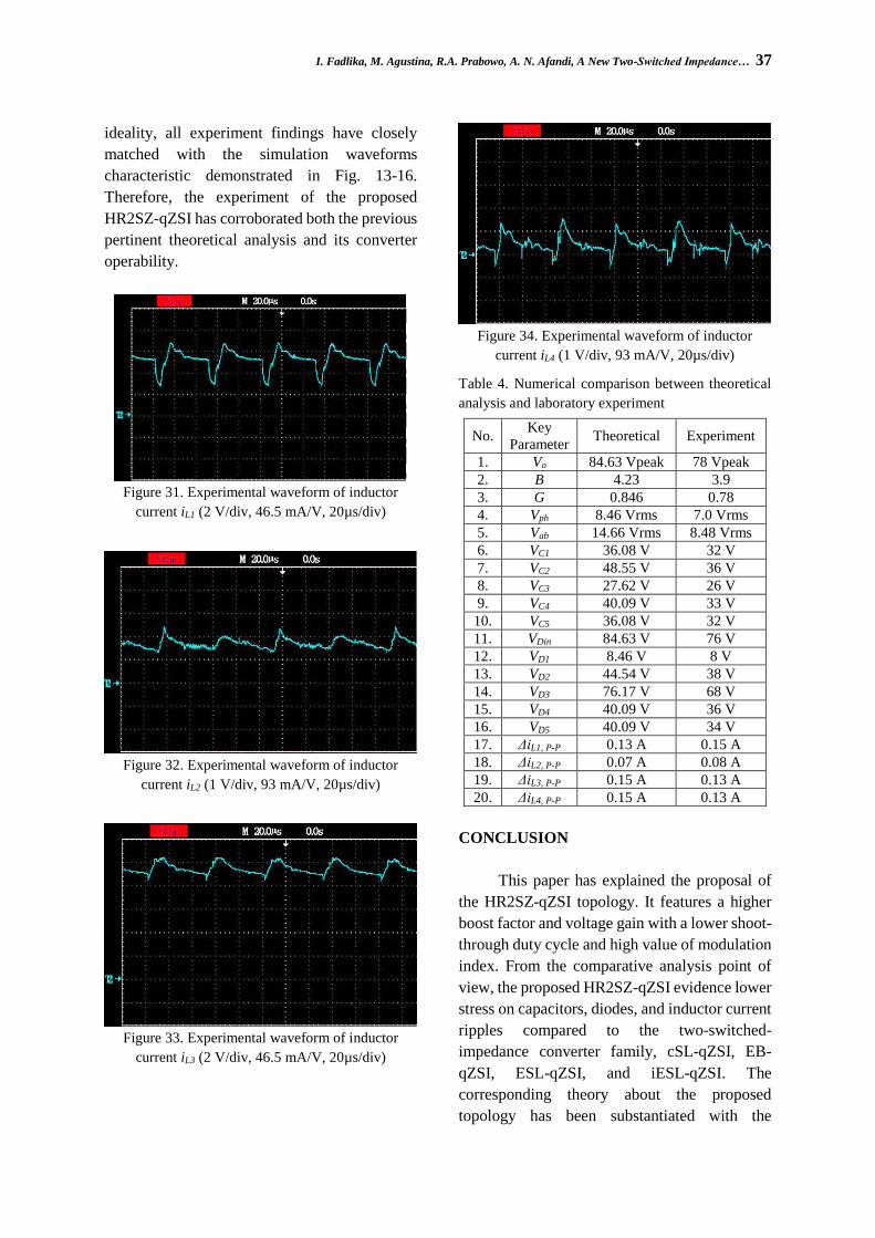
I. Fadlika, M. Agustina, R.A. Prabowo, A. N. Afandi, A New Two-Switched Impedance… 37
ideality, all experiment findings have closely
matched with the simulation waveforms
characteristic demonstrated in Fig. 13-16.
Therefore, the experiment of the proposed
HR2SZ-qZSI has corroborated both the previous
pertinent theoretical analysis and its converter
operability.
Figure 31. Experimental waveform of inductor
current iL1 (2 V/div, 46.5 mA/V, 20µs/div)
Figure 32. Experimental waveform of inductor
current iL2 (1 V/div, 93 mA/V, 20µs/div)
Figure 33. Experimental waveform of inductor
current iL3 (2 V/div, 46.5 mA/V, 20µs/div)
Figure 34. Experimental waveform of inductor
current iL4 (1 V/div, 93 mA/V, 20µs/div)
Table 4. Numerical comparison between theoretical
analysis and laboratory experiment
No. Key
Parameter Theoretical Experiment
1. Vo 84.63 Vpeak 78 Vpeak
2. B 4.23 3.9
3. G 0.846 0.78
4. Vph 8.46 Vrms 7.0 Vrms
5. Vab 14.66 Vrms 8.48 Vrms
6. VC1 36.08 V 32 V
7. VC2 48.55 V 36 V
8. VC3 27.62 V 26 V
9. VC4 40.09 V 33 V
10. VC5 36.08 V 32 V
11. VDin 84.63 V 76 V
12. VD1 8.46 V 8 V
13. VD2 44.54 V 38 V
14. VD3 76.17 V 68 V
15. VD4 40.09 V 36 V
16. VD5 40.09 V 34 V
17. ΔiL1, P-P 0.13 A 0.15 A
18. ΔiL2, P-P 0.07 A 0.08 A
19. ΔiL3, P-P 0.15 A 0.13 A
20. ΔiL4, P-P 0.15 A 0.13 A
CONCLUSION
This paper has explained the proposal of
the HR2SZ-qZSI topology. It features a higher
boost factor and voltage gain with a lower shoot-
through duty cycle and high value of modulation
index. From the comparative analysis point of
view, the proposed HR2SZ-qZSI evidence lower
stress on capacitors, diodes, and inductor current
ripples compared to the two-switched-
impedance converter family, cSL-qZSI, EB-
qZSI, ESL-qZSI, and iESL-qZSI. The
corresponding theory about the proposed
topology has been substantiated with the

38 ELINVO (Electronics, Informatics, and Vocational Education), Mei 2021; 6(1): 26-39
computer simulation and downscale laboratory
experiment. The experiments with dc input
voltage of 20 V, 0.1 ST duty cycle, and 0.2
modulation index have proved the proposed
converter operation along with the respective
important calculated parameters. Interestingly,
this proposed converter preserves the inherent
features of the conventional qZSI: common
ground point between the dc source and
converter and smooth input current operation,
hence it clearly a suitable inverter choice for
renewable energy venture.
ACKNOWLEDGEMENT
We greatly appreciate the State University of
Malang for funding this research work through
the PNBP Research Grant Scheme.
REFERENCES
[1] Erdiwansyah, R. Mamat, M. S. M. Sani, and
K. Sudhakar, “Renewable energy in
Southeast Asia: Policies and
recommendations,” Sci. Total Environ., vol.
670, pp. 1095–1102, 2019, doi:
10.1016/j.scitotenv.2019.03.273.
[2] X. Xu, Z. Wei, Q. Ji, C. Wang, and G. Gao,
“Global renewable energy development:
Influencing factors, trend predictions and
countermeasures,” Resour. Policy, vol. 63,
no. April, 2019, doi:
10.1016/j.resourpol.2019.101470.
[3] A. K. Shukla, K. Sudhakar, and P. Baredar,
“Renewable energy resources in South Asian
countries: Challenges, policy and
recommendations,” Resour. Technol., vol. 3,
no. 3, pp. 342–346, 2017, doi:
10.1016/j.reffit.2016.12.003.
[4] M. M. Vanegas Cantarero, “Of renewable
energy, energy democracy, and sustainable
development: A roadmap to accelerate the
energy transition in developing countries,”
Energy Res. Soc. Sci., vol. 70, no. July, p.
101716, 2020, doi:
10.1016/j.erss.2020.101716.
[5] IRENA, “World Energy Transitions Outlook:
1.5°C Pathway,” 2021. [Online]. Available:
https://irena.org/publications/2021/March/W
orld-Energy-Transitions-Outlook.
[6] A. Kalair, N. Abas, M. S. Saleem, A. R.
Kalair, and N. Khan, “Role of energy storage
systems in energy transition from fossil fuels
to renewables,” Energy Storage, vol. 3, no. 1,
pp. 1–27, 2021, doi: 10.1002/est2.135.
[7] K. Hansen, C. Breyer, and H. Lund, “Status
and perspectives on 100% renewable energy
systems,” Energy, vol. 175, pp. 471–480,
2019, doi: 10.1016/j.energy.2019.03.092.
[8] H. Nugroho, S. Fei-Lu, and Firmansyah,
“Developing renewable energy in developing
countries: A lesson from Indonesia,” Energy
Sources, Part B Econ. Plan. Policy, vol. 12,
no. 4, pp. 318–325, 2017, doi:
10.1080/15567249.2015.1072599.
[9] S. Kusch-Brandt, “Urban Renewable Energy
on the Upswing: A Spotlight on Renewable
Energy in Cities in REN21’s ‘Renewables
2019 Global Status Report,’” Resources, vol.
8, no. 3, p. 139, 2019, doi:
10.3390/resources8030139.
[10] IRENA, “Renewable capacity statistics
2021,” 2021. [Online]. Available:
https://www.irena.org/publications/2021/Ma
rch/Renewable-Capacity-Statistics-2021.
[11] REN21, “Ren21,” 2020. [Online]. Available:
https://www.ren21.net/wp-
content/uploads/2019/05/gsr_2020_full_repo
rt_en.pdf.
[12] F. Blaabjerg, Z. Chen, and S. B. Kjaer,
“Power electronics as efficient interface in
dispersed power generation systems,” IEEE
Trans. Power Electron., vol. 19, no. 5, pp.
1184–1194, 2004, doi:
10.1109/TPEL.2004.833453.
[13] R. Panigrahi, S. K. Mishra, S. C. Srivastava,
A. K. Srivastava, and N. N. Schulz, “Grid
Integration of Small-Scale Photovoltaic
Systems in Secondary Distribution Network -
A Review,” IEEE Trans. Ind. Appl., vol. 56,
no. 3, pp. 3178–3195, 2020, doi:
10.1109/TIA.2020.2979789.
[14] Z. A. Arfeen, A. B. Khairuddin, R. M. Larik,
and M. S. Saeed, “Control of distributed
generation systems for microgrid
applications: A technological review,” Int.
Trans. Electr. Energy Syst., vol. 29, no. 9, pp.
1–26, 2019, doi: 10.1002/2050-7038.12072.
[15] Q. Li and P. Wolfs, “A Review of the Single
Phase Photovoltaic Module Integrated
Converter Topologies With Three Different
DC Link Configuration,” IEEE Trans. Power
Electron., vol. 23, no. 3, pp. 1320–1333,
2008, doi: 10.1109/TPEL.2008.920883.
[16] S. B. Kjaer, J. K. Pedersen, and F. Blaabjerg,
“A Review of Single-Phase Grid-Connected
Inverters for Photovoltaic Modules,” IEEE
Trans. Ind. Appl., vol. 41, no. 5, pp. 1292–
1306, 2005, doi: 10.1109/TIA.2005.853371.

I. Fadlika, M. Agustina, R.A. Prabowo, A. N. Afandi, A New Two-Switched Impedance… 39
[17] A. M. Prasetia and H. Santoso,
“Implementation of Scalar Control Method
for 3 Phase Induction Motor Speed Control,”
Elinvo (Electronics, Informatics, Vocat.
Educ., vol. 3, no. 1, pp. 63–69, 2018, doi:
10.21831/elinvo.v3i1.19460.
[18] F. Z. Peng, “Z-Source Inverter,” IEEE Trans.
Ind. Appl., vol. 39, no. 2, pp. 504–510, 2003,
doi: 10.1109/TIA.2003.808920.
[19] J. Anderson and F. Z. Peng, “Four quasi-Z-
Source inverters,” in IEEE Power Electronics
Specialists Conference, 2008, pp. 2743–
2749, doi: 10.1109/PESC.2008.4592360.
[20] Y. Liu, H. Abu-Rub, and B. Ge, “Z-
source/quasi-Z-source inverters: Derived
networks, modulations, controls, and
emerging applications to photovoltaic
conversion,” IEEE Industrial Electronics
Magazine, vol. 8, no. 4, pp. 32–44, 2014.
[21] Y. Liu, B. Ge, H. Abu-Rub, and H. Sun,
“Hybrid Pulsewidth Modulated Single-Phase
Quasi-Z-Source Grid-Tie Photovoltaic Power
System,” IEEE Trans. Ind. Informatics, vol.
12, no. 2, pp. 621–632, 2016, doi:
10.1109/TII.2016.2524561.
[22] M. Meraj, S. Rahman, A. Iqbal, and L. Ben-
Brahim, “Common Mode Voltage Reduction
in a Single-Phase Quasi Z-Source Inverter for
Transformerless Grid-Connected Solar PV
Applications,” IEEE J. Emerg. Sel. Top.
Power Electron., vol. 7, no. 2, pp. 1352–
1363, 2019, doi:
10.1109/JESTPE.2018.2867521.
[23] Y. Liu, B. Ge, H. Abu-Rub, and D. Sun,
“Comprehensive Modeling of Single-Phase
Quasi-Z-Source Photovoltaic Inverter to
Investigate Low-Frequency Voltage and
Current Ripple,” IEEE Trans. Ind. Electron.,
vol. 62, no. 7, pp. 4194–4202, 2015, doi:
10.1109/TIE.2014.2384472.
[24] Y. Liu, B. Ge, H. Abu-Rub, and F. Z. Peng,
“Control System Design of Battery-Assisted
Quasi-Z-Source Inverter for Grid-Tie
Photovoltaic Power Generation,” IEEE
Trans. Sustain. Energy, vol. 4, no. 4, pp. 994–
1001, 2013, doi:
10.1109/TSTE.2013.2263202.
[25] Y. Li, S. Jiang, J. G. Cintron-Rivera, and F.
Z. Peng, “Modeling and control of quasi-z-
source inverter for distributed generation
applications,” IEEE Trans. Ind. Electron.,
vol. 60, no. 4, pp. 1532–1541, 2013, doi:
10.1109/TIE.2012.2213551.
[26] B. Ge et al., “An energy-stored quasi-Z-
source inverter for application to photovoltaic
power system,” IEEE Trans. Ind. Electron.,
vol. 60, no. 10, pp. 4468–4481, 2013, doi:
10.1109/TIE.2012.2217711.
[27] H. Abu-Rub, A. Iqbal, S. M. Ahmed, F. Z.
Peng, Y. Li, and G. Baoming, “Quasi-Z-
source inverter-based photovoltaic
generation system with maximum power
tracking control using ANFIS,” IEEE Trans.
Sustain. Energy, vol. 4, no. 1, pp. 11–20,
2013, doi: 10.1109/TSTE.2012.2196059.
[28] M. Zhu, K. Yu, and F. L. Luo, “Switched
Inductor Z-Source Inverter,” IEEE Trans.
POWER Electron., vol. 25, no. 8, pp. 2150–
2158, 2010, doi:
10.1109/TPEL.2010.2046676.
[29] M.-K. Nguyen, Y.-C. Lim, and G.-B. Cho,
“Switched-Inductor Quasi-Z-Source
Inverter,” IEEE Trans. Power Electron., vol.
26, no. 11, pp. 3183–3191, 2011, doi:
10.1109/TIE.2017.2688964.
[30] M. K. Nguyen, Y. C. Lim, and J. H. Choi,
“Two switched-inductor quasi-Z-source
inverters,” IET Power Electron., vol. 5, no. 7,
pp. 1017–1025, 2012, doi: 10.1049/iet-
pel.2011.0297.
[31] V. Jagan, J. Kotturu, and S. Das, “Enhanced-
Boost Quasi-Z-Source Inverters with Two-
Switched Impedance Networks,” IEEE
Trans. Ind. Electron., vol. 64, no. 9, pp.
6885–6897, 2017, doi:
10.1109/TIE.2017.2688964.
[32] M. Abbasi, A. H. Eslahchi, and M. Mardaneh,
“Two Symmetric Extended-Boost Embedded
Switched-Inductor Quasi-Z-Source Inverter
with Reduced Ripple Continuous Input
Current,” IEEE Trans. Ind. Electron., vol. 65,
no. 6, pp. 5096–5104, 2018, doi:
10.1109/TIE.2017.2779433.


![A FAST DIRECT SOLVER FOR QUASI-PERIODIC SCATTERING … · to use the quasi-periodic impedance half-space Green’s function [32, 3]. However, all such periodized kernel methods do](https://img.dokumen.tips/doc/110x75/5e2f1d0348871514623e9ac5/a-fast-direct-solver-for-quasi-periodic-scattering-to-use-the-quasi-periodic-impedance.jpg)


![Enhanced-Boost Quasi-Z-Source Inverters with Two Switched … · 2017-09-26 · switched inductor (SL) cells and are proposed in [7] and [8] Enhanced-Boost Quasi-Z-Source Inverters](https://img.dokumen.tips/doc/110x75/5f0a34397e708231d42a83cb/enhanced-boost-quasi-z-source-inverters-with-two-switched-2017-09-26-switched.jpg)
![Single Switched Capacitor High Gain Boost Quasi-Z Source Converter · 2018-08-16 · 1[17], and the quasi-Z-Source converter in Fig -2 [32], the proposed converter is depicted in](https://img.dokumen.tips/doc/110x75/5f4d972568593756d475e483/single-switched-capacitor-high-gain-boost-quasi-z-source-converter-2018-08-16.jpg)