Embed Size (px)
Citation preview

The University of Mississippi Department of Electrical EngineeringC
ente
r of
App
lied
Ele
ctro
mag
netic
Sys
tem
s Res
earc
h (C
AE
SR)
http://www.ee.olemiss.edu
Metamaterial Surfaces: A New Paradigm in Electromagnetics
Prof. Fan YangDepartment of Electrical Engineering, University of Mississippi

The University of Mississippi Department of Electrical EngineeringC
ente
r of
App
lied
Ele
ctro
mag
netic
Sys
tem
s Res
earc
h (C
AE
SR)
http://www.ee.olemiss.edu
OUTLINEOverview of metamaterial surfaces
Characterizations and designs
Various EM applications
A simple and efficient FDTD/PBC algorithm
Basic idea: constant kx method
Numerical examples
A low profile surface wave antenna
Antenna concept
Designs and verifications
Conclusions

The University of Mississippi Department of Electrical EngineeringC
ente
r of
App
lied
Ele
ctro
mag
netic
Sys
tem
s Res
earc
h (C
AE
SR)
http://www.ee.olemiss.edu
Meta-Materials
Meta: a prefix means “beyond”Meta-materials: engineered materials with superior electromagnetic properties
Double negative (DNG) materials
Left handed materials
Magneto-materials
Electromagnetic band-gap (EBG) structures
Artificial magnetic conductor
Volumetric structure (3D) and Planar structure (2D)

The University of Mississippi Department of Electrical EngineeringC
ente
r of
App
lied
Ele
ctro
mag
netic
Sys
tem
s Res
earc
h (C
AE
SR)
http://www.ee.olemiss.edu
Meta-material Surfaces
Meta-material surfaces such as frequency selective surfaces (FSS), soft and hard surfaces, and electromagnetic band gap structures have unique EM properties due to the inherent periodicity.
Electromagnetic band gap structures have been presented recently and extensive research has been conducted in this topic.
It exhibits a stop band for surface wavesand an in-phase reflection coefficient.
The meta-material surfaces have been widely used in various EM applications to improve the performance of RF devices.Mushroom-like EBG surface
Top view
Cross view
C
L

The University of Mississippi Department of Electrical EngineeringC
ente
r of
App
lied
Ele
ctro
mag
netic
Sys
tem
s Res
earc
h (C
AE
SR)
http://www.ee.olemiss.edu
Introduction of EBG Ground Plane
EBG ground plane:
PEC ground
Dielectric substrate
Periodic patches
Connecting vias
y
x Top View
x
z
Cross View
Geometry of an EBG ground plane
W=0.12 λ
g=0.02 λ
h=0.04 λ
εr=2.20
EBG ground planes can be easily fabricated by the PCB (Printed Circuit Board) technique.
They are analyzed using the finite different time domain (FDTD) method.

The University of Mississippi Department of Electrical EngineeringC
ente
r of
App
lied
Ele
ctro
mag
netic
Sys
tem
s Res
earc
h (C
AE
SR)
http://www.ee.olemiss.edu
Band Gap for Surface Wave Suppression
0.0 4.0 8.0 12.00.0
4.0
8.0
12.0
X (cm)Y
(cm
)
-20.0 0.0 20.0 40.0 60.0
20*log|E| (dB)
40
30
20
0.0 4.0 8.0 12.00.0
4.0
8.0
12.0
X (cm)
Y (
cm)
-20.0 0.0 20.0 40.0 60.0
20*log|E| (dB)
40
30
2010
EBG case PEC case

The University of Mississippi Department of Electrical EngineeringC
ente
r of
App
lied
Ele
ctro
mag
netic
Sys
tem
s Res
earc
h (C
AE
SR)
http://www.ee.olemiss.edu
In-Phase Reflection for Plane Wave Incidence
PML
PBC
Plane wave incidence
Observational plane
0 5 10 15 20 25−200
−150
−100
−50
0
50
100
150
200
Freq (GHz)
Ref
lect
ion
phas
e (D
egre
e)
FDTDRef.PEC
PMCEBG
Reflection phase results
Observation: The phase of the reflection coefficient of an EBG structure changes from 180˚ to -180˚ with frequency, while it is 180˚for a PEC and 0˚ for a PMC surface. The simulated result agrees well with the data in a reference paper.

The University of Mississippi Department of Electrical EngineeringC
ente
r of
App
lied
Ele
ctro
mag
netic
Sys
tem
s Res
earc
h (C
AE
SR)
http://www.ee.olemiss.edu
Polarization Dependent EBG Surface Designs
Top view
Cross view
Top view
Cross view
Top view
Cross view
Square patch EBGIndependent of polarization
Top view
Cross view
Offset viasRectangular EBG
Slot loaded EBG

The University of Mississippi Department of Electrical EngineeringC
ente
r of
App
lied
Ele
ctro
mag
netic
Sys
tem
s Res
earc
h (C
AE
SR)
http://www.ee.olemiss.edu
Rectangular Patch EBG Surface
Remarks:
1. Rectangular patch dimensions: W=0.16λ3GHz, L=0.24λ3GHz.
2. The reflection phase is dependent on the wave polarization.
3. Z polarization: θ=90˚, f=3.07 GHz; θ=-90˚, f=4.09 GHz.
4. Y polarization: θ=90˚, f=2.41 GHz; θ=-90˚, f=2.99 GHz.
Top view
Cross view2 2.5 3 3.5 4 4.5
−200
−150
−100
−50
0
50
100
150
200
Freq (GHz)
Ref
lect
ion
phas
e (D
egre
e)
Z polY pol
y
z

The University of Mississippi Department of Electrical EngineeringC
ente
r of
App
lied
Ele
ctro
mag
netic
Sys
tem
s Res
earc
h (C
AE
SR)
http://www.ee.olemiss.edu
Slot Loaded Patch EBG Surface
Top view
Cross view
Remarks:
1. Square patch with slots: Ws=0.02λ3GHz, L=0.12λ3GHz, Ps=0.04λ3GHz.
2. The reflection phase is dependent on the wave polarizations.
3. Z polarization: θ =90˚, f=3.07 GHz; θ=-90˚, f=4.08 GHz.
4. Y polarization: θ=90˚, f=2.87 GHz; θ=-90˚, f=3.51 GHz.
y
z
2 2.5 3 3.5 4 4.5−200
−150
−100
−50
0
50
100
150
200
Freq (GHz)
Ref
lect
ion
phas
e (D
egre
e)
No slot Slot, Z polSlot, Y pol

The University of Mississippi Department of Electrical EngineeringC
ente
r of
App
lied
Ele
ctro
mag
netic
Sys
tem
s Res
earc
h (C
AE
SR)
http://www.ee.olemiss.edu
Square Patch with Offset Vias
2 2.5 3 3.5 4 4.5−200
−150
−100
−50
0
50
100
150
200
Freq (GHz)
Ref
lect
ion
phas
e (D
egre
e)
Via at 1/2 WVia at 3/8 WVia at 1/4 WVia at 0 Top view
Cross view
y
z
Remarks:
1. The vias move along the Y direction: 1/2 W, 3/8 W, 1/4 W, 0.
2. The reflection phase of Y polarized waves changes with vias’position while it remains the same for Z polarized waves.
3. Dual resonance is observed for Y polarized plane wave.

The University of Mississippi Department of Electrical EngineeringC
ente
r of
App
lied
Ele
ctro
mag
netic
Sys
tem
s Res
earc
h (C
AE
SR)
http://www.ee.olemiss.edu
With or Without Vias ?
Mushroom EBG ground planeWITH VIAS
y
x Top View
x
z
Cross View
y
x Top View
x
z
Cross ViewPatch loaded grounded slab
NO VIAS
W=0.10 λ
g=0.02 λ
h=0.04 λ
εr=2.94
λ=75 mm
r =0.005 λ

The University of Mississippi Department of Electrical EngineeringC
ente
r of
App
lied
Ele
ctro
mag
netic
Sys
tem
s Res
earc
h (C
AE
SR)
http://www.ee.olemiss.edu
Surface Wave Property
X M0
1
2
3
4
5
6
7
8
9
10
Fre
quen
cy (
GH
z)
Γ Γ
Band Gap
Light line Light line
First mode
Second mode
Wavenumber X M
0
1
2
3
4
5
6
7
8
9
10
Fre
quen
cy (
GH
z)
Γ Γ
No Band Gap
Light line Light line
First mode
Second mode
Wavenumber
No Band GapBand Gap
With vias No viasRemarks:1. The dispersion diagrams of both artificial complex ground planes
have been determined using the spectral FDTD method.2. When the vias in the mushroom structure is removed, the band gap
disappears. For the patch loaded grounded slab, the TM surface wave (the first mode) exists at all frequencies.

The University of Mississippi Department of Electrical EngineeringC
ente
r of
App
lied
Ele
ctro
mag
netic
Sys
tem
s Res
earc
h (C
AE
SR)
http://www.ee.olemiss.edu
Plane Wave Property
0 2 4 6 8 10 12−200
−150
−100
−50
0
50
100
150
200
Freq. (GHz)
Ref
lect
ion
phas
e (D
egre
e)
With viasNo vias
PML
PBC
Plane wave incidence
Observational plane
Reflection coefficients for normal incidence
Remarks: Reflection phases of both ground planes are almost identical to each other for normal incidence.

The University of Mississippi Department of Electrical EngineeringC
ente
r of
App
lied
Ele
ctro
mag
netic
Sys
tem
s Res
earc
h (C
AE
SR)
http://www.ee.olemiss.edu
OUTLINEOverview of metamaterial surfaces
Characterizations and designs
Various EM applications
A simple and efficient FDTD/PBC algorithm
Basic idea: constant kx method
Numerical examples
A low profile surface wave antenna
Antenna concept
Designs and verifications
Conclusions

The University of Mississippi Department of Electrical EngineeringC
ente
r of
App
lied
Ele
ctro
mag
netic
Sys
tem
s Res
earc
h (C
AE
SR)
http://www.ee.olemiss.edu
EBG Application in Microstrip Patch Antenna
−150 −100 −50 0 50 100 150−30
−25
−20
−15
−10
−5
0
Angle (Degree)
Pat
tern
(dB
)
EBG
Thick Sub.
Step−Like
Thin Sub.
A patch antennasurrounded by EBG structures E plane patternsRemarks:1. A compact microstrip antenna on a high dielectric constant substrate
usually suffers from severe surface waves2. The EBG structure can effectively suppress the surface waves,
resulting in a high antenna gain and low back radiation.

The University of Mississippi Department of Electrical EngineeringC
ente
r of
App
lied
Ele
ctro
mag
netic
Sys
tem
s Res
earc
h (C
AE
SR)
http://www.ee.olemiss.edu
EBG Application in Microstrip Patch Array
5.2 5.4 5.6 5.8 6 6.2 6.4−30
−25
−20
−15
−10
−5
0
Remarks: 1. Mutual coupling in phased antenna arrays needs to be reduced in order
to enhance the performance of the radar systems.2. When the EBG structure is inserted between antennas, the mutual
coupling is reduced from -16.8 dB to -24.6 dB.
Freq (GHz)
S (
dB)
No EBG With EBG
S11
S12

The University of Mississippi Department of Electrical EngineeringC
ente
r of
App
lied
Ele
ctro
mag
netic
Sys
tem
s Res
earc
h (C
AE
SR)
http://www.ee.olemiss.edu
Low Profile High Efficiency Antenna Designs
Options Efficiency Low Profile Antennas
PECJ
PECJ
PMCJ
Monopole
N/A
Microstrip
New frontier
M
PEC
Goal: Goal: To develop low profile and high efficiency antennas on PMC-like ground planes.

The University of Mississippi Department of Electrical EngineeringC
ente
r of
App
lied
Ele
ctro
mag
netic
Sys
tem
s Res
earc
h (C
AE
SR)
http://www.ee.olemiss.edu
Wire Antennas On Meta-Material Surfaces
Wire antennas, such as dipole, loop, curl, ...
Full wave numerical analysis tools, such as FDTD, MoM, …
Innovative antenna designs with versatile functionality for wireless communications
Artificial complex ground planes, such as EBG, soft/hard surfaces, FSS, ...
The University of Mississippi Department of Electrical EngineeringC
ente
r of
App
lied
Ele
ctro
mag
netic
Sys
tem
s Res
earc
h (C
AE
SR)
http://www.ee.olemiss.edu
Curl Antennas for Wireless Communication
Curl antenna features: Curl antenna features:
1. Simple structure.
2. Circularly polarized pattern.
Curl Antenna
PEC ground plane
Curl antennas on a PEC ground planeCurl antennas on a PEC ground plane::
When a curl antenna is positioned above a PEC ground plane, a relative large height (0.20 λ) is required to good CP pattern.
Research goal: Research goal: To design a low profile curl antenna with good CP pattern suitable for GPS, WLAN, and other wireless communications.

The University of Mississippi Department of Electrical EngineeringC
ente
r of
App
lied
Ele
ctro
mag
netic
Sys
tem
s Res
earc
h (C
AE
SR)
http://www.ee.olemiss.edu
Curl on EBG Ground: Experiment Results
52 mm
13 mm
4 5 6 7 8 9 10−20
−15
−10
−5
0
Freq (GHz)
S11
(dB
)
EBGPEC
Remarks:Remarks:1. An EBG ground plane is fabricated on a RT/duroid 5880 (εr=2.20, h=2 mm) substrate. The EBG patch width is 6 mm and gap width is 1 mm.2. The parameters of the curl are: R=5.5 mm, L=5 mm, h=3mm.3. The curl antenna exhibits a good return loss with the low profile configuration.

The University of Mississippi Department of Electrical EngineeringC
ente
r of
App
lied
Ele
ctro
mag
netic
Sys
tem
s Res
earc
h (C
AE
SR)
http://www.ee.olemiss.edu
Dipole Antenna on PDEBG: Circular Polarization
BASIC IDEASBASIC IDEAS
Low Profile:
PEC:
PMC:
Artificial ground:
0→kd
0, === Eyx
rπθθ
LINEAR polarization.
2,
2πθπθ −== yx
CIRCULAR polarization!
Dipole
PDEBG surface
Dipole
Ground plane
x
y
)ˆˆ(21
)ˆˆ(21
22 yx jkdjjkzjkdjjkz
jkzjkz
eyex
eyexE
θθ +−−+−−
−−
⋅+⋅+
⋅+⋅=r
jkzjkzyx ezexE −− ⋅+⋅=== ˆˆ,0
rθθ
)]ˆˆ()ˆˆ[(21 yxjyxeE jkz −⋅++= −
r
Direct
Reflected

The University of Mississippi Department of Electrical EngineeringC
ente
r of
App
lied
Ele
ctro
mag
netic
Sys
tem
s Res
earc
h (C
AE
SR)
http://www.ee.olemiss.edu
Dipole on EBG Ground: Experiment Results (1)
75 mm
34 mm
Remarks:Remarks:1. An PDEBG ground plane is fabricated on a RT/duroid 6002 (εr=2.94, h=6 mm) substrate. Rectangular EBG patches are used with 13 mm length and 8 mm width. The gap width is 2 mm.2. A dipole (L=34 mm, h=3 mm) is oriented along 45˚ direction.3. The antenna exhibits a good return loss (S11<-10 dB) from 3.25-4.14 GHz.
1 2 3 4 5−20
−15
−10
−5
0
Freq. (GHz)
S11
(dB
)

The University of Mississippi Department of Electrical EngineeringC
ente
r of
App
lied
Ele
ctro
mag
netic
Sys
tem
s Res
earc
h (C
AE
SR)
http://www.ee.olemiss.edu
Dipole on EBG Ground: Experiment Results (2)
1 2 3 4 50
2
4
6
8
10
Freq (GHz)
AR
(dB
)
−50 0 500
2
4
6
8
10
θ (Degree)
AR
(dB
)
xzyz
Axial ratio vs. frequency Axial ratio vs. θ
Remarks:Remarks:1. A good axial ratio of 2 dB is obtained at 3.56 GHz and the bandwidth (AR <3dB) is 5.6%.2. The axial ratio vs. elevation angle is measured at 3.56 GHz and the beamwidth (AR <3dB) is around 30˚.

The University of Mississippi Department of Electrical EngineeringC
ente
r of
App
lied
Ele
ctro
mag
netic
Sys
tem
s Res
earc
h (C
AE
SR)
http://www.ee.olemiss.edu
Reconfigurable Antennas with Switching Beams (1)
Single bent monopole
Feed x
y
z
1-D beam switch
Feedx
y
z
1 2
12
2-D beam switch
Feedx
y
z
1 2
3
4
1 23 4
Remarks:1. Reconfigurable radiation pattern is challenging for an antenna elementelement .
2. A bent monopole on EBG ground plane radiates a tilted antenna beam.
3. This property is utilized to construct reconfigurable antennas with 1-D or 2-D switching beams.

The University of Mississippi Department of Electrical EngineeringC
ente
r of
App
lied
Ele
ctro
mag
netic
Sys
tem
s Res
earc
h (C
AE
SR)
http://www.ee.olemiss.edu
Reconfigurable Antennas with Switching Beams (2)
−15 dB
−10 dB
−5 dB
0 dB 30°
−150°
60°
−120°
90°−90°
120°
−60°
150°
−30°
180°
0°
xz planeEBG
Bent monopole
75 mm
30 mm
Remarks:1. A reconfigurable bent monopole antenna on a EBG ground plane is
designed, fabricated, and tested. The antenna height is 0.02 λ.2. The antenna resonates at 4.32 GHz with 10.6% bandwidth (450
MHz, 4.04-4.49 GHz).3. The antenna beam switches between ±29˚ with a gain of 6.5 dB.

The University of Mississippi Department of Electrical EngineeringC
ente
r of
App
lied
Ele
ctro
mag
netic
Sys
tem
s Res
earc
h (C
AE
SR)
http://www.ee.olemiss.edu
OUTLINEOverview of metamaterial surfaces
Characterizations and designs
Various EM applications
A simple and efficient FDTD/PBC algorithm
Basic idea: constant kx method
Numerical examples
A low profile surface wave antenna
Antenna concept
Designs and verifications
Conclusions

The University of Mississippi Department of Electrical EngineeringC
ente
r of
App
lied
Ele
ctro
mag
netic
Sys
tem
s Res
earc
h (C
AE
SR)
http://www.ee.olemiss.edu
FDTD Analysis of Periodic Structures
Many electromagnetic structures possess a periodicity in one or more directions, such as FSS, EBG, antenna array.
To alleviate the computational burden, one ways is to model only one individual element and use periodic boundary conditions to simulate the effect of periodic replication.

The University of Mississippi Department of Electrical EngineeringC
ente
r of
App
lied
Ele
ctro
mag
netic
Sys
tem
s Res
earc
h (C
AE
SR)
http://www.ee.olemiss.edu
Fundamental Challenge of PBC
)exp(),,(),,0()exp(),,(),,0(ajkzyaxzyxajkzyaxzyx
x
x
======
HHEE
:domain Frequency
PML
PML
PBC
Periodic structure
Ckkx /sinsin0 θωθ =⋅=
z
)/sin,,(),,,0()/sin,,(),,,0(CatyaxEtzyxECatyaxEtzyxE
θθ
+===+===
:domain Time
x
Fundamental challenge: Data at future time are needed.
The University of Mississippi Department of Electrical EngineeringC
ente
r of
App
lied
Ele
ctro
mag
netic
Sys
tem
s Res
earc
h (C
AE
SR)
http://www.ee.olemiss.edu
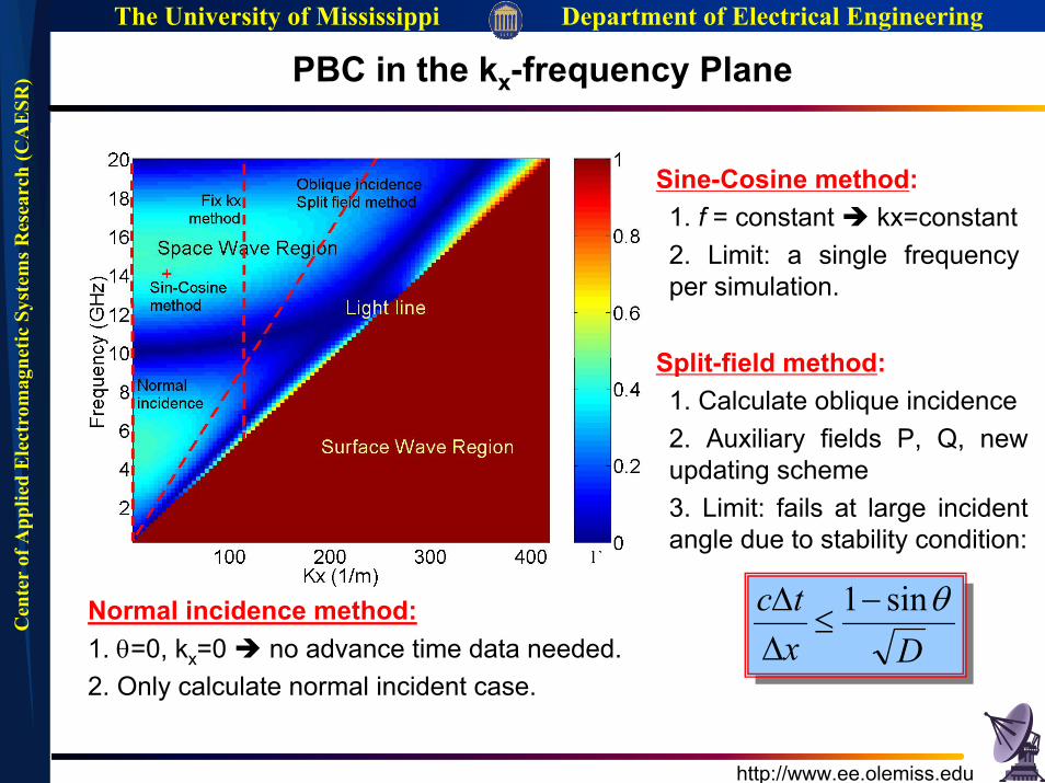
PBC in the kx-frequency Plane
Normal incidence method:1. θ=0, kx=0 no advance time data needed.2. Only calculate normal incident case.
Sine-Cosine method:1. f = constant kx=constant2. Limit: a single frequency per simulation.
Split-field method:1. Calculate oblique incidence2. Auxiliary fields P, Q, new updating scheme3. Limit: fails at large incident angle due to stability condition:
Dxtc θsin1−≤
∆∆

The University of Mississippi Department of Electrical EngineeringC
ente
r of
App
lied
Ele
ctro
mag
netic
Sys
tem
s Res
earc
h (C
AE
SR)
http://www.ee.olemiss.edu
New PBC in FDTD: Constant Kx Method (1)
Ckx /sinθω=
Fix kxmethod
Split field method
)exp(),,,(),,,0(
ajktzyaxEtzyxE
x===
:domain Time
Basic idea: Calculate along a vertical line in the kx-frequency domain.

The University of Mississippi Department of Electrical EngineeringC
ente
r of
App
lied
Ele
ctro
mag
netic
Sys
tem
s Res
earc
h (C
AE
SR)
http://www.ee.olemiss.edu
New PBC in FDTD: Constant Kx Method (2)
PML
PML
PBC
Periodic structure
z
Implementation:Implementation:1. In the main computational domain, standard
Yee’s algorithm2. A simple updating equation in the boundary
Advantages of the constant Advantages of the constant kkxx method:method:1. Simple to implement
Use (E, H) instead of (P, Q)Standard Yee’s updating schemeSame PML
2. Efficient in computationSame stability conditiondt independent of incident angle and kx
)exp(),,,(),,,0( ajktzyaxEtzyxE x===
x

The University of Mississippi Department of Electrical EngineeringC
ente
r of
App
lied
Ele
ctro
mag
netic
Sys
tem
s Res
earc
h (C
AE
SR)
http://www.ee.olemiss.edu
Example: A Dipole FSS (1)
Geometry:Geometry:
1. A dipole frequency selective surface mounted on a dielectric slab.
2. The length of the dipole is 12 mm and the width is 3 mm. The periodicity is 15 mm both along x and y directions.
3. The dielectric slab has a thickness of 6 mm and dielectric constant of 2.2.
4. A TEz plane wave incidents into the structure in the xz plane
Top view
Cross view
x
y
x
z

The University of Mississippi Department of Electrical EngineeringC
ente
r of
App
lied
Ele
ctro
mag
netic
Sys
tem
s Res
earc
h (C
AE
SR)
http://www.ee.olemiss.edu
Example: A Dipole FSS (2)
Surface wave region
Reflection
Transmission
Reflection

The University of Mississippi Department of Electrical EngineeringC
ente
r of
App
lied
Ele
ctro
mag
netic
Sys
tem
s Res
earc
h (C
AE
SR)
http://www.ee.olemiss.edu
Example: A Dipole FSS (3)
Surface wave region
6 8 10 12 14 160
0.1
0.2
0.3
0.4
0.5
0.6
0.7
0.8
0.9
1R
efle
ctio
n co
effic
ient
Frequency (GHz)
θ= 0°, Split−field
θ= 0°, Fix Kx
θ=15°, Split−field
θ=15°, Fix Kx
θ=30°, Split−field
θ=30°, Fix Kx
θ=45°, Split−field
θ=45°, Fix Kx

The University of Mississippi Department of Electrical EngineeringC
ente
r of
App
lied
Ele
ctro
mag
netic
Sys
tem
s Res
earc
h (C
AE
SR)
http://www.ee.olemiss.edu
Geometry of Periodic PEC Patches
1cm
0.5cm
Top view Side view
300
1cm 0.5cm
TE wave
Parameters:1. FDTD grid size: 0.5 mm=0.01λ6GHz. Each element includes 20×20
cells.2. Kx ranges from 0 to 838 (1/m) (~40 GHz).3. TE incidence case, extract the reflection coefficients for 0º, 30º,
60º, 85º.

The University of Mississippi Department of Electrical EngineeringC
ente
r of
App
lied
Ele
ctro
mag
netic
Sys
tem
s Res
earc
h (C
AE
SR)
http://www.ee.olemiss.edu
Reflection Coefficient in kx-frequency plane

The University of Mississippi Department of Electrical EngineeringC
ente
r of
App
lied
Ele
ctro
mag
netic
Sys
tem
s Res
earc
h (C
AE
SR)
http://www.ee.olemiss.edu
Constant kx Method vs. Split Field Method (1)
30º TE caseNormal incidenceRemarks:1. Reflection coefficient vs. angle is extracted from the kx-f plane and
the result is compared with the split field method.2. The results agree with each other for normal and 30º TE incident
cases.

The University of Mississippi Department of Electrical EngineeringC
ente
r of
App
lied
Ele
ctro
mag
netic
Sys
tem
s Res
earc
h (C
AE
SR)
http://www.ee.olemiss.edu
Constant kx Method vs. Split Field Method (2)
60º TE case 85º TE caseRemarks:1. The results of both method agree with each other for 60º TE
incident case. 2. For 85º TE incident case, the split field does not converge because
of stability reason. Only the result from the constant kx method is plotted.

The University of Mississippi Department of Electrical EngineeringC
ente
r of
App
lied
Ele
ctro
mag
netic
Sys
tem
s Res
earc
h (C
AE
SR)
http://www.ee.olemiss.edu
OUTLINEOverview of metamaterial surfaces
Characterizations and designs
Various EM applications
A simple and efficient FDTD/PBC algorithm
Basic idea: constant kx method
Numerical examples
A low profile surface wave antenna
Antenna concept
Designs and verifications
Conclusions

The University of Mississippi Department of Electrical EngineeringC
ente
r of
App
lied
Ele
ctro
mag
netic
Sys
tem
s Res
earc
h (C
AE
SR)
http://www.ee.olemiss.edu
Monopole Antenna and Pattern
Monopole antennas Pattern on a finite ground planeRemarks: Remarks: 1. Monopole antennas are widely used in wireless communications.2. A monopole antenna has an omni-directional pattern, a radiation null
along its axis, and is vertically polarized.3. λ/4 monopoles are popular because of efficiency considerations. But it is
NOT a low profile design!
The University of Mississippi Department of Electrical EngineeringC
ente
r of
App
lied
Ele
ctro
mag
netic
Sys
tem
s Res
earc
h (C
AE
SR)
http://www.ee.olemiss.edu
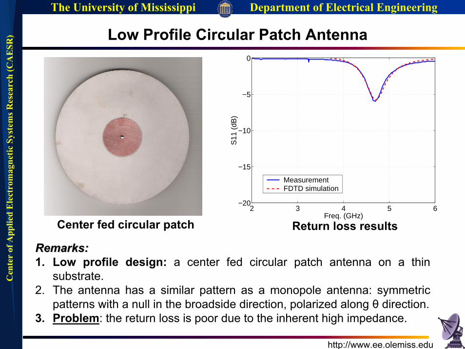
Low Profile Circular Patch Antenna
2 3 4 5 6−20
−15
−10
−5
0
Freq. (GHz)
S11
(dB
)
MeasurementFDTD simulation
Return loss resultsCenter fed circular patch
Remarks:Remarks:1. Low profile design: a center fed circular patch antenna on a thin
substrate.2. The antenna has a similar pattern as a monopole antenna: symmetric
patterns with a null in the broadside direction, polarized along θ direction. 3. Problem: the return loss is poor due to the inherent high impedance.

The University of Mississippi Department of Electrical EngineeringC
ente
r of
App
lied
Ele
ctro
mag
netic
Sys
tem
s Res
earc
h (C
AE
SR)
http://www.ee.olemiss.edu
Patch Fed Surface Wave Antenna: Geometry
y
xTop View
x
z
Cross View
Antenna structure:
1. Grounded substrate: εr = 2.94, t = 3mm, the radius R of the circular ground plane size is 75 mm.
2. Periodic square patch loading: 8 ×8 square patches, w = 7.5 mm, g = 1.5 mm.
3. Center fed circular patch : h = 1.5 mm, r = 21 mm. A feeding probe is connected to its center.

The University of Mississippi Department of Electrical EngineeringC
ente
r of
App
lied
Ele
ctro
mag
netic
Sys
tem
s Res
earc
h (C
AE
SR)
http://www.ee.olemiss.edu
Input Impedance and Return Loss
3 3.5 4 4.5 5 5.5 6−100
−50
0
50
100
150
200
250
Freq. (GHz)
Impe
danc
e (Ω
)
Patch
SWA
3 3.5 4 4.5 5 5.5 6−30
−25
−20
−15
−10
−5
0
Freq. (GHz)
S11
(dB
)
PatchSWA
Input impedanceRemarks:Remarks:1. A center fed patch antenna has an inherent high impedance, resulting in
a poor return loss .2. Because of efficient launching of surface waves, the SWA has a lower Q
factor and the impedance is around 50 Ω at the resonant frequency. Therefore, a very good return loss is observed.
Return loss

The University of Mississippi Department of Electrical EngineeringC
ente
r of
App
lied
Ele
ctro
mag
netic
Sys
tem
s Res
earc
h (C
AE
SR)
http://www.ee.olemiss.edu
Near Field Distributions
Patch antennaRemarks:Remarks:1. The near fields distributions are calculated at the resonant frequencies
and normalized to the E field at the feeding port.2. The surface wave antenna shows stronger E fields than the patch
antenna. For example, near the edge of the ground plane, the E field level of the SWA is about 5 dB higher than that of the patch antenna.
Surface wave antennay (cm)
x (c
m)
|E| (dB)
−30−35
−40
−45−45 −40 −40
−45
−10 −5 0 5 10
−10
−8
−6
−4
−2
0
2
4
6
8
10
−50
−45
−40
−35
−30
−25
−20
−15
−10
−5
0
y (cm)
x (c
m)
|E| (dB)
−30
−35
−40−40 −35 −35
−40
−10 −5 0 5 10
−10
−8
−6
−4
−2
0
2
4
6
8
10
−50
−45
−40
−35
−30
−25
−20
−15
−10
−5
0

The University of Mississippi Department of Electrical EngineeringC
ente
r of
App
lied
Ele
ctro
mag
netic
Sys
tem
s Res
earc
h (C
AE
SR)
http://www.ee.olemiss.edu
Radiation Patterns
−150 −100 −50 0 50 100 150−50
−40
−30
−20
−10
0
10
θ (Degree)
Dire
ctiv
ity (
dB)
Co−polX−pol
−150 −100 −50 0 50 100 150−30
−25
−20
−15
−10
−5
0
5
10
θ (Degree)
Dire
ctiv
ity (
dB)
φ=0φ=45
E plane pattern H plane pattern
Remarks:Remarks:1. Several important observations from the SWA pattern: broadside null,
symmetric patterns, Eθ polarization, low cross polarization.2. H plane pattern is omni-directional.3. The SWA pattern is similar to an actual monopole antenna.
The University of Mississippi Department of Electrical EngineeringC
ente
r of
App
lied
Ele
ctro
mag
netic
Sys
tem
s Res
earc
h (C
AE
SR)
http://www.ee.olemiss.edu
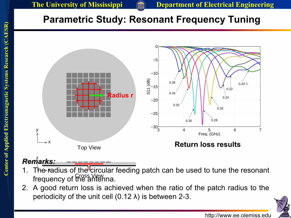
Parametric Study: Resonant Frequency Tuning
3 4 5 6 7−30
−25
−20
−15
−10
−5
0
Freq. (GHz)
S11
(dB
)
0.36
0.34
0.32
0.30 0.28
0.26
0.24
0.22
0.20 λ
y
xTop View
Radius r
Return loss results
xCross View
zRemarks:Remarks:1. The radius of the circular feeding patch can be used to tune the resonant
frequency of the antenna.2. A good return loss is achieved when the ratio of the patch radius to the
periodicity of the unit cell (0.12 λ) is between 2-3.

The University of Mississippi Department of Electrical EngineeringC
ente
r of
App
lied
Ele
ctro
mag
netic
Sys
tem
s Res
earc
h (C
AE
SR)
http://www.ee.olemiss.edu
Parametric Study: Beam Direction Control
−150 −100 −50 0 50 100 150−30
−25
−20
−15
−10
−5
0
5
10
θ (Degree)
Dire
ctiv
ity (
dB)
1.0 λ1.5 λ
y
xTop View
Radius R
Radiation patterns
x
z
Cross View
Remarks:Remarks:1. The radius of the ground plane is used to control beam direction.2. When R is increased from 1 λ4GHz to 1.5 λ4GHz , the return loss remains
similar.3. The antenna beam moves to a low elevation angle, from 46º to 52º. In
addition, more ripples occurs because of the interference of waves.

The University of Mississippi Department of Electrical EngineeringC
ente
r of
App
lied
Ele
ctro
mag
netic
Sys
tem
s Res
earc
h (C
AE
SR)
http://www.ee.olemiss.edu
Parametric Study: Number of Periodic Patches
3 3.5 4 4.5 5 5.5 6−30
−25
−20
−15
−10
−5
0
Freq. (GHz)
S11
(dB
) 4×4 patches
2×2 patches
6×6 patches
8×8 patches10×10 patches
y
xTop View
# of patches
Remarks:1. The center two rows have little effect on return loss. 2. The third and fourth rows, which locate near the edge of exciting
disk, have a significant effect on improving the return loss.3. Adding more rows of patches has little effect on the return loss.
x
z
Cross View

The University of Mississippi Department of Electrical EngineeringC
ente
r of
App
lied
Ele
ctro
mag
netic
Sys
tem
s Res
earc
h (C
AE
SR)
http://www.ee.olemiss.edu
Patch Fed Surface Wave Antenna (SWA): Photo
Middle layer: circular disk Top layer: periodic patches
Remarks:Remarks:1. A circular ground plane with a diameter of 150 mm.2. Middle layer: a circular disk with a center feeding probe.3. Top layer: 8 × 8 periodic square patches.4. RT/Duroid 6002 substrate is used in each layer with εr=2.94 and
thickness of 1.5 mm.

The University of Mississippi Department of Electrical EngineeringC
ente
r of
App
lied
Ele
ctro
mag
netic
Sys
tem
s Res
earc
h (C
AE
SR)
http://www.ee.olemiss.edu
Patch Fed Surface Wave Antenna (SWA): S11
3 3.5 4 4.5 5 5.5 6−30
−25
−20
−15
−10
−5
0
Freq. (GHz)
S11
(dB
)
MeasuredFDTD
3 3.5 4 4.5 5 5.5 6−30
−25
−20
−15
−10
−5
0
Freq. (GHz)
S11
(dB
)
PatchSWA
Patch antenna vs. SWA Measurement vs. FDTD
Remarks:Remarks:1. When the superstrate with periodic patches is stacked on the circular
disk, the resonant frequency shift down (5.12 4.76 GHz) and the return loss of the antenna is significantly improved (-7.9 -28.9 dB).
2. The measured result agrees well with the FDTD simulations.

The University of Mississippi Department of Electrical EngineeringC
ente
r of
App
lied
Ele
ctro
mag
netic
Sys
tem
s Res
earc
h (C
AE
SR)
http://www.ee.olemiss.edu
Patch Fed Surface Wave Antenna (SWA): Pattern
Measurement vs. FDTDMeasured patterns−150 −100 −50 0 50 100 150
−30
−25
−20
−15
−10
−5
0
5
10
θ (Degree)
Gai
n (d
B)
MeasuredFDTD
−150 −100 −50 0 50 100 150−30
−25
−20
−15
−10
−5
0
5
10
θ (Degree)
Gai
n (d
B)
φ=0, co−polφ=0, X−polφ=45, co−polφ=45, X−pol
Remarks:Remarks:1. The SWA generates a monopole type radiation pattern with a 5.6 dB
gain at θ=47º direction.2. The measured radiation pattern agrees well with the FDTD simulated
result.3. The relatively high cross-polarization in the back is due to the
diffraction of the feeding cable.

The University of Mississippi Department of Electrical EngineeringC
ente
r of
App
lied
Ele
ctro
mag
netic
Sys
tem
s Res
earc
h (C
AE
SR)
http://www.ee.olemiss.edu
OUTLINEOverview of metamaterial surfaces
Characterizations and designs
Various EM applications
A simple and efficient FDTD/PBC algorithm
Basic idea: constant kx method
Numerical examples
A low profile surface wave antenna
Antenna concept
Designs and verifications
Conclusions

The University of Mississippi Department of Electrical EngineeringC
ente
r of
App
lied
Ele
ctro
mag
netic
Sys
tem
s Res
earc
h (C
AE
SR)
http://www.ee.olemiss.edu
Meta-Material Surface
Properties of meta-material surfaces
Designs of meta-material surfaces
Surface wave Plane wave
Applications of meta-material surfaces
Patch element
and array
Low profile dipole
Surface wave
antennas
Low profile
monopole
Low profile
curl
Circularly polarized
dipole
Parameter analysis PDEBG designs Vias effects

The University of Mississippi Department of Electrical EngineeringC
ente
r of
App
lied
Ele
ctro
mag
netic
Sys
tem
s Res
earc
h (C
AE
SR)
http://www.ee.olemiss.edu
Various Antennas on Meta-Material Surfaces
Patch element Patch array Bent monopole
Low profile curl CP dipole Surface wave antenna

The University of Mississippi Department of Electrical EngineeringC
ente
r of
App
lied
Ele
ctro
mag
netic
Sys
tem
s Res
earc
h (C
AE
SR)
http://www.ee.olemiss.edu
A Simple and Efficient FDTD/PBC Algorithm
The idea of a novel periodic boundary condition (PBC) are presented for analysis of periodic structures.
By fixing the horizontal wavenumber, the periodic boundary condition can be easily formulated in the FDTD method.
The new approach is simple to implement and efficient for arbitrary incident angles.
The validity of the approach has been demonstrated through several numerical examples.

The University of Mississippi Department of Electrical EngineeringC
ente
r of
App
lied
Ele
ctro
mag
netic
Sys
tem
s Res
earc
h (C
AE
SR)
http://www.ee.olemiss.edu
Low Profile Surface Wave Antenna
Novel surface wave antennas excited by a dipole or a circular disk are introduced in this presentation.
It exhibits a monopole type radiation pattern and a good return loss within an attractive low profile configuration.
An antenna prototype was designed, fabricated, and tested. The antenna resonated at 4.76 GHz with a 5.6% bandwidth. A monopole type pattern with a 5.6 dB gain was obtained.
The proposed antenna has a good potential for wireless communications such as vehicle radio systems.

The University of Mississippi Department of Electrical EngineeringC
ente
r of
App
lied
Ele
ctro
mag
netic
Sys
tem
s Res
earc
h (C
AE
SR)
http://www.ee.olemiss.edu
Acknowledgement
The presenter would like to gratefully thank following colleagues for their collaborations:
• Prof. Yahya Rahmat-Samii, UCLA
• Prof. Ahmed Kishk, The University of Mississippi
• Prof. Atef Elsherbeni, The University of Mississippi
• Prof. Ji Chen, University of Houston
• Prof. Hossein Mosallaei, Northeastern University,
and many other colleagues in UCLA and The University of Mississippi.