Embed Size (px)
Citation preview
MOS-AK/GSA Workshop Fraunhofer IIS, Dresden, April 26-27, 2012
A method for CMOS IC design towards yield optimization
D. Tomaszewski a) , M. Yakupov b) a) Institute of Electron Technology, Warsaw, Poland
b) MunEDA GmbH, Munich, Germany

MOS-AK/GSA Workshop, Fraunhofer IIS, Dresden, April 26-27, 2012 2
Outline
1. Introduction
2. Introductory example (1D, 2D)
3. Cumulative-distribution function-based approach
4. Application of the CDF method for inverter and opamp design
5. Remarks on CDF-based method implementation
6. Conclusion, further work
MOS-AK/GSA Workshop, Fraunhofer IIS, Dresden, April 26-27, 2012 3
v Importance of the yield optimization task o Time-to-market, and cost effectiveness, o Robustness of design;
v Corner (worst case – WC) methods o Fast design space exploration in terms of process and environment
condition (PVT) variations, o Increase of number of corners; some worst-case corners may be
missed, o Lack of correlations between different parameters sets;
v Monte-Carlo (MC) method o Time consuming, many simulations, o Does not actively manipulate / improve a design;
v Worst-case distance (WCD) method o Operates in process parameter space;
v Cumulative distribution function (CDF) – based method o Operates in design parameter space;
Introduction

MOS-AK/GSA Workshop, Fraunhofer IIS, Dresden, April 26-27, 2012 4
Given: length L (design), sheet resistance Rs (model) being a random variable of normal distribution:
Task: Design a resistor, which fulfills the condition: Rmin< R <Rmax;
Find W (design):
Introductory example
)LW
RRLW
R(Pmax
)RWL
RR(Pmax
)RRR(Pmax
maxsminW
maxsminW
maxminW
⋅≤≤⋅
=≤⋅≤
=≤≤
( )σ∝ Rsmean,ss ,RNR

MOS-AK/GSA Workshop, Fraunhofer IIS, Dresden, April 26-27, 2012 5
Conclusions: 1. yield depends on relation between
parameter (R) constraints and process (Rs) quality;
2. cumulative distribution function (CDF) has been successfuly used to determine optimum design.
Introductory example Rmin (Ω) 980 925 800 940 940
Rmax (Ω) 1020 1075 1120 1060 1060
L (m) 1.20E-4 1.20E-4 1.20E-4 1.20E-4 1.20E-4
RS,mean (Ω/sq) 10 10 10 10 13 σRs (Ω/sq) 0.3 0.3 0.3 0.1 0.1
MOS-AK/GSA Workshop, Fraunhofer IIS, Dresden, April 26-27, 2012 6
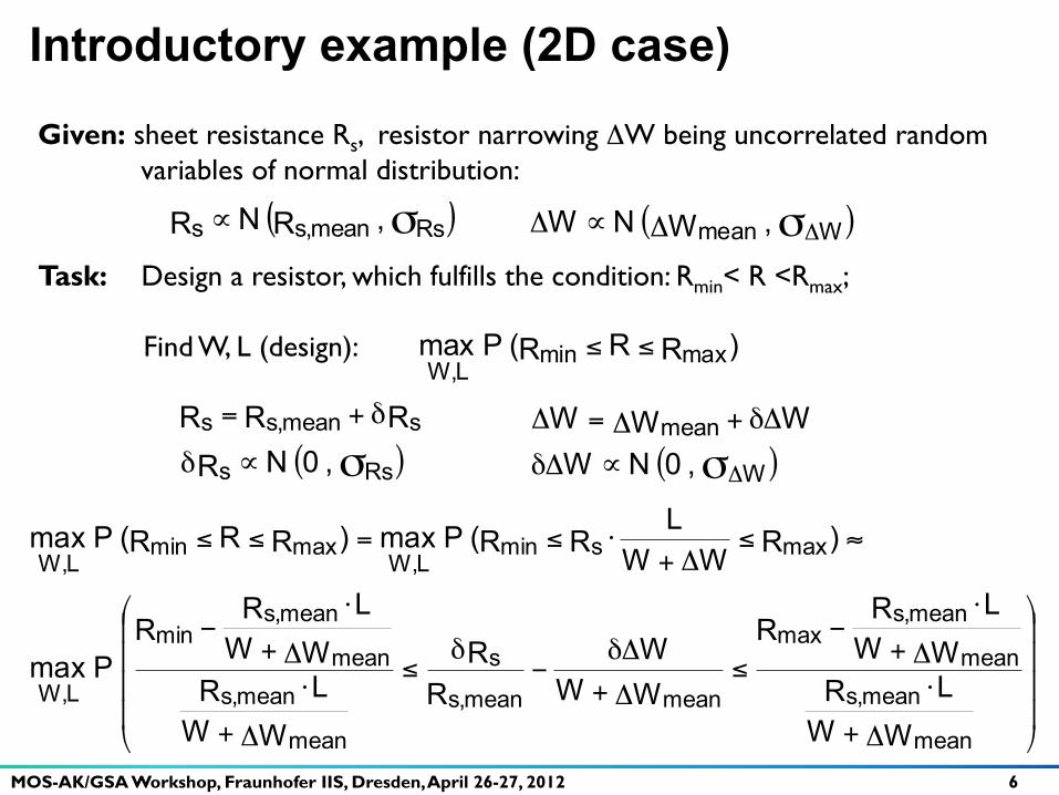
Given: sheet resistance Rs, resistor narrowing ΔW being uncorrelated random variables of normal distribution:
Task: Design a resistor, which fulfills the condition: Rmin< R <Rmax;
Find W, L (design):
Introductory example (2D case)
)RRR(Pmax maxminL,W
≤≤
( )σ∝ Rsmean,ss ,RNR ( )σΔΔ∝Δ Wmean ,WNW
⎟⎟⎟⎟
⎠
⎞
⎜⎜⎜⎜
⎝
⎛
Δ+
⋅Δ+
⋅−
≤Δ+Δδ
−δ
≤
Δ+
⋅Δ+
⋅−
≈≤Δ+
⋅≤=≤≤
WWLRWW
LRR
WWW
RR
WWLRWW
LRR
Pmax
)RWWL
RR(Pmax)RRR(Pmax
mean
mean,smean
mean,smax
meanmean,s
s
mean
mean,smean
mean,smin
L,W
maxsminL,W
maxminL,W
( )σ∝δ
δ+=
Rss
smean,ss
,0NRRRR
( )σΔ∝Δδ
Δδ+Δ=Δ
W
mean,0NW
WWW

MOS-AK/GSA Workshop, Fraunhofer IIS, Dresden, April 26-27, 2012 7
Introductory example (2D)
length
wid
th
Rmin (Ω) 980 940 940 Rmax (Ω) 1020 1060 1060 Rs,mean (Ω/sq) 10 10 10 σRs (Ω/sq) 0.3 0.3 0.1 ΔWmean (m) -2.0E-7 -2.0E-7 -2.0E-7 σΔW (m) 3.0E-8 3.0E-8 1.0E-8
MOS-AK/GSA Workshop, Fraunhofer IIS, Dresden, April 26-27, 2012 8
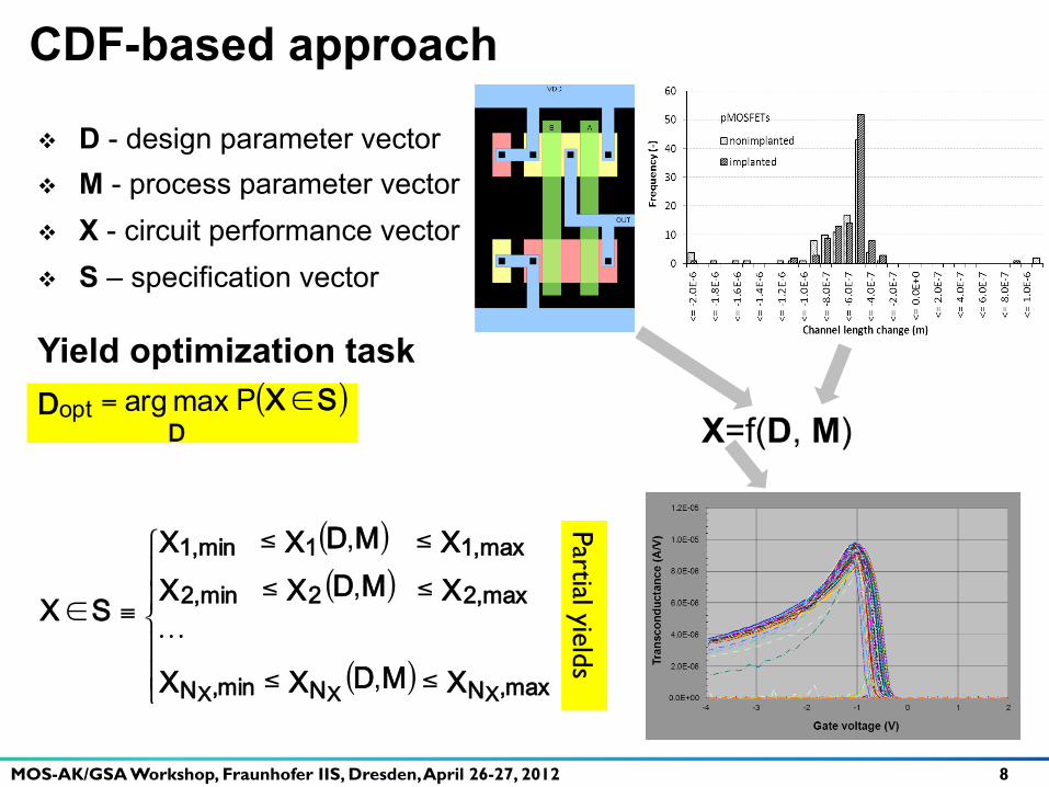
v D - design parameter vector v M - process parameter vector v X - circuit performance vector v S – specification vector
Yield optimization task
CDF-based approach
( )SXDD
∈= Pmaxargopt
( )( )
( )⎪⎪
⎩
⎪⎪
⎨
⎧
≤≤
≤≤
≤≤
≡∈
XMDXX
XMDXXXMDXX
SX
max,NNmin,N
max2,2min2,
max1,1min1,
XXX ,
,,
X=f(D, M) Partial yields

MOS-AK/GSA Workshop, Fraunhofer IIS, Dresden, April 26-27, 2012 9
CDF-based approach ( ) ( ) ( )
( )∑=
δ⋅∂∂
+≈δ+=N
1jj
j
i
,iii
MM
MX,X,X,X
MDMDMMDMD
nom
nomnom
Issues: v To determine Mnom ⇒ performances of the nom. design ⇒ performance sensitivities v To determine δM
Nominal design i-th performance Sensitivities Process par. variations
Remarks: v Relation to BPV method used for statistical modelling, i.e. for extraction of δM – random var.
Dopt should maximize joint probability:
( )( )
( )⎟⎟⎟
⎠
⎞
⎜⎜⎜
⎝
⎛
⎟⎟⎟
⎠
⎞
⎜⎜⎜
⎝
⎛−≤δ⋅
∂∂
≤−= =
∑N
,XXMMX,XXP
X M
1iimax,i
N
1jj
j
i
,imin,i MDMD
MDnomnom
nomIssues: v Select reliable method for yield
optimization
Remarks: v An optimization problem has
been formulated

MOS-AK/GSA Workshop, Fraunhofer IIS, Dresden, April 26-27, 2012 10
CDF-based approach
If Mj are uncorrelated normally-distributed random variables, then
( )( )
( )∑σσ∑==
σ⋅⎟⎟⎟
⎠
⎞
⎜⎜⎜
⎝
⎛
∂∂
=∝δ⋅∂∂
=N
1j
2
j
i
,
2
2YY
N
1jj
j
i
,
M
j
M
MMX,,0NM
MXY
MDMD nomnom
I.
Issues: v Select uncorrelated process parameters v Process parameters not normally distributed
Due to the unavoidable correlation between performances, direct yield and product of partial yields are not equal.
( )( ) ( )( )∏==
≤≤≠⎟⎟⎠
⎞⎜⎜⎝
⎛≤≤
NN
i
xx,,
1imaxi,imini,
1maxi,imini, XMDXXPXMDXXP
II.
( )( ) ( )( )∏==
≤≤=⎟⎟⎠
⎞⎜⎜⎝
⎛≤≤
NN
i
xx,,
1imaxi,imini,
1maxi,imini, XMDXXPXMDXXP
Issue: Account for correlations between performances, or assume, that
MOS-AK/GSA Workshop, Fraunhofer IIS, Dresden, April 26-27, 2012 11
CDF-based approach
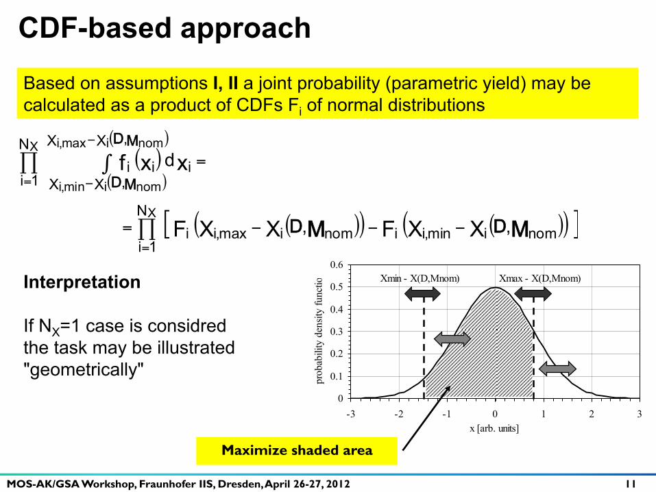
Based on assumptions I, II a joint probability (parametric yield) may be calculated as a product of CDFs Fi of normal distributions
( )( )
( )
( )( ) ( )( )[ ]∏
∏ ∫
=
=
−
−
−−−=
=
N
1inomimin,iinomimax,ii
N
1i
,XX
,XXiii
X
X nomimax,i
nomimin,i
,,
d
XXFXXF
xxf
MM DD
MD
MD
0
0.1
0.2
0.3
0.4
0.5
0.6
-3 -2 -1 0 1 2 3x [arb. units]
prob
abili
ty d
ensit
y fu
nctio
n Xmax - X(D,Mnom)Xmin - X(D,Mnom)Interpretation If NX=1 case is considred the task may be illustrated "geometrically"
Maximize shaded area
MOS-AK/GSA Workshop, Fraunhofer IIS, Dresden, April 26-27, 2012 12
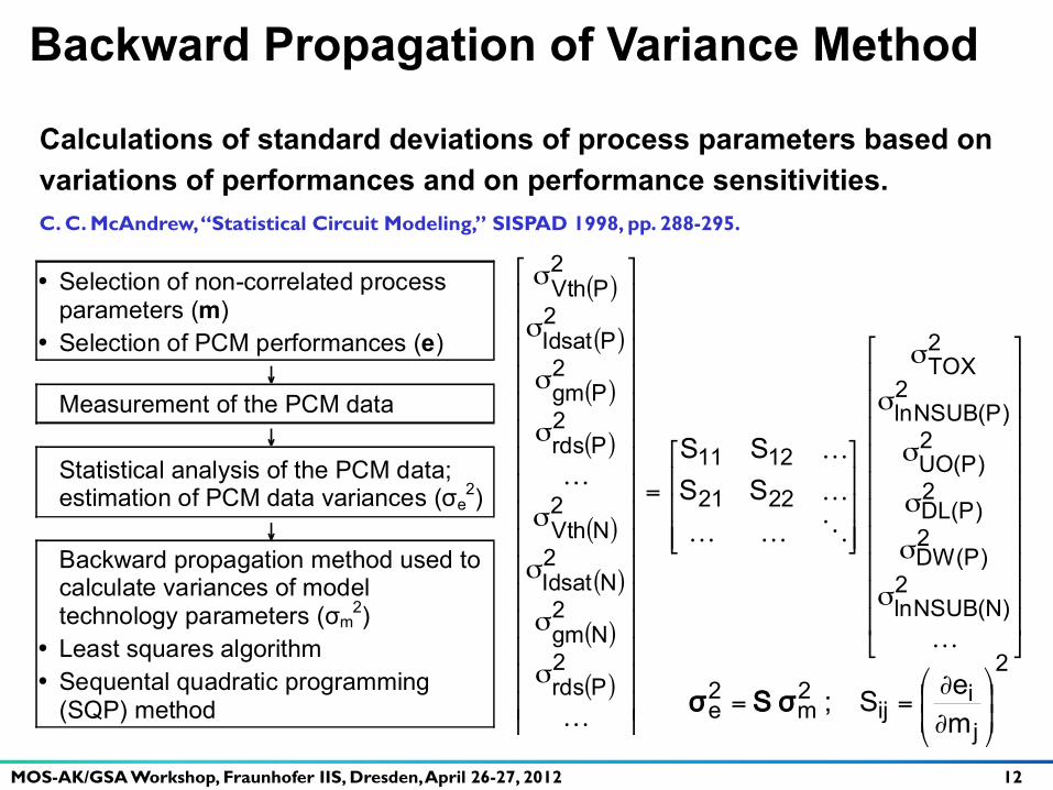
Calculations of standard deviations of process parameters based on variations of performances and on performance sensitivities.
( )
( )
( )
( )
( )
( )
( )
( )
⎥⎥⎥⎥⎥⎥⎥⎥⎥⎥
⎦
⎤
⎢⎢⎢⎢⎢⎢⎢⎢⎢⎢
⎣
⎡
σ
σ
σ
σ
σ
σ
⎥⎥⎥
⎦
⎤
⎢⎢⎢
⎣
⎡=
⎥⎥⎥⎥⎥⎥⎥⎥⎥⎥⎥⎥⎥⎥⎥⎥
⎦
⎤
⎢⎢⎢⎢⎢⎢⎢⎢⎢⎢⎢⎢⎢⎢⎢⎢
⎣
⎡
σ
σ
σ
σ
σ
σ
σ
σ
…
…………
…
…
2)N(NSUBln
2)P(DW
2)P(DL
2)P(UO
2)P(NSUBln
2TOX
2221
1211
2Prds
2Ngm
2NIdsat
2NVth
2Prds
2Pgm
2PIdsat
2PVth
SSSS
Backward Propagation of Variance Method
C. C. McAndrew, “Statistical Circuit Modeling,” SISPAD 1998, pp. 288-295.
• Selection of non-correlated process parameters (m)
• Selection of PCM performances (e) ↓
Measurement of the PCM data ↓
Statistical analysis of the PCM data; estimation of PCM data variances (σe
2) ↓
Backward propagation method used to calculate variances of model technology parameters (σm
2) • Least squares algorithm • Sequental quadratic programming
(SQP) method ⎟⎟⎠
⎞⎜⎜⎝
⎛
∂∂
==ji2
ij2m
2e m
eS;σSσ

MOS-AK/GSA Workshop, Fraunhofer IIS, Dresden, April 26-27, 2012 13
CDF-based approach vs BPV method
Functional block performance variances determined experimentally
Functional block performance (PCM) sensitivities @ nominal process parameters
Process parameter variances
BPV
CDF of functional block performance variances
Functional block performance sensitivities @ nominal process parameters
Process parameter variances

MOS-AK/GSA Workshop, Fraunhofer IIS, Dresden, April 26-27, 2012 14
CDF method - Inverter
Inverter performances J.P.Uemura, "CMOS Logic Circuit Design", Kluwer, 2002
ββ+
⋅ββ+−=
pn
n,Tpnp,TDDI 1
VVVV
( )tt5.0t
CR1VVV
4lnVV
V2t
CR1VVV4ln
VVV2
t
LH,PHL,PP
outpDD
p,TDD
p,TDD
p,TLH,P
outnDD
n,TDD
n,TDD
n,THL,P
+⋅=
⋅⋅⎥⎥⎦
⎤
⎢⎢⎣
⎡
⎟⎟
⎠
⎞
⎜⎜
⎝
⎛−
−+
−=
⋅⋅⎥⎦
⎤⎢⎣
⎡⎟⎟⎠
⎞⎜⎜⎝
⎛−
−+
−=
( )VVII IinDDmax,DD ==
Inverter threshold
Propagation delay

MOS-AK/GSA Workshop, Fraunhofer IIS, Dresden, April 26-27, 2012 15
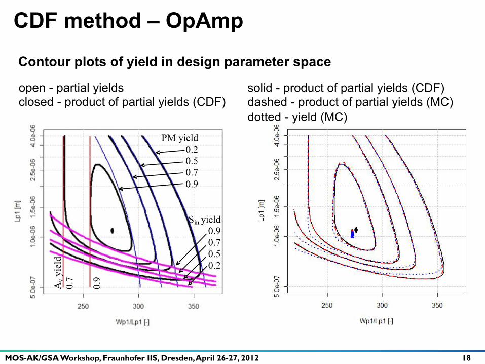
CDF method – OpAmp
∑= ⎟
⎟
⎠
⎞
⎜⎜
⎝
⎛ω−Π=4
1j j
cp
tgarcPM
⎟⎟⎠
⎞⎜⎜⎝
⎛
+⋅⎟⎟⎠
⎞⎜⎜⎝
⎛
+=
ggg
ggg
A7o6o
6m
4o2o
2mv
( )SSgg
SSS 24
23
1m
3m2
22
21
2in +⋅⎟⎟
⎠
⎞⎜⎜⎝
⎛++=
OpAmp performances M.Hershenson, et al.,"Optimal Design of a CMOS Op-Amp via Geometric Programming", IEEE Trans. CAD ICAS, Vol.20, No.1
Low-frequency gain
Phase margin
Equivalent input-referred noise power spectral density
• gmi, goi - input and output conductances of i-th transistor,
• ωc is a unity-gain bandwidth, • pj - j-th pole of the circuit, • Sk - input-referred noise power
spectral densities, consisting of thermal and 1/f components.

MOS-AK/GSA Workshop, Fraunhofer IIS, Dresden, April 26-27, 2012 16
CDF method – Inverter, OpAmp
• Monte-Carlo method 1000 samples
• simple MOSFET model • 0.8 µm CMOS technology
o tox=20 nm, o Vthn=0.7 V, Vthp=-0.9 V
• process parameters varied: o gate oxide thickness
tox, o substrate doping conc.
Nsubn, Nsubp, o carrier mobilities
µon, µop, o fixed charge densities
Nssn, Nssp

MOS-AK/GSA Workshop, Fraunhofer IIS, Dresden, April 26-27, 2012 17
Contour plots of yield in design parameter space
tP yield 0.2 0.9
IDDmax yield 0.8 0.4 0.2
CDF method - Inverter
open - partial yields closed - product of partial yields (CDF)
solid - product of partial yields (CDF) dashed - product of partial yields (MC) dotted - yield (MC)
A "valley" results from the specification of tP,min constrain.
MOS-AK/GSA Workshop, Fraunhofer IIS, Dresden, April 26-27, 2012 18
Av y
ield
0.
7 0.9
PM yield 0.2 0.5 0.7 0.9
Sin yield 0.9 0.7 0.5 0.2
CDF method – OpAmp
Contour plots of yield in design parameter space
open - partial yields closed - product of partial yields (CDF)
solid - product of partial yields (CDF) dashed - product of partial yields (MC) dotted - yield (MC)

MOS-AK/GSA Workshop, Fraunhofer IIS, Dresden, April 26-27, 2012 19
CDF-based method implementation
Objective function maximization v Close to the maximum the objective function may exhibit a plateau;
Optimization task based on gradient approach requires in this case 2nd order derivatives of yield function, but…
this makes optimization based on gradient methods useless;

MOS-AK/GSA Workshop, Fraunhofer IIS, Dresden, April 26-27, 2012 20
CDF-based method implementation
Objective function maximization v Objective function may exhibit more than one plateau or more local
maxima;
thus
v a non-gradient global optimization method is required.

MOS-AK/GSA Workshop, Fraunhofer IIS, Dresden, April 26-27, 2012 21 21
1. The presented CDF-based method may be used for IC block design optimizing parametric yield,
2. The method may predict parametric yield of the design, 3. The design rules of the given IP and also discrete set of allowed
solutions* may be directly used and shown in the yield plots in the design parameter space,
4. The method may be very useful for evaluation if the process is efficient enough to achieve a given yield,
5. The CDF-based method gives results, which are very close to the Monte Carlo method,
6. The results of yield optimization (Yopt) based on CDF method have direct interpretation in design parameter space (problem of selection of design parameters: explicit or combined),
Conclusions, further work (1)
* Pierre Dautriche, "Analog Design Trends & Challenges in 28 and 20 nm CMOS Technology", ESSDERC'2011

MOS-AK/GSA Workshop, Fraunhofer IIS, Dresden, April 26-27, 2012 22 22
7. If the performance constraints are mild with respect to process variability, a continuous set of design parameters, for which yield close to 100% is expected,
8. If the constraints are severe with respect to process variability, the method leads to unique solution, for which the parametric yield below 100% is expected,
9. The method may be used for performances determined both analytically, as well as via Spice-like simulations (batch mode) – to be done,
10. Method should be developed to take into account performance correlations and non-gaussian distributions – to be done,
11. The methodology may be used for design types (not only of ICs) taking into account statistical variability of a process and aimed at yield optimization.
Conclusions, further work (2)

MOS-AK/GSA Workshop, Fraunhofer IIS, Dresden, April 26-27, 2012 23
Acknowledgement
Financial support of EC within project PIAP-GA-2008-218255 ("COMON") partial financial support (for presenter) of EC within project ACP7-GA-2008-212859 ("TRIADE") Assistance of Dr.Grzegorz Gluszko (ITE) at the measurements are acknowledged.