Embed Size (px)
Citation preview

A Low-power Area-efficient Switching Scheme for Charge-sharing DACs in SAR ADCs
Fred Chen, Anantha P. Chandrakasan, and Vladimir Stojanović Department of EECS, Massachusetts Institute of Technology, Cambridge, MA 02139, USA
Abstract—Analysis and experimental results for a new
switching scheme and topology for charge sharing DACs used in successive approximation register (SAR) ADCs is presented. The characteristics of the SAR algorithm are exploited to develop a switching scheme that reduces the number of required unit capacitors by nearly an order of magnitude over conventional charge sharing DACs without the aid of any additional reference voltages. The proposed topology also enables a rail-to-rail voltage swing at the DAC output enabling a differential voltage input at the ADC of up to twice the supply voltage. An 8-bit SAR ADC using the proposed DAC is implemented in a 90nm CMOS process and consumes 700 nW at 0.7 V and 100 kS/s while occupying 0.0135 mm2.
I. INTRODUCTION The SAR ADC architecture [1] has become a popular
topology for low-to-medium resolution, low-speed and low-power applications because of its low analog complexity and amenability towards voltage scaling in scaled CMOS processes [2]. Consequently, a growing number of systems ranging from biomedical to power management applications are integrating multiple ADCs for monitoring purposes [3-5].
In emerging biomedical applications such as wireless implantable neural recorders, the energy constraints are strict, while the sampling frequencies (<200kS/s) and required resolutions (6-10 bits) are modest. Thus, the SAR ADC architecture is a sensible and widely adopted choice for use in digitizing sensor data in these systems [3, 4]. In these multi-channel systems, the bandwidth of each channel is low, so a common strategy used for integration is to time-multiplex the ADC across many amplifiers. However, as shown in Fig. 1, the drawback of this approach is that the power overhead associated with multiplexing in the analog domain can be dominant [4]; both the buffers and the analog multiplexing circuitry must maintain signal linearity to the ADC and require relatively high power to do so. Alternatively, if the efficiency of the ADC could be leveraged such that there was a separate ADC per channel, and multiplexing was performed in the digital domain, the power per channel as well as the system complexity could be reduced. However, this approach is typically impractical if not impossible because of area constraints. For resolutions in the 8-10 bit range, the ADC area far outweighs the area of the amplifiers, but if the area overhead could be reduced, then system power savings could be realized by integrating more ADCs.
In this work, we present analysis and experimental results for an alternative DAC topology and switching scheme that relies on only a 1:1 capacitor ratio and leverages the inherent memory of the SAR switching algorithm to reduce the total
number of capacitors needed with minimal conversion cycle overhead. Unlike previous schemes to reduce the DAC capacitor array [6, 7], the proposed approach does not require any additional reference voltage and is not sensitive to specific ratios of parasitic capacitances. The proposed switching scheme also utilizes charge recycling to reduce the power and is capable of outputs spanning the full supply voltage. The following sections will first give a brief background on charge- sharing SAR ADCs and then describe the proposed switching scheme. The remaining sections will provide some analysis, simulated and measured results, and conclusions.
II. CHARGE-REDISTRIBUTION SAR ADCS Fig. 2 shows the block diagram and an example of the SAR
conversion algorithm as originally proposed [1] while Fig. 3a shows the corresponding charge-redistribution DAC used to generate the reference levels during the conversion. The conventional redistribution DAC relies on ratios of binary weighted capacitors to generate the intermediate voltage levels between a reference voltage, VREF, and ground. As many works have noted, the original charge sharing topology is inefficient in its use of charge and incurs an exponential area and power penalty as the resolution of the ADC increases [6-8].
This shortcoming was also recognized by the original authors who offered an alternative implementation of the charge- redistribution DAC (Fig. 3b) that requires only two nominally identical capacitors [9]. Each output voltage level is generated by sequentially pre-charging or discharging C1 and then connecting C1 to C2 in order to incrementally add or subtract charge from C2. While the binary weighted capacitor scheme requires exponentially more unit capacitors as the resolution of the ADC increases, the drawback for the serial DAC based ADC is that the number of internal conversion cycles increases exponentially with the ADC resolution. Consequently, it is exponentially slower as the ADC resolution increases.
Fig. 1. Block diagram of a sample time-multiplexed neural recording front end with annotated power consumption per circuit [4]
Fig. 2. An example of a SAR ADC conversion and circuit block diagram
Cb-2Cb-1Cb C0C1C2
VREF
Cb=2bC0
C0
VX
(a) (b)
VREFC1=C2
C2
VX
C1
Fig. 3. (a) A conventional binary weighted charge-redistribution DAC used in SAR ADCs . (b) A serial charge-redistribution DAC first proposed in [9].
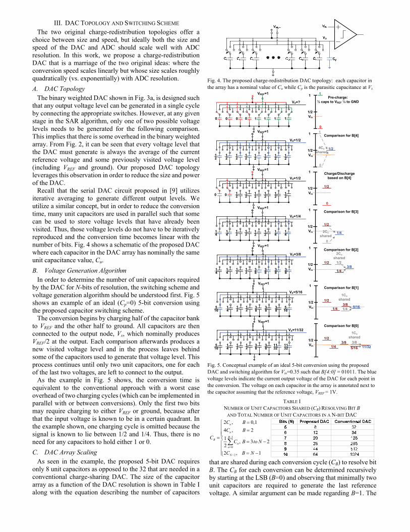
III. DAC TOPOLOGY AND SWITCHING SCHEME The two original charge-redistribution topologies offer a
choice between size and speed, but ideally both the size and speed of the DAC and ADC should scale well with ADC resolution. In this work, we propose a charge-redistribution DAC that is a marriage of the two original ideas: where the conversion speed scales linearly but whose size scales roughly quadratically (vs. exponentially) with ADC resolution. A. DAC Topology
The binary weighted DAC shown in Fig. 3a, is designed such that any output voltage level can be generated in a single cycle by connecting the appropriate switches. However, at any given stage in the SAR algorithm, only one of two possible voltage levels needs to be generated for the following comparison. This implies that there is some overhead in the binary weighted array. From Fig. 2, it can be seen that every voltage level that the DAC must generate is always the average of the current reference voltage and some previously visited voltage level (including VREF and ground). Our proposed DAC topology leverages this observation in order to reduce the size and power of the DAC.
Recall that the serial DAC circuit proposed in [9] utilizes iterative averaging to generate different output levels. We utilize a similar concept, but in order to reduce the conversion time, many unit capacitors are used in parallel such that some can be used to store voltage levels that have already been visited. Thus, those voltage levels do not have to be iteratively reproduced and the conversion time becomes linear with the number of bits. Fig. 4 shows a schematic of the proposed DAC where each capacitor in the DAC array has nominally the same unit capacitance value, Cu. B. Voltage Generation Algorithm
In order to determine the number of unit capacitors required by the DAC for N-bits of resolution, the switching scheme and voltage generation algorithm should be understood first. Fig. 5 shows an example of an ideal (Cp=0) 5-bit conversion using the proposed capacitor switching scheme.
The conversion begins by charging half of the capacitor bank to VREF and the other half to ground. All capacitors are then connected to the output node, Vx, which nominally produces VREF/2 at the output. Each comparison afterwards produces a new visited voltage level and in the process leaves behind some of the capacitors used to generate that voltage level. This process continues until only two unit capacitors, one for each of the last two voltages, are left to connect to the output.
As the example in Fig. 5 shows, the conversion time is equivalent to the conventional approach with a worst case overhead of two charging cycles (which can be implemented in parallel with or between conversions). Only the first two bits may require charging to either VREF or ground, because after that the input voltage is known to be in a certain quadrant. In the example shown, one charging cycle is omitted because the signal is known to lie between 1/2 and 1/4. Thus, there is no need for any capacitors to hold either 1 or 0. C. DAC Array Scaling
As seen in the example, the proposed 5-bit DAC requires only 8 unit capacitors as opposed to the 32 that are needed in a conventional charge-sharing DAC. The size of the capacitor array as a function of the DAC resolution is shown in Table I along with the equation describing the number of capacitors
that are shared during each conversion cycle (CB) to resolve bit B. The CB for each conversion can be determined recursively by starting at the LSB (B=0) and observing that minimally two unit capacitors are required to generate the last reference voltage. A similar argument can be made regarding B=1. The
Fig. 4. The proposed charge-redistribution DAC topology: each capacitor in the array has a nominal value of Cu while Cp is the parasitic capacitance at Vx.
VREF=1
VX=1/2
VREF=1
0 0 0 1 1 1
VX=?
0 1
VREF=1
0 0
VX=1/2
12
12
12
12
12
12
12
12
12
12
12
12
12
12
VREF=1
VX=1/4
12
12
12
12
14
14
14
14
VREF=1
VX=3/8
12
12
38
38
38
38
14
14
1/2
1
1/2
1/4
2Cushared
3/81/2
1/2
1
1/2
1
0
4Cushared
1/2
1
1/2
0
1/2
1
1/2
0
1/42Cushared
Vin
Vin
Vin
Vin
VREF=1
VX=5/16
12
12
38
38
38
516
516
14
VREF=1
VX=11/32
12
12
38
38
1132
1132
516
14
1/2 1/2
1/4
1Cushared
3/85/16
Vin 11/32
1
1/2
1
0
Vin
3/8
Pre-charge: ½ caps to VREF ½ to GND
Comparison for B[4]
Charge/Discharge based on B[4]
Comparison for B[3]
Comparison for B[2]
Comparison for B[1]
Comparison for B[0]
1
1/2 1/2
1/4
1Cushared
3/81/4 5/16Vin
Fig. 5. Conceptual example of an ideal 5-bit conversion using the proposed DAC and switching algorithm for Vin=0.35 such that B[4:0] = 01011. The blue voltage levels indicate the current output voltage of the DAC for each point in the conversion. The voltage on each capacitor in the array is annotated next to the capacitor assuming that the reference voltage, VREF = 1V.
TABLE I NUMBER OF UNIT CAPACITORS SHARED (CB) RESOLVING BIT B
AND TOTAL NUMBER OF UNIT CAPACITORS IN A N-BIT DAC
1
0
2
2 , 0,14 , 21 , 3 222 , 1
u
u
BB
nn
N
C BC B
CC B to N
C B N
−
=
−
=⎧⎪ =⎪⎪= ⎨ = −⎪⎪
= −⎪⎩
∑
number of capacitors required for all of the preceding bits follows the general rule that at each voltage level, enough capacitors must be used for storing that voltage level to enable voltage generation for less significant bits. The equation for bits 3 to N-2 in Table I results because each stored voltage level only has to provide half of the capacitors shared during any comparison. Finally, the total number of capacitors for an N-bit DAC, CN-1, results from having to generate VREF/2 from the supply rails which requires an equal number of capacitors, thus the factor of 2.
IV. DAC DESIGN CONSIDERATIONS The preceding discussion regarding the DAC has assumed
idealized conditions. However, like many other charge-sharing techniques, the proposed topology is not impervious to parasitics and other non-idealities. In this section, we will discuss some of the design considerations and limitations of the proposed architecture. A. Capacitor Parasitics
In the proposed DAC topology, there are only switches on one side of the capacitor array so the only node at which parasitics are a concern is at the top plate of the capacitor. Since the other end of the capacitor is attached to ground, any stray parasitics to ground will simply add to the nominal value of Cu provided that it is the same for every element in the array. However, since the node, Vx, is not actively driven during a conversion cycle, any parasitic capacitance (Cp in Fig. 4) at that node will introduce error in the conversion. The DAC output voltage generated for each comparison can be calculated as: ( )
( ), 1 , , 1
, 2B x n x n N p x n
x nB p
C V V C VV
C C− − −+ +
=⋅ +
(1)
where CB is the number of shared unit capacitors defined in Table I and Cp is the parasitic capacitance at node Vx. In (1), Vx,n is the next voltage level to be generated, while Vx,n-1 was the last voltage level generated, and Vx,n-N is some previously visited voltage level such that Vx,n-N – Vx,n=VREF/2n. Thus, if Cp=0, each voltage generated is exactly the average of two previous states.
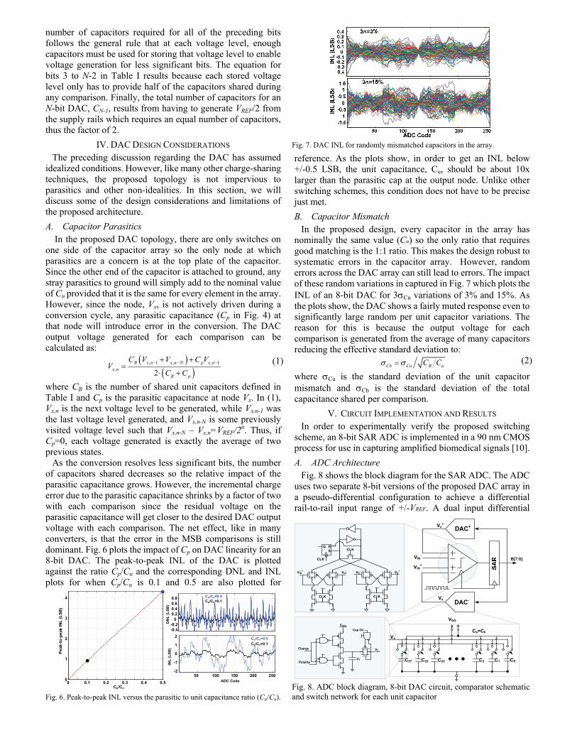
As the conversion resolves less significant bits, the number of capacitors shared decreases so the relative impact of the parasitic capacitance grows. However, the incremental charge error due to the parasitic capacitance shrinks by a factor of two with each comparison since the residual voltage on the parasitic capacitance will get closer to the desired DAC output voltage with each comparison. The net effect, like in many converters, is that the error in the MSB comparisons is still dominant. Fig. 6 plots the impact of Cp on DAC linearity for an 8-bit DAC. The peak-to-peak INL of the DAC is plotted against the ratio Cp/Cu and the corresponding DNL and INL plots for when Cp/Cu is 0.1 and 0.5 are also plotted for
reference. As the plots show, in order to get an INL below +/-0.5 LSB, the unit capacitance, Cu, should be about 10x larger than the parasitic cap at the output node. Unlike other switching schemes, this condition does not have to be precise just met. B. Capacitor Mismatch
In the proposed design, every capacitor in the array has nominally the same value (Cu) so the only ratio that requires good matching is the 1:1 ratio. This makes the design robust to systematic errors in the capacitor array. However, random errors across the DAC array can still lead to errors. The impact of these random variations in captured in Fig. 7 which plots the INL of an 8-bit DAC for 3σCu variations of 3% and 15%. As the plots show, the DAC shows a fairly muted response even to significantly large random per unit capacitor variations. The reason for this is because the output voltage for each comparison is generated from the average of many capacitors reducing the effective standard deviation to:
Cb Cu B uC Cσ σ= (2)
where σCu is the standard deviation of the unit capacitor mismatch and σCb is the standard deviation of the total capacitance shared per comparison.
V. CIRCUIT IMPLEMENTATION AND RESULTS In order to experimentally verify the proposed switching
scheme, an 8-bit SAR ADC is implemented in a 90 nm CMOS process for use in capturing amplified biomedical signals [10]. A. ADC Architecture
Fig. 8 shows the block diagram for the SAR ADC. The ADC uses two separate 8-bit versions of the proposed DAC array in a pseudo-differential configuration to achieve a differential rail-to-rail input range of +/-VREF. A dual input differential
Cp/Cu
Peak
-to-p
eak
INL
(LSB
)
0
1
2
3
4
0 0.1 0.2 0.3 0.4 0.5 ADC Code
INL
(LSB
)
-2
-1
0
1
2-0.4-0.2
00.20.40.60.8
50 100 150 200 250
DN
L (L
SB)
Cp/Cu=0.1Cp/Cu=0.5
Cp/Cu=0.5Cp/Cu=0.1
Fig. 6. Peak-to-peak INL versus the parasitic to unit capacitance ratio (Cp/Cu).
Fig. 7. DAC INL for randomly mismatched capacitors in the array.
VDD
A
C0C1C2C25C26C27
Vx
Cb=C0
Charge
VDDA
C0Polarity
Cap On
VX
VIN+
DAC-
B[7:0]VIN-
DAC+
Vx-
Vx+
CLK
CLKRQS
CLK
VIN+ VX
+VX-VIN
-
CLK
Fig. 8. ADC block diagram, 8-bit DAC circuit, comparator schematicand switch network for each unit capacitor

comparator is used to resolve the bits across the large range of inputs and besides transistor leakage, the entire design draws no static current. The 8-bit conversion is implemented with 12 internal ADC cycles and each unit capacitor (Cu), realized with vertical wire capacitors, is nominally 100fF. B. ADC Area and Power
The chip die photo and block layout are shown in Fig. 9. The entire differential ADC occupies less than 150 μm x 90 μm in a 90 nm CMOS process. The remaining results are reported for the ADC operating at 0.7 V (VREF and VDD) at which it consumes 700 nW for a sampling frequency of 100 kS/s.
As the example in Fig. 5 showed, there is a residual charge left in the DAC array after each conversion so the energy required to recharge the DAC is dependent on the previous code value. Fig. 10 plots this code dependent energy per conversion over the range of DAC Codes. In the differential implementation the DACs are both preset to whichever rail they are closer to and then shorted to one another to generate the first voltage level. Thus, only one of the two DACs is drawing energy from the supply for each conversion. Assuming a uniform set of conversion codes, roughly 30 nW of the 700 nW of power can be attributable to the DAC array. C. Measured ADC Performance
Due to miscalculations and some careless layout during design time there were unaccounted for parasitics at the DAC output node, Vx. Similarly, the bandwidth of the sample and hold circuits were limited to less than 3 kHz at the measured operating voltages. These circuit errors obscured our ability to test the ADC and the DAC to its potential and limited the perceived performance of this topology. However, the measured results do correlate well with simulations suggesting that there is a clear path to correcting many of these errors.
The INL and DNL performance of the DAC are measured and plotted in Fig. 11 along with the simulated INL and DNL for a Cp value of 57 fF (which was found through simulation). As the plots show, there is good predictability from the simulated and analytic results. Because of the miscalculation in choosing Cu, the +/-4 LSB of INL error immediately reduces the effective resolution of the ADC to about 5 bits.
This result is confirmed by the measured results for SNR, SNDR and SFDR in Fig. 12 which show an ENOB of about 4.5 bits. As described earlier, the sampling bandwidth of the
sample and hold circuit was limited to less than 3 kHz and this can be seen in the SNDR plot versus the input frequency. Also, as seen in the SNDR plot versus sampling frequency, there is a low end limit to sampling frequency due to device leakage.
VI. CONCLUSION Despite all of the egregious circuit design shortcomings, the
FOM for the ADC, assuming that the sample and hold circuit is limiting frequency is still 310 fJ/conversion step for an ENOB of only 4.5 bits. Since the power in the DAC array is relatively negligible, sizing up the unit capacitor by a factor of 5 and optimizing the aspect ratio of the capacitors would recover at least 2 bits of resolution without significant impact on the total power. Even with 5x larger capacitors, the area of this design is still less than a conventional 8-bit design using 1fF unit capacitors [11]. The energy results along with the clear area advantages suggest that this topology merits further exploration for low-power and low-area applications.
REFERENCES [1] J. McCreary and P. Gray, "All-MOS charge redistribution
analog-to-digital conversion techniques. I," IEEE JSSC, 1975. [2] S. Gambini and J. Rabaey, "Low-Power Successive Approximation
Converter With 0.5 V Supply in 90 nm CMOS," IEEE JSSC, 2007. [3] R. Harrison, P. Watkins, R. Kier, R. Lovejoy, D. Black, B. Greger, and F.
Solzbacher, "A low-power integrated circuit for a wireless 100-electrode neural recording system," IEEE JSSC, vol. 42, 2007, p. 123–133.
[4] M. Chae, W. Liu, Z. Yang, T. Chen, J. Kim, M. Sivaprakasam, and M. Yuce, "A 128-Channel 6mW Wireless Neural Recording IC with On-the-Fly Spike Sorting and UWB Transmitter," ISSCC, 2008.
[5] D. Aksin, et al., "An 11 Bit Sub-Ranging SAR ADC with Input Signal Range of Twice Supply Voltage," 2007 IEEE ISCAS, 2007.
[6] S. Chang and E. Yoon, "A low-power area-efficient 8 bit SAR ADC using dual capacitor arrays for neural microsystems.,"IEEE EMBS, 2009.
[7] E. Alpman, H. Lakdawala, L.R. Carley, and K. Soumyanath, "A 1.1V 50mW 2.5GS/s 7b Time-Interleaved C-2C SAR ADC in 45nm LP Digital CMOS," ISSCC, 2009, pp. 76-78.
[8] B. Ginsburg and A. Chandrakasan, "An Energy-Efficient Charge Recycling Approach for a SAR Converter With Capacitive DAC," 2005 IEEE ISCAS, 2005, pp. 184-187.
[9] R. Suarez, P. Gray, and D. Hodges, "All-MOS charge-redistribution analog-to-digital conversion techniques. II," IEEE JSSC, 1975.
[10] F. Chen, et al., “A Signal-agnostic Compressed Sensing Acquisition System for Wireless and Implantable Sensors,” (unpublished).
[11] P. Harpe, et al., "A 30fJ/Conversion-Step 8b 0-to-10MS/s Asynchronous SAR ADC in 90nm CMOS," ISSCC, 2010.
2mm
90
m
Buf
fers
Fig. 9. Chip die photo and circuit layout showing the ADC area.
Fig. 10. ADC power and DAC energy/conversion vs. DAC code
Fig. 11. INL and DNL of the 8-bit ADC at 0.7V and 100kS/s
0.1 1 1010
15
20
25
30
35
40
45
Input frequency (kHz)
SNR
, SN
DR
, SFD
R (d
B)
SNDR
SNR
SFDR
fs=100kS/s1 10 100
10
15
20
25
30
35
40
45
Sampling frequency (kHz)
SNR
,SN
DR
,SFD
R (d
B)
fin=100Hz
SNDR
SNR
SFDR
Fig. 12. SNR,SNDR, and SFDR vs. input and sampling frequency.