Embed Size (px)
Citation preview

123
ITE Trans. on MTA Vol. 4, No. 2, pp. 123-128 (2016)
1. Introduction
Recently, image sensors with the PDAF function at
image plane has been developed 1), 2). These image
sensors realize the AF function by arranging exclusive
pixels to detect the phase-difference. In these image
sensors, a pair of partially light shielded PD is arranged
in a part of pixel array. The focusing speed is extremely
fast in comparison with conventional contrast detection
AF. The sensitivity, however, is degraded by the light
shielding structure and interpolation processing by
neighboring pixels is necessary for image generation 2).
Therefore, the number of pixels for AF function is
limited to avoid the deterioration of image quality.
In this work, we developed an image sensor with the
imaging and the PDAF functions in all the effective
pixels without exclusive pixel for AF function. All the
effective pixels have two PDs each to detect phase-
difference in one pixel without partially light shielding
structure. Therefore, one pixel works as one AF point,
and the sum of two PD outputs equals one pixel output.
2. Principle of PDAF
Fig. 1 shows the principle of the PDAF function. Exit
pupil of a taking lens and a PD of the image sensor are
in optically conjugate relation by on-chip micro-lens
(ML). Therefore, each pixel by separating into two PDs
Abstract In this paper, we describe a device structure and optical design for a CMOS image sensor with
phase-difference detection photodiodes (PD) for autofocus (AF) function. The individual pixel of this image sensor
is composed of two horizontally displaced PDs separated by a PN junction. All the effective pixels function as
both the imaging and the phase-difference detection AF (PDAF). We have realized a low dark random noise
(1.8e- at 1PD, 2.5e- at 1pixel) and high sensitivity (78Ke-/lx.sec at 1green pixel) image sensor with the imaging
and the PDAF functions in all the effective pixels.
Keywords: CMOS image sensor, phase-difference detection AF (PDAF), image plane PDAF, separated photodiodes, PN junction separation.
A part of this paper was reported in International Image Sensor Workshop2015, June8-11th, 2015.Received August 31, 2015; Revised December 15, 2015; Accepted February3, 2016† Canon, Inc., Kawasaki Office
(Kawasaki, Japan)
†† Canon, Inc., Headquarters(Tokyo, Japan)
A Low Noise and High Sensitivity Image Sensor withImaging and Phase-Difference Detection AF in All Pixels
Masahiro Kobayashi† (member), Michiko Johnson†, Yoichi Wada†, Hiromasa Tsuboi†,
Hideaki Takada†, Kenji Togo†, Takafumi Kishi††, Hidekazu Takahashi† (member),
Takeshi Ichikawa† and Shunsuke Inoue† (member)
Fig. 1 Principle of the PDAF function.
Copyright © 2016 by ITE Transactions on Media Technology and Applications (MTA)
has the pupil split function for the PDAF function. A
light flux which passes through a right half of the taking
lens is led to the PD-A (the PD at left side) and which
passes through a left half of the taking lens is led to the
PD-B (the PD at right side).
Defocusing amount is calculated from distance
between the peak of the image-A (the image provided
from PD-A group) and the peak of the image-B (the
image provided from PD-B group).
The direction of the peak shift of the image-A and
image-B is opposite between the front focus state and
the back focus state.
These mean that in the camera system the taking lens
is driven to a just focus instantly by calculated
defocusing amount and the direction 3).
3. Pixel Architecture
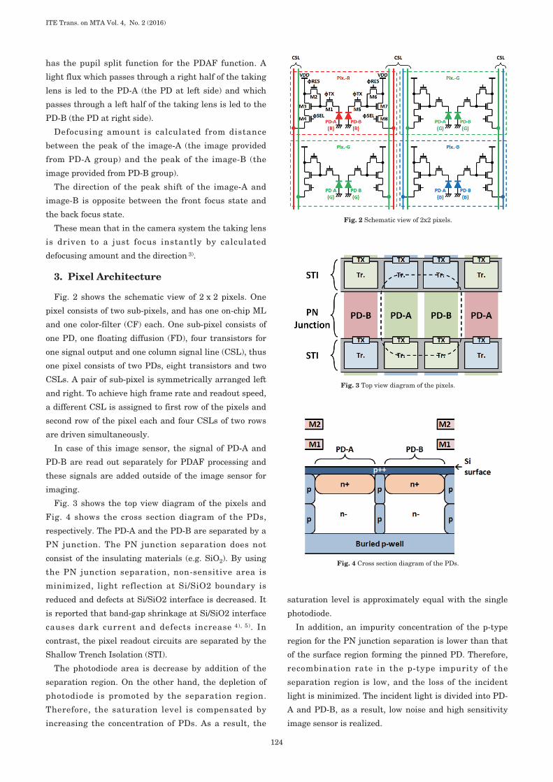
Fig. 2 shows the schematic view of 2 x 2 pixels. One
pixel consists of two sub-pixels, and has one on-chip ML
and one color-filter (CF) each. One sub-pixel consists of
one PD, one floating diffusion (FD), four transistors for
one signal output and one column signal line (CSL), thus
one pixel consists of two PDs, eight transistors and two
CSLs. A pair of sub-pixel is symmetrically arranged left
and right. To achieve high frame rate and readout speed,
a different CSL is assigned to first row of the pixels and
second row of the pixel each and four CSLs of two rows
are driven simultaneously.
In case of this image sensor, the signal of PD-A and
PD-B are read out separately for PDAF processing and
these signals are added outside of the image sensor for
imaging.
Fig. 3 shows the top view diagram of the pixels and
Fig. 4 shows the cross section diagram of the PDs,
respectively. The PD-A and the PD-B are separated by a
PN junction. The PN junction separation does not
consist of the insulating materials (e.g. SiO2). By using
the PN junction separation, non-sensitive area is
minimized, light reflection at Si/SiO2 boundary is
reduced and defects at Si/SiO2 interface is decreased. It
is reported that band-gap shrinkage at Si/SiO2 interface
causes dark current and defects increase 4), 5). In
contrast, the pixel readout circuits are separated by the
Shallow Trench Isolation (STI).
The photodiode area is decrease by addition of the
separation region. On the other hand, the depletion of
photodiode is promoted by the separation region.
Therefore, the saturation level is compensated by
increasing the concentration of PDs. As a result, the
saturation level is approximately equal with the single
photodiode.
In addition, an impurity concentration of the p-type
region for the PN junction separation is lower than that
of the surface region forming the pinned PD. Therefore,
recombination rate in the p-type impurity of the
separation region is low, and the loss of the incident
light is minimized. The incident light is divided into PD-
A and PD-B, as a result, low noise and high sensitivity
image sensor is realized.
ITE Trans. on MTA Vol. 4, No. 2 (2016)
124
Fig. 4 Cross section diagram of the PDs.
Fig. 2 Schematic view of 2x2 pixels.
Fig. 3 Top view diagram of the pixels.
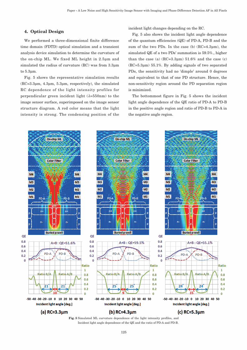
4. Optical Design
We performed a three-dimensional finite difference
time domain (FDTD) optical simulation and a transient
analysis device simulation to determine the curvature of
the on-chip ML. We fixed ML height in 2.5µm and
simulated the radius of curvature (RC) was from 3.3µm
to 5.3µm.
Fig. 5 shows the representative simulation results
(RC=3.3µm, 4.3µm, 5.3µm, respectively), the simulated
RC dependence of the light intensity profiles for
perpendicular green incident light (λ=550nm) to the
image sensor surface, superimposed on the image sensor
structure diagram. A red color means that the light
intensity is strong. The condensing position of the
incident light changes depending on the RC.
Fig. 5 also shows the incident light angle dependence
of the quantum efficiencies (QE) of PD-A, PD-B and the
sum of the two PDs. In the case (b) (RC=4.3µm), the
simulated QE of a two PDs' summation is 59.5%., higher
than the case (a) (RC=3.3µm) 51.6% and the case (c)
(RC=5.3µm) 55.1%. By adding signals of two separated
PDs, the sensitivity had no 'dimple' around 0 degrees
and equivalent to that of one PD structure. Hence, the
non-sensitivity region around the PD separation region
is minimized.
The bottommost figure in Fig. 5 shows the incident
light angle dependence of the QE ratio of PD-A to PD-B
in the positive angle region and ratio of PD-B to PD-A in
the negative angle region.
125
Paper » A Low Noise and High Sensitivity Image Sensor with Imaging and Phase-Difference Detection AF in All Pixels
Fig. 5 Simulated ML curvature dependence of the light intensity profiles, and
Incident light angle dependence of the QE and the ratio of PD-A and PD-B.
The angle range below the ratio of 0.2 is compared in
three cases. In the case (b), the angle range is 25
degrees. The range is wider than the case (a) 21 degrees
and the case (c) 24 degrees. The wider range means the
image-A and the image-B can be separated at wider
range of the incident light angle, and the AF
performance is improved.
Similarly, the angle range above the ratio of 0.2 near 0
degrees is compared. In the case (b), the angle range is 9
degrees. The range is narrower than the case of (a) 10
degrees and the case of (c) 15 degrees. The narrower
range near 0 degrees means the separation of image-A
and the image-B is better at larger F-number (=smaller
aperture) (Fig. 6).
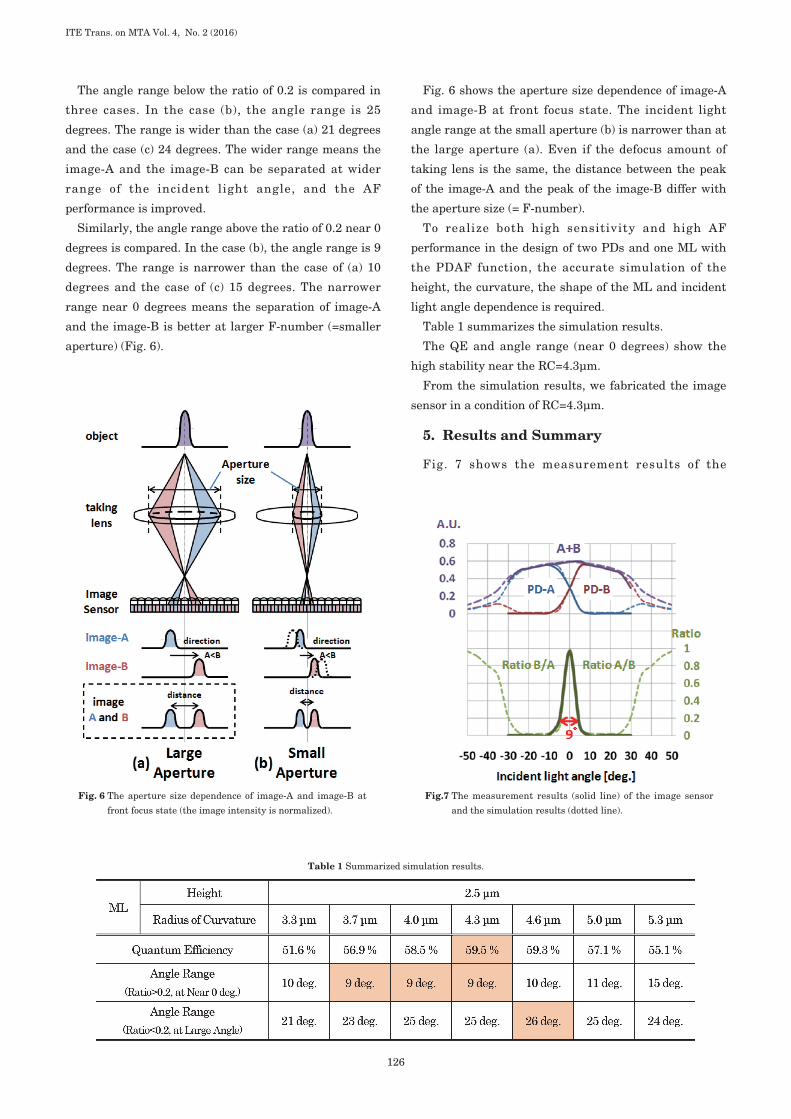
Fig. 6 shows the aperture size dependence of image-A
and image-B at front focus state. The incident light
angle range at the small aperture (b) is narrower than at
the large aperture (a). Even if the defocus amount of
taking lens is the same, the distance between the peak
of the image-A and the peak of the image-B differ with
the aperture size (= F-number).
To realize both high sensitivity and high AF
performance in the design of two PDs and one ML with
the PDAF function, the accurate simulation of the
height, the curvature, the shape of the ML and incident
light angle dependence is required.
Table 1 summarizes the simulation results.
The QE and angle range (near 0 degrees) show the
high stability near the RC=4.3µm.
From the simulation results, we fabricated the image
sensor in a condition of RC=4.3µm.
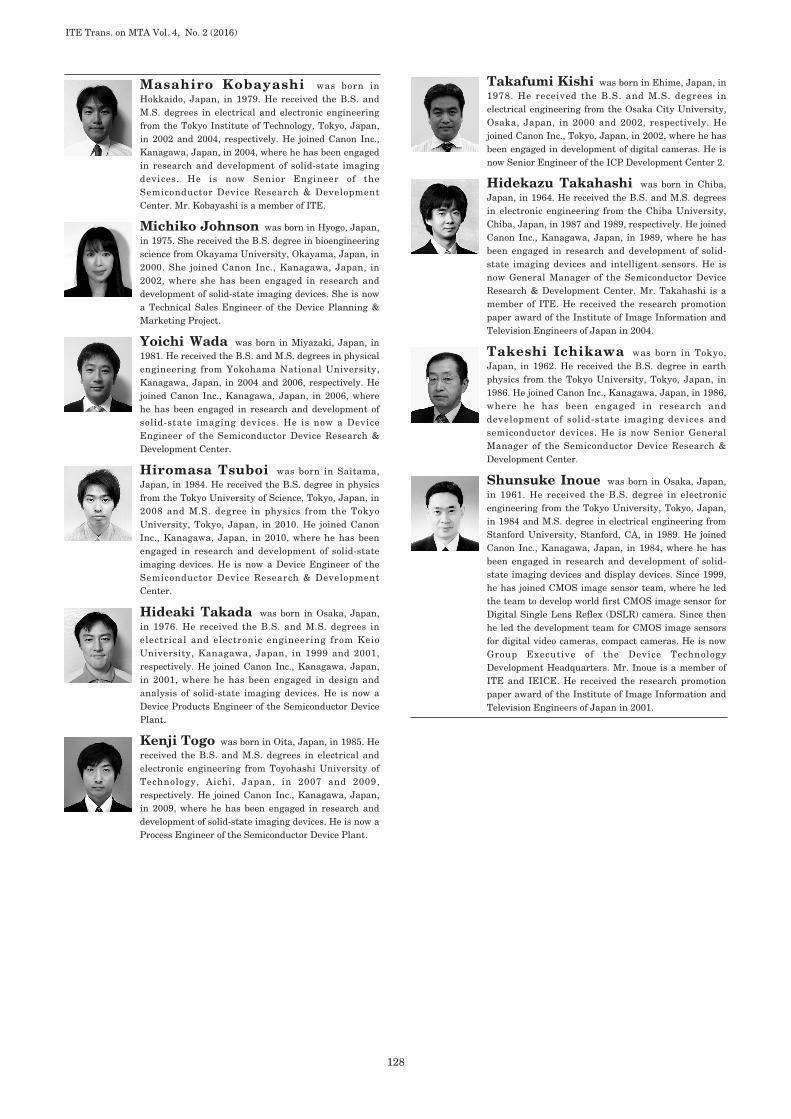
5. Results and Summary
Fig. 7 shows the measurement results of the
ITE Trans. on MTA Vol. 4, No. 2 (2016)
126
Fig.7 The measurement results (solid line) of the image sensor
and the simulation results (dotted line).
Table 1 Summarized simulation results.
Fig. 6 The aperture size dependence of image-A and image-B at
front focus state (the image intensity is normalized).

127
Paper » A Low Noise and High Sensitivity Image Sensor with Imaging and Phase-Difference Detection AF in All Pixels
fabricated image sensor. The solid line shows
measurement results and the dotted line shows
simulation results, and the vertical axis is normalized.
The both results are approximately equal, and the angle
range above the ratio of 0.2 near 0 degrees is about 9
degrees.
Table 2 summarizes the specifications and the
performances of this image sensor. Fabrication process
is 0.18µm 1Poly 4Metal CMOS process. Optical format is
super 35mm. Pixel size is 6.4 µm x 6.4 µm. Number of
effective pixels and the PDAF points are both 9.2M.
Number of effective PDs is 18.5M. Full well capacity is
40Ke- (@one pixel = two PDs). Sensitivity is 78Ke-/lx.s
(@2,856K light source with IR-cut-filter, one green
pixel). Dark random noise is 1.8e- at one PD and 2.5e- at
one pixel (@gain=32, RT). Dark current is 50e- at one
pixel (@60C, one second). Maximum frame rate is
60frames per second with full pixel readout.
The effective AF area is 80% (H) x 80% (V) of effective
pixels to guarantee accuracy of PDAF. AF speed is 4
times faster than conventional contrast AF.
Fig. 8 shows the photograph of packaged image
sensor. Chip size is 29.9mm (H) x 21.6mm (V).
High grade and high speed imaging has been achieved
by the low noise and high sensitivity image sensor with
imaging and phase-difference detection AF in all
effective pixels.
6. Acknowledgement
The authors would like to thank Kazunari Kawabata,
Taro Kato, Junji Iwata, Yu Arishima, Akira Okita,
Akiharu Takabayashi, Ichiro Onuki and Yoshihito
Harada the member of Canon Inc. for their contribution
to this work.
References
1) S. Uchiyama: "Superiority of Image Plane Phase Detection AF",ITE Technical Report, 36.38, pp.17 (2012)
2) H. Endo: ""Phase Detection Pixel Built-in Image Sensor" to RealizeHigh Speed Auto Focus", The journal of the Institute of ImageInformation and Television Engineers, 65.3, pp.290-292 (2011)
3) I. Onuki: "Digital Camera with Phase Detection Image Sensor",The journal of the Institute of Image Information and TelevisionEngineers, 68.3, pp.203-207 (2014)
4) K. Takeuchi, et al., "Si band-gap shrinkage caused by local strainat Si/SiO2 edge", Applied physics letters, 61.21, pp.2566-2568(1992)
5) K. Itonaga, et al., "Extremely-Low-Noise CMOS Image Sensor withHigh Saturation Capacity", Electron Devices Meeting (IEDM), 2011IEEE International. IEEE, 8.1.1 - 8.1.4 (2011)
Fig.8 The photograph of packaged image sensor.
Table 2 Summarized specifications and performances of this
image sensor.
ITE Trans. on MTA Vol. 4, No. 2 (2016)
128
Hiromasa Tsuboi was born in Saitama,Japan, in 1984. He received the B.S. degree in physicsfrom the Tokyo University of Science, Tokyo, Japan, in2008 and M.S. degree in physics from the TokyoUniversity, Tokyo, Japan, in 2010. He joined CanonInc., Kanagawa, Japan, in 2010, where he has beenengaged in research and development of solid-stateimaging devices. He is now a Device Engineer of theSemiconductor Device Research & DevelopmentCenter.
Hideaki Takada was born in Osaka, Japan,in 1976. He received the B.S. and M.S. degrees inelectrical and electronic engineering from KeioUniversity, Kanagawa, Japan, in 1999 and 2001,respectively. He joined Canon Inc., Kanagawa, Japan,in 2001, where he has been engaged in design andanalysis of solid-state imaging devices. He is now aDevice Products Engineer of the Semiconductor DevicePlant.
Kenji Togo was born in Oita, Japan, in 1985. Hereceived the B.S. and M.S. degrees in electrical andelectronic engineering from Toyohashi University ofTechnology, Aichi, Japan, in 2007 and 2009,respectively. He joined Canon Inc., Kanagawa, Japan,in 2009, where he has been engaged in research anddevelopment of solid-state imaging devices. He is now aProcess Engineer of the Semiconductor Device Plant.
Yoichi Wada was born in Miyazaki, Japan, in1981. He received the B.S. and M.S. degrees in physicalengineering from Yokohama National University,Kanagawa, Japan, in 2004 and 2006, respectively. Hejoined Canon Inc., Kanagawa, Japan, in 2006, wherehe has been engaged in research and development ofsolid-state imaging devices. He is now a DeviceEngineer of the Semiconductor Device Research &Development Center.
Michiko Johnson was born in Hyogo, Japan,in 1975. She received the B.S. degree in bioengineeringscience from Okayama University, Okayama, Japan, in2000. She joined Canon Inc., Kanagawa, Japan, in2002, where she has been engaged in research anddevelopment of solid-state imaging devices. She is nowa Technical Sales Engineer of the Device Planning &Marketing Project.
Masahiro Kobayashi was born inHokkaido, Japan, in 1979. He received the B.S. andM.S. degrees in electrical and electronic engineeringfrom the Tokyo Institute of Technology, Tokyo, Japan,in 2002 and 2004, respectively. He joined Canon Inc.,Kanagawa, Japan, in 2004, where he has been engagedin research and development of solid-state imagingdevices. He is now Senior Engineer of theSemiconductor Device Research & DevelopmentCenter. Mr. Kobayashi is a member of ITE.
Shunsuke Inoue was born in Osaka, Japan,in 1961. He received the B.S. degree in electronicengineering from the Tokyo University, Tokyo, Japan,in 1984 and M.S. degree in electrical engineering fromStanford University, Stanford, CA, in 1989. He joinedCanon Inc., Kanagawa, Japan, in 1984, where he hasbeen engaged in research and development of solid-state imaging devices and display devices. Since 1999,he has joined CMOS image sensor team, where he ledthe team to develop world first CMOS image sensor forDigital Single Lens Reflex (DSLR) camera. Since thenhe led the development team for CMOS image sensorsfor digital video cameras, compact cameras. He is nowGroup Executive of the Device TechnologyDevelopment Headquarters. Mr. Inoue is a member ofITE and IEICE. He received the research promotionpaper award of the Institute of Image Information andTelevision Engineers of Japan in 2001.
Takeshi Ichikawa was born in Tokyo,Japan, in 1962. He received the B.S. degree in earthphysics from the Tokyo University, Tokyo, Japan, in1986. He joined Canon Inc., Kanagawa, Japan, in 1986,where he has been engaged in research anddevelopment of solid-state imaging devices andsemiconductor devices. He is now Senior GeneralManager of the Semiconductor Device Research &Development Center.
Hidekazu Takahashi was born in Chiba,Japan, in 1964. He received the B.S. and M.S. degreesin electronic engineering from the Chiba University,Chiba, Japan, in 1987 and 1989, respectively. He joinedCanon Inc., Kanagawa, Japan, in 1989, where he hasbeen engaged in research and development of solid-state imaging devices and intelligent sensors. He isnow General Manager of the Semiconductor DeviceResearch & Development Center. Mr. Takahashi is amember of ITE. He received the research promotionpaper award of the Institute of Image Information andTelevision Engineers of Japan in 2004.
Takafumi Kishi was born in Ehime, Japan, in1978. He received the B.S. and M.S. degrees inelectrical engineering from the Osaka City University,Osaka, Japan, in 2000 and 2002, respectively. Hejoined Canon Inc., Tokyo, Japan, in 2002, where he hasbeen engaged in development of digital cameras. He isnow Senior Engineer of the ICP Development Center 2.