Embed Size (px)
Citation preview

816 JOURNAL OF MICROELECTROMECHANICAL SYSTEMS, VOL. 19, NO. 4, AUGUST 2010
A High-Power Temperature-Stable Electrostatic RFMEMS Capacitive Switch Based on a Thermal
Buckle-Beam DesignRashed Mahameed, Member, IEEE, Member, ASME, and Gabriel M. Rebeiz, Fellow, IEEE
Abstract—This paper presents the design, fabrication and mea-surements of a novel vertical electrostatic RF MEMS switch whichutilizes the lateral thermal buckle-beam actuator design in orderto reduce the switch sensitivity to thermal stresses. The effect ofbiaxial and stress gradients are taken into consideration, and thebuckle-beam designs show minimal sensitivity to these stresses.Several switches with 4, 8, and 12 suspension beams are presented.All the switches demonstrate a low sensitivity to temperature,and the variation in the pull-in voltage is ∼ −50 mV/◦C from25–125 ◦C. The change in the up-state capacitance for the sametemperature range is < ±3%. The switches also exhibit excellentRF and mechanical performances, and a capacitance ratio of∼20–23 (Cu = 85–115 fF, Cd = 1.7–2.6 pF) with Q > 150at 10 GHz in the up-state position is reported. The mechanicalresonant frequencies and quality factors are fo = 60–160 kHzand Qm = 2.3–4.5, respectively. The measured switching andrelease times are ∼2−5 μs and ∼5–6.5 μs, respectively. Powerhandling measurements show good stability with ∼4 W of incidentpower at 10 GHz. [2009-0319]
Index Terms—Microactuators, RF MEMS, switches, tempera-ture sensitivity.
I. INTRODUCTION
COMPARED to conventional solid-state switches,RF MEMS switches exhibit low loss, high linearity, and
very low power consumption [1]. However, some devices,particularly those with clamped–clamped and multilayer struc-tures, suffer from temperature effects due to their mechanicaldesign. This sensitivity is represented by a change in thepull-in voltage and the up-state capacitance due to the air-gapchange. Also, clamped–clamped switches with thin suspendedmembranes suffer from a spring constant variation as they areexposed to a temperature change. This is due to the reactionforces from the anchors and results in a reduction of the overallresidual tensile stress in the thin-film structure [1], [2].
In recent years, several RF MEMS capacitive switch designshave been demonstrated with low temperature sensitivity [3]–[14]. This was achieved using thin multilayer structures [3]–[5], optimized actuator design [6], [7], cantilever-based designs
Manuscript received December 15, 2009; revised April 12, 2010; acceptedApril 23, 2010. Date of publication June 1, 2010; date of current versionJuly 30, 2010. This work was supported by the Defense Advanced ResearchProjects Agency Center on RF MEMS Reliability and Design Fundamentals,with Dr. Dennis Polla as the Program Manager. Subject Editor G. Stemme.
The authors are with the Electrical and Computer Engineering Department,University of California at San Diego, La Jolla, CA 92093 USA (e-mail:[email protected]; [email protected]; [email protected]).
Color versions of one or more of the figures in this paper are available onlineat http://ieeexplore.ieee.org.
Digital Object Identifier 10.1109/JMEMS.2010.2049475
[8], [9], low-k springs to absorb the membrane expansion [10],[11], and molybdenum for the membrane material [12]. Also,miniature MEMS switches have been shown to result in lowtemperature sensitivity [13], [14]. All of these solutions requireeither advanced MEMS design efforts or special materials, anda precise fabrication flow.
In this paper, we present an electrostatic MEMS switchwith a new and robust temperature compensation mechanism.The design is based on a Chevron thermal actuator that hasbeen used for in-plane displacement and force applicationsin mechanical actuators [15]–[17]. The electrostatic actuatormoves vertically, but the thermal stress compensation mecha-nism results in a lateral movement rather than vertical bendingor buckling. The new design is simple to implement, requiresvirtually no design optimization, and can be fabricated usingstandard gold electroplating. Also, the design is highly tolerantto large amounts of biaxial-stress and stress gradients andcan therefore be built using nickel or copper electroplatingtechniques. The design can also handle a large amount ofRF power without suffering from adverse heating effects.
II. PRINCIPLE OF OPERATION
Fig. 1 shows a schematic view of the mechanical part of theMEMS switch, which is based on a Chevron thermal actuator[15]–[17]. The switch is vertically actuated; however, the ther-mal compensation mechanism results in a lateral movement.In this design, a suspended plate is connected by N beamsto two rigid anchors. Each beam width (wb) is smaller thanthe beam thickness (t), and the beam axis is tilted by angleα from the y-axis. This results in a large stiffness differencein the x- and z-axes, i.e., kz � kx. When the device is heatedup or cooled down, the thermal expansion/contraction of thestructure is translated to an in-plane displacement (δTx), andthe internal thermal stresses are released. Therefore, the platedoes not move vertically (δTz ≈ 0) and maintains a constantpull-in voltage (Vp) versus temperature.
The proposed device is not completely identical to the typicalChevron thermal actuator. The MEMS switch is not perfectlyplanar and includes vertical topography due to the bottom elec-trode underneath the suspended plate. This topography inducesinternal bending moments and results in a vertical displacementdue to a temperature change [18]. The device is thereforesimulated in CoventorWare [19] to evaluate the exact verticaland horizontal displacements due to temperature change.
1057-7157/$26.00 © 2010 IEEE

MAHAMEED AND REBEIZ: RF MEMS CAPACITIVE SWITCH BASED ON A THERMAL BUCKLE-BEAM DESIGN 817
Fig. 1. Schematic view of the mechanical part of the MEMS switch (a CPWline is also present for RF measurements—not shown).
A. Temperature Effect With no Stress
The beam width should be smaller than its thickness in orderto translate the thermal expansion to in-plane displacements.However, using thin films for the structure thickness (∼1 μm),which is the typical thickness in many capacitive RF MEMSswitches, results in a thickness-to-width ratio that is impracticalto fabricate. Therefore, it is imperative to use a thick layer (t >3 μm) so as to define the switch using standard lithographictechniques.
Fig. 2 shows the simulated vertical displacement of a12-beam device due to a temperature change ΔT = 100 ◦C.The simulations are done for a gold switch with E = 45 GPa,thermal expansion coefficient α∗ = 14 · 10−6 (1/◦C), L =75 μm, w = 150 μm, Lb = 90 μm, and p = 23 μm (Fig. 1).In these simulations, the thickness of the bottom electrode thatforms the topography is ta = 0.45 μm. The biaxial-stress andvertical-stress gradients are assumed to be zero. The simulatedvertical displacement with untilted beams (α = 0◦) is muchlarger than α = 5◦ and 10◦ for all wb/t values. This stronglyaffects the device performance, particularly when the switchair gap is ∼1 μm. The tilted beams also reduce the verticaldisplacement even when wb/t = 1. Note that the tilted beamsresult in larger displacements in the x-direction (Fig. 3), but thisis immaterial for a switch design.
A larger α results in a smaller vertical displacement [Fig. 2(a)versus 2(b)]; however, the structure stiffness becomes nonuni-form along the plate, and the plate profile becomes unsym-metrical around the plate center. The plate profile of the
Fig. 2. Simulated vertical displacement (δTz) of the switch for ΔT =100 ◦C versus thickness with (a) α = 5◦ and (b) α = 10◦.
Fig. 3. Simulated horizontal displacement (δTx) of the switch for ΔT =100 ◦C versus thickness at α = 0◦ and α = 10◦.
12-beam device with different α, ΔT = 100 ◦C, t = 7 μm, andwb = 3 μm is shown in Fig. 4. It is seen that the device with asmall α shows the flattest plate profile.
The effect of the topography on the switch vertical deflectionis shown in Fig. 5. It is shown that increasing the bottom-electrode thickness (ta) increases the vertical deflection of thesuspended plate due to the bending moments produced at thestep. However, the tilted beam design with α = 10◦ signifi-cantly reduces this deflection due to the in-plane displacementeffect.
B. Biaxial-Stress and Stress-Gradient Effects
The sensitivity of the new design to residual stresses isalso investigated. For this purpose, the device is simulated

818 JOURNAL OF MICROELECTROMECHANICAL SYSTEMS, VOL. 19, NO. 4, AUGUST 2010
Fig. 4. Plate profile when the beam tilted angle is 0◦−30◦ for ΔT =100 ◦C (wb = 3 μm, t = 7 μm).
Fig. 5. Simulated vertical displacement (δTz) versus bottom-electrode thick-ness (ta) of a 12-beam switch with topography for ΔT = 100 ◦C and α = 0◦,α = 10◦.
with internal in-plane stress (σ) and stress gradient (∇σ). Themechanical stiffness of the clamped–clamped structure is givenby [1]
kz = k1 + k2 (1)
where k1 is the structural stiffness, which is determined fromthe Young’s modulus and device geometry, and k2 is the stiff-ness due to the biaxial residual stress. For a clamped–clampedstructure, a temperature change will change k2 and the pull-in voltage of the device [1]. Fig. 6 shows the stiffness ratio(k2/k1) of a 12-beam device versus in-plane stress. The devicehas the same dimensions above with wb = 3 μm. A devicewith α = 10◦ has a much lower k2/k1 than that with α = 0◦
[Fig. 6(a) and (b)], and k2/k1 is also irrelative to σ. Thegeometrical constraint wb/t < 1 that occurs for wb = 3 μm andt = 7 μm also significantly reduces the device sensitivity to in-plane stress, particularly for α → 0◦. For σ = 100 MPa, k2/k1
drops from ∼200% (t = 3 μm) to ∼40% (t = 7 μm). A tensilestress in the device induces an in-plane displacement in the−x-direction [Fig. 6(c)], and the α = 10◦ device has a higherstiffness in the x-direction compared to the α = 5◦ device andresults in a smaller δσx. As mentioned before, this displacementis irrelevant from an RF MEMS switch perspective. The plateprofile at σ = 100 MPa is shown in Fig. 6(d), and the verticaldisplacement with α = 0◦ is insignificant due to its high springconstant (kz = 800 N/m). For α = 5◦ and 10◦, the deflection
Fig. 6. Simulated 12-beam device, stiffness for (a) t = 3 μm and (b) t =7 μm, and (c) in-plane displacement (δσx) for t = 7 μm versus in-plane stress.(d) Plate profile of a 12-beam device with t = 7 μm and σ = 100 MPa.
is < 0.1 μm at the center of the plate and should not have anadverse effect on the switch up-state capacitance.
Fig. 7(a) shows the maximum vertical displacement of a12-beam device versus stress gradient with an average in-planestress of 50 MPa. A thick device (t = 7 μm) greatly reduces thez-deflection at high stress gradient values. A t = 7-μm devicewith a stress gradient ∇σ = 4 MPa/μm (which is relativelyconsidered high in thick MEMS structures) has a maximumdeflection < 0.2 μm [Fig. 7(b)].
To demonstrate the robustness of the new device tothermal and residual stresses, a 12-beam device with σ =50 MPa, σ = 100 MPa, and ∇σ = 4 MPa/μm is simulated for

MAHAMEED AND REBEIZ: RF MEMS CAPACITIVE SWITCH BASED ON A THERMAL BUCKLE-BEAM DESIGN 819
Fig. 7. (a) Simulated maximum vertical displacement of a 12-beam devicewith average in-plane stress σ = 50 MPa versus stress gradient (∇σ). (b) Plateprofile of a 12-beam device with stress gradient of 4 MPa/μm and average in-plane stress of 50 MPa.
TABLE ISIMULATED DISPLACEMENTS OF A 12-BEAM DEVICE WITH STRESS
GRADIENT ∇σ = 4 MPa/μm AND IN-PLANE STRESSES
OF 50 AND 100 MPa FOR ΔT = 100 ◦C
ΔT = 100 ◦C (Table I). The simulations show that δz <0.15 μm for t = 7 μm, σ = 100 MPa, and α = 5◦, 10◦. Thisshows that the novel switch has very low sensitivity to residualand thermal stresses under a large range of conditions.
III. FABRICATION
The switches are fabricated on a 500-μm-thick quartz sub-strate (Fig. 8). First, a bottom metal with 200 Å/3000 Å ofTi/Au is sputtered and patterned to form the bottom electrodeof the switch. Next, 1200–1500 Å of PECVD Si3N4 is patternedon top of the bottom electrode (Fig. 8). An ∼1.1-μm sacrificiallayer (PMMA) is spin coated and patterned using a Ti mask andreactive ion etching. A seed layer with 200 Å/3000 Å/200 Åof Ti/Au/Ti is then sputtered and used for the electroplat-ing of the thick gold layer. A thick photoresist (SPR-220) isused to define the beam structure and the coplanar waveguide(CPW) lines of the device. After the Au electroplating(∼7 μm) and wet etch of the seed layer, the sacrificial layer
Fig. 8. Process flow: (a) Au bottom metal. (b) Si3N4 as the dielectric layer.(c) PMMA sacrificial layer. (d) Gold electroplating. (e) CPD for releasing thestructures.
is removed using a Microposit remover 1165 at 50 ◦C, and thewafer is dried with CO2 in a critical-point dryer (CPD) system.Notice that the topography underneath the switch plate that isinduced due to the bottom electrode creates a nonplanarizeddevice with ∼4500-Å step height.
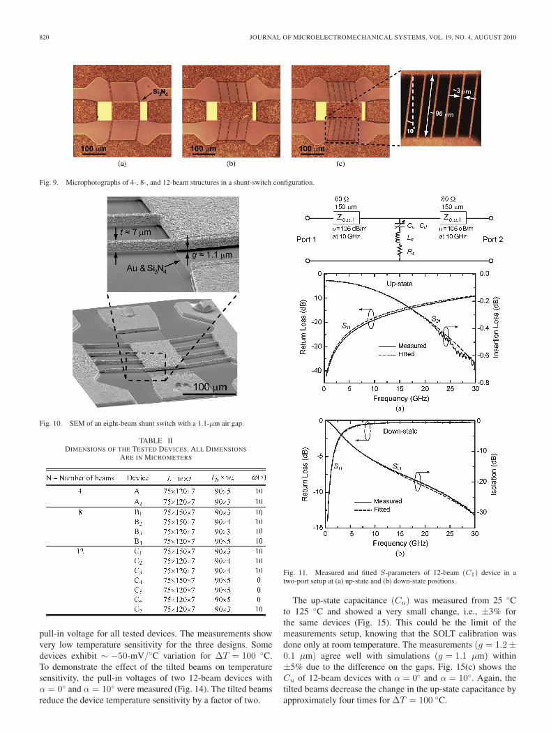
Fig. 9 shows microphotographs of three fabricated switcheswith 4, 8, and 12 beams. Fig. 10 shows an SEM photographof an eight-beam device with t ≈ 7 μm, wb ≈ 3 μm, and g ≈1.1 μm.
IV. MEASUREMENTS
In this section, the RF and mechanical performances of threeshunt switches with 4, 8, and 12 beams are presented. Table IIsummarizes the dimensions of the tested devices.
A. RF Measurements
The RF performance was measured on-wafer using anAgilent network analyzer, CPW probes, and short-open-load-through (SOLT) calibration. Fig. 11 shows the measured andfitted S-parameters of a two-port 12-beam device (C1) andits equivalent model. Fig. 12 shows the measured and fittedS-parameters of C1 in a one-port setup. The quality factor (Q)was obtained from the one-port S11 measurements (Fig. 12)using the formula Q = |Im(Z)|/Re(Z), where Z is the deviceimpedance, as extracted from S11 [1]. A quality factor > 150 at10 GHz is achieved in the up-state position with Cu = 115 fFfor C1. Table III summarizes the measured capacitance, Ls, Rs,and Q of three different devices. It is important to note that thefitted Cu, Ls, and Rs agree well with HFSS [20] simulations.The measured Cd is 1.74–2.69 pF and results in an εeff of3.3–3.9 for 1500 Å of silicon nitride dielectric (εr = 7). Thisreduction in εr is due to the roughness of the bottom metal anddielectric [1].
B. Temperature Measurements
Fig. 13 shows the measured and simulated pull-in and releasevoltages versus temperatures for several 4-, 8-, and 12-beamdevices. The devices were simulated with an average in-planestress σ = 40 MPa and a stress gradient ∇σ = 2 MPa/μm.This stress gradient is due to the tensile stress in the seed layerand was independently verified for this process. As seen, thereis good agreement between the measured and the simulated
820 JOURNAL OF MICROELECTROMECHANICAL SYSTEMS, VOL. 19, NO. 4, AUGUST 2010
Fig. 9. Microphotographs of 4-, 8-, and 12-beam structures in a shunt-switch configuration.
Fig. 10. SEM of an eight-beam shunt switch with a 1.1-μm air gap.
TABLE IIDIMENSIONS OF THE TESTED DEVICES. ALL DIMENSIONS
ARE IN MICROMETERS
pull-in voltage for all tested devices. The measurements showvery low temperature sensitivity for the three designs. Somedevices exhibit ∼ −50-mV/◦C variation for ΔT = 100 ◦C.To demonstrate the effect of the tilted beams on temperaturesensitivity, the pull-in voltages of two 12-beam devices withα = 0◦ and α = 10◦ were measured (Fig. 14). The tilted beamsreduce the device temperature sensitivity by a factor of two.
Fig. 11. Measured and fitted S-parameters of 12-beam (C1) device in atwo-port setup at (a) up-state and (b) down-state positions.
The up-state capacitance (Cu) was measured from 25 ◦Cto 125 ◦C and showed a very small change, i.e., ±3% forthe same devices (Fig. 15). This could be the limit of themeasurements setup, knowing that the SOLT calibration wasdone only at room temperature. The measurements (g = 1.2 ±0.1 μm) agree well with simulations (g = 1.1 μm) within±5% due to the difference on the gaps. Fig. 15(c) shows theCu of 12-beam devices with α = 0◦ and α = 10◦. Again, thetilted beams decrease the change in the up-state capacitance byapproximately four times for ΔT = 100 ◦C.

MAHAMEED AND REBEIZ: RF MEMS CAPACITIVE SWITCH BASED ON A THERMAL BUCKLE-BEAM DESIGN 821
Fig. 12. Measured and fitted S-parameters and Q in the up-state and down-state positions of the 12-beam device (C1) at 0.5–30 GHz.
TABLE IIICAPACITANCE AND Q OF THE TESTED DEVICES AT 25 ◦C.
THE Q IS MEASURED AT 10 GHz
The very small change in the up-state capacitance demon-strates that the variation in pull-in voltage is most likely dueto the change of the structure spring constant (kz) rather thana change in the air gap. The spring constant is affected by theinitial tensile stress of the seed layer (3000-Å sputtered gold),and decreasing the seed layer thickness or etching it completelywill further improve the pull-down voltage versus temperature.
The mechanical stiffness of the devices can be extractedusing the pull-in voltage formula for a parallel-plate structureand is given by [1]
Vp = g
√8kz
27Cu=
√8kzg2
27(εoA/g + Cf )(2)
where Cu is the up-state capacitance of the switch and includesthe fringing capacitance (Cf ) between the two plates. Thestiffness of the devices is extracted from the measured Vp
Fig. 13. Measured and simulated pull-in and release voltages versus temper-atures for (a) 4-beam (A1, A2), (b) 8-beam (B1, B2, B3), and (c) 12-beam(C1, C2, C3) devices.
Fig. 14. Measured pull-in and release voltages versus temperatures for a12-beam device with 0◦ and 10◦ tilted angles.

822 JOURNAL OF MICROELECTROMECHANICAL SYSTEMS, VOL. 19, NO. 4, AUGUST 2010
Fig. 15. Measured and simulated up-state capacitances (Cu’s) versus temper-atures for (a) 4-beam, (b) 8-beam, and (c) 12-beam devices with 0◦ and 10◦
tilted angles.
TABLE IVMEASURED AND SIMULATED PULL-IN VOLTAGES AND STIFFNESSES
and Cu and summarized in Table IV. The measured g for thefabricated devices is 1.2 ± 0.1 μm, depending on its location onthe wafer. Good agreement is seen with finite-element method(FEM) simulations. The wide variation in the extracted kz fromthe measured Vp is due to kz being dependent on g−3.
C. Switching Time and Resonant Frequency Measurements
Fig. 16 shows the test setup for the switching time andmechanical resonant frequency of the devices. The devices weretested in atmospheric conditions at room temperature. A squarebipolar actuation voltage with 35–45 V and 1 kHz is appliedto the switch. The input RF power level is +10 dBm RF at10 GHz, and the output RF power is detected and monitoredon the scope. As shown in Fig. 17(a), an up-to-down switchingtime of ts ≈ 2 μs was measured for a 12-beam device. With anactuation voltage Vs = 45 V, a pull-in voltage Vp = 35 V, anda resonant frequency fo = 160 kHz, the calculated switching
Fig. 16. Switching time and resonant frequency measurement setup.
Fig. 17. Measured (a) switching time (ts) (up to down), (b) release time (tr)(down to up), and (c) measured and fitted resonant frequency of a 12-beamdevice in air.
time using ts ∼= 3.67 Vp/2πfoVs is 2.8 μs [1]. A tr ≈ 5-μsrelease time, down to up, was also measured for the same deviceand includes the charging effects in the Si3N4 dielectric.
The resonant frequency of the devices was measured withthe intermodulation product technique [1]. In this technique,a biased sinusoidal actuation voltage is applied together withRF power. This actuation voltage induces a displacement

MAHAMEED AND REBEIZ: RF MEMS CAPACITIVE SWITCH BASED ON A THERMAL BUCKLE-BEAM DESIGN 823
TABLE VMEASURED SWITCHING TIME AND Qm OF THE SWITCH
change at ωm, which results in a capacitance change and avariation in the output-voltage phase. This phase change, inturn, produces two sidebands at ωRF ± ωm. Using a spectrumanalyzer, the amplitude of the two sidebands was measuredwhile sweeping the frequency of the actuation voltage (ωm).Fig. 17(b) shows the measured and the fitted frequency responseof a 12-beam device that was actuated with VDC = 10 V,VAC = 5 sin(ωmt), and 10-dBm RF power at 10 GHz. Themechanical resonant frequency of the device is fm = 160 kHzwith mechanical quality factor Qm = 4.5 and agree well withFEM simulations. Table V summarizes the switching timeand the mechanical quality factor of three different designs.As seen, the four-beam device has a larger switching timecompared to other devices due to the lower stiffness of thedevice.
V. POWER HANDLING
A. Thermal Analysis
The low temperature sensitivity of the switch also makes it anexcellent candidate for high-power application. A 12-beam de-vice was simulated in HFSS in order to evaluate the RF currentdistribution in the up-state position. The current density is veryhigh in the outer beams, and the current is 10–20× lower on themiddle beams [Fig. 18(a)]. A symmetrical boundary conditionwas used in the simulations, and therefore, the simulated resultsare presented in a half device. The dissipated power by theswitch (Pdis) can be calculated by [1], [24]
Pdis = Pi
(1 − |S11|2 − |S21|2
)(3)
where Pi is the incident power and L = 1 − |S11|2 − |S21|2 isthe power loss in the switch. The S-parameters of a 12-beamdevice were simulated for the following two cases in a closed-box environment (no radiation): 1) The device is lossless(σc → ∞), including the CPW lines, and this results in |S11| =0.1039 and |S21| = 0.9946 at 10 GHz and L1 ≈ 0, and 2) theCPW lines and the metal underneath the switch are lossless,but the switch bridge, i.e., the plate, and the narrow beamsare lossy with a conductivity of σc = 3 × 10⁷ S/m due to theroughness of the electroplated gold [21]. The simulations showthat |S11| = 0.0696 and |S21| = 0.9967 at 10 GHz and L2 =0.0018. Accordingly, the dissipated power in the switch bridge,which converts to heat, is Pdis = PiL2. The same conditionsare assumed in the down-state position, and the simulationsshow that the dissipated power in the switch bridge is 0.0038Pi.
Based on the current density simulations, a thermal analysisof the device is performed using ePhysics software [22]. Thecurrent density solution of the device was exported to ePhysics,
Fig. 18. Simulated (a) current density distribution, (b) temperature distribu-tion for a dissipated power of ∼10 mW on the switch, and (c) maximum platetemperature of a 12-beam device in the up-state position versus incident power.
and the thermal steady-state analysis of the device was sim-ulated. In these simulations, the dissipated heat to the quartzsubstrate and its heat convection are considered. The gold-based switch has a thermal conductivity of kt = 297 W/mK,a density ρ = 19 300 kg/m3, a heat capacity C = 129 J/kg · K,and the same mechanical properties in Section II. The quartzproperties are as follows: kt = 1.4 W/mK, ρ = 2500 kg/m3,and C = 750 J/kgK. Also, the quartz substrate was taken to befive times larger than the device area, and the bottom and sidesurfaces of the quartz substrate are fixed at room temperature(25 ◦C). Fig. 18(b) shows the temperature distribution for a12-beam device in the up-state position, which is subjected toPi = 5 W (Pdis = 10 mW) and with a maximum temperatureof 82 ◦C. In this simulation, the switch plate temperature isshown to be 75 ◦C.
Fig. 19 shows the simulated current distribution and thetemperature field of the 12-beam device in the down-state

824 JOURNAL OF MICROELECTROMECHANICAL SYSTEMS, VOL. 19, NO. 4, AUGUST 2010
Fig. 19. Simulated (a) current density distribution, (b) temperature distribu-tion for a dissipated power of ∼10 mW on the switch, and (c) maximum platetemperature of a 12-beam device in the down-state position versus incidentpower.
position. In these simulations, a Si3N4 dielectric layer withkt = 1.8 W/mK, ρ = 2400 kg/m3, and C = 691 J/kgK is usedbetween the switch plate and the signal line.
The plate temperatures as a function of incident power inthe up- and down-state positions are shown in Figs. 18(c) and19(c), respectively. As seen, the temperature in the down-stateposition is higher than that in the up-state position [23]. Also,it is shown that using a thick metal reduces the developedtemperature in the switch. Due to the low temperature sen-sitivity of the 7-μm device at 25 ◦C–125 ◦C, the switch isexpected to handle an incident power of ∼10 W with a smallchange in the pull-in voltage. Furthermore, since the maximumtemperature is present only at the outer beams and the innerbeams are at a lower temperature, the simulated displacement
Fig. 20. Power-handling test setup.
Fig. 21. Measured Vp and Vr versus incident power of (a) 8-beam (B4) and(b) 12-beam (C7) devices.
in the center (δTz < 0.08 μm at T = 131 ◦C) is much lowerthan that simulated for a uniform temperature distribution, asshown in Section II.
B. Power-Handling Measurements
Fig. 20 shows the schematic test setup for the power-handling measurement. The cable losses were calibratedout in the measurements. The switch was actuated usinga triangular waveform. Fig. 21 shows the measured pull-in

MAHAMEED AND REBEIZ: RF MEMS CAPACITIVE SWITCH BASED ON A THERMAL BUCKLE-BEAM DESIGN 825
and release voltages of 8- and 12-beam devices as a functionof incident power (see Table I for dimensions). The 8- and12-beam devices were tested up to ∼3.25 and ∼4.4 W, respec-tively, and stuck down at higher power levels. The eight-beamdevice demonstrates a very small change in the pull-in voltageup to ∼2.75 W. The pull-in voltage in the 12-beam is reducedby ∼40% at ∼4.4 W. The equivalent Vrms on the device at4.4 W is Vrms = 14.8 V and has the effect of reducing Vp from43 V to V ′
p = 40.3 V (432 = V ′2p + V 2
rms). The additional Vp
drop to ∼25 is most likely due to the dielectric charging underhigh RF power levels or gold softening rather than the air-gapchange due to the temperature rise [24]–[26]. This effect iscurrently under investigation.
VI. CONCLUSION
A new temperature-stable electrostatic switch has beenpresented. The switch has very low temperature sensitivity∼ −50 mV/◦C at 25 ◦C–125 ◦C and has shown power handlingup to 4.4 W. The switch results in Cu = 85–115 fF and Cd =1.7–2.6 pF, which is suitable for microwave operation, and canbe scaled smaller for millimeter-wave operation. The designcan be cofabricated with metal-contact switches since both arebased on a thick-metal process (6–10 μm). Also, the design isvery insensitive to residual stress and to stress gradients, andthis allows the use of lower cost higher stress metal, such asnickel or copper, for membrane fabrication.
ACKNOWLEDGMENT
The authors would like to thank Dr. R. A. Alhalabi for hishelp in the electromagnetic simulations.
REFERENCES
[1] G. M. Rebeiz, RF MEMS Theory, Design and Technology. Hoboken, NJ:Wiley, 2003.
[2] C. L. Goldsmith and D. I. Forehand, “Temperature variation of actuationvoltage in capacitive MEMS switches,” IEEE Microw. Wireless Compon.Lett., vol. 15, no. 10, pp. 718–720, Oct. 2005.
[3] S. Duffy, C. Bozler, S. Rabe, J. Knecht, L. Travis, P. Wyatt, C. Keast,and M. Gouker, “MEMS microswitches for reconfigurable microwavecircuitry,” IEEE Microw. Wireless Compon. Lett., vol. 11, no. 3, pp. 106–108, Mar. 2001.
[4] J. Muldavin, C. Bozler, and C. Keast, “Wafer-scale packaged RF-MEMSswitches,” in IEEE MTT-S Int. Microw. Symp. Tech. Dig., San Francisco,CA, 2006, pp. 267–270.
[5] A. Stehle, C. Siegel, V. Ziegler, B. Schönlinner, U. Prechtel, S. Thilmont,H. Seidel, and U. Schmid, “Low complexity RF-MEMS switch optimizedfor operation up to 120 ◦C,” in Proc. Eur. Microw. Integr. Circuit Conf.,Munich, Germany, 2007, pp. 431–434.
[6] H. Nieminen, V. Ermolov, S. Silanto, K. Nybergh, and T. Ryhänen, “De-sign of a temperature-stable RF MEM capacitor,” J. Microelectromech.Syst., vol. 13, no. 5, pp. 705–714, Oct. 2004.
[7] I. Reines, B. Pillans, and G. M. Rebeiz, “A stress-tolerant temperature-stable RF MEMS switched capacitor,” in Proc. IEEE 22nd Int. Conf.Micro Electro Mech. Syst., Sorrento, Italy, 2009, pp. 880–883.
[8] R. Mahameed, N. Sinha, M. B. Pisani, and G. Piazza, “Dual-beam actu-ation of piezoelectric AlN RF MEMS switches monolithically integratedwith AlN contour-mode resonators,” J. Micromech. Microeng., vol. 18,no. 10, p. 105 011, Oct. 2008.
[9] A. Grichener, B. Lakshminarayanan, and G. M. Rebeiz, “High-Q RFMEMS capacitor with digital/analog tuning capabilities,” in IEEE MTT-SInt. Microw. Symp. Tech. Dig., Atlanta, GA, 2008, pp. 1283–1286.
[10] A. Morris, “Tunable RF modules for mobile applications,” in Proc. IEEEInt. Microw. Symp. Workshop Emerging Appl. RF-MEMS, Boston, MA,Jun. 2009.
[11] M. Reimann and M. Ulm, “RF MEMS and packaging strategies,” in Proc.IEEE Int. Microw. Symp. Workshop Adv. RF MEMS Packag. Technol.,Philadelphia, PA, Jun. 2003.
[12] C. Goldsmith, D. Forehand, D. Scarbrough, I. Johnston, S. Sampath,A. Datta, Z. Peng, C. Palego, and J. C. M. Hwang, “Perfor-mance of molybdenum as a mechanical membrane for RF MEMSswitches,” in IEEE MTT-S Int. Microw. Symp. Tech. Dig., Boston, MA,2009, pp. 1229–1232.
[13] V. Joshi, C. Smith, R. Gaddi, D. Lacey, T. Nagata, M. Renault,A. Unamuno, R. V. Kampen, R. Knipe, and D. Yost, “A non volatileMEMS switch for harsh environment memory applications,” in Proc. 10thAnnu. Non-Volatile Memory Technol. Symp., Portland, OR, 2009, p. 6-2.
[14] B. Lakshminarayanan, D. Mercier, and G. M. Rebeiz, “High-reliabilityminiature RF-MEMS switched capacitors,” IEEE Trans. Microw. TheoryTech., vol. 56, no. 4, pp. 971–981, Apr. 2008.
[15] L. Que, J.-S. Park, and Y. B. Gianchandani, “Bent-beam electro-thermalactuators for high force applications,” in Proc. IEEE Int. Conf. MicroElectro Mech. Syst., Orlando, FL, 1999, pp. 31–36.
[16] R. Cragun and L. L. Howell, “Linear thermomechanical microactua-tors,” in Proc. IMECE, ASME Int. Mech. Eng. Congr. Expo., Nov. 1999,pp. 181–188.
[17] C. D. Lott, T. W. McLain, J. N. Harb, and L. L. Howell, “Thermal mod-eling of a surface-micromachined linear-displacement thermomechanicalmicroactuator,” Sens. Actuators A, Phys., vol. 101, no. 1–2, pp. 239–250,Sep. 2002.
[18] J. Varona, M. Tecpoyotl-Torres, and A. A. Hamoui, “Design of MEMSvertical–horizontal Chevron thermal actuators,” Sens. Actuators A, Phys.,vol. 153, no. 1, pp. 127–130, Jun. 2009.
[19] Coventor, Inc., Cary, NC. [Online]. Available: www.coventor.com[20] Ansoft Corporation, High Frequency Structure Simulator (HFSS11).
[Online]. Available: www.ansoft.com/products/hf/hfss[21] J. C. Rautio, “An investigation of microstrip conductor loss,” IEEE Mi-
crow. Mag., vol. 1, no. 4, pp. 60–67, Dec. 2000.[22] Ansoft Corporation, ePhysics3.1. [Online]. Available: www.ansoft.com/
products/tools/ephysics/[23] F. Coccetti, B. Ducarouge, E. Scheid, D. Dubuc, K. Grenier, and R. Plana,
“Thermal analysis of RF-MEMS switches for power handling front-end,”in Proc. Eur. Microw. Conf., Paris, France, 2005, pp. 513–516.
[24] J. Rizk, E. Chaiban, and G. M. Rebeiz, “Steady state thermal analysis andhigh-power reliability considerations of RF MEMS capacitive switches,”in IEEE MTT-S Int. Microw. Symp. Tech. Dig., 2002, vol. 1, pp. 239–242.
[25] J. R. Reid, L. A. Starman, and R. T. Webster, “RF actuation of. capacitiveMEMS switches,” in IEEE MTT-S Int. Microw. Symp. Tech. Dig., 2003,pp. 1919–1922.
[26] J. Muldavin, R. Boisvert, C. Bozler, S. Rabe, and C. Keast, “Power han-dling and linearity of MEM capacitive series switches,” in IEEE MTT-SInt. Microw. Symp. Tech. Dig., 2003, pp. 1915–1918.
Rashed Mahameed (M’07) received the B.Sc.,M.Sc., and Ph.D. degrees from the Faculty of Me-chanical Engineering, Technion–Israel Institute ofTechnology, Haifa, Israel, in 2000, 2003, and 2006,respectively. His Ph.D. dissertation was on thermaleffects in microsystems (MEMS) and their applica-tion to novel microdevices.
From 2006 to 2008, he was a PostdoctoralResearcher at the University of Pennsylvania,Philadelphia. During that time, he developed the firstpiezoelectric aluminum nitride (AlN) RF MEMS
switch, which was cointegrated with AlN micromechanical contour-moderesonators and filters. He is currently an Assistant Project Scientist in theElectrical and Computer Engineering Department, University of Californiaat San Diego, La Jolla. His research interests are MEMS modeling; designand fabrication of thermoelastic, piezoelectric, and electrostatic actuators; andRF MEMS switches.
Dr. Mahameed is a member of the American Society of MechanicalEngineers (ASME).
826 JOURNAL OF MICROELECTROMECHANICAL SYSTEMS, VOL. 19, NO. 4, AUGUST 2010
Gabriel M. Rebeiz (F’97) received the Ph.D. de-gree from the California Institute of Technology,Pasadena.
From 1988 to 1996, he was involved in planarmillimeter-wave and terahertz antennas and imag-ing arrays. From 1988 to 2004, he was with theUniversity of Michigan, Ann Arbor. He is currentlya Professor of electrical and computer engineeringin the Electrical and Computer Engineering Depart-ment, University of California at San Diego (UCSD),La Jolla. He leads a group of 20 Ph.D. students
and five postdoctoral fellows at UCSD in the areas of millimeter-wave RFintegrated circuits (RFICs), microwave circuits, RF MEMS, planar millimeter-wave antennas, and terahertz systems. He is the Director of the UCSD/DefenseAdvanced Research Projects Agency Center on RF MEMS Reliability and De-sign Fundamentals. His group has optimized the dielectric-lens antenna, whichis the most widely used antenna at millimeter-wave and terahertz frequencies,and also developed 6–18- and 30–50-GHz 8- and 16-element phased arrayson a single silicon chip, making them one of the most complex RFICs atthis frequency range. His group also demonstrated high-Q RF MEMS tunablefilters at 1–6 GHz (Q > 200) and the new angular-based RF MEMS capacitiveand metal-contact switches. As a Consultant, he helped in the development ofthe USM/ViaSat 24-GHz single-chip automotive radar, several phased arraysoperating at X-, Ku-, and W-bands for defense and commercial applications,the RFMD RF MEMS switch, and the Agilent RF MEMS switch. He is theauthor of the book RF MEMS: Theory, Design, and Technology (Wiley, 2003).
Prof. Rebeiz is a National Science Foundation Presidential Young Inves-tigator and the IEEE Microwave Theory and Techniques (MTT) 2003 Dis-tinguished Young Engineer, and he is also the recipient of the IEEE MTT2000 Microwave Prize, the URSI Koga Gold Medal, and the IEEE MTT2010 Distinguished Educator Award. He also received the 1998 Eta-Kappa-NuProfessor of the Year Award and the 1998 Amoco Teaching Award given to thebest undergraduate teacher at the University of Michigan, and the 2008 Teacherof the Year Award at the Jacobs School of Engineering, UCSD. His studentshave won a total of 19 best paper awards at IEEE MTT, RFIC, and Antennasand Propagation Society (AP-S) conferences. He has been an Associate Editorof the IEEE MTT and a Distinguished Lecturer for IEEE MTT and the IEEEAntennas and Propagation Society.