Embed Size (px)
Citation preview

A Harmonic-Oscillator Design Method-ology Based on Describing Functions
Jesper Bank
Department of Signals and SystemsSchool of Electrical Engineeringchalmers university of technologySweden 2006


Thesis for the degree of Doctor of Philosophy
A Harmonic-Oscillator DesignMethodology Based on Describing
Functions
by
Jesper Bank
Department of Signals and SystemsCircuit Design Group
Chalmers University of TechnologySE-412 96 Goteborg, SwedenTelephone +46 (0)31 772 1000
Goteborg 2006

A Harmonic-Oscillator Design Methodology Based on Describing FunctionsJesper BankISBN 91-7291-748-2
This thesis has been prepared using LATEX.
Copyright c©2006, Jesper Bank.All rights reserved.
Doktorsavhandlingar vid Chalmers Tekniska HogskolaNy serie nr 2430ISSN 0346-718X
Department of Signals and SystemsCircuit Design GroupChalmers University of TechnologySE-412 96 Goteborg, SwedenTelephone +46 (0)31 772 1000
Front cover: Pendulum clock. Photograph by Erik Boman.
Printed in Sweden by Chalmers ReproserviceGoteborg, February 2006

Abstract
Oscillators are present in most electronic equipment where they provide tim-ing information, for example as sampling clocks in analog-to-digital convert-ers or as radio carriers in wireless communications. To design an oscillator,we must have knowledge of the properties and the operation of oscillators.Since oscillators are inherently nonlinear and are subject to noise, we have asystem that is difficult to analyze since the large wanted signal and the smallunwanted signal interact. It is shown in this thesis that describing func-tions can be used to calculate not only the large-signal behavior, but alsothe small-signal behavior using the method of impulse sensitivity functions.Based on theoretical results from this method, a design methodology forharmonic oscillators is derived and analyzed. The design methodology aimsat the design of harmonic oscillators fulfilling phase-noise requirements withminimized power consumption subject to constraints from the other require-ments set by the specification and the technology used to implement the os-cillator. The design methodology has been used to design oscillators meetingquite different specifications, both discrete and integrated implementationsand with either inductors and capacitors or crystals as frequency-determiningelements.
Keywords: oscillator, design methodology, describing function, impulsesensitivity function, frequency tuning, amplitude control, phase noise,oscillator design efficiency
i


Contents
Abstract i
Contents iii
Acknowledgements ix
Abbreviations and Acronyms xi
Notation xiii
1 Introduction 11.1 Background . . . . . . . . . . . . . . . . . . . . . . . . . . . . 1
1.1.1 Why do we need a Systematic Design Methodology? . 21.1.2 Analysis of Oscillators . . . . . . . . . . . . . . . . . . 31.1.3 Design of Oscillators . . . . . . . . . . . . . . . . . . . 3
1.2 Contributions . . . . . . . . . . . . . . . . . . . . . . . . . . . 41.3 Thesis Outline . . . . . . . . . . . . . . . . . . . . . . . . . . . 5
2 Oscillator Basics 72.1 Introduction . . . . . . . . . . . . . . . . . . . . . . . . . . . . 7
2.1.1 Feedback Model of an Oscillator . . . . . . . . . . . . . 92.2 Large-Signal Properties . . . . . . . . . . . . . . . . . . . . . . 10
2.2.1 Signal Waveform . . . . . . . . . . . . . . . . . . . . . 112.2.2 Frequency . . . . . . . . . . . . . . . . . . . . . . . . . 11
2.3 Small-Signal Properties . . . . . . . . . . . . . . . . . . . . . . 122.3.1 Amplitude Noise . . . . . . . . . . . . . . . . . . . . . 142.3.2 Phase Noise . . . . . . . . . . . . . . . . . . . . . . . . 142.3.3 Injection Locking . . . . . . . . . . . . . . . . . . . . . 16
2.4 Specifying an Oscillator . . . . . . . . . . . . . . . . . . . . . 16
iii

2.5 Designing an Oscillator . . . . . . . . . . . . . . . . . . . . . . 17
3 Oscillator Design Methodology 193.1 Introduction . . . . . . . . . . . . . . . . . . . . . . . . . . . . 193.2 Methodology . . . . . . . . . . . . . . . . . . . . . . . . . . . 20
3.2.1 First Step: Specification Attainable? . . . . . . . . . . 213.2.2 Second Step: Topology Selection . . . . . . . . . . . . 233.2.3 Third Step: Initial Component Sizing . . . . . . . . . . 243.2.4 Fourth Step: Simulation and Optimization . . . . . . . 263.2.5 Fifth Step: Implementation and Verification . . . . . . 26
3.3 Design Examples . . . . . . . . . . . . . . . . . . . . . . . . . 273.3.1 Crystal Oscillator . . . . . . . . . . . . . . . . . . . . . 273.3.2 VCO using JFET . . . . . . . . . . . . . . . . . . . . . 333.3.3 Integrated VCO using MOSFETs . . . . . . . . . . . . 41
3.4 Discussion . . . . . . . . . . . . . . . . . . . . . . . . . . . . . 50
4 Oscillator Topologies 514.1 Feedback Network . . . . . . . . . . . . . . . . . . . . . . . . . 51
4.1.1 Capacitors . . . . . . . . . . . . . . . . . . . . . . . . . 514.1.2 Inductors . . . . . . . . . . . . . . . . . . . . . . . . . 524.1.3 Varactors . . . . . . . . . . . . . . . . . . . . . . . . . 524.1.4 Crystals/Piezoelectric Resonators . . . . . . . . . . . . 534.1.5 Frequency-Determining Network . . . . . . . . . . . . . 554.1.6 LC Networks . . . . . . . . . . . . . . . . . . . . . . . 584.1.7 Crystal Networks . . . . . . . . . . . . . . . . . . . . . 624.1.8 Frequency Tuning . . . . . . . . . . . . . . . . . . . . . 63
4.2 Active Network . . . . . . . . . . . . . . . . . . . . . . . . . . 634.2.1 One-Transistor Networks . . . . . . . . . . . . . . . . . 644.2.2 Two-Transistor Networks . . . . . . . . . . . . . . . . . 654.2.3 Biasing . . . . . . . . . . . . . . . . . . . . . . . . . . . 65
4.3 Noise from Bias Current Source . . . . . . . . . . . . . . . . . 744.3.1 White Noise from Bias Current Source . . . . . . . . . 744.3.2 1/f Noise from Bias Current Source . . . . . . . . . . . 75
4.4 Phase-Noise Performance . . . . . . . . . . . . . . . . . . . . . 774.4.1 FET . . . . . . . . . . . . . . . . . . . . . . . . . . . . 774.4.2 BJT . . . . . . . . . . . . . . . . . . . . . . . . . . . . 844.4.3 Summary . . . . . . . . . . . . . . . . . . . . . . . . . 89
5 Amplitude Control 915.1 Introduction . . . . . . . . . . . . . . . . . . . . . . . . . . . . 915.2 Limiting Using Temperature-Sensitive Resistor . . . . . . . . . 92
iv

5.2.1 Phase-Noise Contribution . . . . . . . . . . . . . . . . 935.3 Diode Limiting . . . . . . . . . . . . . . . . . . . . . . . . . . 93
5.3.1 Phase-Noise Contribution . . . . . . . . . . . . . . . . 945.4 Limiting Using Nonlinearity in the Active Network . . . . . . 95
5.4.1 Phase-Noise Contribution . . . . . . . . . . . . . . . . 955.4.2 Differential Pair Current Source . . . . . . . . . . . . . 95
5.5 Automatic Amplitude Control . . . . . . . . . . . . . . . . . . 965.5.1 Amplitude Control Loop Stability . . . . . . . . . . . . 975.5.2 Transfer Function for the Feedback Network . . . . . . 975.5.3 Amplitude Detector . . . . . . . . . . . . . . . . . . . . 975.5.4 Control Amplifier . . . . . . . . . . . . . . . . . . . . . 995.5.5 Phase-Noise Contribution . . . . . . . . . . . . . . . . 99
5.6 Summary . . . . . . . . . . . . . . . . . . . . . . . . . . . . . 100
6 Frequency Tuning 1016.1 Introduction . . . . . . . . . . . . . . . . . . . . . . . . . . . . 1016.2 Large-Signal Capacitance . . . . . . . . . . . . . . . . . . . . . 1026.3 Frequency-Tuning Characteristics . . . . . . . . . . . . . . . . 1036.4 Phase Noise due to Frequency Tuning . . . . . . . . . . . . . . 1056.5 Diode Varactor . . . . . . . . . . . . . . . . . . . . . . . . . . 107
6.5.1 Background . . . . . . . . . . . . . . . . . . . . . . . . 1076.5.2 Phase-Noise Parameters . . . . . . . . . . . . . . . . . 108
6.6 MOS Varactor . . . . . . . . . . . . . . . . . . . . . . . . . . . 1136.6.1 Background . . . . . . . . . . . . . . . . . . . . . . . . 1136.6.2 Phase Noise Parameters . . . . . . . . . . . . . . . . . 113
6.7 Summary . . . . . . . . . . . . . . . . . . . . . . . . . . . . . 116
7 Phase-Noise Calculations 1177.1 Introduction . . . . . . . . . . . . . . . . . . . . . . . . . . . . 117
7.1.1 Assumptions . . . . . . . . . . . . . . . . . . . . . . . . 1187.2 Phase Noise due to White Noise . . . . . . . . . . . . . . . . . 118
7.2.1 Noise from Feedback Network . . . . . . . . . . . . . . 1187.2.2 Noise from Active Network . . . . . . . . . . . . . . . . 1207.2.3 Noise from Series Base and Gate Resistances . . . . . . 1217.2.4 Noise from Diode Limiting . . . . . . . . . . . . . . . . 1227.2.5 Noise from Biasing Network . . . . . . . . . . . . . . . 1237.2.6 Total Noise . . . . . . . . . . . . . . . . . . . . . . . . 129
7.3 Phase Noise due to 1/f Noise . . . . . . . . . . . . . . . . . . . 1307.3.1 Noise from Feedback Network . . . . . . . . . . . . . . 1317.3.2 Noise from Active Network . . . . . . . . . . . . . . . . 1317.3.3 Noise from Biasing Network . . . . . . . . . . . . . . . 132
v
7.3.4 Total Noise . . . . . . . . . . . . . . . . . . . . . . . . 1337.4 Phase Noise due to Disturbances . . . . . . . . . . . . . . . . 1347.5 Injection Locking . . . . . . . . . . . . . . . . . . . . . . . . . 135
7.5.1 Oscillator with Linear Feedback Network . . . . . . . . 1367.6 Summary . . . . . . . . . . . . . . . . . . . . . . . . . . . . . 137
8 Impulse Sensitivity Functions 1398.1 Introduction . . . . . . . . . . . . . . . . . . . . . . . . . . . . 139
8.1.1 Definition of Impulse Sensitivity Function . . . . . . . 1408.2 Method of Derivations . . . . . . . . . . . . . . . . . . . . . . 1408.3 Linear Feedback Network and Memoryless Active Part . . . . 142
8.3.1 Frequency Offset Calculation Using Describing Functions1428.3.2 Frequency Offset Calculation Using the ISF . . . . . . 1448.3.3 Equating the Expressions for the Frequency Offset . . . 145
8.4 The General Case . . . . . . . . . . . . . . . . . . . . . . . . . 1468.4.1 Restricted Case . . . . . . . . . . . . . . . . . . . . . . 150
8.5 Disturbances Entering Through the Active and Feedback Parts 1528.5.1 Linear Feedback Network and Memoryless Active Part 1528.5.2 The General Case . . . . . . . . . . . . . . . . . . . . . 1558.5.3 Other ISFs of Interest . . . . . . . . . . . . . . . . . . 157
9 Verification of Derived Expressions 1599.1 Ideal Oscillator with Arc-tan Nonlinearity . . . . . . . . . . . 159
9.1.1 Linear Feedback Network . . . . . . . . . . . . . . . . 1609.1.2 Nonlinear Feedback Network . . . . . . . . . . . . . . . 1679.1.3 Nonlinear Feedback Network and Diode Limiting . . . 1719.1.4 Nonlinear Feedback Network and Automatic Ampli-
tude Control . . . . . . . . . . . . . . . . . . . . . . . . 1729.2 Simulation of Transistor Topology . . . . . . . . . . . . . . . . 1739.3 Comparisons with Published Measurements . . . . . . . . . . 180
10 Conclusions and Future Work 18510.1 Conclusions . . . . . . . . . . . . . . . . . . . . . . . . . . . . 18510.2 Future Work . . . . . . . . . . . . . . . . . . . . . . . . . . . . 186
10.2.1 Further Verification . . . . . . . . . . . . . . . . . . . . 18610.2.2 Extensions to the Design Methodology . . . . . . . . . 186
A Describing Functions 189A.1 How to Calculate Describing Functions . . . . . . . . . . . . . 189A.2 Incremental Describing Functions . . . . . . . . . . . . . . . . 191
A.2.1 In-Phase Incremental Describing Functions . . . . . . . 193
vi

A.2.2 Quadrature-Phase Incremental Describing Functions . 193
A.3 Polynomial Nonlinearity of Degree Three . . . . . . . . . . . . 195A.4 Arc-tan Nonlinearity . . . . . . . . . . . . . . . . . . . . . . . 196
A.5 Tanhyp Nonlinearity . . . . . . . . . . . . . . . . . . . . . . . 198
A.6 Clipping Nonlinearity . . . . . . . . . . . . . . . . . . . . . . . 198A.7 Limiter Nonlinearity . . . . . . . . . . . . . . . . . . . . . . . 199
A.8 Exponential Nonlinearity . . . . . . . . . . . . . . . . . . . . . 200
A.9 Impulse Nonlinearity . . . . . . . . . . . . . . . . . . . . . . . 201
B Phase-Noise Spectrum 203
C Transistor Characteristics 207
C.1 Diode . . . . . . . . . . . . . . . . . . . . . . . . . . . . . . . 207
C.1.1 Large-Signal Characteristics . . . . . . . . . . . . . . . 207C.1.2 Small-Signal Characteristics . . . . . . . . . . . . . . . 208
C.1.3 Noise Sources . . . . . . . . . . . . . . . . . . . . . . . 208
C.1.4 Large-Signal Sinusoidal Operation . . . . . . . . . . . . 208C.2 Bipolar Junction Transistor . . . . . . . . . . . . . . . . . . . 209
C.2.1 Large-Signal Characteristics . . . . . . . . . . . . . . . 209
C.2.2 Small-Signal Characteristics . . . . . . . . . . . . . . . 210
C.2.3 Noise Sources . . . . . . . . . . . . . . . . . . . . . . . 210C.2.4 Large-Signal Sinusoidal Operation . . . . . . . . . . . . 211
C.3 Field-Effect Transistor . . . . . . . . . . . . . . . . . . . . . . 212
C.3.1 Large-Signal Characteristics . . . . . . . . . . . . . . . 213C.3.2 Small-Signal Characteristics . . . . . . . . . . . . . . . 213
C.3.3 Noise Sources . . . . . . . . . . . . . . . . . . . . . . . 213
C.3.4 Large-Signal Sinusoidal Operation . . . . . . . . . . . . 214
C.4 BJT Differential Stage . . . . . . . . . . . . . . . . . . . . . . 216C.4.1 Large-Signal Characteristics . . . . . . . . . . . . . . . 216
C.4.2 Small-Signal Characteristics . . . . . . . . . . . . . . . 216
C.4.3 Output Noise . . . . . . . . . . . . . . . . . . . . . . . 218C.4.4 Large-Signal Sinusoidal Operation . . . . . . . . . . . . 219
C.5 FET Differential Stage . . . . . . . . . . . . . . . . . . . . . . 221
C.5.1 Large-Signal Characteristics . . . . . . . . . . . . . . . 221
C.5.2 Small-Signal Characteristics . . . . . . . . . . . . . . . 223C.5.3 Output Noise . . . . . . . . . . . . . . . . . . . . . . . 224
C.5.4 Large-Signal Sinusoidal Operation . . . . . . . . . . . . 224
C.6 Contribution from Other Noise Sources . . . . . . . . . . . . . 224C.6.1 Base–Emitter Resistance . . . . . . . . . . . . . . . . . 227
C.6.2 Induced Gate Noise . . . . . . . . . . . . . . . . . . . . 227
vii

D Two-Port Parameters 229D.1 Two-Port Networks . . . . . . . . . . . . . . . . . . . . . . . . 229D.2 Z-Parameters . . . . . . . . . . . . . . . . . . . . . . . . . . . 230D.3 Impedance Parameter Inequality . . . . . . . . . . . . . . . . . 230
E Definition of Q-value 233E.1 Sign of Q-value . . . . . . . . . . . . . . . . . . . . . . . . . . 233
F Spiral Inductors 237
References 241
Index 249
viii

Acknowledgements
After finishing my undergraduate studies in electrical engineering, I wantedto learn more about analog electronics. The path I chose was to stay afew more years in academia. My PhD studies provided the time needed todelve deeper into the vast subject of analog electronics; I spent a lot of timestudying old text books on various subjects related to electronics – a chanceI would probably not have had if I had been working in the industry. I wouldlike to thank my supervisor Lena Peterson for providing this opportunity andgiving me the freedom to pursue the subjects I found interesting.
A special thank goes to Roger Malmberg, my fellow PhD student at thecircuit design group, for many fruitful discussions, of which at least somewere related to electronics. I would also like to thank all my former andpresent colleagues at the department of Signals and Systems for their pleasantcompany and for providing the needed distractions from work, such as coffeebreaks and other social events.
However, analog electronics is so much more than theoretical knowledge.The missing piece of the puzzle – practical knowledge – I came in contactwith during my sabbatical year at Ericsson Technology Licensing AB, and Itherefore want to thank all my colleagues during that rewarding year.
Finally, I would like to thank my family and friends for all their support.This work was partially financed by the Foundation for Strategic Re-
search, SSF, under the INTELECT research program.
ix

x

Abbreviations and Acronyms
AAC Automatic Amplitude Control
AC Alternating Current
AM Amplitude Modulation
BJT Bipolar Junction Transistor
CCO Current Controlled Oscillator
CB Common Base
CC Common Collector
CD Common Drain
CE Common Emitter
CG Common Gate
CMOS Complementary Metal Oxide Semiconductor (FET)
CS Common Source
DC Direct Current
DF Describing Function
FET Field-Effect Transistor
IDF Incremental Describing Function
ISF Impulse Sensitivity Function
JFET Junction Field-Effect Transistor
MEMS Micro-Electro-Mechanical Systems
MOS Metal Oxide Semiconductor
MOSFET Metal Oxide Semiconductor Field-Effect Transistor
NMOS N-channel Metal Oxide Semiconductor (FET)
ODE Oscillator Design Efficiency
xi

PLL Phase-Locked Loop
PM Phase Modulation
PMOS P-channel Metal Oxide Semiconductor (FET)
RF Radio Frequency
SNR Signal-to-Noise Ratio
SOI Silicon On Insulator
VCO Voltage Controlled Oscillator
xii

Notation
The symbols for currents and voltages at the terminals of active devices havesubscripts which indicate the pertinent terminal for currents or terminal pairfor voltages. In addition, uppercase and lowercase symbols and subscripts areused to distinguish between quiescent values, total values, and incrementalvalues.
ID, VGS, VDS = DC value
iD, vGS, vDS = total instantaneous value
id, vgs, vds = AC value
Id,2, Vgs,1, Vds,0 = amplitude of sinusoidal component,
the number indicates harmonic number
ISS, VGG, VDD = supply voltage or current
Uppercase letters with tilde denote (possibly complex) describing func-tions.
F = describing function
The operators given below are used in conjunction with the symbols givenabove.
x∗ = complex conjugate
ℜ[x] = real part
ℑ[x] = imaginary part
x = time average
E[x] = expectation
F [x] = Fourier transformation
α Phase shift of feedback part
xiii

β Current amplification of bipolar transistor
γ Noise factor of field-effect transistor
Γn Complex amplitude of the n:th harmonic of the ISF.
δ Noise factor of field-effect transistor
ζ Phase shift of active part
η Power efficiency
θ Phase
µ0 Magnetic constant (4π × 10−7 [N/A2])
Υ Oscillator design efficiency
ω Angular frequency
f Function of active part
f Frequency
F Noise factor
gm Transconductance of transistor
Gm Transconductance of differential pair
h Function of feedback part
In Modified Bessel function of the first kind
j Imaginary unit (j2 = −1)
kB Boltzmann constant (1.3807 × 10⁻²³ [J/K])
L Single-sided phase noise
T Absolute temperature [K]
VT Thermal voltage [V]
q Charge of electron (1.60219× 10⁻¹⁹ [As])
Q Q-value, quality factor
Xn Complex amplitude of the n:th harmonic of signal x.
xiv

Chapter 1Introduction
T his thesis is definitely not the first one dealing with the design ofelectronic oscillators; many have been written during the years thatelectronics has been a research subject. So how is this thesis different
from others written on this subject? It is my aspiration that this introductorychapter should provide you with the answer to this question and other re-lated ones that you may have. The design methods used today for oscillatorsare discussed and conclusions drawn from this discussion are the motivationfor the research on design methodology described in this dissertation. I havechosen to concentrate on harmonic oscillators, which I take to mean an oscil-lator having a nearly sinusoidal waveform somewhere within the oscillator.This type of oscillator has the potential to have very low phase noise and isoften used in radio communication circuits as a means to generate a cleanreceive or transmit carrier.
1.1 Background
The background given in this section covers the analysis and design of os-cillators. General background about oscillators is given in Chapter 2. Sincethis thesis targets only electronic oscillators, we use the word ‘oscillators’ tomean electronic oscillators throughout the thesis.
Today, oscillators are used in most electronic circuitry, both digital andanalog, for example as carrier generators for radio systems and as clock gen-erators for digital circuitry. The number of oscillators per system has grownover time since more and more systems are implemented as systems on chipwhere the component count is much less important than for discrete imple-mentations.
1

CHAPTER 1. INTRODUCTION
At the same time as the number of oscillators per system and the re-quirements on oscillators are increasing, we also want to decrease the designtime to get the product out on the market as quickly as possible [Kundert,2000]. Companies that manage to reduce their design time have an advantageagainst its competitors. In addition to the reduced cost for the design phase,the company also gets the product out on the market before its competitors.
The reader who is not familiar with oscillators may want to read Chap-ter 2, which contains an introduction to oscillators, before proceeding withthe remainder of the introduction.
1.1.1 Why do we need a Systematic Design Method-ology?
The main benefit of designing in a systematic way is that the design time isfairly short and the chance of success is higher than for most other designmethodologies. Another benefit of systematic design is the possibility todetermine if the specification is possible to reach early in the design process.Other ways of designing, such as tweaking an existing circuit, may be quickerin many cases, but do not guarantee that the result fulfills the specification.Repeating this procedure for many different existing circuits will probablyyield a circuit fulfilling the specification sooner or later, but the solution maybe far from optimal and the design time may be prolonged.
The choices made during the design of oscillators are generally not donein a systematic way today; consequently one usually ends up with a subopti-mal solution – if a solution is found at all. To design in a systematic way, onemust be able to analytically calculate the specifications in terms of topologyand circuit parameters. Such analytical expressions make it possible to seewhich requirements are orthogonal and consequently can be considered sep-arately. Today, different methods are used to calculate for example signalwaveform, frequency tuning range and phase noise. A consequence of usingdifferent methods is that one easily misses the interconnections between thespecifications. It also takes more time when each aspect has to be calculatedseparately and calculation methods for some aspects are still missing.
In addition to being systematic a design process should, if possible, be or-thogonal. If it is orthogonal, each property of the oscillator can be optimizedindependent of the others, which simplifies the design procedure and guaran-tees that a near-optimal solution is found. The orthogonality is necessary toachieve a top-down design process without iterations. Using an orthogonaldesign process for a problem which is not completely orthogonal, one mayreject solutions that are optimal; however, near optimal ones are found in a
2

1.1. BACKGROUND
systematic way.Plenty of research effort has been spent on the development of a design
methodology for negative-feedback amplifiers [Verhoeven et al., 2003]. How-ever, not nearly as much effort has been spent on the development of system-atic design methodologies for oscillators [Westra et al., 1999, van Staverenet al., 2001, van der Tang et al., 2003].
1.1.2 Analysis of Oscillators
To design an oscillator in a systematic way, one needs to understand theoperation of oscillators. Consequently, to develop a design methodology,much effort must be spent on the analysis of oscillators. Therefore, mostresearch is focused on the function of oscillators.
Much early oscillator research sought to explain the general behavior ofoscillators [van der Pol, 1934]. The research was targeting the large-signalbehavior, such as the output signal waveform and frequency. Since oscillatorsare nonlinear circuits by nature, linear theory did not suffice and approximatesolutions to the resulting nonlinear equation systems were sought.
Once the large-signal behavior was explained, research focus shifted to-ward small-signal behavior, such as phase noise [Leeson, 1966]. Even thoughthe noise is small enough for linear theory to be valid, the equation systemsare time-varying with the large oscillation signal. Since the large-signal andthe small-signal behavior interact, the resulting time-varying system will notbe exactly periodical which makes the analysis complicated.
1.1.3 Design of Oscillators
Several books on the design of oscillators are available, but few of the bookswritten so far has included all the design specifications that are importanttoday. Some older books, such as the one by Parzen [Parzen, 1983], providescookbook recipes for designing different types of oscillators, but neglect thephase noise. Older books usually focus on bipolar transistors or vacuum tubesand have no information whether the information provided is applicable tooscillators based on field-effect transistors.
Many books targeting oscillator design methodology assume that thecomponents of the oscillator are linear in operation [Westra et al., 1999,van Staveren et al., 2001]. Hence, the design methodologies are not suitablewhen oscillators with high power efficiency or oscillators having frequencytuning are designed.
Today, there are books available that deal with most of the importantrequirements on oscillators [Hegazi et al., 2005, van der Tang et al., 2003].
3

CHAPTER 1. INTRODUCTION
However, they assume the circuit topology to be given and do not deal withall requirements in a systematic way.
1.2 Contributions
The main contribution of this thesis is the design methodology described inChapter 3. This design methodology, which is based on analytical expres-sions, speeds up the design of high-performance harmonic oscillators com-pared to most methods used today. In addition to this main contribution,other matters of interest were found during the development of the designmethodology and these contributions are pointed out below.
In Chapter 8, I show how it is possible to obtain approximate expressionsfor the Impulse Sensitivity Functions (ISFs) using the method of Describ-ing Functions (DFs). This new method has less limitations than previousmethods for deriving analytical expressions for the ISFs of oscillators. TheISFs derived in this thesis may be used to gain understanding in existingoscillators and help during improvement of these oscillators.
The derived expressions for the ISFs are used in Chapter 5 through 7to obtain closed-form approximate phase-noise expressions for general oscil-lators, including the effect of amplitude control and frequency tuning. Theexpressions derived in this thesis show how different circuit topologies affectthe phase noise of the oscillators. Especially the impact of different frequencytuning schemes and the impact of amplitude control on the AM-to-PM con-version are investigated.
I show how to use ISFs to calculate the frequency shift due to harmonicfrequency content in the oscillator in Section 9.1. This frequency shift isusually not of importance in LC oscillators, but may be important whendesigning for example stable timing references where an error in frequencyof only two parts per million corresponds to an error of one minute per year.
I also show how large the series base resistance of a bipolar transistor inan oscillator implementation may be before its noise contribution to the totalphase noise becomes significant in Section 3.2.3.
Furthermore, it is shown in Section 9.3 that it is possible to estimatethe phase-noise performance of existing oscillators within a few dB, only byknowing the topology, power consumption, supply voltage, Q-value and os-cillation frequency, assuming the oscillator was designed for minimum phasenoise.
4

1.3. THESIS OUTLINE
1.3 Thesis Outline
This thesis has a top-down outline: First I describe the design methodology;then we dig into the gory details of deriving the equations on which themethodology is based.
Before proceeding with the methodology, I briefly discuss the operationof oscillators in Chapter 2. I also discuss implementation aspects and howto specify an oscillator. Without a specification, we cannot know what weshould design or if we have accomplished what we sought. The reader alreadyfamiliar with oscillators and the design of oscillators may skip this chapter.
In Chapter 3 I introduce the design methodology, which in combinationwith the information on oscillator topologies provided in Chapter 4 constitutethe complete design methodology.
The four following chapters contain derivations of different aspects ofthe operation of oscillators. In Chapter 5 I discuss amplitude control andin Chapter 6 I discuss frequency tuning. In Chapter 7, the phase noise ofoscillators is derived using Impulse Sensitivity Functions (ISFs). These ISFsare derived in Chapter 8 using Describing Functions (DFs).
The derived expressions used in the development of the design methodol-ogy are verified in Chapter 9. Mostly simulations are used for the verification,but also measurements from many papers are used. Finally, in Chapter 10I discuss conclusions drawn from the research presented in this thesis andpossible future extensions to it.
5

CHAPTER 1. INTRODUCTION
6

Chapter 2Oscillator Basics
I n this chapter I provide the basic explanation of how oscillators work. Inaddition to the simple electrical LC oscillator used in examples, I use thependulum clock as a mechanical analogy for the reader who is a novice
in the area of electronics. After discussing how oscillators should work, Idiscuss limitations arising when they are physically implemented and how tospecify the requirements on these limitations. Finally, I briefly discuss howto achieve an oscillator realization that fulfills these requirements.
2.1 Introduction
Oscillators are systems producing timing information without any externalinformation. An example of a simple mechanical oscillator is the pendu-lum clock of Figure 2.1. The pendulum swings back and forth with a well-predicted period, for example one second. By counting the number of periodswe know the time that has elapsed since we started counting.
The energy in the pendulum changes from kinetic energy when the pen-dulum is at its lowest point to potential energy when the pendulum reachesthe highest points on its trajectory. If there were no losses, the pendulumwould swing forever. However, there are losses which will make the pendu-lum stop swinging after some time. These losses may for example be the airresistance and the friction in the connection point. To make the pendulumswing for a long time, we must replenish the energy lost in each period. Theweight to the right in the figure has potential energy which is used to restorethe energy of the pendulum lost in each cycle. The energy is transferred viathe cog-wheels and the escapement gear to the pendulum in small discreteenergy pulses, one pulse each period, via the anchor. At the same time as
7

CHAPTER 2. OSCILLATOR BASICS
1211
8
9
10
Figure 2.1: Pendulum clock.
8

2.1. INTRODUCTION
the energy is transferred, the escapement gear below the connection pointrotates a cog and the hand of the clock moves.
Other types of mechanical clocks use springs to store the energy insteadof a weight and some clocks use a balance-wheel instead of the pendulum todetermine the oscillation period, but the principle is the same.
A simple electrical oscillator is shown in Figure 2.2. In the electrical os-cillator the energy is transferred between the capacitor and the inductor witha certain oscillation period. The output of the oscillator could for examplebe the voltage over the capacitor, v.
C Lf+
−v
+
−
Figure 2.2: LC oscillator.
As in the pendulum clock, we have losses. The losses might for examplebe resistive losses in the capacitor and the inductor, which will make theoscillator stop after a while. As in the clock, we must replenish the lostenergy. The active block, f , to the left in the figure transfers energy fromthe battery to the parallel LC circuit, replacing the lost energy each period.The battery stores energy and performs the same role as the weight in theclock.
2.1.1 Feedback Model of an Oscillator
To predict the operation of an oscillator, we need a mathematical model ofit. We have chosen to model the oscillator as a feedback system with anactive part, f , and a passive feedback part, h, according to Figure 2.3. Thedivision into two parts does not imply that a particular physical componentis placed entirely in either one of these parts; a transistor may for examplebe present both in the active part as a transconductance and in the passivefeedback part as a gate–source capacitance. The division is performed suchthat the input to the active part, x(t), is quasi-sinusoidal.
The active part, f , supplies the energy necessary to keep the oscillationsgoing and also determines the amplitude of the oscillation. The passivefeedback part, h, determines the oscillation frequency. This feedback modelof the oscillator is used throughout this thesis.
9

CHAPTER 2. OSCILLATOR BASICS
y(t)x(t)
h
f
Figure 2.3: Feedback model of an oscillator. There is an active part f and a feedbackpart h.
The pendulum clock could be modeled such that x equals the pendulumangle, the pendulum makes up the feedback part, h, and y equals the forcesupplied from the active part, f , via the cog-wheels. The electrical oscillatorcould be modeled such that x equals the voltage v across the passive LCcircuit, h, and y equals the current supplied from the active part, f .
2.2 Large-Signal Properties
The large-signal properties of the oscillator relate to the output signal of theoscillator when no disturbances, such as noise, are present. Since the outputsignal is the reason for constructing an oscillator in the first place, theseproperties are among the most important. For example, the output signal ofa sinusoidal oscillator is shown in Figure 2.4.
vOUT
t
T0
Figure 2.4: Output signal of sinusoidal oscillator.
10

2.2. LARGE-SIGNAL PROPERTIES
2.2.1 Signal Waveform
The waveform of the output signal is one of the most basic characteristics ofan oscillator. The requirements on the waveform differ depending on whatthe oscillator will be used for, and the output waveform could for example bea sinusoid, a squarewave, or a sawtooth waveform. Any divergence from thedesired waveform is called distortion and the maximum allowed distortion isoften one of the design parameters.
2.2.2 Frequency
In addition to the exact waveform, we want the oscillator to have a stableoutput frequency regardless of manufacturing spread, temperature variations,and aging of components. The frequency is defined as the inverse of theperiod time T0, see Figure 2.4.
How stable the frequency must be and what absolute accuracy is neededdepend on the application wherein the oscillator will be used. Oscillators withhigh frequency stability often use a piezoelectric crystal as their frequency-determining component.
Frequency Tuning
In many oscillators, the frequency should be adjustable in operation over aspecified frequency range, especially in radio circuits where the radio is usedto transmit or receive signals at different frequencies. There are also require-ments on the speed with which the oscillation frequency can be adjusted.
For a Voltage Controlled Oscillator (VCO), an applied control voltage Vctrlwill change the oscillation frequency by an amount ω∆ = KV COVctrl, whereKV CO is the frequency tuning constant. The output voltage of an oscillatorwith frequency tuning producing a sinusoidal signal can be modeled as
vOUT (t) = Vout,1 cos
(ωct+KV CO
∫ t
−∞Vctrldt
), (2.1)
where Vout,1 is the output-voltage amplitude and ωc is the center frequency.
In reality, the frequency tuning is not a linear function of the tuningvoltage. Depending on the use of the oscillator, we might have requirementson the linearity, for example when the oscillator is used in a Phase-LockedLoop (PLL).
11

CHAPTER 2. OSCILLATOR BASICS
2.3 Small-Signal Properties
An ideal oscillator should have output power only at the oscillation frequencyand its harmonics. Due to noise, however, the power spectrum is widenedand a noise floor is introduced as indicated by the dashed line in the powerspectrum of Figure 2.5.
P
ω
ω0
Figure 2.5: Spectrum of sinusoidal oscillator with noise.
The source of any widening of the spectrum may be deterministic orstochastic in nature. Deterministic sources include noise on the supply volt-age from other circuitry; stochastic sources include thermal noise in resis-tors. Sometimes it is more convenient to model the deterministic sources asstochastic sources as well, depending on their properties.
The requirements on the output noise are given in the time domain orfrequency domain, depending on which one is most suitable for the case inquestion. Sampling systems usually have requirements only on the crossingevents, given as timing jitter. Radio-carrier oscillators on the other handusually have requirements on the spectrum given as phase noise, but theremay also be requirements on the amplitude noise. Timing jitter and phasenoise basically describe the same phenomena.
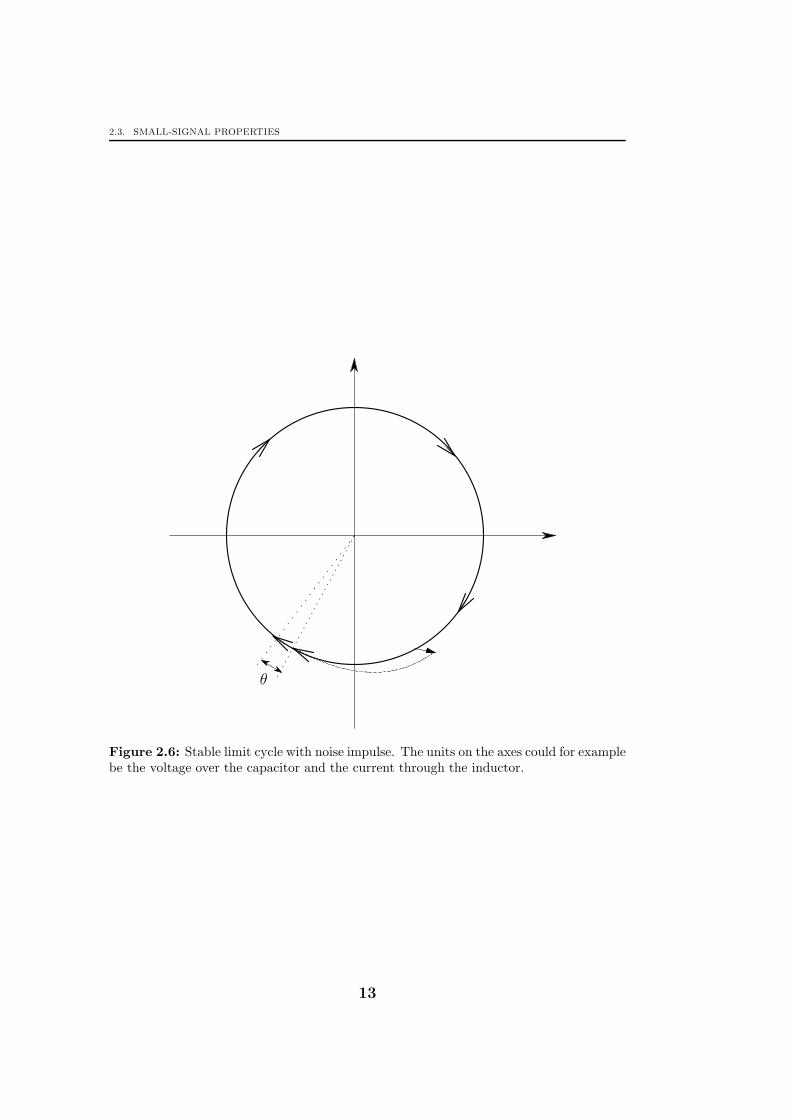
An oscillator has a stable limit cycle as shown in Figure 2.6. A noiseimpulse will move the trajectory from the limit cycle. Due to the amplitude-controlling function of the oscillator, the trajectory will approach the stablelimit cycle with time. However, once it is back on the limit cycle, it may havemoved to a different point compared to if no noise impulse would have beeninjected, with a difference in phase θ. Noise can be modeled as a series ofimpulses with different levels. Consequently, the phase error θ is a functionof time.
12
2.3. SMALL-SIGNAL PROPERTIES
θ
Figure 2.6: Stable limit cycle with noise impulse. The units on the axes could for examplebe the voltage over the capacitor and the current through the inductor.
13
CHAPTER 2. OSCILLATOR BASICS
2.3.1 Amplitude Noise
When a noise impulse causes the amplitude to change, the amplitude-controllingmechanism of the oscillator will correct for this error with time as explainedabove.
The amplitude noise is often less important than phase noise becausemany circuits, such as switching mixers, are less susceptible to amplitudenoise than phase noise. However, in some cases we may have requirementson the amplitude noise as well.
2.3.2 Phase Noise
Oscillators are autonomous systems, i.e. self-timed systems, and cannotcorrect a timing error within the oscillator once it has occurred since thereis no possibility to compare to a true timing value. Hence, any timing orphase errors will accumulate with time and since oscillators are nonlinearand time-variant systems, these timing errors are not easy to calculate.
The phase noise L is defined as follows: the phase perturbation powerin 1 Hz bandwidth at offset ωm from center frequency ω0, normalized to thepower of the fundamental component.
A typical phase-noise spectrum of a free-running oscillator is shown inFigure 2.7. Beginning to the right we have a phase-noise floor. To the leftof this region, we have phase noise which is inversely proportional to thesquare of the offset frequency ωm. The cause of this noise is the white noisein the oscillator components. Further to the left, phase noise is inverselyproportional to the cube of the offset frequency. The cause of this noiseis the 1/f noise in the components that is upconverted to the oscillationfrequency. The corner frequency between the 1/ω2
m region and the 1/ω3m
region is termed ωm,1/f . At low offset frequencies the phase-noise spectrumlevels out.
The phase noise affects Radio Frequency (RF) circuits in several ways; itaffects the transmitted spectrum, the signal constellation, and the Signal-to-Noise Ratio (SNR) after downconversion [Mehrotra and Sangiovanni-Vincentelli,1999]. The timing jitter affects sampling circuits since there is now an un-certainty in the sampling instants, see Figure 2.8. If the sampling occursat different time instants than what one expects, there is an error in thesampled value compared to the true value at the wanted sampling instant ifthe sampled signal has changed between the wanted and the actual samplinginstants.
14

2.3. SMALL-SIGNAL PROPERTIES
ωm,1/f
ωm (log)
L[ωm]
∼ 1/ω3m (-30 dB/dec)
∼ 1/ω2m (-20 dB/dec)
Figure 2.7: Phase noise of sinusoidal oscillator as a function of offset frequency.
Reference
Figure 2.8: Timing jitter in oscillator with squarewave output.
15

CHAPTER 2. OSCILLATOR BASICS
AM-to-PM Conversion
Even if the amplitude noise per se is unimportant in many applications,it may be converted into phase noise through a process called AM-to-PMconversion. This conversion occurs, for example, when a nonlinear capacitoris used for frequency tuning. When the voltage amplitude increases, thecapacitance is affected and the frequency changes. Frequency error and phaseerror are coupled since the instantaneous frequency is the time-derivative ofthe phase.
2.3.3 Injection Locking
Injection locking may occur in oscillators when an input signal of sufficientmagnitude is injected and the oscillation frequency changes from the free-running frequency to that of the injected signal [Adler, 1946, Kurokawa,1973]. The injected signal must be close enough to one of the multiples ofthe fundamental free-running frequency for an injection lock to occur.
In some cases the injection locking is desired, as in some radio receivers,but in other cases it might be a problem, as when the oscillator locks to adisturbance from nearby circuitry.
2.4 Specifying an Oscillator
Before an oscillator can be designed, we must know what the requirements onthis particular oscillator are. Foremost, we have the functional specification:the oscillator should produce a certain waveform at a given frequency. Inaddition there are requirements on design properties which specifies howmuch the function may deviate from the desired one, for example expressedas phase noise spectrum. There are usually additional design constraints dueto the application in which the oscillator is to be used. One typical suchconstraint is the supply voltage. Finally, we usually have a cost function, forexample minimization of power consumption.
A list of requirements could be as follows:
• Center frequency and frequency stability
• Frequency tuning range
• Phase noise / Timing jitter
• Immunity to disturbances (supply, load variations, substrate)
16

2.5. DESIGNING AN OSCILLATOR
• Power consumption
• Supply voltage
• Output waveform
• Start-up time
• Cost (price/size/design time)
• . . .
All these requirements should generally be fulfilled over fabrication vari-ations, component aging and temperature variations.
2.5 Designing an Oscillator
So: how do we now design an oscillator to the given requirements, or formu-lated differently: how do we implement the oscillator in electronic buildingblocks such as transistors, resistors, capacitors and inductors? We must fromthe specification determine
• Circuit topology
• Method for amplitude control
• Frequency tuning implementation
• Component values
• . . .
Not only do we want to create an oscillator that fulfills the specification,we also want to do it in as short design time as possible while still guaran-teeing proper function. This task is far from easy, but it is not unique forthe design of oscillators; the same question arises in all electronic design. Ifwe manage to achieve orthogonality between the design properties, we candesign for each of these properties individually and hence simplify the designprocess considerably since we only have to look at one property at a time.In addition, we should do this in a systematic way not to forget any require-ments. If complete orthogonalization is achieved we may design the oscillatorin a top-down fashion without any iterations, guaranteeing very short designtime indeed.
17

CHAPTER 2. OSCILLATOR BASICS
18

Chapter 3Oscillator Design Methodology
T he proposed oscillator design methodology is described in this chapter.Together with Chapter 4, which contains the derivations, it providesall the information necessary to design an oscillator in a systematic
way.
Following the description of the design methodology, three design exam-ples with different specifications are presented. Using the proposed designmethodology, I design each oscillator according to specification in great de-tail to show how each step in the design methodology is carried out. Finally,I discuss whether it is possible to show if the design methodology will workin all cases or not.
3.1 Introduction
An oscillator design methodology should facilitate the design of a function-ing oscillator which fulfills the specification over manufacturing variations,temperature variations and aging of components; and it should preferablyminimize the design time and effort. It should also indicate, as early as pos-sible in the design process, whether a design specification is attainable ornot. Finally, it should preferably be based on analytical expressions simpleenough to be understood and hand calculated in order to give the designerthe insights needed.
The design methodology described in this chapter fulfills these require-ments for many types of oscillators encountered today. It is useful both forthe design of LC oscillators, with or without frequency tuning, and for thedesign of crystal oscillators. The design methodology also provides a macromodel for the phase noise as a function of the power consumption and im-
19

CHAPTER 3. OSCILLATOR DESIGN METHODOLOGY
plementation process to be used during the overall system design.When developing a design methodology, one usually strives to attain or-
thogonality between the different requirements. If orthogonality is achieved,each of the requirements can be designed for separately and one can con-centrate on one goal at the time, according to the principle of divide andconquer. This division speeds up the design process considerably.
However, the orthogonality should not come at the expense of too muchperformance. It is often reasonable to lose some performance if we get a de-sign that still fulfills the specification, especially if the design time is short-ened. However, if the design requirements are tough to fulfill, the perfor-mance loss may not be acceptable. The design methodology presented inthis chapter strives to achieve orthogonality whenever the performance isaffected to a lesser extent, but in the cases where substantial performancemust be sacrificed some requirements are considered simultaneously.
The design methodology targets harmonic oscillators where the require-ments on output waveform and absolute frequency accuracy are modest andthe primary cost function is the power consumption. High requirements onoutput waveform and absolute frequency accuracy preclude the use of transis-tors operating in a nonlinear fashion with high voltage amplitudes and highpower efficiency, but most oscillator designs do not have these requirements.
3.2 Methodology
We now introduce the design methodology, which is based on the followingsteps:
1. Specification Attainable?
2. Topology Selection
3. Initial Component Sizing
4. Simulation and Optimization
5. Implementation and Verification
The work in this thesis is aimed at the first three steps, after which wehave attained an oscillator topology with an initial sizing of all components.The last two steps are not part of the work in this thesis and are describedelsewhere in the literature.
In the first step, we choose the implementation process and check if thespecification is possible to fulfill. If the specification appears to be impossible
20

3.2. METHODOLOGY
or close to impossible to achieve, we must reassess the considerations we usedwhen we came up with the specification for the oscillator.
In the second step, we derive which topology to use, that is, which typesof components to use and how to connect them together.
In the third step, we choose values for all the components that make upthe oscillator. In case of a discrete implementation, we choose which resistors,capacitors, inductors, transistors, etc, to use, and in the case of an integratedimplementation, we size all components.
3.2.1 First Step: Specification Attainable?
Before we start our design effort we need to know if the specification ispossible to fulfill using the chosen implementation process, or which im-plementation process to choose if there is a choice among several availableimplementation processes.
The minimum achievable phase noise due to the white noise in the oscil-lator itself, Lmin, is given by
Lmin[ωm] =kBT
2PDCQ2
ω20
ω2m
, (3.1)
where ωm is the frequency offset, ω0 is the oscillation frequency, PDC isthe power consumption, Q is the oscillator Q-value, kB is the Boltzmannconstant, and T is the operating temperature. This expression is furtherdiscussed at the end of this section.
We use the concept of Oscillator Design Efficiency (ODE) [van der Tangand Kasperkovitz, 2000] and define the oscillator design efficiency, Υ, accord-ing to
Υ =Lmin[ωm]
L[ωm], (3.2)
where L is the actual phase noise of the oscillator and where the ODE, Υ,is less than unity (negative when expressed in dB), see discussion at the endof this section. For most good oscillator designs, the ODE ends up in theorder of 1% to 10% (-20 dB to -10 dB). How large the ODE is depends onthe requirements: a small tuning range and low component spread tend toincrease it, but a higher oscillator design efficiency than -10 dB is hard toachieve in all cases. On the other hand, it should be possible to have anoscillator design efficiency of at least -20 dB for most specifications.
Usually in an LC oscillator, the Q-values of the inductors dominate thetotal Q-value of the oscillator and the Q-value of the inductors may be takenas a preliminary value for the Q-value of the oscillator. In a crystal oscillator,
21

CHAPTER 3. OSCILLATOR DESIGN METHODOLOGY
the Q-value should be set by the crystal, and as a preliminary value the Q-value of the crystal operating with the intended capacitive load may be used.
Using the requirements on phase noise, power consumption and the esti-mated Q-value, we can now determine if it is possible to design an oscillatorwith these requirements by calculating the oscillator design efficiency, andwe can also get an estimation of how hard it will be to design. The tough-est requirement for the oscillator phase noise should be used when severalrequirements are given, and since the Q-value of components often changeswith temperature, the minimum Q-value should be used. However, just be-cause the specification passes this test does not necessarily means that itis possible to build the oscillator since there are usually more requirementsinvolved.
If the oscillation frequency should be adjustable during operation, wemust make sure that there are varactors that fulfill the requirements on Q-value and capacitance ratio needed for the tuning range. Sometimes it may bewise to split the tuning range into several smaller tuning ranges as describedlater. When splitting the frequency tuning range, the requirements on thevaractors usually are relaxed.
If the specification seems possible to fulfill, we proceed to the next stepin the design process. First, we discuss a few more matters regarding theOscillator Design Efficiency (ODE), which will come in handy later duringthe design process.
The phase noise due to white noise is calculated in Chapter 5 to be
L[ωm] ≈ kBTF
2P1Q2
ω20
ω2m
, (3.3)
where P1 is the power at the oscillation frequency dissipated in the feedbacknetwork and F is the noise factor. Using (3.3), we see that the oscillatordesign efficiency is given by
Υ =η
F, (3.4)
where F is the noise factor and η is the power efficiency defined as
η =P1
PDC. (3.5)
Optimizing an oscillator from the white noise point of view is seen to be theprocess of maximizing the fraction η/F , which is always less than unity (0dB) because F ≥ 1 and η ≤ 1. Hence, Lmin gives a lower bound for thephase noise.
22

3.2. METHODOLOGY
3.2.2 Second Step: Topology Selection
We shall now select a topology that fulfills our requirements on the oscillatorusing the chosen technology/components. The choice of a differential or asingle-ended topology is made based on information on surrounding circuitsand supply/ground/substrate disturbances. In general, integrated oscillatorsare implemented as differential circuits since the environment is noisy and theoscillator shares the substrate with other circuitry. Discrete oscillators areusually implemented as single-ended circuitry to keep the component countlow and hence the price and size down.
Once we have chosen the type of transistors to use and whether we are go-ing for a single-ended or differential topology, it is time to design the feedbacknetwork and bias the active part. These two tasks are done simultaneouslysince the feedback network is an integral part of the biasing network; theinductors and capacitors of the feedback network may act as coupling anddecoupling components in the biasing arrangement. The feedback networkis usually chosen as simple as possible since more complicated networks addpoles and zeros to the loop transfer function and make the amplitude stabilityof the oscillator harder to guarantee.
The ground datum is chosen based on information about parasitic ele-ments, such as stray capacitances and inductances, and the tuning circuitry.For example, in an integrated oscillator many components share the samesubstrate which is usually connected to the supply ground. We must alsotake into consideration whether the voltages are allowed to swing above thesupply voltage or not. External noise sources, such as supply noise, alsoaffect the choice of grounding strategy. The inherent minimum phase noiseof the oscillator is also affected by this choice, as seen in Section 4.4, but inmany cases the other aspects mentioned above are more important.
We next focus on the frequency tuning. As mentioned above, the com-ponents used to perform the frequency tuning, usually voltage-dependentcapacitors such as MOS structures or reverse-biased diodes, play a part indetermining the feedback network to use and the grounding strategy. Thereason for this restriction is that the varactors often need to have one ter-minal signal-grounded and that the varactors are sensitive to any voltagechanges over them, including those of unwanted disturbances on for examplesupply lines transferred to the varactor.
We also need to calculate the tuning range needed to cover the frequencyband of interest, taking into account aging, temperature variations and pro-cess variations. If the frequency tuning range turns out to be wide comparedto the center frequency, it may be wise to split the tuning range into sev-eral smaller tuning ranges by implementing part of the tuning capacitance as
23

CHAPTER 3. OSCILLATOR DESIGN METHODOLOGY
fixed capacitors in series with transistors operating as switches. The choiceof splitting may also make the tuning characteristic more linear, which isoften an advantage when using a Voltage Controlled Oscillator (VCO) in aPhase-Locked Loop (PLL). A final advantage of splitting the tuning rangeinto several smaller tuning ranges is that the phase noise decreases since partof the phase noise is an increasing function with ftune
f0Q, where ftune is the
tuning range and f0 is the center frequency. This matter is further discussedin Chapter 6.
The last step in the topology selection is to design an amplitude-determiningnetwork to make the oscillation amplitude independent of component varia-tions during manufacturing. This network may also help to reduce the phasenoise, especially the phase noise due to 1/f noise. The simplest amplitudecontrols use nonlinearities in the transistors or explicit diodes as voltage lim-iters. These types of amplitude controls make the Q-value of the oscillatorindependent of temperature, aging and process variations, unless the biascurrent of the oscillator is changed with for example temperature. When theQ-value is made constant using this type of amplitude limiting, it is reducedto its lowest possible value. Using this type of amplitude control increasesthe phase noise due to the reduction in Q-value, but the design effort is quitelow.
An Automatic Amplitude Control (AAC) does not lower the Q-value ofthe oscillator considerably, but requires much more design effort. Circuitrythat measures the oscillation amplitude as well as circuitry that controls thebias voltages or currents of the oscillator must be designed, and the con-trol loop must be stable and have enough bandwidth while not contributingtoo much noise or consuming too much power. Consequently, this type ofamplitude control is usually used only when simpler methods do not fulfillthe requirements such as for a crystal oscillator with requirement on shortstart-up time.
3.2.3 Third Step: Initial Component Sizing
Once we have designed the topology, it is time to size all the componentsof the oscillator. This task is carried out in several smaller steps. First wedetermine the voltage gain of the feedback network, Z21/Z11, by maximizingthe Oscillator Design Efficiency (ODE), Υ, which is the task as maximizingthe fraction η/F , where η is the power efficiency and F is the noise factor. Inaddition to the voltage gain, we also determine all bias voltages and currentsand the oscillation amplitudes at the input and output of the active network.Some useful expressions for different topologies are available in Section 4.4.
One important source of noise not covered above is the noise of series base
24
3.2. METHODOLOGY
and gate resistances. As shown in Section 7.2.3, the phase noise due to theseries base and gate resistances depends on the levels of harmonics generatedin the active device. Since the FET has significantly weaker nonlinearitythan the BJT, this source of noise is mostly a problem of oscillators basedon BJTs. From (7.23) we have that
RI
ℜ[Z11]
ℜ[Z11]2
Z221
∞∑
n=1
n2|Fn|2
|F1|2≪ 1 (3.6)
in order for this additional phase noise to be negligible, where RI is the seriesbase or gate resistance and Fn is the describing function for the active part.
For an oscillator based on a single BJT stage, we use (C.24) to get
RI
ℜ[Z11]
ℜ[Z11]2
Z221
4
9
(Vin,1VT
) 32
≪ 1 (3.7)
and for a BJT differential stage, we use (C.46) to get
RI
ℜ[Z11]
ℜ[Z11]2
Z221
1
4
Vin,1VT
≪ 1, (3.8)
where in both expressions Vin,1 is the input-voltage amplitude to the activenetwork. If these inequalities are not fulfilled, the choice of the voltage gainZ21
Z11must be reassessed, this time taking also the series base resistance into
account.
Once the phase noise due to white noise sources has been designed for,we focus on the phase noise due to 1/f noise. The noise corner between phasenoise due to white noise and phase noise due to 1/f noise is given by (7.96)as
ωm,1/f =2π(K1/f,f +K1/f,b)IDCP1
4kBTF
(KAM−PM
1
B
∂B
∂IDC+
∂ζ
∂IDC
)2
, (3.9)
where K1/f,f is the 1/f noise constant of the active network, K1/f,b is the1/f noise constant of the bias network, IDC is the bias current, P1 is thefundamental power delivered to the feedback network, KAM−PM is the AM-to-PM conversion, B is the amplitude gain of the active network and ζ is thephase shift of the active network.
We choose to size the transistors to maximize their transit frequency, fT ,and in the cases where there is a current density that gives a peak fT , sizethe transistors to get that current density. This choice makes ∂ζ
∂IDCsmall
25
CHAPTER 3. OSCILLATOR DESIGN METHODOLOGY
and minimizes the phase noise contribution from induced gate noise. Alsoassuming that ∂B
∂IDC≈ B
IDC, we get the noise corner as
ωm,1/f ≈ 2π(K1/f,f +K1/f,b)P1
4kBTFIDCK2AM−PM , (3.10)
which can be rewritten as
ωm,1/f ≈2π(K1/f,f +K1/f,b)ΥVDC
4kBTK2AM−PM , (3.11)
where Υ is the Oscillation Design Efficiency (ODE) and VDC is the supplyvoltage. We see that there is two principal methods to reduce the phasenoise due to 1/f noise: choose components with low inherent 1/f noise toget low K1/f , and reduce the AM-to-PM conversion, |KAM−PM |. We assumethat Υ is set by requirements on phase noise due to white noise. Since wealready have requirements on the speed of the transistor, we cannot makethem larger to reduce the inherent 1/f noise, but we could for example choosePMOS transistors if they have much lower 1/f noise than NMOS transistors.What remains is the AM-to-PM conversion coefficient which is minimized bythe use of a strong amplitude control as explained in Chapter 5.
3.2.4 Fourth Step: Simulation and Optimization
Once we have an initial sizing of all components, we may commence simu-lation of the oscillator to determine if it is working as intended. We maynow also tweak the component values to optimize the performance. Sincethe simulator usually includes more details in its component models, the re-sults will probably differ somewhat from the hand-calculated ones, but theerror should not be large since most essential component characteristics areincluded in the design methodology. The hand calculations used during thedesign process are never better than the models used during these calcula-tions. The same conclusion is also true for simulators; the simulation resultsare never better than the accuracy of the component models.
3.2.5 Fifth Step: Implementation and Verification
The last step in the design process is to actually build the circuit and measureit to verify the actual performance. This verification phase can be quite timeconsuming, especially if a high confidence that the design meets the specifi-cation over temperature and process spread in mass production is needed.
26

3.3. DESIGN EXAMPLES
3.3 Design Examples
The design methodology outlined above is applied to three design examples inthis section. Design examples with different specifications are carried out tohighlight different aspects of the design methodology. Before studying thesedesign examples in detail, it is recommended to read through Chapter 4.
3.3.1 Crystal Oscillator
The first design example is a crystal oscillator. The oscillator may be usedas a stable frequency reference with low phase noise.
Specification
Design a crystal oscillator using the crystal with specifications given below.The phase noise and power consumption should be minimized. The supplyvoltage is 5.0 V and the temperature operating range is −25C to 80C.
The crystal has the following specifications: f0 = 6.144 MHz, CL = 16 pF,R1 = 30 ∼ 50 Ω, C0 ≈ 4 pF, C1 ≈ 14 fF, Pmax = 100 µW.
First Step: Specification Attainable?
As the first step in the design process, we calculate what performance weexpect to verify that the design specification makes sense.
The maximum drive level for the crystal was given as Pmax = 100 µW.Since we will minimize power consumption and we have an ideal power sup-ply, we will probably end up with a power efficiency, η, in excess of 10%.Hence, the power consumption, PDC, will probably not exceed 1 mW. Con-sequently, the currents will be low and impedances high, which might posea problem later on in the design process.
We conclude that the specification seems attainable and proceed withthe topology selection. Before proceeding with the design, we estimate theresulting phase-noise performance, which is limited by the crystal.
To calculate what phase-noise performance we might expect to get, weneed to estimate the Q-value. From (4.7) we get the minimum series Q-value,QS, as 37000 when R1 is 50 Ω. From (4.47) we get the minimum Q-value forthe oscillator as 23700. In reality, we may have an even lower Q-value due toadditional losses and parasitic capacitances parallel to C0. However, we usethe calculated value for now to estimate the phase noise of the oscillator.
Using (3.3) we get the minimum achievable phase noise at room tem-perature (25C) as −138.6 dBc at 10 Hz offset by assuming that the noise
27

CHAPTER 3. OSCILLATOR DESIGN METHODOLOGY
CC CA
XB
(a) AC schematic.
RC
RERB1
RB2
(b) DC schematic.
Figure 3.1: AC and DC schematics for crystal oscillator.
factor, F , is unity, the Q-value, Q, is that given above and that P1 is Pmaxequal to 100 µW. Due to the reduction in Q-value mentioned in the previousparagraph and the noise factor, F , we expect the phase-noise performanceto be worse by approximately 3 dB to 10 dB, depending on the quality ofthe other components.
Second Step: Topology Selection
Since we are building a discrete circuit, we go with a single-ended solutionbased on a BJT. As described in Section 4.1.7, a crystal network can bedesigned by replacing one of the inductors in an LC network by a crystal.From Section 4.1.6 we have that LCL and CLC networks are the only twonetworks with the right sign for the transfer impedance when we go for asingle-ended circuit. We prefer the CLC network over the LCL networksince it is easier to bias and has fewer inductors. The chosen AC topology isshown in Figure 3.1(a).
The next step is to bias the bipolar transistor. A general biasing schemefor a one-transistor topology using resistors is shown in Figure 3.1(b). Theemitter current is determined by the emitter resistor, RE , and the voltagepotential at the base, which in turn is set by the two resistors RB1 and RB2.The collector voltage potential is set by the emitter current and the collectorresistor, RC .
We now need to determine which node should be the ground datum. Thecrystal does not need to have any lead grounded and we may hence choseto signal-ground the emitter node. This choice gives a higher Q-value sincethe parasitic capacitances CP1 and CP2 in the crystal, see Section 4.1.4, donot end up parallel with C0. By signal-grounding the emitter, we place these
28

3.3. DESIGN EXAMPLES
parasitic capacitances in parallel with to CA and CC . The full schematic isshown in Figure 3.2 where we have added the capacitor CE to signal-groundthe emitter.
RC
RE
RB2 XB
RB1 CC CACE
Figure 3.2: Complete schematic for crystal oscillator.
We might want to replace the resistor RC with an inductor or add aninductor in the base biasing network to provide a higher AC impedance. Itis also possible that we need to add a capacitor in series with the crystalif the series capacitance of CA and CC is higher than the prescribed loadcapacitance CL. We will know if these modifications are needed once we havecalculated the component values in the next step of the design methodology.
The remaining topology decision is the means for amplitude control. Sincethe power consumption is very low and we do not have any requirementon the start-up time, we do not gain much by using an explicit amplitudecontrol. Consequently, we choose diode limiting amplitude control using thebase–collector diode, because this way we avoid adding another component.
Third Step: Initial Component Sizing
We first need to decide which transistor to use. We want a transistor with lowseries base resistance and low parasitic capacitances. A transistor fulfillingthese requirements is the NPN transistor 2N2369 with the following data:CBE ≈ 3 pF, CBC ≈ 3 pF, rbb ≈ 10 Ω and β ≈ 40.
The capacitance CBC is parallel to C0 of the crystal and needs to besubtracted from CL. Introducing C ′
L as the remaining capacitance, we have
CL = CBC + C ′L (3.12)
with C ′L = 13 pF in our case. From (4.47), we get the Q-value of the oscillator
as
Q ≈ QS
(C ′L
C0 + CBC + C ′L
)2
≈ 15600. (3.13)
29

CHAPTER 3. OSCILLATOR DESIGN METHODOLOGY
From (4.49) and (4.45), we have that the Q-value of the capacitors mustfulfill
QC ≫ C1
2(C0 + CL)Q ≈ 5.5 (3.14)
in order not to degrade the Q-value, which should not pose any difficulties.We will for now assume that this inequality is fulfilled and check it later.
The next step in the choice of components is to calculate the Z-parametersof the feedback network in order to calculate the capacitances. The funda-mental power delivered to the feedback network is given by
P1 =V 2out,1
2Z11
. (3.15)
The fundamental power, P1, was given to be less than 100 µW in the specifi-cation so we need to choose Vout,1 to get a value for Z11. We can already nowsee that it is not practical to replace RC with an inductor. The impedance ofthis inductor would need to be very high since the impedance levels are veryhigh due to the low power consumption. Consequently the output voltagecannot swing above the supply voltage. From (4.56) we have
|Vout,1| ≈ Vc,0 − Ve,0 − VCE,min, (3.16)
where VCE,min is approximately 0.2 V. We choose Ve,0 = 1.8 V for good biasstability and small shift in bias current during start-up. A higher value wouldgive better stability but lower power efficiency and higher power consump-tion. We also choose
Vc,0 = VDC − |Vout,1| (3.17)
to maximize the output amplitude and thereby the efficiency. Combiningthese two last equations we get
|Vout,1| =VDC − Ve,0 − VCE,min
2= 1.5 V. (3.18)
We can now calculate Z11 as
Z11 =V 2out,1
2P1
≈ 11.3 kΩ. (3.19)
From (4.19) we have
Z11 ≈X2A
RS, (3.20)
where
RS ≈ R1
(C0 + CBC + C ′
L
C ′L
)2
≤ 118 Ω (3.21)
30

3.3. DESIGN EXAMPLES
from (4.48). Hence, we get XA = −1.15 kΩ and
CA = − 1
ω0XA≈ 22 pF. (3.22)
We now need to determine the fraction Z11
|Z21| in order to calculate CC . Ahigh fraction gives us higher QC and lower bias variations during start-up buthigher phase noise, see Figure 4.19(c). As a compromise, we choose a valueof 3 which gives only a slight degradation of the phase-noise performance.From (4.23) we have
Z21
Z11
≈ −XC
XA
= −CACC
, (3.23)
giving us XC ≈ −384 Ω and CC ≈ 67 pF.Calculating the series connection of CA and CC , we get a load capacitance
for the crystal of 17 pF which is higher than the wanted value C ′L=13 pF.
Since the value is only slightly higher than the wanted, we choose to modifyCA and CC instead of adding a capacitor in series with the crystal. Thischoice gives us slightly lower power P1, but one component less. The newvalues are CA = 18 pF and CC = CBE + 47 pF, where we have chosencapacitors from the E12 series. The new reactances are XA = −1.44 kΩand XC = −520 Ω and the new input impedance to the feedback network isZ11 = 17.5 kΩ.
Assuming that |Vout,1| ≈ 1.5 V, we get |Iout,1| = 86 µA and from (4.147)we have Ic,0 = 43 µA. We also have
RC =VDC − Vc,0
Ic,0=
|Vout,1|Ic,0
≈ 35 kΩ (3.24)
and choose RC = 36 kΩ from the E24 series. The Q-value for ZA thenbecomes 25, which fulfills the requirement on QC . We also have
RE =Ve,0Ie,0
≈ Ve,0Ic,0
≈ 41.9 kΩ (3.25)
and choose RE = 39 kΩ from the E24 series.We proceed with the bias resistors RB1 and RB2. The DC voltage at the
base terminal is given by (4.55) as
Vb,0 = Ve,0 − |Vin,1| + VBE,max ≈ 1.9 V, (3.26)
where we have assumed that VBE,max = 0.6 V. During start-up we will have|Vin,1| = 0 which gives Ve,0 ≈ 1.3 V and Ie,0 ≈ 33 µA. This start currentcorresponds to a small-signal loop gain of 7.5 at room temperature. The
31

CHAPTER 3. OSCILLATOR DESIGN METHODOLOGY
current through RB1 should be at least ten times higher than the base currentfor good bias stability, which corresponds to a current of at least 11 µA.Higher current gives lower resistances, which in turn gives a lower Q-valuefor CC . We choose RB1 = 160 kΩ and RB2 = 240 kΩ. The parallel connectionof RB1 and RB2 is 96 kΩ which gives a Q-value of 185 for CC – well abovethe required minimum Q-value.
The last component to size is the capacitor CE. The reactance from thiscomponent must be much less than XA and XC at the oscillation frequency.A capacitance of 10 nF gives a reactance of −2.6 Ω.
The current consumption may be found by adding the emitter DC currentand the current flowing through RB1, 46 µA and 12 µA, giving a total currentconsumption IDC = 58 µA. The power efficiency is given by
η =Ie,0IDC
Vout,1VDC
≈ 24%. (3.27)
The total power consumption is 290 µW and the power delivered to thecrystal is 67 µW. We also calculate the peak current from (C.23) to beapproximately 500 µA which should not cause any problems.
We check if the base resistance is low enough to give negligible contribu-tion to the phase noise. Using (3.7), we have
rbbZ11
Z211
Z221
4
9
(Vin,1VT
) 32
≈ 0.2, (3.28)
which gives negligible contribution to the phase noise. The noise factor forthe oscillator is given by (4.173) as
F ≈ 1 +1
2
Z11
|Z21|≈ 2.5, (3.29)
and if we add the contribution from the base series resistance, we get a noisefactor of 2.7. The Oscillator Design Efficiency (ODE) can now be calculatedfrom (3.4) to be −10.7 dB, which is very good considering that the design isdone without inductors. We calculate the minimum achievable phase noise,Lmin, from (3.1) to be −139.6 dBc/Hz at 10 Hz offset for the calculatedpower consumption. The phase noise can now be calculated using (3.2) tobe −128.9 dBc/Hz at 10 Hz offset.
If we had the requirement that the oscillation amplitude must be verystable, we could increase the current consumption to make the amplitudelimiting stronger at the expense of higher power consumption.
32

3.3. DESIGN EXAMPLES
Fourth Step: Simulation and Optimization
We simulate the oscillator, including measurement buffers, to verify the func-tionality. We get an output-voltage amplitude, Vout,1, of 1.102 V and aninput-voltage amplitude, Vin,1, of 0.402 V. The simulated current consump-tion is 56.5 µA and the simulated phase noise is −132.1 dBc at 10 Hz offset.
We deem the simulated performance to be satisfactory and proceed withthe implementation of the oscillator.
Fifth Step: Implementation and Verification
The oscillator was built and measured. The measured current consumptionwas 54 µA at 5.0 V supply and the oscillation frequency was 6.146 MHz.The phase noise could not be measured due to lack of instruments capableof measuring such low phase noise.
Summary
The performance of the crystal oscillator in room temperature is summarizedin Table 3.1. The calculated, simulated and measured values agree quitewell. It was, unfortunately, not possible to measure the phase noise of theimplemented oscillator.
Table 3.1: Performance of crystal oscillator.
spec. calc. sim. meas. unit
IDC min.a 58 57 54 µAL @ 10 Hz min.b −128.9 −132.1 ?c dBc/Hz
aThe current consumption should be minimized once the phase noise has been mini-mized.
bThe phase noise should be minimized subject to constraint on maximum power dissi-pated in the crystal.
cCould not be measured with the measurement equipment available.
3.3.2 VCO using JFET
The next design example is a Voltage-Controlled Oscillator (VCO) to be usedin an FM system. The primary function of the VCO is to frequency-modulatethe signal.
33

CHAPTER 3. OSCILLATOR DESIGN METHODOLOGY
Specification
The VCO is part of a loop controlling the average output frequency to100 MHz. The function of the loop is to relate the output carrier frequency tothat of a stable frequency reference, for example a crystal oscillator. The loopbandwidth is much lower than the lowest frequency component of the inputinformation signal and does not interfere with the frequency modulation.
The requirements on the modulation is as follows: full modulation of75 kHz, input modulation bandwidth from 30 Hz to 15 kHz, and incidentalfrequency modulation of at least 100 dB below full modulation. We alsowant to minimize the power consumed by the VCO, which is supplied froma voltage source of 6.0 V.
We first calculate the requirement on phase noise from the requirementon incidental frequency modulation, βf . From this requirement we haveβf ≤ 0.75 Hz. The maximum allowed phase noise can be calculated from
βf =
√2
∫ fh
fl
f 2mL[fm]dfm (3.30)
to be −127.26 dBc at 10 kHz offset, where we have used fl = 30 Hz andfh = 15 kHz from the specification and assumed that the phase noise originsfrom white noise alone.
First Step: Specification Attainable?
Since the phase-noise performance is specified, we can calculate what powerconsumption will be necessary to fulfill this requirement to see if the specifi-cation makes sense. From (3.1) we have
PDC,min =kBT
2L[ωm]Q2
ω20
ω2m
, (3.31)
which gives us a lower limit of 0.44 mW, assuming that the Q-value of adiscrete inductor is at least 50. Since the ODE probably will be worse than−10 dB, we expect the power consumption, PDC , to be somewhat above5 mW. This power consumption should not pose any problems and we mayproceed to the next step in the design methodology.
Second Step: Topology Selection
We choose to base our design on a JFET, since JFETs are known to havelow 1/f noise and designs based on FETs are less sensitive to series base/gate
34
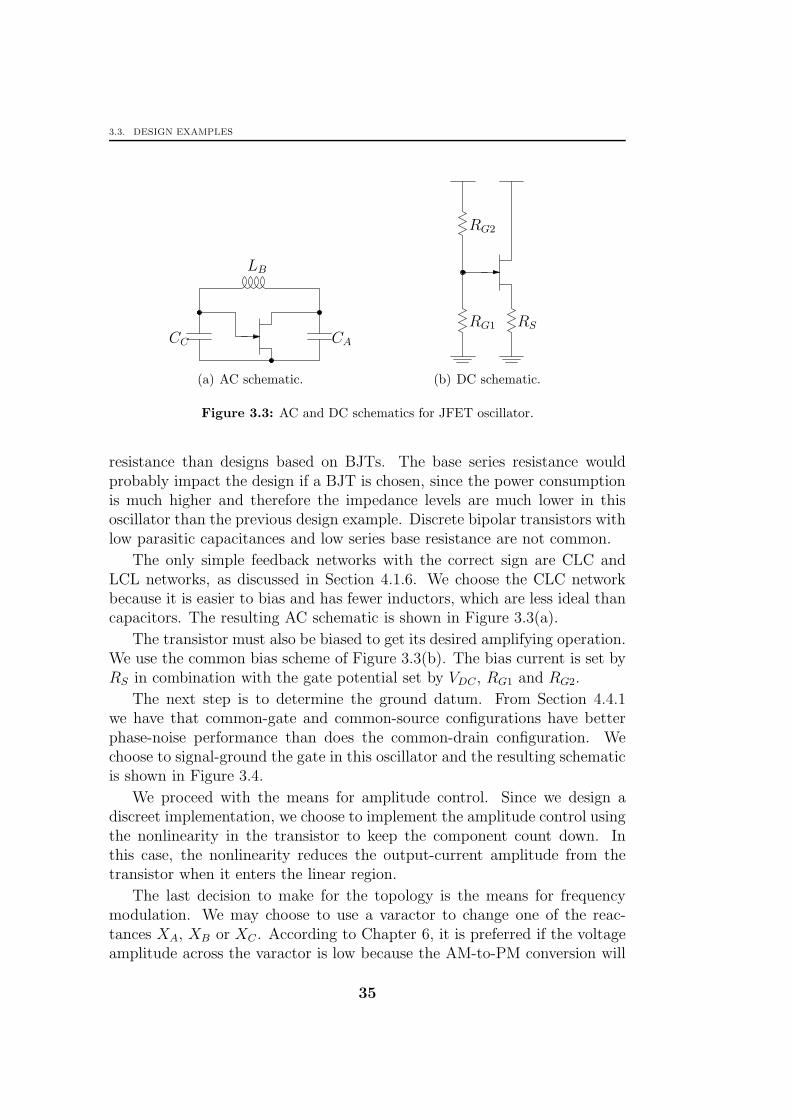
3.3. DESIGN EXAMPLES
CC CA
LB
(a) AC schematic.
RG2
RG1 RS
(b) DC schematic.
Figure 3.3: AC and DC schematics for JFET oscillator.
resistance than designs based on BJTs. The base series resistance wouldprobably impact the design if a BJT is chosen, since the power consumptionis much higher and therefore the impedance levels are much lower in thisoscillator than the previous design example. Discrete bipolar transistors withlow parasitic capacitances and low series base resistance are not common.
The only simple feedback networks with the correct sign are CLC andLCL networks, as discussed in Section 4.1.6. We choose the CLC networkbecause it is easier to bias and has fewer inductors, which are less ideal thancapacitors. The resulting AC schematic is shown in Figure 3.3(a).
The transistor must also be biased to get its desired amplifying operation.We use the common bias scheme of Figure 3.3(b). The bias current is set byRS in combination with the gate potential set by VDC , RG1 and RG2.
The next step is to determine the ground datum. From Section 4.4.1we have that common-gate and common-source configurations have betterphase-noise performance than does the common-drain configuration. Wechoose to signal-ground the gate in this oscillator and the resulting schematicis shown in Figure 3.4.
We proceed with the means for amplitude control. Since we design adiscreet implementation, we choose to implement the amplitude control usingthe nonlinearity in the transistor to keep the component count down. Inthis case, the nonlinearity reduces the output-current amplitude from thetransistor when it enters the linear region.
The last decision to make for the topology is the means for frequencymodulation. We may choose to use a varactor to change one of the reac-tances XA, XB or XC . According to Chapter 6, it is preferred if the voltageamplitude across the varactor is low because the AM-to-PM conversion will
35

CHAPTER 3. OSCILLATOR DESIGN METHODOLOGY
RG2
RG1 CG RS CC
CA
LB
Figure 3.4: Complete schematic for JFET oscillator.
be lower. Since the frequency tuning range is quite moderate, (we only haveto modulate 75 kHz and track slow frequency changes due to temperatureand aging), we choose to control the reactance XC . The new schematic isshown in Figure 3.5, where the capacitance CC now is replaced with a fixedcapacitor C ′
C in parallel with a reverse-biased diode acting as a varactor. Thecapacitance CD provides a low impedance at the fundamental frequency andRD is inserted to filter out noise on the control voltage VC .
RG2
RG1 CG RS
CA
LB
C ′C CD
RDVC
Figure 3.5: Complete schematic for JFET VCO.
Third Step: Initial Component Sizing
Our first choice regards the transistor. Since the operation frequency is quitehigh, we need a transistor with low parasitic capacitances. We also want thetransistor to have small gate–source voltage compared to the supply voltageat the operation current, which we expect to be in the vicinity of 1 mA fromthe first design step. We choose the BF245A n-channel JFET. It has the
36

3.3. DESIGN EXAMPLES
following typical parameters: K = 1 mA/V2, VT = −2 V, CGS = 2.2 pF andCGD = 2.2 pF.
The spread in threshold voltage, VT , for this transistor type is estimatedto be about ±0.5 V from the data sheet. Hence, we choose the source termi-nal DC voltage, Vs,0, to be 2 V to give a stable bias current over componentvariations. From the first step, we estimated the DC current to be about1 mA which gives an overdrive voltage of about 1 V, and consequently theminimum drain–source voltage will be approximately 1 V. We can now cal-culate the output amplitude from (4.56) to be
|Vout,1| ≈ Vd,0 − Vs,0 − VDS,min ≈ 3.0 V. (3.32)
We proceed with the determination of the fraction Z11
|Z21| . We want theinput amplitude to be at least 1 V to guarantee start-up, which requires thatVin,1 > KFETVGT0, see Section 4.2.3. At the same time, we do not want theinput amplitude to be large enough to forward-bias the gate–source diode.Since the input-voltage amplitude is across the diode we get better tuningrange when the fraction is low, but we also get higher AM-to-PM conversion.We choose Z11
|Z21| = 3 to get |Vin,1| = 1.0 V.To calculate the noise factor below, we need to derive the following frac-
tion:
Z11
RS
= Z11Id,0Vs,0
= Z11|Id,1|
2KFETVs,0=
|Vout,1|2KFETVs,0
≈ 1.25, (3.33)
where we have used that |Iout,1| = 2KFETIDC , Vout,1 = Z11Iout,1 and assumedthat KFET ≈ 0.6.
The noise factor is given in (4.113) as
F ≈ 1 + γZ11
|Z21|+Z2
21
Z211
Z11
RS≈ 3.14, (3.34)
where γ = 2/3. The power efficiency can be calculated from (4.51) as
η ≈ KFET|Vout,1|VDC
≈ 0.30. (3.35)
Inserting the noise factor, F , and the power efficiency, η, in (3.4), we get
Υ =η
F≈ 0.096 (3.36)
or −10.20 dB. The phase noise is calculated from (3.1) and (3.2) to be−128.40 dBc at 10 kHz offset.
37
CHAPTER 3. OSCILLATOR DESIGN METHODOLOGY
We can now calculate the power consumption, using the ODE, to be atleast
PDC =PDC,min
Υ≈ 4.6 mW. (3.37)
We choose PDC equal to 6 mW for some extra margin and get the currentconsumption, IDC , as 1 mA. The output-current amplitude, Iout,1, is equalto KFETIDC and becomes approximately 1.2 mA. The input impedance tothe feedback network is given by
Z11 =Vout,1Iout,1
≈ 2.5 kΩ. (3.38)
We can now determine the component values. From (4.19), we have theinput impedance, assuming that the inductor, LB, dominates the Q-value ofthe oscillator, as
Z11 ≈X2A
RB=X2A
XB
XB
RB≈ −QB
X2A
XA +XC, (3.39)
where we in the last stage used (4.18). Using
Z21
Z11
≈ −XC
XA
(3.40)
from (4.23), we get
XA ≈ −Z11
QB
(1 − Z21
Z11
)≈ −66.7 Ω, (3.41)
corresponding to a capacitance of 23.9 pF; we choose the closest value inthe E12 series, which is 22 pF. We also get the reactance XC as −22.2 Ω,corresponding to a capacitance of 71.6 pF. The reactance XB is 88.9 Ω, corre-sponding to an inductance of 141.5 nH. We choose to use an inductor of value134 nH, which together with the inductance of the wires gives approximatelythe wanted inductance.
We proceed with the calculation of the biasing components. The resis-tance RS is given by the fraction of Vs,0 and IDC , giving a value of 2.0 kΩ.This resistance in parallel with the reactance XC gives a Q-value of approx-imately 90 for this reactance, high enough to have only a small impact onthe total oscillator Q-value.
From the transistor parameters we get an overdrive voltage of approxi-mately 1 V, giving a gate potential, Vg,0, of 1.0 V. This voltage is accom-plished by the voltage division between RG1 and RG2. We choose RG1 to
38

3.3. DESIGN EXAMPLES
be 22 kΩ and RG2 to be 100 kΩ. Finally CG is chosen to have much lowerimpedance then XB at the oscillation frequency, for example 10 nF corre-sponding to a reactance of −0.16 Ω.
The last components to be selected are those related to the frequencytuning. We assume that we design for a nominal tuning voltage, VC , of5.0 V. This gives a nominal reverse-bias voltage, V0, of 3.0 V for the diodebecause the source potential, Vs,0, is 2.0 V. The values for the diode usedare CN = 35 pF and ψ = 0.7 V where CN is the small-signal capacitancewhen no reverse bias voltage is applied and ψ is the built-in potential, seeSection 6.5.
The nominal large-signal capacitance, C, of the diode is approximatelygiven by (6.45) as
C ≈ CN√1 + V0
ψ
≈ 15 pF, (3.42)
which means that C ′C is chosen from the E12 series to be 56 pF to give the
total capacitance, CC . We finally choose the decoupling capacitance CD tobe 1 nF to provide a low-impedance path for the fundamental component,and we choose RD equal to 1 kΩ to suppress high-frequency disturbances onthe control voltage VC .
We now want to know what VCO tuning constant, KV CO, we get with thechosen component values. We first calculate the total frequency-determiningcapacitance, C, from (4.32) to be
C =CA(C ′
C + C)
CA + (C ′C + C)
≈ 16.9 pF (3.43)
and the change in total capacitance with respect to the large-signal capaci-tance of the diode is given by
∂C
∂C=
CCA
(C ′C + C)(CA + (C ′
C + C))≈ 0.0536. (3.44)
From (6.43) we have the capacitance parameter C1 as
C1 ≈ − CN√1 + V0
ψ
1
2
(V1
ψ + V0
)≈ −1
2
(V1
ψ + V0
)C ≈ −2.03 pF. (3.45)
We can now calculate the VCO tuning constant from (6.23) as
KV CO ≈ −f0
V1
C1
2C
∂C
∂C≈ 320 kHz/V. (3.46)
39

CHAPTER 3. OSCILLATOR DESIGN METHODOLOGY
We also want to know how large the AM-to-PM conversion is to see ifit has any impact on the phase noise. We first calculate some intermediateresults from (6.32)
∂α
∂ω0
≈ −2Q
ω0
≈ −1.59 × 10⁻⁷, (3.47)
from (6.44)
C2 ≈CN√1 + V0
ψ
(3
16
(V1
ψ + V0
)2)
≈(
3
16
(V1
ψ + V0
)2)C ≈ 0.205 pF,
(3.48)and from (6.22)
∂ω0
∂C=∂ω0
∂C
∂C
∂C≈ − ω0
2C
∂C
∂C≈ −9.96 × 10¹⁷. (3.49)
We can now calculate the AM-to-PM conversion by inserting (6.29) and(6.33) in (6.28) as
KAM−PM ≈ − ∂α
∂ω0
∂ω0
∂CC2 ≈ −0.033, (3.50)
which is small enough to give negligible contribution to the phase noise.
Fourth Step: Simulation and Optimization
The oscillator is simulated together with the measurement buffers to ver-ify the design before implementation. The current consumption is simu-lated to be 1.03 mA, the input-voltage amplitude, Vin,1, is 0.99 V and theoutput-voltage amplitude, Vout,1, is 3.39 V. The phase noise is simulated tobe −127.1 dBc at 10 kHz offset and the VCO gain is 300 kHz/V.
The oscillator does not fulfill the requirement on phase noise, but is veryclose. If the requirement on phase noise was very important, we shoulddesign the oscillator to have some margin to the specification at the expenseof additional power consumption. However, in this case we decide that theperformance is satisfactory and proceed with the implementation.
Fifth Step: Implementation and Verification
As the last step in the design procedure, the oscillator was built and itsperformance was measured. The measured current consumption was 1.06 mAat 6.0 V supply and the oscillation frequency was 99.0 MHz before trimmingof the inductance. The phase noise could not be measured because it ended
40

3.3. DESIGN EXAMPLES
up in the noise floor for the measurement equipment used, but it could benoted that it was less than −115 dBc at 10 kHz offset. The VCO tuningconstant was measured to be 120 kHz/V at a nominal tuning voltage of5.0 V.
Summary
The performance of the JFET VCO in room temperature is summarized inTable 3.2. The calculated, simulated and measured values agree quite well.The only parameter that does not agree well is the measured tuning constant,probably due to errors in the model of the diode and/or additional parasiticcapacitances, which tend to reduce the tuning constant.
Table 3.2: Performance of JFET VCO.
spec. calc. sim. meas. unit
IDC min 1.00 1.03 1.06 mAL @ 10 kHz −127.3 −128.4 −127.1 < −115a dBc/HzKV CO — 320 300 120 kHz/V
aCould not be measured with the measurement equipment available.
3.3.3 Integrated VCO using MOSFETs
The last design example is an integrated Voltage Controlled Oscillator (VCO).The application may be the carrier generation for a mobile communicationsystem.
Specification
A VCO with minimum power consumption integrated in a 0.35 µm CMOSprocess is to be designed. The supply voltage is within the range 3.0 V to3.7 V with a nominal value of 3.3 V. The center frequency should be 800 MHzand a tuning range of 80 MHz is wanted. The phase noise should not exceed−100 dBc at 100 kHz offset and the area must not exceed 0.1 mm2.
41

CHAPTER 3. OSCILLATOR DESIGN METHODOLOGY
(a) DC schematic.
C L
−1
(b) AC schematic.
Figure 3.6: CMOS oscillator.
First Step: Specification Attainable?
The phase-noise performance is specified, so we can calculate what powerconsumption will be necessary to fulfill this requirement. From (3.1) we have
PDC,min =kBT
2L[ωm]Q2
ω20
ω2m
, (3.51)
which gives us a lower limit of 150 µW for the power consumption, assumingthat the Q-value of the oscillator is approximately 3 (estimated using (F.11)and assuming that the inductor is implemented as two separate spiral induc-tors). Since the ODE probably will be in the order of −10 dB to −20 dB, weexpect the power consumption, PDC, to be in the range 1.5 mW to 15 mW.This power consumption is acceptable from thermal stress point of view andwe may proceed with the design of the oscillator.
Second Step: Topology Selection
Since the oscillator is implemented in an integrated circuit, we choose to usea differential solution to minimize the sensitivity to noise from other circuitryon the same chip. No node voltages are allowed to exceed the supply voltagedue to the rapid aging of components when the electric fields get too high.Consequently, we choose to use a complementary topology for the active partwhich also has the benefit of having higher transconductance per currentconsumption and the resulting bias scheme is shown in Figure 3.6(a).
We proceed with the choice of signal grounding. From Section 4.4.1we have that common-gate and common-source configurations have better
42

3.3. DESIGN EXAMPLES
phase-noise performance than common-drain and differential stage configu-rations. We choose to signal-ground the source in this oscillator. We chooseto implement the biasing current source with a PMOS transistor since theyhave lower 1/f noise than NMOS transistors in this process.
We next determine the feedback network. Having a differential topol-ogy, we may choose any one of the feedback networks mentioned in Sec-tion 4.1.6. From Section 4.4.1 we have that the phase-noise performance isbest when Z11
|Z21| = 1 for the chosen signal grounding. We choose the simplestfeedback networks fulfilling our requirements – the parallel LC circuit, seeFigure 3.6(b). We also choose to implement the inductor as two series con-nected integrated inductors to get lower sensitivity to magnetically coupleddisturbances. This choice has the disadvantage of giving lower Q-value perarea for the inductor. The resulting schematic is shown in Figure 3.7. Thecapacitor CB performs the signal grounding of the source terminals of thePMOS transistors.
C CB
L
VBIAS
Figure 3.7: CMOS oscillator.
Since we are building a differential circuit, we need to check the common-mode stability. Using the method discussed in Section 4.2.3, we see that theequivalent common-mode circuit is simply an inverter and there is no risk ofhaving common-mode oscillations.
Next, we design the amplitude control. To keep the design effort low, wechoose to use the inherent nonlinearity of the transistors, in this case theirlinear regions. Consequently, no additional circuitry needs to be added.
43

CHAPTER 3. OSCILLATOR DESIGN METHODOLOGY
Finally, we must implement the frequency tuning. Since we are designingin a CMOS process, we implement the varactors with MOS structures. It maybe necessary to divide the tuning range into several smaller tuning ranges,depending on the requirements on the oscillator. This choice will be madelater once we have the initial values for the components. The full schematicfor the VCO is shown in Figure 3.8.
C
L
VBIAS
VTUNECB
Figure 3.8: CMOS oscillator.
Third Step: Initial Component Sizing
Since the component spread is higher in integrated circuits than discretecircuits, we design with some margin – in this case for a phase noise of−103 dBc/Hz at 100 kHz offset. The fundamental power dissipated in thefeedback network can be calculated from (3.3) to be
P1 ≈kBTF
2L[ωm]Q2
ω20
ω2m
≈ 584 µW, (3.52)
where the noise factor, F , is given by (4.133) as
F ≈ 1 + γ (3.53)
44
3.3. DESIGN EXAMPLES
and we have assumed that γ = 1.The output-voltage amplitude, Vout,1, is twice the value of (4.58), which in
our case is equal to the threshold voltage, VT , which is approximately 0.6 V.The factor two comes from the differential nature of the circuit. The inputimpedance of the feedback network is given by
Z11 =V 2out,1
2P1≈ 308 Ω. (3.54)
From (4.19) we have
Z11 ≈X2L
RL
= QLXL = QLω0L, (3.55)
where RL is the series resistance of the inductor and QL is the Q-value of theinductor defined in (4.6). Solving for the inductance, L, we get 20.45 nH.
The two series-connected inductors are calculated using the expressionsof Appendix F. The inductors are assumed to have octagonal shape with anouter diameter, dout, of 200 µm, a turn width, w, of 6 µm, a turn spacing, s,of 2 µm, and the number of turns, n, is 10.
After the inductor design, we get an inductance, L, of 20.16 nH and a Q-value of 2.81. Assuming that the output-voltage amplitude, Vout,1, is 0.6 V,we have a fundamental power, P1, of 631 µW. Inserting this power in (3.3),we get the phase noise as −102.78 dBc/Hz at 100 kHz offset, which stillfulfills the requirement. The output-current amplitude is given by
Iout,1 =Vout,1Z11
= 2.105 mA, (3.56)
which gives the current consumption using
Iout,1 = KFETIDC (3.57)
as 3.508 mA assuming that KFET = 0.6, see discussion on KFET in Sec-tion 4.2.1. For a supply voltage, VDC , of 3.0 V, we get a power consumption,PDC , of 10.5 mW, a power efficiency, η, of 6.0%, and an ODE, Υ, of −15.2 dB.For a supply voltage of 3.7 V, we get a power consumption of 13.0 mW, apower efficiency of 4.9%, and an ODE of −16.1 dB.
We proceed with the sizing of the transistors. According to Section 4.2.3,we must have
VGT0 ≤Vin,1KFET
≈ 1.0 V (3.58)
to guarantee start-up. We choose VGT0 = 0.7 V and get NMOS transistors ofsize 20 µm
0.35 µmand PMOS transistors of size 60 µm
0.35 µm. The current-source PMOS
transistor has then approximately 0.4 V over it when the DC supply is 3.0 V.
45

CHAPTER 3. OSCILLATOR DESIGN METHODOLOGY
Next, we need to calculate the additional capacitance needed to achieve acenter frequency, f0, of 800 MHz. The total differential capacitance is foundfrom
C ≈ 1
ω20L
(3.59)
to be 1.96 pF. The parasitic capacitances between each node and ground ismade up of the buffers, Cbuf ≈ 800 fF, the active transistors, Cact ≈ 130 fF,and the inductors, Cind ≈ 210 fF. Subtracting these parasitic capacitancesfrom the total capacitance, C, we see that an additional differential capaci-tance of 1.39 pF is needed.
When using integrated capacitors, we need to take the additional para-sitic capacitance to the substrate, which is grounded, into account. In thistechnology, the parasitic capacitance is approximately 1/7 of the capacitancebetween the two plates. To get a total differential capacitance of 1.39 pF wecan insert four capacitances with capacitance 330 fF, which gives the wantedcapacitance when the additional parasitic capacitance is taken into account.
The capacitor CB provides a low-impedance path for the higher harmon-ics. Choosing a capacitance of 2 pF gives an impedance of 100 Ω at 800 MHz.All bias and supply voltages are also capacitively decoupled.
Finally, we must design the frequency tuning network. We now replacesome of the frequency-determining capacitance with varactors. We choose touse PMOS transistors as inversion-mode varactors since there are no dedi-cated varactors available in the chosen process.
We first need to calculate if we need to split the tuning range into severalsmaller ranges or if we can implement it as only one tuning range. Thelimiting factor is the AM-to-PM conversion which upconverts 1/f noise tophase noise. Assuming that the noise corner fm,1/f is not higher than 100 kHzin order to fulfill the phase noise specification, we can calculate the allowedAM-to-PM conversion from (3.11) as
|KAM−PM | ≈√
4kBTfm,1/f(K1/f,f +K1/f,b)ΥVDC
. (3.60)
In this process the NMOS transistors have much higher noise than the PMOStransistors and we calculate the 1/f noise constant, K1/f , for the NMOS tobe 1.8 × 10⁻¹² A. Inserting this value in (3.60), we get that |KAM−PM | isapproximately 0.10. We can now calculate the allowed tuning range from(6.62) to be
ωtuneω0
≈ π|KAM−PM |2Q
≈ 0.056, (3.61)
46

3.3. DESIGN EXAMPLES
where we have assumed that the feedback network is fairly linear and thatthe amplitude limiting makes the absolute incremental large-signal loop gainmuch smaller than one. We see that the tuning range cannot be largerthan 5.6% and we consequently need to split the tuning range into severalsmaller tuning ranges. The question is: How many of these smaller tuningranges are needed? We note that each step must be smaller than the tuningrange because we need some overlap. We also note that the total tuningrange should be approximately 30% since we want a tuning range of 10%and we add an additional 20% to accomodate process variations and processuncertanties. The additional tuning range may be reduced if a test VCO isdesigned and measured upon to remove the systematic errors. We chooseto make the frequency steps approximately 4% to get some overlap and stillonly a few frequency steps to cover the entire tuning range.
Now we size the varactor. From (6.61) and (6.21) we have
CH − CLC
≈ 2ωtuneω0
, (3.62)
which together with the process parameters indicate that using two PMOSvaractors of size 260 µm
0.5 µmgives the wanted tuning range. The capacitors that
are used to give the frequency steps in tuning range are also implementedas PMOS varactors. Calculating the size to give nine frequency ranges andthe middle range for the wanted frequency, we get varactors of size 190 µm
0.5 µm.
We also calculate the resulting maximum VCO tuning constant, KV CO, from(6.23) and (6.58) to be
max |KV CO| ≈ −ω0
V1
|CH − CL|πC
≈ 54 MHz/V. (3.63)
Fourth Step: Simulation and Optimization
We first simulate the oscillator without frequency tuning, that is, with inte-grated poly–poly capacitors. The simulated phase noise is −108.1 dBc/Hz at100 kHz offset with a supply voltage of 3.7 V and a supply current of 3.5 mA.This simulated phase noise is much better than the specification requires andwe might want to redesign the oscillator to bring the power consumptiondown at the expense of higher phase noise. The simulated single-sided oscil-lation amplitude is 0.639 V, which is close to the calculated value of 0.6 V.We choose to implement the oscillator with the values calculated above.
We proceed with the simulation of the VCO including the varactors. Weincrease the current consumption somewhat to 4.0 mA to compensate for thelosses in the varactors and to guarantee operation over the entire frequency
47
CHAPTER 3. OSCILLATOR DESIGN METHODOLOGY
1 1.5 2 2.5 3 3.5 4740
760
780
800
820
840
860
880
900Frequency
Tuning voltage [V]
Fre
quen
cy [M
Hz]
(a) Simulated oscillation frequency asfunction of tuning voltage.
1 1.5 2 2.5 3 3.5 4−60
−50
−40
−30
−20
−10
0
10
Tuning Constant KVCO
Tuning voltage [V]
Tun
ing
cons
tant
[MH
z/V
]
(b) Simulated tuning constant as functionof tuning voltage.
1 1.5 2 2.5 3 3.5 4−110
−109
−108
−107
−106
−105
−104Phase Noise @ 100 kHz offset
Tuning voltage [V]
Pha
se n
oise
[dB
c/H
z]
(c) Simulated phase noise as function oftuning voltage.
Figure 3.9: Simulations on differential CMOS oscillator.
span. The oscillation frequency as function of tuning voltage is shown for thethree center tuning bands in Figure 3.9(a). The tuning constant, KV CO, forthe center band is shown in Figure 3.9(b), and compared with the calculatedmaximum value of −54 MHz/V, we see that we have an excellent agreement.The phase noise at 100 kHz offset for the center band is shown in Figure 3.9(c)and has a maximum value of −104.1 dBc which fulfills the requirement. Noisepresent at the tuning voltage and switch control voltages are neglected in thissimulation. The connection between AM-to-PM conversion and VCO tuningconstant can clearly be seen when comparing Figure 3.9(b) and Figure 3.9(c).
48
3.3. DESIGN EXAMPLES
2.6 2.8 3 3.2 3.4 3.6 3.8 4 4.2 4.4 4.6−110
−105
−100
−95
−90
−85Phase Noise in a Differential CMOS Oscillator
Current Consumption [mA]
Pha
se N
oise
[dB
c/H
z] a
t 100
kH
z of
fset
VDC
=3.0 VV
DC=3.2 V
VDC
=3.4 VV
DC=3.6 V
(a) Measured phase noise as function ofcurrent consumption.
2.6 2.8 3 3.2 3.4 3.6 3.8 4 4.2 4.4 4.6−32
−30
−28
−26
−24
−22
−20
−18
−16
−14
−12ODE of Differential CMOS Oscillator
Current Consumption [mA]
OD
E [d
B]
VDC
=3.0 VV
DC=3.2 V
VDC
=3.4 VV
DC=3.6 V
(b) Estimated ODE as function of currentconsumption.
Figure 3.10: Measurements on differential CMOS oscillator.
Fifth Step: Implementation and Verification
Only the oscillator with poly–poly capacitors has been manufactured andmeasured upon. The measured oscillation frequency was only 743 MHz, ap-proximately 7% lower than the simulated value. The two main reasons for theerror in frequency are the estimated inductance of the inductor and the esti-mated capacitances. The spread in capacitance values may also contribute.
The measured phase noise is −105 dBc/Hz at 100 kHz offset at roomtemperature, fulfilling the requirement with 5 dB margin. The phase noisewas also measured at different current consumptions by varying the biascurrent. The measurement results are plotted in Figure 3.10(a). The ODEat different current consumptions are estimated, assuming that the Q-valueof the oscillator is 2.81, and plotted in Figure 3.10(b). At 3.5 mA currentconsumption, we have an ODE of approximately −15 dB, which is close tothe calculated value of −16.1 dB.
Summary
The performance in room temperature of the CMOS oscillator without fre-quency tuning capability is summarized in Table 3.3. The calculated, sim-ulated and measured values differs with a few dB. The difference may becaused by the noise models in calculations and simulations, the estimatedinductance and Q-value of the inductor, and the estimation of the oscilla-tion amplitude because oscillators implemented with FETs has not as strongamplitude limiting as oscillators implemented with bipolar transistors.
49

CHAPTER 3. OSCILLATOR DESIGN METHODOLOGY
Table 3.3: Performance of CMOS oscillator.
spec. calc. sim. meas. unit
f0 800 800 814 743 MHzL @ 100 kHz −100.0 −102.8 −108.1 −105 dBc/Hz
3.4 Discussion
The design methodology introduced in this chapter was used on three designexamples, but how can we guarantee that it will work in all other cases?
Unfortunately, it is not possible to guarantee that a design methodologywill always lead to a circuit that fulfills the specification if the specificationset is not known when the methodology is created. If we had a closed setof specifications, we could possibly guarantee that the design methodologywould always work. However, a new additional specification may conflictwith one of the existing specifications, thereby the design against both thesespecifications may be impossible. The design methodology outlined in thischapter is flexible to encompass requirements other than those brought uphere explicitly.
The proposed design methodology aims at fulfilling phase-noise require-ments with minimized power consumption subject to constraints from theother requirements set by the specification and technology. Hence, if theother requirements makes the design impossible the methodology will ofcourse fail to produce an oscillator meeting the requirements.
50

Chapter 4Oscillator Topologies
I n this chapter I describe the different topology choices for an oscillatorand their impact on the performance of the oscillator. First, I describedifferent feedback networks, including frequency tuning, and different ac-
tive networks. I proceed by describing different implementations for biasingof oscillators. Finally, I evaluate the phase-noise performance for each of thechoices described. This chapter is meant to be used in conjunction with thepreceding chapter describing the design methodology.
4.1 Feedback Network
The primary task for the feedback network is to determine the oscillationfrequency. The components used in this network should have low losses tominimize the phase noise and power consumption, which precludes the usageof resistors. The components we do use are capacitors, inductors, and variouselectro-mechanical resonators, such as piezoelectric resonators. We first de-scribe the characteristics of each of these components before proceeding withhow these components can be used to form frequency-determining networks.
4.1.1 Capacitors
The reactance of a capacitor, C, at frequency ω is given by
XC = − 1
ωC(4.1)
and the derivative of the reactance with respect to the angular frequency isgiven by
∂XC
∂ω=
1
ω2C= −XC
ω. (4.2)
51

CHAPTER 4. OSCILLATOR TOPOLOGIES
If we assume the series resistivity, RC , of the capacitor to be constant withfrequency, the derivative of the resistance with respect to the frequency iszero. We define the Q-value of the capacitor as
QC ≡ |XC |RC
. (4.3)
For most capacitors, the Q-value decreases for rising temperatures sincethe resistive losses increase with temperature while the capacitance is tem-perature independent.
4.1.2 Inductors
The reactance of an inductor is given by
XL = ωL (4.4)
and the derivative of the reactance with respect to the angular frequency isgiven by
∂XL
∂ω= L =
XL
ω. (4.5)
If we assume the series resistivity, RL, of the inductor to be constant withfrequency, the derivative of the resistance with respect to the frequency iszero. We define the Q-value of the inductor as
QL ≡ XL
RL
. (4.6)
A real inductor has parasitic capacitances associated with it. These ca-pacitances might contribute to the reactance at the operating frequency.When they do contribute, the derivative of the reactance is affected and wemust take the capacitances into account when we calculate the Q-value forthe feedback network [O, 1998].
For most inductors, the Q-value decreases for rising temperatures sincethe resistive losses increase with temperature while the inductance is almosttemperature independent.
4.1.3 Varactors
Varactors are components with variable reactance. It could be either induc-tive or capacitive reactance, but only capacitive varactors are treated in thisthesis.
The two most common varactors, the reverse-biased diode and the MOSstructure, are described in Sections 6.5 and 6.6.
52

4.1. FEEDBACK NETWORK
4.1.4 Crystals/Piezoelectric Resonators
Piezoelectric crystals are mechanical resonators. These resonators have excel-lent frequency stability and are used in many systems where a stable referencetiming is needed [Parzen, 1983]. An electrical analog model of a crystal isshown in Figure 4.1. The series resistance R1 may increase at low drive lev-els causing problems at start-up, especially for self-limiting oscillators whichhave low loop gains.
C0
R1L1C1
CP1 CP2
Figure 4.1: Electrical analog model of a crystal including parasitic capacitances CP1 andCP2.
Neglecting the parasitic capacitances CP1 and CP2, we arrive at the sim-plified model of Figure 4.2. Crystals actually have many modes of resonance;if we include these resonance modes in the model, we get the electrical modelof Figure 4.3. An oscillator containing a crystal may be designed to oscillateat one of these higher resonance modes instead of at the fundamental mode.
C1 L1 R1
C0
Figure 4.2: Electrical analog model of a crystal excluding parasitic capacitances.
The series Q-value of a crystal is defined as
QS ≡ 1
ωsC1R1
, (4.7)
where the series resonant frequency is given by
ωs =1√L1C1
. (4.8)
53

CHAPTER 4. OSCILLATOR TOPOLOGIES
C1 L1 R1
C0
C2 L2 R2
R3L3C3
Figure 4.3: Electrical analog model of a crystal excluding parasitic capacitances. Higherorder resonance modes are also included in the model.
Assuming that the oscillation frequency is ωs + ω∆, we can approximatethe series reactance between the two terminals as
XS ≈ 2
ωsC1
ω∆
ωs(4.9)
and the series resistance can be approximated as
RS ≈ R1(1 − 2C0
C1
ω∆
ωs
)2 (4.10)
when the crystal is operating in its inductive region [Parzen, 1983]. Whenthese approximations were derived, it was assumed that |XC1 +XL1 | ≫ R1.
The thermal noise of a crystal is caused by the resistive losses, that is,the spectral density is given by a noise voltage source in series with resistorR1 with single-sided noise spectral density 4kBTR1.
The derivative of the series reactance with respect to angular frequencyaround the oscillation frequency is approximately given by
∂XS
∂ω≈ 2
ω2sC1
≈ XS
ωs
ωsω∆
, (4.11)
where we in the last stage used (4.9).When a very high frequency stability is sought for a crystal oscillator, we
must have a low power entering the crystal [Vittoz et al., 1988]. High inputpower to the crystal introduces higher harmonics in the waveform and non-linearities of the crystal become significant. Hence, the oscillation frequencychanges from that of low input power to the crystal.
54
4.1. FEEDBACK NETWORK
4.1.5 Frequency-Determining Network
The frequency-determining network, the feedback part, is described in thissection. We assume that it is made up of passive inductors, capacitors andpiezoelectric elements, all of which have an impedance dominated by its reac-tive part, i.e., they have high Q-values. We choose to represent the feedbacknetwork as a two-port network described by Z-parameters. An immitancefunction, which is basically a one-port network, may also be represented asa two-port network. An introduction to the modeling of a two-port networkusing Z-parameters is found in Appendix D.
The simplest two-port transimpedance network that can represent anytwo-port network is shown in Figure 4.4. This implementation is called a pitype due to its graphical resemblance to the Greek letter pi (Π).
ZA ZC
ZB
Figure 4.4: Pi two-port network with three impedances.
The Z-parameters for this type of network are given by
Z11 =ZA(ZB + ZC)
ZA + ZB + ZC, (4.12)
Z12 = Z21 =ZAZC
ZA + ZB + ZC, (4.13)
and
Z22 =(ZA + ZB)ZCZA + ZB + ZC
. (4.14)
We model each of the three impedances as a reactance in series with aresistance according to
ZA = RA + jXA, (4.15)
ZB = RB + jXB, (4.16)
andZC = RC + jXC . (4.17)
The new schematic is shown in Figure 4.5, where the impedances are replacedby the series combination of reactances and resistances.
55

CHAPTER 4. OSCILLATOR TOPOLOGIES
RA
XA
XB RB
XC
RC
Figure 4.5: Pi two-port network where the three impedances are modeled as reactancesin series with resistances.
We assume that |XA| ≫ RA, |XB| ≫ RB and |XC | ≫ RC . The reactancesand resistances are all functions of frequency. At the oscillation frequency,f0, we have
XA +XB +XC ≈ 0. (4.18)
Under these assumptions, the impedance parameters can be approxi-mated by
Z11 ≈X2A
RA +RB +RC, (4.19)
Z12 = Z21 ≈ − XAXC
RA +RB +RC
(4.20)
and
Z22 ≈X2C
RA +RB +RC. (4.21)
We also have thatZ11Z22 ≈ Z2
21 (4.22)
andZ21
Z11≈ −XC
XA. (4.23)
We proceed with the derivation of the Q-value of the transimpedancenetwork. The transimpedance is given by
Z21 =RARC −XAXC + jRAXC + jRCXA
RA +RB +RC + jXA + jXB + jXC
=RN + jXN
RD + jXD
. (4.24)
Under the assumptions that |XA| ≫ RA, |XB| ≫ RB and |XC| ≫ RC , wehave that RN ≫ |XN | and RD ≫ |XD|. We then have
α = ∠Z21 ≈XN
RN
− XD
RD
, (4.25)
56

4.1. FEEDBACK NETWORK
which gives us
∂α
∂ω≈ 1
RN
∂XN
∂ω− XN
R2N
∂RN
∂ω− 1
RD
∂XD
∂ω+XD
R2D
∂RD
∂ω. (4.26)
For the circuits we are interested in, we can further assume that the dominantterm is
∂α
∂ω≈ − 1
RD
∂XD
∂ω, (4.27)
which gives us the approximate Q-value as
Q ≈ −ω0
2
∂α
∂ω≈ ω0
2RD
∂XD
∂ω=
ω0
2(RA +RB +RC)
(∂XA
∂ω+∂XB
∂ω+∂XC
∂ω
).
(4.28)
Comparing (4.19), (4.20), (4.21) and (4.28) we see that a not too largeincrease in the resistive losses in one or several of the components will decreaseZ11, Z21, Z22 and Q by approximately the same factor.
For the special case when ZB in Figure 4.4 is equal to zero, we get thefamiliar parallel one-port shown in Figure 4.6; also drawn as reactances inseries with resistances in Figure 4.7.
ZA ZC
Figure 4.6: Parallel ZZ circuit.
RA
XA XC
RC
Figure 4.7: Parallel ZZ circuit where the two impedances are modeled as reactances inseries with resistances.
We next discuss different implementations of the transimpedance net-works using real components, that is, inductors, capacitors and crystals.
57

CHAPTER 4. OSCILLATOR TOPOLOGIES
4.1.6 LC Networks
In this section, we assume that each of the three impedances ZA, ZB andZC , of Figure 4.4, is implemented by an inductor or a capacitor. Since wehave that
XA +XB +XC ≈ 0 (4.29)
we need at least one capacitor and at least one inductor for the impedancesZA, ZB and ZC . The oscillation frequency can be calculated from
ω0 =1√LC
(4.30)
where
L = L1 + L2 (4.31)
in the case when two of the impedances are inductors, and
C =C1C2
C1 + C2(4.32)
in the case when two of the impedances are capacitors.For inductors and capacitors we have from (4.2) and (4.5) that
∂X
∂ω=
|X|ω
(4.33)
and consequently the Q-value becomes
Q ≈ 1
2
|XA| + |XB| + |XC |RA +RB +RC
, (4.34)
using (4.33) in (4.28).Assuming that the Q-values of the inductors are much lower than the
Q-values of the capacitors we can approximate the total Q-value as
Q ≈∑XL∑RL
(4.35)
or in the case of only one inductor with Q-value QL, we have Q ≈ QL
using (4.6). A similar approximation can be made when the Q-values of thecapacitors are much lower than the Q-values of the inductors as
Q ≈∑
|XC |∑RC
(4.36)
58

4.1. FEEDBACK NETWORK
or in the case of only one capacitor with Q-value QC , we have Q ≈ QC using(4.3).
We show the simple parallel LC circuit in Figure 4.8 and summarize allpossible LC pi network two-ports useful for oscillators in Figure 4.9. We alsosummarize the sign for the transfer function, Z21, of the different impedancenetworks in Table 4.1. Only CLC and LCL networks are possible in a one-transistor oscillator implementation due to sign. Oscillators based on CLCand LCL feedback networks are often called Colpitts oscillators and Hartleyoscillators, respectively. In most cases we prefer the CLC network over theLCL network because this latter network has more inductors and is moredifficult to bias. The combination of an FET or a BJT with the CLC feedbacknetwork can be drawn according to Figure 4.10 to reveal the well-knownshapes of single-transistor oscillators without bias.
C L
Figure 4.8: Parallel LC circuit.
Table 4.1: Sign for transfer impedance of two-port networks.
type sign[Z21]
LC +CLC -LCL -CCL +LLC +LCC +CLL +
Sometimes it is beneficial to replace one of the components in Figure 4.9with the series or parallel connection of two components. The reason mightbe that the frequency tuning is easier to implement this way. We assumethat each of the components has low resistance compared to the reactanceand that the series or parallel combination also have small series resistancecompared to the series reactance.
59

CHAPTER 4. OSCILLATOR TOPOLOGIES
CA
LB
CC
(a) CLC.
LA
CB
LC
(b) LCL.
CA
CB
LC
(c) CCL.
CA
LB
CC
(d) LLC.
LA
CB
CC
(e) LCC.
CA
LB
LC
(f) CLL.
Figure 4.9: Pi two-port networks implemented with inductors and capacitors.
LB
CC CA
(a) BJT.
LB
CC CA
(b) FET.
Figure 4.10: One-transistor implementations of oscillators with CLC pi-network feedbackwithout biasing.
60
4.1. FEEDBACK NETWORK
Series Connected Reactances
In case of two series connected reactances, the total series reactance is simplythe sum of the two reactances
XS = X1 +X2 (4.37)
and the total series resistance is likewise the sum of the two resistances
RS = R1 +R2. (4.38)
The derivative of the reactance with respect to the angular frequency is givenby
∂XS
∂ω=∂X1
∂ω+∂X2
∂ω, (4.39)
which in the case when the two reactances are capacitors and inductors is
∂XS
∂ω=
|X1| + |X2|ω
, (4.40)
using (4.33).
Parallel Connected Reactances
In the case of two parallel connected reactances, the total series reactance isapproximately given by
XP ≈ X1X2
X1 +X2
(4.41)
and the total series resistance is approximately given by
RP ≈ R1X2
2
(X1 +X2)2+R2
X21
(X1 +X2)2. (4.42)
The derivative of the reactance with respect to the angular frequency isapproximately given by
∂XP
∂ω≈ X2XP
X1(X1 +X2)
∂X1
∂ω+
X1XP
X2(X1 +X2)
∂X2
∂ω, (4.43)
which in the case when the two reactances are capacitors and inductors is
∂XP
∂ω≈ XP
ω
X1sign[X2] +X2sign[X1]
X1 +X2
(4.44)
using (4.33).In the special case where we have only one inductive reactance in the
pi network and replace it with a parallel connection of an inductor and acapacitor and the Q-value of the inductor is much less than those of thecapacitors, we get the approximate Q-value as Q ≈ QL, where QL is theQ-value of the inductor.
61
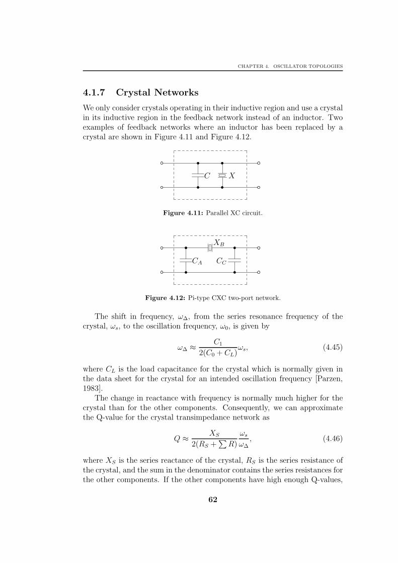
CHAPTER 4. OSCILLATOR TOPOLOGIES
4.1.7 Crystal Networks
We only consider crystals operating in their inductive region and use a crystalin its inductive region in the feedback network instead of an inductor. Twoexamples of feedback networks where an inductor has been replaced by acrystal are shown in Figure 4.11 and Figure 4.12.
C X
Figure 4.11: Parallel XC circuit.
CA
XB
CC
Figure 4.12: Pi-type CXC two-port network.
The shift in frequency, ω∆, from the series resonance frequency of thecrystal, ωs, to the oscillation frequency, ω0, is given by
ω∆ ≈ C1
2(C0 + CL)ωs, (4.45)
where CL is the load capacitance for the crystal which is normally given inthe data sheet for the crystal for an intended oscillation frequency [Parzen,1983].
The change in reactance with frequency is normally much higher for thecrystal than for the other components. Consequently, we can approximatethe Q-value for the crystal transimpedance network as
Q ≈ XS
2(RS +∑R)
ωsω∆
, (4.46)
where XS is the series reactance of the crystal, RS is the series resistance ofthe crystal, and the sum in the denominator contains the series resistances forthe other components. If the other components have high enough Q-values,
62

4.2. ACTIVE NETWORK
the resistive losses are dominated by that of the crystal and the Q-value maybe approximated using (4.9) and (4.7) as
Q ≈ XS
2RS
ωsω∆
≈ QSR1
RS≈ QS
(CL
C0 + CL
)2
, (4.47)
where QS is the series-resonant Q-value of the crystal and we have used
RS ≈ R1
(C0 + CLCL
)2
(4.48)
in the last approximation.The other components have high enough Q-value for the crystal to dom-
inate the total Q-value of the oscillator if
XS∑R
≫ ω∆
ωsQ. (4.49)
In the case when only capacitances are used for the other components, theleft-hand side of the inequality is simply the Q-value for the capacitive reac-tance seen by the crystal.
4.1.8 Frequency Tuning
Frequency tuning is accomplished by introducing electrically adjustable reac-tive components. The most common variable reactances, or simply varactors,are voltage-dependent capacitors, for example MOS varactors or diode var-actors described in Chapter 6. Introducing voltage-dependent capacitors hasthe side-effect of introducing AM-to-PM conversion in the oscillator whichcould increase the phase noise considerably unless measures are taken toprevent this effect. When a large tuning range is sought, we must havean amplitude-regulating mechanism that prevents the AM-to-PM conversionfrom occurring, as discussed in Chapter 5.
Frequency tuning is physically implemented by replacing a capacitanceor part of a capacitance by a varactor, or by placing a varactor in series or inparallel with an inductance in the feedback networks described above. Thefrequency tuning can also be implemented by placing fixed capacitances withseries switches in parallel with the varactors, thereby creating several smallerfrequency tuning ranges that overlap.
4.2 Active Network
The primary task for the active network is to supply the power to keep theoscillations going. The supplied power must balance the power losses in
63
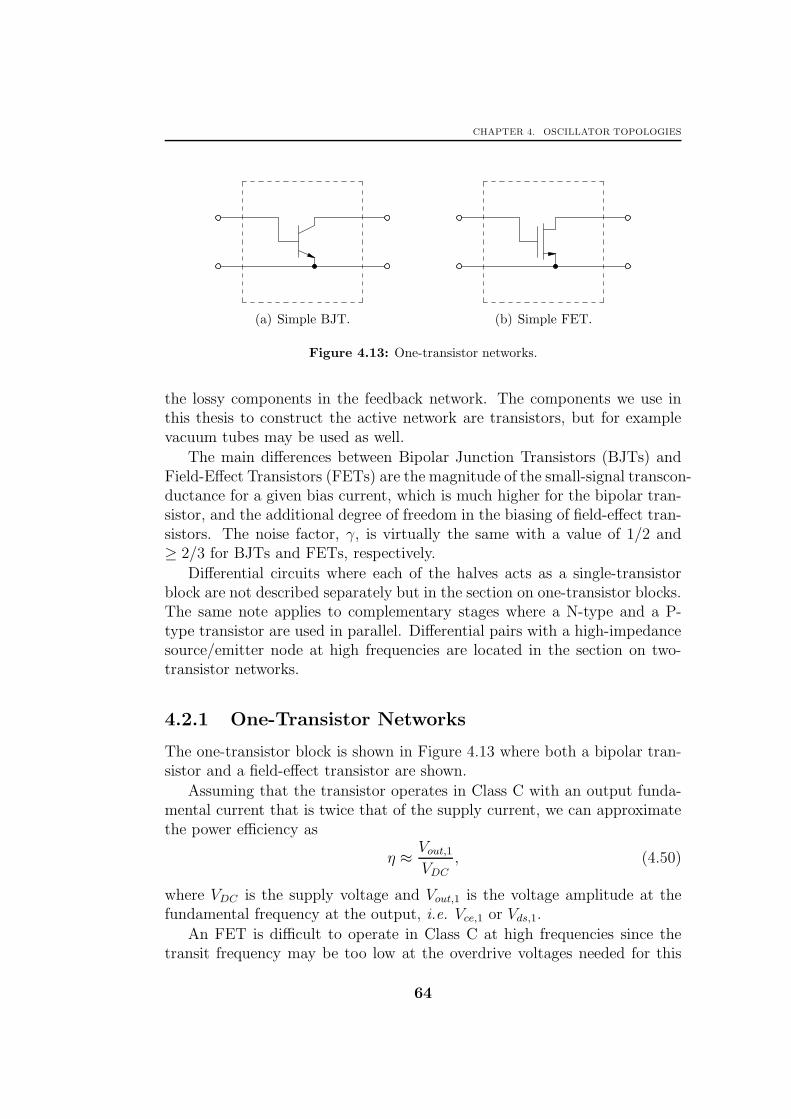
CHAPTER 4. OSCILLATOR TOPOLOGIES
(a) Simple BJT. (b) Simple FET.
Figure 4.13: One-transistor networks.
the lossy components in the feedback network. The components we use inthis thesis to construct the active network are transistors, but for examplevacuum tubes may be used as well.
The main differences between Bipolar Junction Transistors (BJTs) andField-Effect Transistors (FETs) are the magnitude of the small-signal transcon-ductance for a given bias current, which is much higher for the bipolar tran-sistor, and the additional degree of freedom in the biasing of field-effect tran-sistors. The noise factor, γ, is virtually the same with a value of 1/2 and≥ 2/3 for BJTs and FETs, respectively.
Differential circuits where each of the halves acts as a single-transistorblock are not described separately but in the section on one-transistor blocks.The same note applies to complementary stages where a N-type and a P-type transistor are used in parallel. Differential pairs with a high-impedancesource/emitter node at high frequencies are located in the section on two-transistor networks.
4.2.1 One-Transistor Networks
The one-transistor block is shown in Figure 4.13 where both a bipolar tran-sistor and a field-effect transistor are shown.
Assuming that the transistor operates in Class C with an output funda-mental current that is twice that of the supply current, we can approximatethe power efficiency as
η ≈ Vout,1VDC
, (4.50)
where VDC is the supply voltage and Vout,1 is the voltage amplitude at thefundamental frequency at the output, i.e. Vce,1 or Vds,1.
An FET is difficult to operate in Class C at high frequencies since thetransit frequency may be too low at the overdrive voltages needed for this
64

4.2. ACTIVE NETWORK
(a) Differential BJT. (b) Differential FET.
Figure 4.14: Two-transistor networks.
type of operation. Class-A or Class-B operation is often more feasible andthe efficiency becomes
η ≈ KFETVout,1VDC
, (4.51)
where KFET usually has a value in the range 0.5 ∼ 0.8. Higher values arehard to achieve at high operation frequency and low supply voltage, andlower values give too low efficiency.
4.2.2 Two-Transistor Networks
The two-transistor block, the differential pair, is shown in Figure 4.14 whereboth a differential stage based on bipolar transistors and one based on field-effect transistors are included.
Assuming that the differential pair is switching completely, we can ap-proximate the power efficiency as
η ≈ Vout,1πVDC
≤ 2
π(4.52)
where VDC is the supply voltage and Vout,1 is the voltage amplitude at thefundamental frequency at the output and Vout,1 ≤ 2VDC .
4.2.3 Biasing
Biasing provides DC voltage potentials at the terminals of the transistor ordifferential stages. All terminals of the transistor must have a DC potentialin order for the active device to work in a predictable manner. For a bipolartransistor or a discrete FET it implies three potentials and for an integratedFET it implies four potentials that need to be supplied.
Since there are relations between voltages and currents in active devices,we can choose to supply a current instead of a voltage, which in turn decreases
65

CHAPTER 4. OSCILLATOR TOPOLOGIES
the number of potentials to be supplied by one. The current that may besupplied is the source current of an FET or the base or emitter current of aBJT.
Of these different possibilities for biasing the preferred method is to sup-ply gate/base and drain/collector voltage potentials and source/emitter cur-rent. The reason for this choice is that the variation in transconductancewith process and temperature is minimized [Cherry and Hooper, 1968].
Having chosen the type of DC bias, we still need to decouple the DCand AC operation. For AC operation the impedances between the differentnodes should be set by the feedback network alone, and not by the DC biasnetwork. Since we usually want the output of the oscillator to be definedrelative to the supply ground and the feedback networks we consider in thisthesis do not have internal nodes, we signal ground one of the terminals ofthe active block.
Finally, we may need to add components to provide low impedance pathsat higher frequencies to fulfill the filter hypothesis assumed during the deriva-tions of the steady-state operation and the phase noise, that is, that thehigher frequency components are filtered out by the feedback network.
A capacitor may be added when a component having low impedanceat high frequencies and high impedance at low frequencies is needed. Aninductor may be added when a component having high impedance at highfrequencies and low impedance at low frequencies is needed. However, addingextra reactive components may increase the order of the oscillating system,i.e. the number of poles and zeros in the system, making it harder to analyzeand guarantee operation over temperature and process variations. Therefore,it is preferable if the components in the feedback network can act as thebiasing network as well.
Single-Transistor Biasing
For a single transistor, we have that the output voltage must fulfill
vOUT ≥ VOUT,min (4.53)
to stay in its active region of operation. The output voltage, vOUT , is equal tovCE for a BJT and equal to vDS for an FET. The minimum output voltage,VOUT,min, is the saturation voltage, approximately 0.3 V, for a BJT and themaximum overdrive voltage, VGT,max, for an FET.
The maximum input voltage is
max[vIN ] = VIN,max, (4.54)
66

4.2. ACTIVE NETWORK
where the input voltage, vIN , is equal to vBE for a BJT and equal to vGSfor an FET. The maximum input voltage is approximately 0.6∼0.7 V for aBJT and equal to the maximum gate–source voltage for a FET, given byVT + VGT,max, where VT is the threshold voltage of the FET.
Assuming that each of the three nodes has a DC potential plus a funda-mental AC component only, we get
Vb/g,0 − Ve/s,0 + |Vin,1| = VIN,max (4.55)
and
Vc/d,0 − Ve/s,0 − |Vout,1| ≥ VOUT,min, (4.56)
which can be combined to give us
Vc/d,0 − Vb/g,0 − |Vout,1| − |Vin,1| ≥ VOUT,min − VIN,max, (4.57)
where VIN,max−VOUT,min = VT for the FET. This expression can be rewrittento give us an upper limit for the output voltage of
|Vout,1| ≤Vc/d,0 − Vb/g,0 + VIN,max − VOUT,min
1 +∣∣∣Z21
Z11
∣∣∣, (4.58)
where we have used
Vin,1 =Z21
Z11Vout,1 (4.59)
and assumed the fraction of the transimpedances to be real and negative.So far this derivation has been completely general. We now assume that
the transistor is biased with a emitter/source current and that the base/gateand collector/drain terminals each have a fixed DC voltage. The currentsource is assumed to need a voltage drop of at least VBIAS. We investigatethe three cases when one of the three terminals provides a low impedance tosupply ground for AC signals.
We begin with signal-grounding the collector/drain terminal, that is, aCommon Collector (CC) or Common Drain (CD) configuration. The emit-ter/source potential must fulfill
Ve/s,0 ≥ VBIAS + |Vout,1| (4.60)
and consequently from (4.55) and (4.59), we get
Vb/g,0 ≥ |Vout,1|(
1 −∣∣∣∣Z21
Z11
∣∣∣∣)
+ VIN,max + VBIAS. (4.61)
67
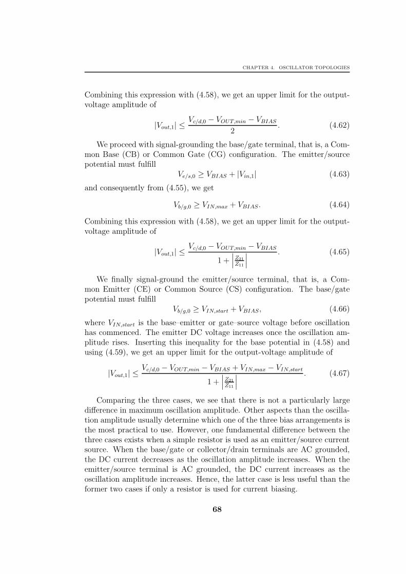
CHAPTER 4. OSCILLATOR TOPOLOGIES
Combining this expression with (4.58), we get an upper limit for the output-voltage amplitude of
|Vout,1| ≤Vc/d,0 − VOUT,min − VBIAS
2. (4.62)
We proceed with signal-grounding the base/gate terminal, that is, a Com-mon Base (CB) or Common Gate (CG) configuration. The emitter/sourcepotential must fulfill
Ve/s,0 ≥ VBIAS + |Vin,1| (4.63)
and consequently from (4.55), we get
Vb/g,0 ≥ VIN,max + VBIAS. (4.64)
Combining this expression with (4.58), we get an upper limit for the output-voltage amplitude of
|Vout,1| ≤Vc/d,0 − VOUT,min − VBIAS
1 +∣∣∣Z21
Z11
∣∣∣. (4.65)
We finally signal-ground the emitter/source terminal, that is, a Com-mon Emitter (CE) or Common Source (CS) configuration. The base/gatepotential must fulfill
Vb/g,0 ≥ VIN,start + VBIAS, (4.66)
where VIN,start is the base–emitter or gate–source voltage before oscillationhas commenced. The emitter DC voltage increases once the oscillation am-plitude rises. Inserting this inequality for the base potential in (4.58) andusing (4.59), we get an upper limit for the output-voltage amplitude of
|Vout,1| ≤Vc/d,0 − VOUT,min − VBIAS + VIN,max − VIN,start
1 +∣∣∣Z21
Z11
∣∣∣. (4.67)
Comparing the three cases, we see that there is not a particularly largedifference in maximum oscillation amplitude. Other aspects than the oscilla-tion amplitude usually determine which one of the three bias arrangements isthe most practical to use. However, one fundamental difference between thethree cases exists when a simple resistor is used as an emitter/source currentsource. When the base/gate or collector/drain terminals are AC grounded,the DC current decreases as the oscillation amplitude increases. When theemitter/source terminal is AC grounded, the DC current increases as theoscillation amplitude increases. Hence, the latter case is less useful than theformer two cases if only a resistor is used for current biasing.
68
4.2. ACTIVE NETWORK
Differential Pair Biasing
A differential pair has a high-impedance middle node. This node is, how-ever, a virtual ground for odd harmonics. The voltage in this node is lowestwhen the differential input is zero. We assume that the input and outputcommon-mode DC voltages are fixed. We treat BJT and FET implementa-tions separately since they behave somewhat differently.
We begin with BJT differential stages. The minimum DC voltage at thebase of the differential pair transistors is given by
Vb,0 ≥ VBIAS + VBE,0, (4.68)
where VBE,0 is the base–emitter voltage of one transistor in the differentialpair when vIN = 0. Since the emitter is at virtual ground for the fundamentalcomponent and we assume that the higher harmonics are filtered out by thefeedback network, we have
vB/G ≈ Vb/g,0 +Vin,1
2cos(ω0t) (4.69)
and
vC/D ≈ Vc/d,0 +Vout,1
2cos(ω0t). (4.70)
For a bipolar transistor, we have the requirement that
vCE = vCB + vBE ≥ VCE,min, (4.71)
where VCE,min is the voltage saturation limit when the base–collector diodebegins to conduct current.
Inserting (4.69) and (4.70) in (4.71) and by using (4.59), we get the max-imum output amplitude as
|Vout,1| ≤2
1 +∣∣∣Z21
Z11
∣∣∣(Vc,0 − VCE,min − Vb,0 + VBE,max), (4.72)
where VBE,max is the base–emitter voltage when one of the transistors con-ducts all of the tail bias current. Using (4.68), we get the maximum outputamplitude as
|Vout,1| ≤2
1 +∣∣∣Z21
Z11
∣∣∣(Vc,0 − VCE,min − VBIAS + VBE,max − VBE,0). (4.73)
For an FET differential pair, the source potential gets pushed down bythe drain potential when the transistor enters its linear region. However,
69

CHAPTER 4. OSCILLATOR TOPOLOGIES
the drain potential must stay somewhat over source potential, which mustat least be VBIAS. Thus, in order for the transistor to conduct the necessarycurrent, we must have
Vd,0 − VDS,min −|Vout,1|
2≥ VBIAS (4.74)
or rewritten as|Vout,1| ≤ 2(Vd,0 − VDS,min − VBIAS), (4.75)
where VDS,min here is the minimum drain–source voltage needed for the tran-sistor to conduct all of the tail current when operating in its linear region.
How to Prevent Common-Mode Oscillations
When implementing differential circuits, we also need to check the common-mode behavior. A simple way to do this is to draw an equivalent common-mode schematic, assuming that the differential and common-mode behaviordoes not affect each other to a high degree. If they do affect each other,which may be the case, the analysis becomes more complicated and this caseis not dealt with here.
We take the differential Colpitts oscillator of Figure 4.15(a) as a first ex-ample. Drawing the equivalent common-mode schematic of Figure 4.15(b),we see that this schematic is also a Colpitts oscillator. If the mutual couplingbetween the two inductors is low, we have a significant common-mode induc-tance and the circuit may have common-mode oscillations, easily checked bycalculating the small-signal loop gain.
By modifying the differential Colpitts oscillator according to Figure 4.16(a),we change the common-mode behavior but not the differential behavior. Wehave replaced the two lower capacitances to ground with a differential capac-itance. We draw the equivalent common-mode schematic in Figure 4.16(b)and see that it is not an oscillator any more for common-mode signals.
How to Prevent Squegging
Even when no explicit amplitude control loop is present, there are still anamplitude control loop present. Since there is a feedback loop present thereis a possibility for instability in the amplitude, often called squegging.
To check if there is any risk for instability in the system, we can calculatethe poles of the system and verify that these are located in the left half-plane. We only check whether the system is stable around the intendedoperating point here, but one should also check the stability of the system
70

4.2. ACTIVE NETWORK
(a) Full schematic. (b) Common mode schematic.
Figure 4.15: Schematic of differential Colpitts oscillator.
(a) Full schematic. (b) Common mode schematic.
Figure 4.16: Schematic of differential Colpitts oscillator.
71

CHAPTER 4. OSCILLATOR TOPOLOGIES
during start-up so the system does reach this operating point without gettinginto trouble.
Since we only consider the system around the operating point, we maylinearize the system. The output currents of the active part are given by
Iout,0(s) = G∆,00Vin,0(s) + G∆,01Vin,1(s) (4.76)
and
Iout,1(s) = G∆,10Vin,0(s) + G∆,11Vin,1(s), (4.77)
where Vin,0 and Vin,1 are the low-frequency input voltage and the input-voltage amplitude, Iout,0 and Iout,1 are the low-frequency output current and
output-current amplitude, and G∆,00, G∆,01, G∆,10 and G∆,11 are the incre-mental large-signal cross-transadmittances of the active part.
Assuming that the feedback network is almost linear, we can write therelationships between input current and output voltage of this network as
Vin,0(s) = H0(s)Iout,0(s) (4.78)
and
Vin,1(s) = H1(s)Iout,1(s) (4.79)
where H0 is the low-frequency transimpedance and H1 is the transfer func-tion for the current amplitude to the voltage amplitude. The low-frequencytransimpedance is given by H0(s) = H(s) in the case of a linear feedbacknetwork. If the feedback transfer function, h, has two conjugate complexpoles near the imaginary axis, we may approximate the transfer function forthe amplitude as
H1(s) ≈H1
1 + s2Qω0
, (4.80)
see also Section 5.5.2. We can now analyze the stability by evaluating thesystem made up by (4.76), (4.77), (4.78) and (4.79).
Squegging is mostly a problem for self-limiting oscillators with low Q-value. It can often be solved by reducing the bias time constant or thecoupling time constant, where the coupling time constant is the most impor-tant one. Other ways to solve the problem could be to increase the Q-valueor decrease the drive voltage for the active element by making |Z21|
Z11lower
[Clarke and Hess, 1971]. The introduction of an explicit control loop for theoscillation amplitude may also solve the problem, see Section 5.5 for furtherdiscussion about Automatic Amplitude Control (AAC).
72

4.2. ACTIVE NETWORK
Start-Up
The start-up of oscillators is a non-trivial problem and is not easy to guar-antee in all cases [Nguyen and Meyer, 1992]. For fairly simple feedback net-works, including parasitic elements, the small-signal gain is a good indicatoras to whether the oscillator could start.
A prerequisite for the oscillator to start is that the small-signal loop gainis larger than unity. Under the assumption that the feedback network islinear, this requirement becomes |Gm| ≥ |G1|, where Gm is the small-signal
transconductance of the active part and G1 is the large-signal transconduc-tance of the active part.
For a BJT single-transistor implementation, we have the small-signaltransconductance as
|Gm| = gm ≈ IC0
VT(4.81)
and the large-signal transconductance as
|G1| =Ic,1Vin,1
=2Ic,0Vin,1
. (4.82)
Assuming that the bias current is equal in both cases, i.e. Ic,0 = IC0, wemust have Vin,1 ≥ 2VT for the oscillator to start.
For an FET single-transistor implementation, we have the small-signaltransconductance as
|Gm| = gm =2ID0
VGT0, (4.83)
assuming the square-law model for the transistor, and the large-signal transcon-ductance as
|G1| =Id,1Vin,1
=2KFETId,0Vin,1
. (4.84)
Assuming that the bias current is equal in both cases, i.e. Id,0 = ID0, wemust have Vin,1 ≥ KFETVGT0 for the oscillator to start.
For a BJT differential pair implementation, we have the small-signaltransconductance as
|Gm| ≈IDC4VT
(4.85)
and the large-signal transconductance as
|G1| =|Iout,1|Vin,1
=2IDCπVin,1
. (4.86)
Assuming that the bias current is equal in both cases, we must have Vin,1 ≥8πVT for the oscillator to start.
73
CHAPTER 4. OSCILLATOR TOPOLOGIES
For an FET differential pair implementation, we have the small-signaltransconductance as
|Gm| ≈IDC
2VGT0(4.87)
and the large-signal transconductance as
|G1| =|Iout,1|Vin,1
=2IDCπVin,1
. (4.88)
Assuming that the bias current is equal in both cases, we must have Vin,1 ≥4πVGT0 for the oscillator to start.
It is sometimes more difficult to guarantee start-up for crystal oscillatorsthan LC oscillators since they may have additional zeros close to the polesin the loop transfer function due to parasitics [Unkrich and Meyer, 1982].
An Automatic Amplitude Control (AAC) may be used when a short start-up time is required since it can give higher small-signal loop gain duringstart-up. This solution is usually used only for crystal oscillators becausethey have much higher Q-values and therefore much longer start-up times.
4.3 Noise from Bias Current Source
In this section, we calculate the noise contributions from simple currentsources implemented with transistors. The schematics for these currentsources are shown in Figure 4.17, both for implementations with a BJT andwith an FET. The voltage source VB or VG may be another transistor imple-mentation, as is the case when the current source is part of a current mirror,or it could be a constant voltage generator or a variable voltage, which maybe the case when implementing an Automatic Amplitude Control (AAC). Inany case, the bias voltage may also contribute noise which must be accountedfor, but here we only consider noise coming from the transistor and from theresistor RE or RS.
4.3.1 White Noise from Bias Current Source
Assuming that the input noise and noise from RB and RG are negligible, wehave the noise spectral density as
Sb ≈ 4kBT1
RE/S(4.89)
when gmRE/S ≫ 1, where gm is the transconductance of the transistor and
Sb ≈ 4kBTγgm (4.90)
74

4.3. NOISE FROM BIAS CURRENT SOURCE
IDC
RB
REVB
(a) BJT current source.
IDC
RS
RG
VG
(b) FET current source.
Figure 4.17: Implementations of current source.
when RE or RS is negligible, and where γ is approximately 2/3 for FETs and1/2 for BJTs.
4.3.2 1/f Noise from Bias Current Source
The bias current source may contribute with a significant amount of 1/fnoise, which may be up-converted to phase noise. In this section, we calculatethe noise spectral density for this 1/f noise contribution. We assume thata bias current implemented as a resistor only contributes an insignificantamount of 1/f noise, and we hence concentrate on implementations containingtransistors.
BJT
For a bipolar transistor, the 1/f noise current source is located between thebase and the emitter with a spectral density given in (C.18) of Appendix Cas
i2b =K1/f
fIB ≈ K1/f
f
IDCβ, (4.91)
where K1/f is a noise constant, IB is the base current, IDC is the bias current,and β is the current amplification factor of the transistor.
We now have the 1/f noise from the bias current source as
Sb(f) ≈(
gmRB + gmRE
1 + gmRE + gmRB1β
)2K1/f
f
IDCβ, (4.92)
assuming that β ≫ 1, and where gm is the transconductance of the transistor.
75

CHAPTER 4. OSCILLATOR TOPOLOGIES
Writing this expression as
Sb(f) =K1/f,bIDC
f(4.93)
gives the constant K1/f,b as
K1/f,b ≈(
gmRB + gmRE
1 + gmRE + gmRB1β
)2K1/f
β. (4.94)
Since the resistance of RB usually is non-negligible and we have inserted aresistor RE , we have
K1/f
β< K1/f,b < βK1/f . (4.95)
FET
For an FET, the 1/f noise current source is located between the drain andthe source with a spectral density given in (C.32) of Appendix C as
i2d =K1/f
fIDC , (4.96)
where K1/f is a noise constant and IDC is the bias source current.We now have the 1/f noise from the bias current source as
Sb(f) =
(1
1 + gmRS
)2 K1/f
fIDC , (4.97)
where gm is the transconductance of the transistor. Writing this expressionas
Sb(f) =K1/f,bIDC
f, (4.98)
we get the constant K1/f,b as
K1/f,b =
(1
1 + gmRS
)2
K1/f . (4.99)
If RS is not present, we get
K1/f,b = K1/f (4.100)
and if gmRS ≫ 1, we get
K1/f,b ≈K1/f
g2mR
2S
. (4.101)
76

4.4. PHASE-NOISE PERFORMANCE
4.4 Phase-Noise Performance
To determine which bias arrangement gives the lowest phase noise due towhite noise in the components, we evaluate the maximum achievable Oscil-lator Design Efficiency (ODE), Υ, derived in Section 3.2.1 to be
Υ =η
F, (4.102)
where η is the power efficiency and F is the noise factor. We evaluate theODE both for oscillators based on FETs and for oscillators based on BJTs.Oscillators using both types of transistors are not considered here, but couldeasily be evaluated using the same method.
In this section, we assume that the Z-parameters are real in order tosimplify the expressions. We further note that Z11 and Z22 must be positivesince the input and output resistances for a passive network are positive.
4.4.1 FET
The minimum voltage needed for the operation of the bias current generatorof Section 4.3 is given by
VBIAS = VGT , (4.103)
where VGT is the overdrive voltage of the bias transistor, and where we haveassumed that RS = 0. The approximate noise spectral density of the biascurrent generator is given in (4.90) as
Sb ≈ 4kBTγgm,b, (4.104)
where the transconductance of the transistor, gm,b, is given by
gm,b =2IDCVGT
, (4.105)
where IDC is the bias current, and where we have assumed that the transistorcan be described by the square-law model.
The output-voltage amplitude of the active part is given by
Vout,1 = Z11Iout,1, (4.106)
where the output-current amplitude, Iout,1, for a single transistor is approxi-mately given by
|Iout,1| ≈ 2KFETIDC , (4.107)
77

CHAPTER 4. OSCILLATOR TOPOLOGIES
where KFET is defined in Section 4.2.1. Hence, we get the minimum voltageneeded for the current bias generator as
VBIAS ≈ 1
KFETgm,bZ11
Vout,1 (4.108)
by combining (4.103), (4.105), (4.106) and (4.107).For a differential pair, the output-current amplitude is approximately
given as
|Iout,1| ≈2
πIDC (4.109)
when the differential pair is completely switching. Consequently, the mini-mum voltage needed for the bias current generator is given by
VBIAS ≈ π
gm,bZ11|Vout,1|. (4.110)
For an oscillator based on a single FET, we have the approximate powerefficiency from (4.51) as
η ≈ KFET|Vout,1|VDC
, (4.111)
where KFET has a value less than unity.For an oscillator based on FETs operating as a differential stage, the
approximate power efficiency is given by (4.52) as
η ≈ |Vout,1|πVDC
. (4.112)
The noise factor of oscillators where the AM-to-PM conversion is negli-gible is given in Section 7.2.6 as
F ≈ 1 + γZ11
|Z21|+K1K2, (4.113)
whereK1 = γgm,bZ11 (4.114)
and
K2 =
2Kim ≤ 14
differential pair tail bias1 bias at outputZ2
22
Z221
bias at input(4.115)
We assume below that Kim ≈ 18
and that
Z222
Z221
≈ Z221
Z211
, (4.116)
which is the case for an oscillator designed to have low phase noise due towhite noise.
78

4.4. PHASE-NOISE PERFORMANCE
Signal-Grounded Drain
For a signal-grounded drain, also termed Common Drain (CD), we have themaximum output-voltage amplitude from (4.62) as
|Vout,1| ≈Vd,0 − VDS,min − VBIAS
2. (4.117)
Inserting the expression for minimum voltage for supply current biasing in(4.108), we get the maximum output-voltage amplitude as
|Vout,1| ≈Vd,0 − VDS,min
2 + 1KF ET
1gm,bZ11
. (4.118)
Inserting this expression in (4.111), we get the power efficiency as
η ≈ KFET (Vd,0 − VDS,min)
VDC
(2 + 1
KF ET
1gm,bZ11
) . (4.119)
The noise factor for a signal-grounded drain is given from (4.113) as
F ≈ 1 + γZ11
|Z21|+ γgm,bZ11. (4.120)
Inserting the expression for the power efficiency and the expression for thenoise factor in (4.102), we get the oscillator design efficiency as
Υ ≈ KFET (Vd,0 − VDS,min)
VDC
(2 + 1
KF ET
1gm,bZ11
)(1 + γ Z11
|Z21| + γgm,bZ11
) , (4.121)
which can be rewritten as
Υ ≈ Vd,0 − VDS,minVDC
Υnorm, (4.122)
where
Υnorm =KFET(
2 + 1KF ET
1gm,bZ11
)(1 + γ Z11
|Z21| + γgm,bZ11
) (4.123)
is the oscillator design efficiency we would get if the overdrive voltages ofthe transistors in the active part were negligible compared to the supplyvoltage and the drain potential is equal to the supply voltage. This ODE isplotted in Figure 4.18(a) for γ = 1 with KFET = 0.6 as function of Z11
|Z21| with
gm,bZ11 = 1.29 and as function of gm,bZ11 with Z11
|Z21| = 1.
79

CHAPTER 4. OSCILLATOR TOPOLOGIES
Signal-Grounded Gate
For a signal-grounded gate, also termed Common Gate (CG), we have themaximum output-voltage amplitude from (4.65) as
|Vout,1| ≈Vd,0 − VDS,min − VBIAS
1 + |Z21|Z11
. (4.124)
Inserting the expression for minimum voltage for supply current biasing in(4.108), we get the maximum output-voltage amplitude as
|Vout,1| ≈Vd,0 − VDS,min
1 + |Z21|Z11
+ 1KF ET
1gm,bZ11
. (4.125)
Inserting this expression in (4.111), we get the power efficiency as
η ≈ KFET (Vd,0 − VDS,min)
VDC
(1 + |Z21|
Z11+ 1
KF ET
1gm,bZ11
) . (4.126)
The noise factor for a signal-grounded gate is given from (4.113) as
F ≈ 1 + γZ11
|Z21|+Z2
21
Z211
γgm,bZ11. (4.127)
Inserting the expression for the power efficiency and the expression for thenoise factor in (4.102), we get the oscillator design efficiency as
Υ ≈ KFET (Vd,0 − VDS,min)
VDC
(1 + |Z21|
Z11+ 1
KF ET
1gm,bZ11
)(1 + γ Z11
|Z21| +Z2
21
Z211γgm,bZ11
) , (4.128)
which can be rewritten as
Υ ≈ Vd,0 − VDS,minVDC
Υnorm, (4.129)
where
Υnorm =KFET(
1 + |Z21|Z11
+ 1KF ET
1gm,bZ11
)(1 + γ Z11
|Z21| +Z2
21
Z211γgm,bZ11
) (4.130)
is the oscillator design efficiency we would get if the overdrive voltages ofthe transistors in the active part were negligible compared to the supplyvoltage and the drain potential is equal to the supply voltage. This ODE isplotted in Figure 4.18(b) for γ = 1 with KFET = 0.6 as function of Z11
|Z21| with
gm,bZ11 = 2.60 and as function of gm,bZ11 with Z11
|Z21| = 5.42.
80

4.4. PHASE-NOISE PERFORMANCE
Signal-Grounded Source
For a signal-grounded source, also termed Common Source (CS), we havethe maximum output-voltage amplitude from (4.67) as
|Vout,1| ≈Vd,0 − VDS,min − VBIAS + VGS,max − VGS,start
1 + |Z21|Z11
. (4.131)
Since the noise source is short-circuited through the signal ground at thesource terminal, there is no trade-off between noise and voltage drop overthe bias current generator. Inserting this expression in (4.111), we get thepower efficiency as
η ≈ KFET (Vd,0 − VDS,min − VBIAS + VGS,max − VGS,start)
VDC
(1 + |Z21|
Z11
) . (4.132)
The noise factor for a signal-grounded source is given from (4.113) as
F ≈ 1 + γZ11
|Z21|. (4.133)
Inserting the expression for the power efficiency and the expression for thenoise factor in (4.102), we get the oscillator design efficiency as
Υ ≈ KFET (Vd,0 − VDS,min − VBIAS + VGS,max − VGS,start)
VDC
(1 + |Z21|
Z11
)(1 + γ Z11
|Z21|
) , (4.134)
which can be rewritten as
Υ ≈ Vd,0 − VDS,min − VBIAS + VGS,max − VGS,startVDC
Υnorm, (4.135)
where
Υnorm =KFET(
1 + |Z21|Z11
)(1 + γ Z11
|Z21|
) (4.136)
is the oscillator design efficiency we would get if the overdrive voltages of thetransistors in the active part were negligible compared to the supply voltageand the drain potential is equal to the supply voltage. This ODE is plottedin Figure 4.18(c) for γ = 1 with KFET = 0.6 as function of Z11
|Z21| . We have
the maximum ODE when Z11
|Z21| = 1.
81

CHAPTER 4. OSCILLATOR TOPOLOGIES
Differential Pair
For a differential pair, we have the maximum output-voltage amplitude from(4.75) as
|Vout,1| ≈ 2(Vd,0 − VDS,min − VBIAS). (4.137)
Inserting the expression for minimum voltage for supply current biasing in(4.110), we get the maximum output-voltage amplitude as
|Vout,1| ≈2(Vd,0 − VDS,min)
1 + 2π 1gm,bZ11
. (4.138)
Inserting this expression in (4.112), we get the power efficiency as
η ≈ 2(Vd,0 − VDS,min)
πVDC
(1 + 2π 1
gm,bZ11
) . (4.139)
The noise factor for a differential stage is given from (4.113) as
F ≈ 1 + γZ11
|Z21|+
1
4γgm,bZ11. (4.140)
Inserting the expression for the power efficiency and the expression for thenoise factor in (4.102), we get the oscillator design efficiency as
Υ ≈ 2(Vd,0 − VDS,min)
πVDC
(1 + 2π 1
gm,bZ11
)(1 + γ Z11
|Z21| + 14γgm,bZ11
) , (4.141)
which can be rewritten as
Υ ≈ Vd,0 − VDS,minVDC
Υnorm, (4.142)
where
Υnorm =2
π(1 + 2π 1
gm,bZ11
)(1 + γ Z11
|Z21| + 14γgm,bZ11
) (4.143)
is the oscillator design efficiency we would get if the overdrive voltages of thetransistors in the active part were negligible compared to the supply voltageand the drain potential is equal to the supply voltage. This ODE is plottedin Figure 4.18(d) for γ = 1 as function of Z11
|Z21| with gm,bZ11 = 7.09 and as
function of gm,bZ11 with Z11
|Z21| = 1.
82

4.4. PHASE-NOISE PERFORMANCE
0 1 2 3 4 5 6 7 8 9 10−19
−18
−17
−16
−15
−14
−13
−12
−11
FET, Signal−grounded drain, KFET
=0.6, γ=1
Z11
/|Z21
| , gm,b
Z11
ϒ norm
[dB
]
ϒnorm
(Z11
/|Z21
|)ϒ
norm(g
m,bZ
11)
(a) Signal-grounded drain.
0 1 2 3 4 5 6 7 8 9 10−20
−18
−16
−14
−12
−10
−8
FET, Signal−grounded gate, KFET
=0.6, γ=1
Z11
/|Z21
| , gm,b
Z11
ϒ norm
[dB
]
ϒnorm
(Z11
/|Z21
|)ϒ
norm(g
m,bZ
11)
(b) Signal-grounded gate.
0 1 2 3 4 5 6 7 8 9 10−14
−13
−12
−11
−10
−9
−8
FET, Signal−grounded source, KFET
=0.6, γ=1
Z11
/|Z21
|
ϒ norm
[dB
]
(c) Signal-grounded source.
0 1 2 3 4 5 6 7 8 9 10−17
−16
−15
−14
−13
−12
−11
−10
−9FET, Differential pair, γ=1
Z11
/|Z21
| , gm,b
Z11
ϒ norm
[dB
]
ϒnorm
(Z11
/|Z21
|)ϒ
norm(g
m,bZ
11)
(d) Differential stage.
Figure 4.18: Oscillator design efficiency for FET active network.
83

CHAPTER 4. OSCILLATOR TOPOLOGIES
4.4.2 BJT
The minimum voltage needed for the bias current generator of Section 4.3 isgiven by
VBIAS = REIDC + VCE,min, (4.144)
where VCE,min is the minimum collector-emitter voltage needed for operationin the active region of the transistor. The approximate noise spectral densityof the bias current generator is given in (4.89) as
Sb ≈ 4kBT1
RE. (4.145)
The output-voltage amplitude of the active part is given by
Vout,1 = Z11Iout,1, (4.146)
where the output current, Iout,1, for a transistor operating in Class C is givenby
|Iout,1| ≈ 2IDC . (4.147)
Consequently, the minimum voltage needed for the current bias generator isgiven by
VBIAS ≈ RE
2Z11|Vout,1| + VCE,min, (4.148)
by combining (4.144), (4.146) and (4.147).For a differential pair, the output current is approximately given as
|Iout,1| ≈2
πIDC (4.149)
when the differential pair is completely switching. Hence, the minimumvoltage needed for the bias current generator is given by
VBIAS ≈ πRE
2Z11|Vout,1| + VCE,min. (4.150)
For an oscillator based on a single BJT, we have the approximate powerefficiency from (4.50) as
η ≈ |Vout,1|VDC
. (4.151)
For an oscillator based on BJTs operating as a differential stage, theapproximate power efficiency is given by (4.52) as
η ≈ |Vout,1|πVDC
. (4.152)
84
4.4. PHASE-NOISE PERFORMANCE
The noise factor of oscillators where the AM-to-PM conversion is negli-gible is given in Section 7.2.6 as
F ≈ 1 +1
2
Z11
|Z21|+K1K2, (4.153)
where
K1 =Z11
RE
(4.154)
and
K2 =
2Kim ≤ 14
differential pair tail bias1 bias at outputZ2
22
Z221
bias at input(4.155)
We assume below that Kim ≈ 18
and that
Z222
Z221
≈ Z221
Z211
, (4.156)
which is the case for an oscillator designed to have low phase noise due towhite noise.
Signal-Grounded Collector
For a signal-grounded collector, also termed Common Collector (CC), wehave the maximum output-voltage amplitude from (4.62) as
|Vout,1| ≈Vc,0 − VCE,min − VBIAS
2. (4.157)
Inserting the expression for minimum voltage for supply current biasing in(4.148), we get the maximum output-voltage amplitude as
|Vout,1| ≈Vc,0 − VCE,min − VCE,min
2 + 12RE
Z11
. (4.158)
Inserting this expression in (4.151), we get the power efficiency as
η ≈ (Vc,0 − VCE,min − VCE,min)
VDC
(2 + 1
2RE
Z11
) . (4.159)
The noise factor for a signal-grounded collector is given from (4.153) as
F ≈ 1 +1
2
Z11
|Z21|+Z11
RE
. (4.160)
85

CHAPTER 4. OSCILLATOR TOPOLOGIES
Inserting the expression for the power efficiency and the expression for thenoise factor in (4.102), we get the oscillator design efficiency as
Υ ≈ (Vc,0 − VCE,min − VCE,min)
VDC
(2 + 1
2RE
Z11
)(1 + 1
2Z11
|Z21| + Z11
RE
) , (4.161)
which can be rewritten as
Υ ≈ Vc,0 − VCE,min − VCE,minVDC
Υnorm, (4.162)
where
Υnorm =1(
2 + 12RE
Z11
)(1 + 1
2Z11
|Z21| + Z11
RE
) (4.163)
is the oscillator design efficiency we would get if the saturation voltages of thetransistors were negligible compared to the supply voltage and the collectorpotential is equal to the supply voltage. This ODE is plotted in Figure 4.19(a)as function of Z11
|Z21| with Z11
RE= 0.61 and as function of Z11
REwith Z11
|Z21| = 1.
Signal-Grounded Base
For a signal-grounded base, also termed Common Base (CB), we have themaximum output-voltage amplitude from (4.65) as
|Vout,1| ≈Vc,0 − VCE,min − VBIAS
1 + |Z21|Z11
. (4.164)
Inserting the expression for minimum voltage for supply current biasing in(4.148), we get the maximum output-voltage amplitude as
|Vout,1| ≈Vc,0 − VCE,min − VCE,min
1 + |Z21|Z11
+ 12RE
Z11
. (4.165)
Inserting this expression in (4.151), we get the power efficiency as
η ≈ (Vc,0 − VCE,min − VCE,min)
VDC
(1 + |Z21|
Z11+ 1
2RE
Z11
) . (4.166)
The noise factor for a signal-grounded base is given from (4.153) as
F ≈ 1 +1
2
Z11
|Z21|+Z2
21
Z211
Z11
RE
. (4.167)
86

4.4. PHASE-NOISE PERFORMANCE
Inserting the expression for the power efficiency and the expression for thenoise factor in (4.102), we get the oscillator design efficiency as
Υ ≈ (Vc,0 − VCE,min − VCE,min)
VDC
(1 + |Z21|
Z11+ 1
2RE
Z11
)(1 + 1
2Z11
|Z21| +Z2
21
Z211
Z11
RE
) , (4.168)
which can be rewritten as
Υ ≈ Vc,0 − VCE,min − VCE,minVDC
Υnorm, (4.169)
where
Υnorm =1(
1 + |Z21|Z11
+ 12RE
Z11
)(1 + 1
2Z11
|Z21| +Z2
21
Z211
Z11
RE
) (4.170)
is the oscillator design efficiency we would get if the saturation voltagesof the transistors were negligible compared to the supply voltage and thecollector potential is equal to the supply voltage. This ODE is plotted inFigure 4.19(b) as function of Z11
|Z21| with Z11
RE= 2.44 and as function of Z11
RE
with Z11
|Z21| = 2.66.
Signal-Grounded Emitter
For a signal-grounded emitter, also termed Common Emitter (CE), we havethe maximum output-voltage amplitude from (4.67) as
|Vout,1| ≈Vc,0 − VCE,min − VBIAS + VBE,max − VBE,start
1 + |Z21|Z11
. (4.171)
Since the noise source is short-circuited through the signal ground at theemitter terminal, there is no trade-off between noise and voltage drop overthe bias current generator. Inserting this expression in (4.151), we get thepower efficiency as
η ≈ (Vc,0 − VCE,min − VBIAS + VBE,max − VBE,start)
VDC
(1 + |Z21|
Z11
) . (4.172)
The noise factor for a signal-grounded emitter is given from (4.153) as
F ≈ 1 +1
2
Z11
|Z21|. (4.173)
87

CHAPTER 4. OSCILLATOR TOPOLOGIES
Inserting the expression for the power efficiency and the expression for thenoise factor in (4.102), we get the oscillator design efficiency as
Υ ≈ (Vc,0 − VCE,min − VBIAS + VBE,max − VBE,start)
VDC
(1 + |Z21|
Z11
)(1 + 1
2Z11
|Z21|
) , (4.174)
which can be rewritten as
Υ ≈ Vc,0 − VCE,min − VBIAS + VBE,max − VBE,startVDC
Υnorm, (4.175)
where
Υnorm =1(
1 + |Z21|Z11
)(1 + γ Z11
|Z21|
) (4.176)
is the oscillator design efficiency we would get if the saturation voltages of thetransistors were negligible compared to the supply voltage and the collectorpotential is equal to the supply voltage. This ODE is plotted in Figure 4.19(c)as function of Z11
|Z21| . The maximum ODE is achieved when Z11
|Z21| = 1.41.
Differential Pair
For a differential pair, we have the maximum output-voltage amplitude from(4.73) as
|Vout,1| ≈2(Vc,0 − VCE,min − VBIAS + VBE,max − VBE,0)
1 + |Z21|Z11
. (4.177)
Inserting the expression for minimum voltage for supply current biasing in(4.150), we get the maximum output-voltage amplitude as
|Vout,1| ≈2(Vc,0 − VCE,min − VCE,min + VBE,max − VBE,0)
1 + |Z21|Z11
+ π RE
Z11
. (4.178)
Inserting this expression in (4.152), we get the power efficiency as
η ≈ 2(Vc,0 − VCE,min − VCE,min + VBE,max − VBE,0)
πVDC
(1 + |Z21|
Z11+ π RE
Z11
) . (4.179)
The noise factor for a differential stage is given from (4.153) as
F ≈ 1 +1
2
Z11
|Z21|+
1
4
Z11
RE
. (4.180)
88

4.4. PHASE-NOISE PERFORMANCE
Inserting the expression for the power efficiency and the expression for thenoise factor in (4.102), we get the oscillator design efficiency as
Υ ≈ 2(Vc,0 − VCE,min − VCE,min + VBE,max − VBE,0)
πVDC
(1 + |Z21|
Z11+ π RE
Z11
)(1 + 1
2Z11
|Z21| + 14Z11
RE
) , (4.181)
which can be rewritten as
Υ ≈ (Vc,0 − VCE,min − VCE,min + VBE,max − VBE,0)
VDCΥnorm, (4.182)
where
Υnorm =2
π(1 + |Z21|
Z11+ π RE
Z11
)(1 + 1
2Z11
|Z21| + 14Z11
RE
) (4.183)
is the oscillator design efficiency we would get if the saturation voltagesof the transistors were negligible compared to the supply voltage and thecollector potential is equal to the supply voltage. This ODE is plotted inFigure 4.19(d) as function of Z11
|Z21| with Z11
RE= 3.54 and as function of Z11
RE
with Z11
|Z21| = 1.41.
4.4.3 Summary
The maximum values for the ODE Υnorm are summarized in Table 4.2 fordifferent biasing options. For the FET, we assume that KFET = 0.6 andγ = 1. In all cases, we assume that there is no filtering of noise coming fromthe biasing transistor. We also assume that Z11
|Z21| ≥ 1 and that the currentsource gives a constant current during the entire oscillation period.
Table 4.2: Summary of optimum phase noise.
Signal-grounded FET [dB] BJT [dB]
Drain/Collector −12.6 −7.7Gate/Base −8.7 −6.3Source/Emitter −8.2 −4.6Differential stage −10.5 −10.2
89

CHAPTER 4. OSCILLATOR TOPOLOGIES
0.5 1 1.5 2 2.5 3 3.5 4 4.5 5−11.5
−11
−10.5
−10
−9.5
−9
−8.5
−8
−7.5
−7BJT, Signal−grounded collector
Z11
/|Z21
| , Z11
/RE
ϒ norm
[dB
]
ϒnorm
(Z11
/|Z21
|)ϒ
norm(Z
11/R
E)
(a) Signal-grounded collector.
0.5 1 1.5 2 2.5 3 3.5 4 4.5 5−16
−15
−14
−13
−12
−11
−10
−9
−8
−7
−6BJT, Signal−grounded base
Z11
/|Z21
| , Z11
/RE
ϒ norm
[dB
]
ϒnorm
(Z11
/|Z21
|)ϒ
norm(Z
11/R
E)
(b) Signal-grounded base.
0.5 1 1.5 2 2.5 3 3.5 4 4.5 5−6.4
−6.2
−6
−5.8
−5.6
−5.4
−5.2
−5
−4.8
−4.6BJT, Signal−grounded emitter
Z11
/|Z21
|
ϒ norm
[dB
]
(c) Signal-grounded emitter.
0.5 1 1.5 2 2.5 3 3.5 4 4.5 5−14
−13.5
−13
−12.5
−12
−11.5
−11
−10.5
−10BJT, Differential pair
Z11
/|Z21
| , Z11
/RE
ϒ norm
[dB
]
ϒnorm
(Z11
/|Z21
|)ϒ
norm(Z
11/R
E)
(d) Differential stage.
Figure 4.19: Oscillator design efficiency for BJT active network.
90
Chapter 5Amplitude Control
M ost practical oscillators employ some type of amplitude control tokeep the oscillation voltage amplitude constant over manufacturingvariations, temperature variations, and aging. This chapter describes
various techniques to achieve such amplitude control and their characteristics,such as their impact on phase noise.
5.1 Introduction
The different amplitude controls can be grouped into the four categories listedbelow:
• Temperature-sensitive resistor
• Diode clamping
• Nonlinearity in the active network
• Automatic amplitude control
The former two methods affect the feedback network; they lower the os-cillation amplitude by introducing additional losses in order to bring theamplitude down to a predefined value. The latter two methods lower theoutput current from the active part when the oscillation amplitude exceedsthe predefined value. The first and last methods use a dynamic nonlinearitywhile the other methods use a static nonlinearity to control the oscillationamplitude.
We assume the feedback network to be designed such that a limitationof the voltage amplitude between two nodes will limit the voltage amplitude
91

CHAPTER 5. AMPLITUDE CONTROL
between any two nodes. This assumption implies that the transimpedance,Z21, of the feedback network must be proportional to its input impedance,Z11. We also assume that the input impedance to the feedback network, Z11,is resistive and proportional to the Q-value of the feedback network.
From Chapter 7 we have the phase noise at a frequency offset, ωm, dueto white noise sources as
L[ωm] ≈ kBTFZ11
V 2out,1Q
2
ω20
ω2m
, (5.1)
where kB is the Boltzmann constant, T is the temperature, Q is the Q-valueof the oscillator, ω0 is the oscillation frequency, Vout,1 is the voltage amplitudeat the output of the active part, and F is the noise factor given by
F ≈ 1 + γZ11
|Z21|+K1K2 +K2
AM−PM
(1 + γ|G(I)
∆,1|Z11 +K1K3
), (5.2)
where KAM−PM is the AM-to-PM conversion, Z11 and Z21 are the inputimpedance and transimpedance of the feedback network at the oscillationfrequency, G
(I)∆,1 is the incremental large-signal transconductance of the am-
plifying part of the active part, γ is a noise constant depending on the tran-sistor type used, and K1, K2 and K3 are bias-dependent expressions given inSection 7.2.6.
As derived in Section 8.4, we have the AM-to-PM conversion as
KAM−PM =|Y1|H(I)
∆,1
(∂α∂|X1| + ∂ζ
∂|X1|
)
1 − F(I)∆,1H
(I)∆,1
, (5.3)
where Y1 is the fundamental output-current amplitude of the active part, X1
is the fundamental input-voltage amplitude to the active part, α and ζ arethe phase shifts of the feedback and active parts, respectively, and F
(I)∆,1 and
H(I)∆,1 are the incremental large-signal gains of the active network and of the
feedback network, respectively.The parts of the expression for the phase noise mainly affected by the
amplitude control are Q, Z11, Z21, F(I)∆,1 and H
(I)∆,1. The remainder of this
chapter is dedicated to the four methods of amplitude control and theirimpact on these parts.
5.2 Limiting Using Temperature-Sensitive Re-
sistor
A temperature-sensitive resistor is a component with a resistance that in-creases or decreases with temperature. The power loss in this component
92
5.3. DIODE LIMITING
will increase its own temperature which in turn increases or decreases the re-sistance and lowers the oscillation amplitude by introducing additional losses.The change in resistance is determined by the average power loss with a timedelay equal to the thermal time constant. Hence, the nonlinearity is dynamicand not static.
The relatively high thermal time constant for such a component meansthat it cannot keep up with fast amplitude variations, which in turn meansthat it does not decrease the AM-to-PM conversion. However, the resistormight be very linear and as such could be used when high spectral purity isneeded, i.e., when low power at higher harmonics is sought.
For this type of limiting we have that H(I)∆,1 ≈ H1, F
(I)∆,1 is not affected,
and Q and Z11 are lowered to bring the oscillation amplitude down.An example of an implementation of a self-regulating temperature-sensitive
resistor is a light bulb. The resistance of the filament increases with its owntemperature.
5.2.1 Phase-Noise Contribution
The single-sided current-noise spectral density of the temperature-sensitiveresistor is simply
i2 = 4kBTRR, (5.4)
where R is the resistance and TR is the operating temperature of the resistor.In addition to the increase in phase noise due to the decrease in the Q-
value, we have inserted a noisy component operating at a higher temperatureand consequently contributing extra noise. If the Q-value of the feedback net-work is dominated by the temperature-sensitive resistor, we can approximatethe noise factor as
F ≈ TRT
+ γZ11
|Z21|+K1K2 +K2
AM−PM
(TRT
+ γ|G(I)∆,1|Z11 +K1K3
), (5.5)
where T is the temperature of the oscillator, excluding the temperature-sensitive resistor.
5.3 Diode Limiting
By inserting a diode between two nodes in the feedback network, we limitthe voltage amplitude between these two nodes. A diode has an exponen-tial relationship between voltage and current. Hence, an increase in currentthrough the diode will only increase the voltage over the diode by a small
93

CHAPTER 5. AMPLITUDE CONTROL
amount. The diode is a static nonlinearity reacting momentarily to a changein voltage amplitude.
Diode limiting makes H∆,1 ≪ H1. Consequently, the upconversion ofwhite noise to phase noise due to the AM-to-PM conversion diminishes. Theincremental large-signal gain in the active part, F
(I)∆,1, is not affected since
the diode is inserted in the feedback network, and Q and Z11 are lowered tobring the oscillation amplitude down.
When diodes are inserted in the feedback network, we call it explicit diodelimiting, and when the inherent diode of a bipolar transistor is used, we call itbase–collector diode limiting. The base–collector diode limiting works in thesame way as the explicit diode limiting, but uses the inherent base–collectordiode of the bipolar transistor. Hence, the voltage swing between collectorand base is limited such that the collector potential is not lower than onebuilt-in diode potential below the base potential, where the built-in potentialfor a silicon diode is approximately 0.6∼0.7 V in room temperature.
Often diodes conducting currents in different directions are connected inparallel when a fully differential solution is designed. Otherwise, a directcurrent will flow between the two nodes preventing the nodes to act fullydifferentially.
5.3.1 Phase-Noise Contribution
From Section 7.2.4, we have that the phase-noise contribution of a diode ishalf that of the corresponding resistor with equal large-signal conductance.Hence, we approximate the noise factor, F , as
F ≈ KD + γZ11
|Z21|+K1K2, (5.6)
where KD ranges from unity when the diode limiting does not affect theQ-value to 1/2 when the Q-value is dominated by the amplitude limitingdiodes.
The diode limiting affects the phase noise in several ways: by loweringthe Q-value and the input impedance of the feedback network, and by itsown contribution to the phase noise. The total phase noise may, however,decrease compared to the case without the amplitude regulation since theAM-to-PM conversion decreases.
94

5.4. LIMITING USING NONLINEARITY IN THE ACTIVE NETWORK
5.4 Limiting Using Nonlinearity in the Ac-
tive Network
The nonlinearity of the active component we discuss in this section is thelinear region of the field-effect transistor. Inherent limiting in bipolar tran-sistors is discussed in Section 5.3.
The type of limiting discussed in this section makes H∆,1 ≪ H1 in a waysimilar to that of diode limiting. Consequently, the upconversion of whitenoise to phase noise due to the AM-to-PM conversion diminishes. However,the limiting using the linear region of FETs is not as strong as that of diodelimiting since the I–V characteristics is less nonlinear. We also have that F
(I)∆,1
is not affected, and Q and Z11 are lowered to bring the oscillation amplitudedown.
5.4.1 Phase-Noise Contribution
When the drain potential comes close to that of the source terminal, thetransistor enters its linear region and the drain current decreases. However,the spectral density of the drain-current noise does not decrease when thetransistor enters the linear region as discussed in Appendix C.3. Assumingthat the noise constant of the transistor, γ, is equal in the active and linearregions, we get the approximate noise factor as
F ≈ 1 + γZ11
|Z21|+K1K2, (5.7)
assuming that the limiting is strong enough to make the phase-noise contri-bution from the AM-to-PM conversion negligible.
5.4.2 Differential Pair Current Source
Another way of achieving amplitude limiting using the active componentoccurs when the voltage headroom for the current source goes down for partof the oscillation period, thus decreasing the average bias current and therebythe oscillation amplitude.
Since the potential in the middle node of a differential pair decreases whenone of the transistors turns off, the current gain, Ai, from the bias currentto the differential output is zero and the noise factor is still equal to
F ≈ 1 + γZ11
|Z21|+K1K2, (5.8)
where K1 is taken from when the bias current source has maximum outputcurrent.
95

CHAPTER 5. AMPLITUDE CONTROL
5.5 Automatic Amplitude Control
An Automatic Amplitude Control (AAC) measures the oscillation ampli-tude and adjusts the voltage or current to the oscillator core to adjust theoscillation amplitude to a predefined value.
The main advantage of an AAC compared to the self-limiting amplitudecontrol is that we can have a high loop gain in the oscillator during start-upto reduce the start-up time while not introducing significant losses in theoscillator core; any additional losses cause extra phase noise.
The additional circuitry does, however, consume additional power andcontribute noise, some of which is converted into phase noise. We also haveto check for stability in the amplitude control loop.
The principle block diagram for the AAC in the time domain is shown inFigure 5.1. The additional block, d, measures the oscillation amplitude, X1,and controls the gain of the active part, g, via control signal W0 to achievethe desired oscillation amplitude.
W0
Y1 cos(ω0t)
h
X1 cos(ω0t)
g
d
Figure 5.1: Feedback.
We can model the same functionality in the frequency domain insteadwhich is done in Figure 5.2.
A large amplitude loop gain makes |F∆,1H∆,1| ≫ 1 and consequentlythe AM-to-PM conversion decreases. Because the loop gain is high onlywithin the amplitude control loop bandwidth, the AM-to-PM conversion isdecreased only within this bandwidth. We also have that H
(I)∆,1 ≈ H1, and Q
and Z11 are not significantly affected.
96

5.5. AUTOMATIC AMPLITUDE CONTROL
Y1X1
H1
W0
G1
D
Figure 5.2: Feedback.
5.5.1 Amplitude Control Loop Stability
The task of guaranteeing stability in the amplitude control loop is a jobfor control theory. As long as we only consider stability around the intendedoperational point, linear theory will suffice. However, we must also guaranteethat the oscillator reaches this operation point during start-up. See also thesection about squegging in Section 4.2.3.
5.5.2 Transfer Function for the Feedback Network
The feedback network can be replaced with an equivalent transfer functionfor the amplitude [Clarke and Hess, 1971]. If the feedback transfer function,h, has two conjugate complex poles near the imaginary axis, the equivalenttransfer function X1/W0 has one dominant pole approximately given by
ωp ≈ω0
2Q. (5.9)
Depending on the feedback network, we may also have additional poles andzeros in this equivalent transfer function that are significant for the stability.
5.5.3 Amplitude Detector
The amplitude detector should cause negligible loading of the feedback net-work, not to reduce the Q-value of the oscillator. We also need to consider
97

CHAPTER 5. AMPLITUDE CONTROL
the additional poles and zeros introduced in the amplitude control loop dueto the amplitude detector.
An amplitude detector needs to have at least one nonlinear component,which could for example be a diode or a transistor, since amplitude detectionis a nonlinear operation.
Different types of amplitude detectors exist; for example a peak detectoronly measures the peaks of the waveform while the average amplitude de-tector measures the average of the rectified waveform. These two types ofamplitude detectors are described next.
Average Amplitude Detector
The average amplitude detector rectifies the waveform and measures theaverage of this rectified waveform. An example of an implementation of sucha circuit is shown in Figure 5.3.
Figure 5.3: Average amplitude detector.
Peak Detector
The peak detector measures the waveform peaks only. An example of a peakdetector implementation is shown in Figure 5.4.
vOUT
−
+
CP
+
vIN
−RP
Figure 5.4: Peak detector.
We now investigate the input impedance of the peak detector in order tocalculate the loading it has on the oscillator core. The input voltage to the
98

5.5. AUTOMATIC AMPLITUDE CONTROL
peak detector is approximated as
vIN(t) ≈ Vin,0 + Vin,1 cos(ω0t), (5.10)
where the first term is the input DC voltage and the second term the inputAC voltage. The average diode current can now be calculated as
Id,0 =vOUTRP
, (5.11)
where vOUT is the output voltage. Since the diode is only conducting currentat the input voltage peaks, the current can be approximated as an impulsetrain and consequently the fundamental component is given, according toAppendix C, as
Id,1 ≈ 2Id,0. (5.12)
We next calculate the output voltage of the peak detector, which is approx-imately given by
vOUT ≈ Vin,0 + Vin,1 − VD, (5.13)
where VD is the voltage drop over the diode when conducting current. Com-bining (5.11), (5.12) and (5.13), we get the equivalent large-signal resistancefor the fundamental component as
R ≈ Vin,1Id,1
≈ RP
2
Vin,1Vin,0 + Vin,1 − VD
. (5.14)
Replacing the diode with a transistor multiplies the input large-signal re-sistance with the transistor current amplifying factor, β, since only a fractionof the resistor current is supplied by the base current.
5.5.4 Control Amplifier
The output signal of the amplitude detector is compared to a reference signal,the error is amplified, and the output is feed as a current or voltage to thebias circuitry of the active part of the oscillator. It is assumed that the readeris familiar with the design of amplifiers so we do not discuss it further here.This matter is also the subject of many textbooks.
5.5.5 Phase-Noise Contribution
All noise sources discussed above can be referred to the control signal, w. Wecan also assume that the noise is of low-pass character since the amplitudecontrol-loop transfer function is of low-pass character.
99

CHAPTER 5. AMPLITUDE CONTROL
Expressions for the additional phase noise due to these noise sources aregiven under filtered current bias in Section 7.2.5. We see that this additionalnoise is mainly a problem when we have high AM-to-PM conversion in theoscillator core.
The study of phase noise of oscillators employing AAC has been con-ducted in specific cases [Zanchi et al., 2001].
5.6 Summary
The impact different types of amplitude control have on various oscillatorparameters are summarized in Table 5.1.
Table 5.1: Summary of different types of amplitude control.
Method Q |F (I)∆,1| |H(I)
∆,1| |KAM−PM |Temperature-sensitive resistor ⇓ = = =Diode clamping ⇓ = ⇓ ⇓Nonlinearity in the active component ⇓ = ⇓ ⇓Automatic amplitude control = ⇑ = ⇓
Which type of amplitude control to use in a particular case depends onthe oscillator specification. Degrading the Q-value increases the phase noisedue to white noise sources. A high value for |KAM−PM | makes the oscillatorsusceptible to phase noise due to 1/f noise sources. These two effects mustbe weighed against the complexity introduced by methods that minimize thephase noise at the expense of additional circuitry.
100

Chapter 6Frequency Tuning
T he tuning characteristics for Voltage Controlled Oscillators (VCOs)are calculated in this chapter and the effect of having a nonlinearcapacitor in the feedback network on the phase noise of an oscillator
is investigated. I also summarize the properties of the two most commontypes of varactors, diode varactors and MOS varactors, and evaluate theireffect on the oscillator phase noise. Here, I only consider the case where oneside of the varactor is signal grounded.
6.1 Introduction
Many oscillators employ frequency tuning of some kind. The input signal tothe oscillator is either a voltage, in case of a Voltage Controlled Oscillator(VCO), or a current, in case of a Current Controlled Oscillator (CCO).
The most common method for tuning the frequency of an LC oscillator isto use nonlinear capacitors in the frequency-determining network to changethe frequency. By adjusting the control voltage over these capacitors, the ca-pacitance changes and thereby also the oscillation frequency. The expressionsfor the large-signal capacitance and frequency-tuning characteristics derivedin this chapter have been derived earlier using a similar method [Hegazi andAbidi, 2003].
The two most common types of varactors, diode varactors and MOS var-actors, are treated in this chapter and their properties are evaluated. Weshow that the type of varactor nonlinearity affects the phase noise in addi-tion to determining the frequency-tuning characteristics. Increasing demandson phase noise and tuning range has rendered this effect important and sub-stantial research has been devoted to this area recently [Rogers et al., 2000,
101

CHAPTER 6. FREQUENCY TUNING
Levantino et al., 2002].
6.2 Large-Signal Capacitance
In this section we calculate the large-signal capacitance for a nonlinear varac-tor. The varactor has a voltage-dependent small-signal capacitance, c, givenby
c(v) ≡ ∂q(v)
∂v, (6.1)
where q is the charge on the varactor.We assume that the voltage over the varactor, v, is approximately a DC
value V0 plus a sinusoid with amplitude V1 according to
v(t) = V0 + V1 cos(ω0t), (6.2)
where V0 is used to tune the large-signal capacitance and where the voltageamplitude, V1, is assumed to be positive. We can write the small-signalcapacitance as function of time as a Fourier series according to
c(t) =
∞∑
n=0
Cn cos(ω0t), (6.3)
where the capacitance parameters are given by
Cn =εn2π
∫ π
−πc(V0 + V1 cos(θ)) cos(nθ)dθ, (6.4)
where εn is the Neumann factor equal to 1 when n = 0 and equal to 2 whenn ≥ 1.
A similar series expansion can be performed for the current as functionof time as
i(t) =∞∑
n=0
−In sin(ω0t). (6.5)
The current as function of time can also be written as
i(t) =∂q
∂t=∂q
∂v
∂v
∂t= c(v)
∂v
∂t, (6.6)
where we have∂v
∂t= −V1ω0 sin(ω0t) (6.7)
by taking the derivative of (6.2) with respect to time.
102

6.3. FREQUENCY-TUNING CHARACTERISTICS
Inserting (6.3) and (6.7) in (6.6) and equalizing with (6.5), we can identifythe fundamental frequency component of the capacitor current, I1, as
I1 = ω0C0V1 −1
2ω0C2V1. (6.8)
The relationship between the fundamental current and voltage amplitudesis defined as
I1 ≡ ω0CV1, (6.9)
where C is the large-signal capacitance, which is a function of the voltageamplitude V1.
We now derive the large-signal capacitance as a function of the large-signal capacitance amplitudes by equalizing (6.8) and (6.9) to get
C = C0 −1
2C2. (6.10)
6.3 Frequency-Tuning Characteristics
To calculate the change in oscillation frequency as function of the tuningvoltage, we first need to calculate the change in capacitance as function ofthe tuning voltage.
We first write the charge on the capacitor as a Fourier series according to
q(t) =∞∑
n=0
Qn cos(nω0t), (6.11)
where
Qn =εn2π
∫ π
−πq(V0 + V1 cos(θ)) cos(nθ)dθ, (6.12)
where εn is the Neumann factor equal to 1 when n = 0 and equal to 2 whenn ≥ 1.
Taking the derivative of (6.11) with respect to time, we get the currentas
i(t) =∂q(t)
∂t=
∞∑
n=0
−nω0Qn sin(nω0t). (6.13)
Equating this expression for the current with the one of (6.5), we get thecurrent amplitude components as
In = nω0Qn. (6.14)
103

CHAPTER 6. FREQUENCY TUNING
Using (6.9) and (6.14), we can write the large-signal capacitance as
C =Q1
V1. (6.15)
We can now calculate the change in the large-signal capacitance, C, as afunction of the tuning voltage, V0, as
∂C
∂V0=
1
V1
∂Q1
∂V0=
1
V1
1
π
∫ π
−πc(V0 + V1 cos(θ)) cos(θ)dθ =
C1
V1(6.16)
using (6.15) and the fundamental component for the charge, given by
Q1 =1
π
∫ π
−πq(V0 + V1 cos(θ)) cos(θ)dθ. (6.17)
The VCO tuning constant, KV CO, is given by
KV CO =∂ω0
∂V0
=∂ω0
∂C
∂C
∂V0
=∂ω0
∂C
C1
V1
, (6.18)
where we in the last equality used the result of (6.16).The maximum tuning constant is given by
max |KV CO| =
∣∣∣∣∂ω0
∂C
∣∣∣∣max |C1|
V1, (6.19)
assuming that the voltage amplitude, V1, over the capacitor is fairly constantover the tuning range.
For simple oscillators, we can usually calculate the oscillation frequencyas
ω0 ≈1√LC
, (6.20)
where the capacitance, C, and the inductance, L, can be made up of severalcomponents. The change in oscillation frequency with respect to a change incapacitance is then given by
∂ω0
∂C≈ − 1
2C√LC
≈ − ω0
2C. (6.21)
Usually, the tuning capacitance, C, is only a fraction of the total frequency-determining capacitance, C. The change in oscillation frequency with respectto a change in tuning capacitance is given by
∂ω0
∂C=∂ω0
∂C
∂C
∂C≈ − ω0
2C
∂C
∂C, (6.22)
104

6.4. PHASE NOISE DUE TO FREQUENCY TUNING
where we in the last approximation used (6.21).The VCO tuning constant, KV CO, can now be calculated by inserting
(6.22) in (6.18) as
KV CO ≈ −ω0
V1
C1
2C
∂C
∂C. (6.23)
6.4 Phase Noise due to Frequency Tuning
The frequency tuning may cause excess phase noise, mainly through theprocess of AM-to-PM conversion [Hegazi and Abidi, 2003].
From Section 7.2.6 we have the phase noise at frequency offset ωm due towhite noise sources as
L[ωm] ≈ kBTFZ11
V 2out,1Q
2
ω20
ω2m
, (6.24)
where kB is the Boltzmann constant, T is the temperature, Q is the Q-valueof the oscillator, ω0 is the oscillation frequency, Vout,1 is the voltage amplitudeat the output of the active part, and F is the noise factor given by
F ≈ 1 + γZ11
|Z21|+K1K2 +K2
AM−PM
(1 + γ|G(I)
∆,1|Z11 +K1K3
), (6.25)
where KAM−PM is the AM-to-PM conversion, Z11 and Z21 are the inputimpedance and transimpedance of the feedback network at the oscillationfrequency, assumed here to be real, G
(I)∆,1 is the large-signal incremental gain
of the amplifying part of the active part, γ is a noise constant depending onthe transistor type used, and K1, K2 and K3 are bias-dependent expressionsgiven in Section 7.2.6.
As derived in Section 8.4, we have the AM-to-PM conversion as
KAM−PM =|Y1|H(I)
∆,1
(∂α∂|X1| + ∂ζ
∂|X1|
)
1 − F(I)∆,1H
(I)∆,1
, (6.26)
where Y1 is the fundamental output current of the active part, X1 is thefundamental input voltage to the active part, α and ζ are the phase shift ofthe feedback and active parts, respectively, and F
(I)∆,1 and H
(I)∆,1 are the incre-
mental large-signal gains of the active network and of the feedback network,respectively.
If the phase change due to amplitude variations for the active part, f ,is low compared to that of the feedback part, h, which is the case for a
105

CHAPTER 6. FREQUENCY TUNING
well-designed VCO, we have that
KAM−PM ≈ |Y1|H
(I)∆,1
1 − F(I)∆,1H
(I)∆,1
∂α
∂|X1|. (6.27)
We rewrite this expression as
KAM−PM ≈ |X1|1 − F
(I)∆,1H
(I)∆,1
H(I)∆,1
H1
∂α
∂|X1|, (6.28)
where we have used that X1 = H1Y1. For a fairly linear feedback network,we also have H
(I)∆,1 ≈ H1.
We now need the phase sensitivity to amplitude variations, which can beexpressed as
∂α
∂|X1|= − ∂α
∂ω0
∂ω0
∂C
∂C
∂V1
∂V1
∂|X1|, (6.29)
where we have used that∂α
∂C= − ∂α
∂ω0
∂ω0
∂C, (6.30)
which stems from the fact that the phase shift in the feedback network mustbe constant and hence
∂α(ω0(C), C)
∂C=∂α(ω0, C)
∂C+∂α(ω0, C)
∂ω0
∂ω0
∂C= 0. (6.31)
From (E.1) in Appendix E we have the first fraction in (6.29) as
∂α
∂ω0
≈ −2Q
ω0
, (6.32)
where we have assumed that ∂ζ∂ω0
≈ 0.
We can calculate the change in capacitance, C, due to a change in voltageamplitude, V1, over the capacitance as
∂C
∂V1=
1
V1
∂Q1
∂V1− Q1
V 21
=1
V1
(C0 +
1
2C2
)− 1
V1
(C0 −
1
2C2
)=C2
V1, (6.33)
where we have used (6.15), (6.10), and
∂Q1
∂V1=
1
π
∫ π
−πc(V0 + V1 cos(θ)) cos2(θ)dθ = C0 +
1
2C2, (6.34)
106

6.5. DIODE VARACTOR
where we have used the expression for the fundamental component of thecharge, Q1, given in (6.17).
The remaining factor in (6.29) can be approximated as
∣∣∣∣∂V1
∂|X1|
∣∣∣∣ ≈V1
|X1|(6.35)
for the cases where the transfer function from X1 to V1 is fairly linear.We can now calculate the maximum sensitivity as
max
∣∣∣∣∂α
∂|X1|
∣∣∣∣ ≈2Q
ω0
∂ω0
∂C
max |C2|V1
∂V1
∂|X1|=
2Q
ω0
max |KV CO|max |C2|max |C1|
∂V1
∂|X1|,
(6.36)where we have used (6.32) and (6.33) and in the last stage also (6.19).
Finally, by using (6.35) and (6.36) in (6.28), we get
max |KAM−PM | ≈ 1
1 − F(I)∆,1H
(I)∆,1
∣∣∣∣∣H
(I)∆,1
H1
∣∣∣∣∣2Q
ω0V1 max |KV CO|
max |C2|max |C1|
. (6.37)
We see that there are three ways to decrease the AM-to-PM conversion. First,we may use an amplitude-regulating mechanism that makes H
(I)∆,1 ≪ H1 or
|F (I)∆,1H
(I)∆,1| ≫ 1. Second, we may make the VCO gain, KV CO, low by splitting
the tuning range into several smaller parts. Third, we may choose a varactorhaving a low fraction max |C2|
max |C1| . We assume that the oscillation frequency, ω0,is given, and that we do not want to decrease the Q-value, Q, considerably.
6.5 Diode Varactor
When the diode is reverse biased a depletion region is formed, creating acapacitance between the anode and the cathode. An increase in the reverse-biasing voltage increases the depletion region, thereby decreasing the capac-itance.
6.5.1 Background
Diodes are available both in bipolar and in MOS technologies. They are alsoavailable as discrete components.
Depending on the doping profile, different C–V characteristics may beobtained. Diodes sold as varactors usually have a doping profile that makesthe capacitance a strong function of the reverse-biasing voltage, thereby al-lowing a large frequency tuning range in oscillators. In processes dedicated
107

CHAPTER 6. FREQUENCY TUNING
to analog design, there may be diodes available that are designed to be usedas varactors, such as hyper-abrupt varactors. To create such specific compo-nents, additional processing steps need to be added, thereby increasing thecost. It is up to the designer of the oscillator to decide if the availabilityof this type of diodes is needed. Even if this type of diodes is not strictlyneeded, the additional cost may be acceptable if it gives other advantagessuch as lower power consumption.
6.5.2 Phase-Noise Parameters
The small-signal capacitance for a diode varactor with constant doping canbe written as
c(v) =CN√1 + v
ψ
, (6.38)
where CN is the capacitance when no reverse bias voltage, v, is applied and ψis the built-in potential. The small-signal capacitance is plotted in Figure 6.1as a function of the reverse voltage normalized to the built-in potential.
−1 −0.5 0 0.5 1 1.5 2 2.5 30.5
1
1.5
2
2.5
3
3.5Diode Varactor
v/Ψ
c(v)
/CN
Figure 6.1: Normalized small-signal capacitance of diode varactors as function of thereverse-bias voltage, v, normalized to the built-in potential, ψ.
108

6.5. DIODE VARACTOR
The control voltage, v, is approximately given by
v(t) = V0 + V1 cos(ω0t), (6.39)
where V0 is a DC voltage and V1 is the voltage amplitude for the fundamentalcomponent, assumed to be positive.
When operated as a varactor, the voltage amplitude, V1, may be con-sidered approximately constant and the large-signal capacitance is alteredby changing the reverse DC voltage, V0. The large-signal capacitance, C, isgiven in Figure 6.2 together with the large-signal capacitance parameters C0,C1 and C2, defined by (6.4).
1 1.5 2 2.5 3 3.5 4 4.5 5−1
−0.5
0
0.5
1
1.5Diode Varactor
(Ψ+V0)/V
1
C0, C
1, C2, C
/(C
N/(
V1/Ψ
)1/2 )
C0
C1
C2
C
Figure 6.2: Normalized large-signal capacitance parameters of diode varactors as functionof the control voltage normalized to the voltage amplitude.
For moderate voltage variations, v∆, over the diode, we can approximatethe small-signal capacitance with the first few terms of its Taylor expansionas
c(v∆) ≈ CN√1 + V0
ψ
(1 − 1
2
(v∆
ψ + V0
)+
3
8
(v∆
ψ + V0
)2
− 5
16
(v∆
ψ + V0
)3),
(6.40)
109

CHAPTER 6. FREQUENCY TUNING
where the voltage over the diode is written as a DC term, V0, plus an incre-mental voltage, v∆, according to
v = V0 + v∆. (6.41)
The large-signal capacitance parameters can now be approximated as
C0 ≈CN√1 + V0
ψ
(1 +
3
16
(V1
ψ + V0
)2), (6.42)
C1 ≈ − CN√1 + V0
ψ
(1
2
(V1
ψ + V0
)+
15
64
(V1
ψ + V0
)3)
(6.43)
and
C2 ≈CN√1 + V0
ψ
(3
16
(V1
ψ + V0
)2), (6.44)
and the large-signal capacitance, C, can be approximated as
C = C0 −1
2C2 ≈
CN√1 + V0
ψ
(1 +
3
32
(V1
ψ + V0
)2). (6.45)
These approximations are plotted in Figure 6.3.The quotient between C2 and C1 can then be approximated as
|C2||C1|
≈ 3
8
(V1
ψ + V0
)(6.46)
using only the first term in the approximations for C1 and C2. This approx-imation is plotted together with the values we get for this fraction by thenumerical solution of (6.4) in Figure 6.4.
For the diode varactor we also have that the maximum tuning range,ωtune, is approximately given by
ωtune ≈∣∣∣∣∂ω0
∂C
∣∣∣∣ (Cmax − Cmin) =V1 max |KV CO|
max |C1|(Cmax − Cmin), (6.47)
where we have used (6.19), and where
Cmin ≈ CN
√ψ
ψ + V0,min(6.48)
110

6.5. DIODE VARACTOR
1 1.5 2 2.5 3 3.5 4 4.5 5−1
−0.5
0
0.5
1
1.5Diode Varactor, Approximations
(Ψ+V0)/V
1
C0, C
1, C2, C
/(C
N/(
V1/Ψ
)1/2 )
C0
C1
C2
C
Figure 6.3: Normalized approximate large-signal capacitance parameters as function ofcontrol voltage normalized to voltage amplitude. Third order Taylor expansion has beenused as approximation.
111
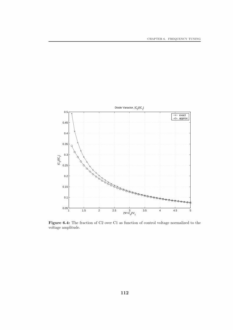
CHAPTER 6. FREQUENCY TUNING
1 1.5 2 2.5 3 3.5 4 4.5 50.05
0.1
0.15
0.2
0.25
0.3
0.35
0.4
0.45
0.5
Diode Varactor, |C2|/|C
1|
(Ψ+V0)/V
1
|C2|/|
C1|
exactapprox
Figure 6.4: The fraction of C2 over C1 as function of control voltage normalized to thevoltage amplitude.
112

6.6. MOS VARACTOR
and
Cmax ≈ CN
√ψ
ψ + V0,max(6.49)
by using the first term of (6.45) only. Inserting (6.47), (6.46), and the firstterm of (6.43), given as
max |C1| ≈ CN
√ψ
ψ + V0,min
(1
2
V1
ψ + V0,min
)(6.50)
in (6.37), we get
max |KAM−PM | ≈ 1
1 − F(I)∆,1H
(I)∆,1
∣∣∣∣∣H
(I)∆,1
H1
∣∣∣∣∣3Qωtune
8ω0
(V1
ψ+V0,min
)2
1 −√
ψ+V0,min
ψ+V0,max
. (6.51)
6.6 MOS Varactor
The MOS structures used when creating transistors in a CMOS process mayalso be used to create capacitors. When used as a tuning capacitor, the MOSstructure is called a varactor. The MOS varactor could either be designed tooperate in inversion or in accumulation [Andreani and Mattisson, 2000].
6.6.1 Background
The large-signal properties of the MOS varactor has recently been investi-gated [Bunch and Raman, 2003, Hegazi and Abidi, 2003], both regardingits impact on tuning characteristics and its impact on the phase noise viaAM-to-PM conversion. In addition to the already known expression for thelarge-signal capacitance, we derive an expression for the maximum AM-to-PM conversion.
6.6.2 Phase Noise Parameters
The small-signal capacitance, c, of an MOS varactor is approximated as
c(v) ≈CL , v ≤ 0CH , v > 0,
(6.52)
where v is the control voltage [Hegazi and Abidi, 2003]. In other words, thecapacitance is equal to CL for negative v and equal to CH for positive v.
113
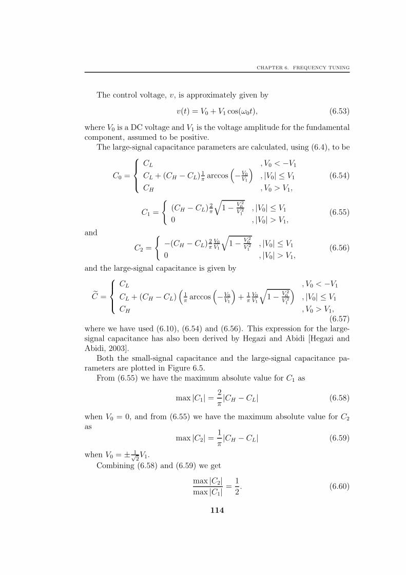
CHAPTER 6. FREQUENCY TUNING
The control voltage, v, is approximately given by
v(t) = V0 + V1 cos(ω0t), (6.53)
where V0 is a DC voltage and V1 is the voltage amplitude for the fundamentalcomponent, assumed to be positive.
The large-signal capacitance parameters are calculated, using (6.4), to be
C0 =
CL , V0 < −V1
CL + (CH − CL)1π
arccos(−V0
V1
), |V0| ≤ V1
CH , V0 > V1,
(6.54)
C1 =
(CH − CL)
2π
√1 − V 2
0
V 21
, |V0| ≤ V1
0 , |V0| > V1,(6.55)
and
C2 =
−(CH − CL)
2πV0
V1
√1 − V 2
0
V 21
, |V0| ≤ V1
0 , |V0| > V1,(6.56)
and the large-signal capacitance is given by
C =
CL , V0 < −V1
CL + (CH − CL)(
1π
arccos(−V0
V1
)+ 1
πV0
V1
√1 − V 2
0
V 21
), |V0| ≤ V1
CH , V0 > V1,(6.57)
where we have used (6.10), (6.54) and (6.56). This expression for the large-signal capacitance has also been derived by Hegazi and Abidi [Hegazi andAbidi, 2003].
Both the small-signal capacitance and the large-signal capacitance pa-rameters are plotted in Figure 6.5.
From (6.55) we have the maximum absolute value for C1 as
max |C1| =2
π|CH − CL| (6.58)
when V0 = 0, and from (6.55) we have the maximum absolute value for C2
as
max |C2| =1
π|CH − CL| (6.59)
when V0 = ± 1√2V1.
Combining (6.58) and (6.59) we get
max |C2|max |C1|
=1
2. (6.60)
114

6.6. MOS VARACTOR
−1 −0.8 −0.6 −0.4 −0.2 0 0.2 0.4 0.6 0.8 1−0.4
−0.2
0
0.2
0.4
0.6
0.8
1MOS Varactor
V0/V
1
c−
CL, C
0−C
L, C1, C
2, C−
CL/
(CH
−C
L)
c(v)C
0C
1C
2C
Figure 6.5: Normalized small-signal and large-signal capacitances as function of thecontrol voltage normalized to the voltage amplitude for the MOS varactor.
115
CHAPTER 6. FREQUENCY TUNING
For the MOS varactor we also have that the maximum tuning range,ωtune, is approximately given as
ωtune ≈∣∣∣∣∂ω0
∂C
∣∣∣∣ |CH − CL| =V1 max |KV CO|
max |C1||CH − CL| =
π
2V1 max |KV CO|,
(6.61)where we have used (6.19). Inserting (6.61), (6.60), and (6.58) in (6.37) gives
max |KAM−PM | ≈ 1
1 − F(I)∆,1H
(I)∆,1
∣∣∣∣∣H
(I)∆,1
H1
∣∣∣∣∣2Qωtuneπω0
. (6.62)
6.7 Summary
We have shown that there are several ways to minimize the AM-to-PM con-version due to the varactor. In addition to having an amplitude-regulatingmechanism that minimizes the AM-to-PM conversion or splitting the tuningrange into several smaller tuning ranges, thereby decreasing the VCO tuningconstant, we may choose a varactor giving low AM-to-PM conversion. Thekey choice is to get a varactor having a low fraction max |C2|
max |C1| , where C1 and
C2 are defined in (6.4).The simple varactors used today, the diode varactor and the MOS var-
actor, have a fraction max |C2|max |C1| in the order of a few tenths. However, several
components may be combined to create varactors having capacitance curvesdifferent than those of the components, thereby reducing the fraction max |C2|
max |C1|compared to the components alone [Levantino et al., 2004]. In these com-pound varactors, the components do not necessarily have one terminal signalgrounded.
116

Chapter 7Phase-Noise Calculations
T hermal and shot noise within the oscillator give a lower bound on theminimum achievable phase noise. This noise arises both in the feed-back network due to lossy components and in the active components,
e.g. transistors. In addition to thermal and shot noise, we also have com-ponents generating 1/f noise. The phase noise originating from 1/f noisemay dominate the phase-noise performance at small frequency offsets fromthe carrier. Apart from these noise sources, we may also have disturbancesoriginating from outside the circuit, such as noise on the supply voltage ornoise coupled capacitively or magnetically into the circuit.
In this chapter I derive expressions for the phase noise of oscillators usingthe method of Impulse Sensitivity Functions (ISFs). The expressions usedfor the ISFs are derived in Chapter 8.
7.1 Introduction
Phase noise has been the topic of extensive research during the last decades.In 1966, a simple formula describing the spectral density of the phase noisewas given by Leeson [Leeson, 1966]; it contained several unknown noise pa-rameters. Later work has been devoted to the calculation of these noiseparameters [Huang, 1998, Hajimiri and Lee, 1998, Samori et al., 1998, Raeland Abidi, 2000, Samori et al., 2000]
On the numerical simulator side, work has been devoted to the implemen-tation of fast and accurate predictions of the phase noise [Kaertner, 1990,Demir, 1998, Kundert, 1999, Demir et al., 2000]. These methods are, how-ever, not suitable to use when deriving closed-form analytical expressions forthe phase noise.
117

CHAPTER 7. PHASE-NOISE CALCULATIONS
Usually, some accuracy in the prediction of a performance measure may besacrificed if we can attain a simple analytical expression for the performancemeasure from which we can obtain design insights. In this chapter we usethe method of Impulse Sensitivity Functions (ISFs) to derive closed-formexpressions for the phase noise [Hajimiri and Lee, 1998, Vanassche et al.,2003].
7.1.1 Assumptions
In Appendix B it is shown that one may calculate the single-sided phase-noise spectral density, L, at a large frequency offset, ωm, from the oscillationfrequency, ω0, as
L[ωm] =Sy(ωm)
2ω2m
, (7.1)
where Sy is the averaged single-sideband noise spectral density. All spectraldensities in this chapter are assumed to be single sided.
We assume that the active part is a transconductance with small delaycompared to the oscillation period, 1/ω0. Consequently, the feedback partmust be a transresistance and is best described by its Z-parameters, definedin Appendix D. We use Zmn as a short form for Zmn(ω0), where ω0 is theoscillation frequency.
7.2 Phase Noise due to White Noise
The thermal noise and shot noise in lossy components are sources of whitenoise. The power spectral density, Sy, for these types of noise is constant withfrequency for all frequencies of interest. Hence, the averaged noise spectraldensity, Sy, is also white with the spectral density given by
Sy = Γ2ySy, (7.2)
where Γy is the Impulse Sensitivity Function (ISF). The over-line is used todenote time averaging. The two main ISFs we use in this chapter are Γx forvoltage noise entering at the input to the active part and Γy for current noiseentering at the output of the active part.
7.2.1 Noise from Feedback Network
We assume that the feedback network is fairly linear such that the equivalentthermal noise spectral density at the output of the passive feedback network,
118

7.2. PHASE NOISE DUE TO WHITE NOISE
h, can be calculated as
Sx,h(ω, t) = 4kBTℜ[Z22(ω)], (7.3)
where kB is the Boltzmann constant, T is the temperature and Z22 is theoutput impedance of the feedback network, h, [Pettai, 1984, Bennett, 1960].The noise spectral density of passive two-port networks is further discussedin Appendix D.
For oscillators with a feedback network with a fairly high Q-value wecan assume that the noise is non-negligible only around the fundamentalfrequency, ω0, and we consequently have to consider just the fundamentalcomponent of the ISF.
Since the noise spectral density is constant with time the averaged noisespectral density is simply
Sx,h(ωm) ≈ 1
2|Γx,1|2Sx,h(ω0) = 2kBTℜ[Z22]|Γx,1|2. (7.4)
We can rewrite the ISF using
ℑ[Γx,1] =ℑ[Γy,1]
H1
=ℑ[Γy,1]
Z21
(7.5)
and
ℜ[Γx,1] =ℜ[Γy,1]
H(I)∆,1
=ℜ[Γy,1]
Z(I)∆,21
, (7.6)
using (8.68) and (8.69) from Chapter 8, where H1 and Z21 are the large-
signal transfer functions for the feedback part and H(I)∆,1 and Z
(I)∆,21 are the
incremental large-signal transfer functions for the feedback part.If the feedback network is almost linear, we can approximate Z
(I)∆,21 with
Z21 and we get
Γx,1 ≈Γy,1Z21
. (7.7)
We can now write the average noise spectral density as
Sx,h(ωm) ≈ 2kBTℜ[Z22]|Γy,1|2Z2
21
. (7.8)
If possible, we should choose feedback networks that fulfill
ℜ[Z11]ℜ[Z22] ≈ Z221 (7.9)
119

CHAPTER 7. PHASE-NOISE CALCULATIONS
in order to minimize the phase noise due to noise from the feedback network.We then get the average noise spectral density as
Sx,h(ωm) ≈ 2kBT
ℜ[Z11]|Γy,1|2; (7.10)
see also Appendix D.3.The average noise spectral density given in (7.10) can be rewritten as
Sx,h(ωm) ≈ 2kBTℑ[Γy,1]2
ℜ[Z11]
(1 +
ℜ[Γy,1]2
ℑ[Γy,1]2
), (7.11)
where we have expanded the absolute value of the fundamental componentof the ISF, Γy,1, in a real and an imaginary part.
7.2.2 Noise from Active Network
We assume that the output noise spectral density of the active part, f , isproportional to the incremental gain of the active part according to
Sy,g(ω, t) = 4kBTγ|g′(X1 cos(ω0t))|, (7.12)
where γ is a proportionality constant equal to 1/2 for bipolar circuits and2/3 for circuits with FETs, but may be higher for MOSFETs with highelectrical fields. This assumption is true both for one-transistor stages andfor differential stages as shown in Appendix C.
Since the transconductance is a periodic function with angular frequencyω0 we can write it as a Fourier series according to
|g′(X1 cos(ω0t))| =
∞∑
n=0
G′n cos(nω0t). (7.13)
We can now calculate the averaged noise spectral density, assuming that thefundamental component of the ISF is dominant, to be
Sy,g(ωm) ≈ 4kBTγ
(1
2G′
0Γy,1Γ∗y,1 +
1
8G′
2
(Γ2y,1 + Γ∗
y,12))
, (7.14)
which can be rewritten using the real and imaginary parts of Γy,1 as
Sy,g(ωm) ≈ 4kBTγ
(1
2G′
0
(ℜ[Γy,1]
2 + ℑ[Γy,1]2)
+1
4G′
2
(ℜ[Γy,1]
2 − ℑ[Γy,1]2))
.
(7.15)
120

7.2. PHASE NOISE DUE TO WHITE NOISE
This expression can be rewritten as
Sy,g(ωm) ≈ 2kBTγ(|G(I)
∆,1|ℜ[Γy,1]2 + |G1|ℑ[Γy,1]
2)
(7.16)
using results from Appendix A.2, where G(I)∆,1 is the incremental large-signal
transconductance and G1 is the large-signal transconductance of the activepart, excluding any amplitude-regulating loop.
This expression can be rewritten once more as
Sy,g(ωm) ≈ 2kBTℑ[Γy,1]2
ℜ[Z11]γ
(ℜ[Z11]
|Z21|+ ℜ[Z11]|G(I)
∆,1|ℜ[Γy,1]
2
ℑ[Γy,1]2
), (7.17)
using that
G1 = F1 =1
H1
=1
Z21, (7.18)
where we have used the Barkhausen criterion, F1H1 = 1, where F1 and H1 arethe large-signal gains of the active and feedback parts, respectively. Observethat G
(I)∆,1 is not equal to F
(I)∆,1 when an explicit amplitude control is used.
In addition to the noise from transistors already treated in this sectionwe also have shot noise from the base–emitter junction in the bipolar tran-sistor, induced gate noise in the field-effect transistor, and noisy base or gateresistances.
As shown in Appendix C, base shot noise may be neglected since thetransistor is voltage-driven and induced gate noise may be neglected whenthe operation frequency is substantially lower than the transit frequency forthe transistors.
7.2.3 Noise from Series Base and Gate Resistances
Noise from series base and gate resistances does not get filtered by the feed-back network since these noise sources are located directly at the input tothe active part. Consequently, we must use the total ISF for the input to theactive part, Γx, and cannot neglect any of its harmonics.
Neglecting the AM-to-PM conversion of noise, we can use the ISF givenin (8.26) as its frequency components, repeated here for convenience:
Γx,n = jnFnω0
|X1|F1Q=nFn
F1
Γx,1. (7.19)
The voltage noise from the series base or gate resistance, RI , is given by
Sx,i = 4kBTRI . (7.20)
121

CHAPTER 7. PHASE-NOISE CALCULATIONS
The averaged noise spectral density is given by
Sx,i = Sx,i
(|Γx,0|2 +
1
2
∞∑
n=1
|Γx,n|2)
= Sx,i|Γx,1|2
2
∞∑
n=1
|Γx,n|2|Γx,1|2
. (7.21)
Combining (7.19), (7.20) and (7.21), we get the averaged noise spectral den-sity as
Sx,i = 2kBT |Γx,1|2∞∑
n=1
n2|Fn|2
|F1|2. (7.22)
Using (8.69), we may rewrite this expression as
Sx,i =2kBTℑ[Γy,1]
2
ℜ[Z11]
RI
ℜ[Z11]
ℜ[Z11]2
Z221
∞∑
n=1
n2|Fn|2
|F1|2. (7.23)
We see that the amount of harmonics in the oscillator, coming from the non-linearity in the transistor, affects the amount of phase noise due to series baseand gate resistances. Since the nonlinearity of the transistor increases withinput amplitude to the transistor, the phase noise increases with increasinginput amplitude.
7.2.4 Noise from Diode Limiting
We next calculate the contribution from the diodes to the phase noise. Inthis section, we assume the diode series resistance to be negligible. FromAppendix C we have that the noise current spectral density from a diode isgiven by
Sd(ω, t) = 2kBTgac(vAC(t)) = 2kBTgac(Vac,0 + Vac,1 cos(ω0t)), (7.24)
where Vac,0 and Vac,1 are the DC voltage and fundamental voltage amplitudeacross the diode, respectively, vAC is the total voltage across the diode, andthe small-signal conductance of the diode, gac, is given by
gac =∂iD∂vAC
=iDVT, (7.25)
where iD is the diode current and VT is the thermal voltage.Since the conductance is a periodic function with angular frequency ω0,
we can express it as a Fourier series according to
gac(Vac,0 + Vac,1 cos(ω0t)) =∞∑
n=0
I ′dn cos(nω0t). (7.26)
122

7.2. PHASE NOISE DUE TO WHITE NOISE
We can now calculate the averaged noise spectral density, assuming that thefundamental component of the ISF is dominant, to be
Sd(ωm) ≈ 2kBT
(1
2I ′d0Γd,1Γ
∗d,1 +
1
8I ′d2
(Γ2d,1 + Γ∗
d,12))
, (7.27)
where Γd,1 is the ISF for noise currents parallel to the diode. This expressioncan be rewritten using the real and imaginary parts of Γd,1 as
Sd(ωm) ≈ 2kBT
(1
2I ′d0
(ℜ[Γd,1]
2 + ℑ[Γd,1]2)
+1
4I ′d2
(ℜ[Γd,1]
2 − ℑ[Γd,1]2))
.
(7.28)This expression can be rewritten once more as
Sd(ωm) ≈ kBT(Gac
(I)
∆,1ℜ[Γd,1]2 + Gac1ℑ[Γd,1]
2), (7.29)
using results from Appendix A.2. From Appendix C.1, we have that
Gac1 =Id,1Vac,1
(7.30)
and
Gac
(I)
∆,1 ≈Id,1VT
= Gac1
Vac,1VT
. (7.31)
In most cases ℜ[Γd,1] is inversely proportional to Gac
(I)
∆,1 and we can ap-proximate the averaged noise spectral density with
Sd(ωm) ≈ kBTGac1ℑ[Γd,1]2 (7.32)
when Vac,1 ≫ VT , which is half the noise we would expect from a resistor
with conductance Gac1 inserted instead of the diode.
7.2.5 Noise from Biasing Network
Apart from the noise inherent to the oscillator core, we also have noise origi-nating in the biasing network. The bias network is not part of the oscillatorhigh-frequency feedback loop, but is nevertheless necessary for the activepart to function properly. It sets the operating point such that the oscillatorstarts and regulates the oscillation amplitude once it has started.
We consider two types of biasing networks in detail: biasing using tran-sistors and biasing using resistors. Preferably, the Q-value of the oscillatoris not affected by the biasing components. If the Q-value is affected, theQ-value including the bias network should be used during calculations wherethe Q-value is needed.
123

CHAPTER 7. PHASE-NOISE CALCULATIONS
Unfiltered Bias Current for Differential Pairs
We assume the phase shift of the active part, ζ , to be unaffected by thenoise from the current bias. If this assumption is not fulfilled, we need thecomplete ISF for the current bias noise source including the sensitivity for ζwith respect to the bias current.
The phase noise due to noise in the current bias for differential stagescould be calculated either using the ISF of Section 8.5 or by transformingthe noise source to a corresponding noise source at the output of the activepart. Here we choose to use the latter method.
The spectral density of the equivalent noise source located at the outputof the active part, f , as a function of time, t, is given by
Sy,b(t) = Ai(t)2Sb (7.33)
where Ai is the instantaneous small-signal current gain from the bias currentto the output of the active part, given for differential pairs based on bipolartransistors and field-effect transistors in Appendix C. The noise spectraldensity for the bias current source is denoted Sb.
The averaged noise spectral density is
Sy,b = Γy(ω0t)2Ai(t)2Sb, (7.34)
where the over-line is used to denote time averaging. Assuming that thefundamental component for the ISF for noise entering at the output of theactive part is dominant, we get the averaged noise spectral density as
Sy,b ≈(ℜ[Γy,1]
2
(A0
2+A2
4
)+ ℑ[Γy,1]
2
(A0
2− A2
4
))Sb, (7.35)
where we write the squared small-signal current gain as a Fourier series ac-cording to
Ai(t)2 =
∞∑
n=0
An cos(nω0t). (7.36)
The two factors
Kre =A0
2+A2
4(7.37)
and
Kim =A0
2− A2
4(7.38)
are plotted as function of the input amplitude to the active block, both forFET and BJT differential pairs, in Appendix C. Each of the two factors Kre
124

7.2. PHASE NOISE DUE TO WHITE NOISE
and Kim has an upper limit of 1/8. Hence, an upper limit of the averagedspectral density is given by
Sy,b ≈(Kreℜ[Γy,1]
2 +Kimℑ[Γy,1]2)Sb ≤
Sb8|Γy,1|2, (7.39)
where the equality is reached as the input amplitude goes to infinity, i.e.instantaneous switching of the differential pair. In this extreme case half thebias noise ends up as differential noise at the output of the active part; theother half ends up as common-mode noise.
The noise spectral density, Sb, for a current-source transistor is given by
Sb = 4kBTγgm,b, (7.40)
where gm,b is the transconductance for the current-source transistor. Thenoise spectral density for a current-determining resistor, RB, is given by
Sb = 4kBT1
RB
. (7.41)
The averaged noise spectral density for a transistor-based current sourceis
Sy,b(ωm) = 4kBTγgm,b(Kreℜ[Γy,1]
2 +Kimℑ[Γy,1]2)
(7.42)
and for a resistor-based current source it is
Sy,b(ωm) =4kBT
RB
(Kreℜ[Γy,1]
2 +Kimℑ[Γy,1]2). (7.43)
Rewriting the expression for the averaged noise spectral density of atransistor-based current source, we get
Sy,b(ωm) =2kBTℑ[Γy,1]
2
ℜ[Z11]2γgm,bℜ[Z11]
(Kre +Kim
ℜ[Γy,1]2
ℑ[Γy,1]2
), (7.44)
and for a resistor-based current source, we get
Sy,b(ωm) =2kBTℑ[Γy,1]
2
ℜ[Z11]
2ℜ[Z11]
RB
(Kre +Kim
ℜ[Γy,1]2
ℑ[Γy,1]2
). (7.45)
In a technology using bipolar transistors, a current-source transistor hasa transconductance of gm,b = 4Gm since it conducts twice as much currentas one of the transistors in the differential pair when in equilibrium andthe small-signal transconductance for the differential stage, Gm, is half thetransconductance of one of the transistors in the differential pair in equilib-rium.
125

CHAPTER 7. PHASE-NOISE CALCULATIONS
Unfiltered Bias Current at Output
A white noise source situated at the input to the feedback network can betreated in the same way as the noise from the active part. The averagedspectral density is given by
Sy,b ≈1
2|Γy,1|2Sy,b, (7.46)
where Sy,b is the noise spectral density for the bias.A transistor used as bias current source will have an averaged noise spec-
tral density of
Sy,b(ωm) =2kBTℑ[Γy,1]
2
ℜ[Z11]γgm,bℜ[Z11]
(1 +
ℜ[Γy,1]2
ℑ[Γy,1]2
), (7.47)
where gm,b is the transconductance of the bias transistor. A bias resistor,RB, gives an averaged noise spectral density of
Sy,b(ωm) =2kBTℑ[Γy,1]
2
ℜ[Z11]
ℜ[Z11]
RB
(1 +
ℜ[Γy,1]2
ℑ[Γy,1]2
). (7.48)
Unfiltered Bias Current at Input
The averaged noise spectral density for a voltage noise source at the inputto the active block is given by
Sx,b ≈1
2|Γx,1|2Sx,b (7.49)
where Γx is the ISF for noise entering at the input to the active block andSx is the noise spectral density. We can rewrite the ISF using
ℑ[Γx,1] =ℑ[Γy,1]
H1
=ℑ[Γy,1]
Z21(7.50)
and
ℜ[Γx,1] =ℜ[Γy,1]
H(I)∆,1
=ℜ[Γy,1]
Z(I)∆,21
(7.51)
using (8.68) and (8.69) and where Z(I)∆,21 = H
(I)∆,1.
We assume that the output impedance for signals in quadrature phasewith the input to the active block is equal to Z22, and that the outputimpedance for signals in phase with the input to the active block is equalto Z
(I)∆,22. Using these two output impedances and assuming that the input
126

7.2. PHASE NOISE DUE TO WHITE NOISE
current noise is white, we rewrite the noise current source with spectral den-sity Sb into two noise voltage sources at the input to the active part: one inquadrature phase with the oscillator with noise voltage spectral density
S(Q)x,b = |Z22|2Sb, (7.52)
and one in phase with the oscillator with noise voltage spectral density
S(I)x,b = |Z(I)
∆,22|2Sb. (7.53)
The averaged spectral density can be written as
Sx,b =1
2
(ℑ[Γx,1]
2S(Q)x,b + ℜ[Γx,1]
2S(I)x,b
), (7.54)
which can be expressed as
Sx,b =1
2
(|Z22|2ℑ[Γx,1]
2 + |Z(I)∆,22|2ℜ[Γx,1]
2)Sb, (7.55)
using (7.52) and (7.53). Rewriting this expression in terms of Γy,1, we get
Sx,b ≈1
2
|Z22|2Z2
21
ℑ[Γy,1]2 +
|Z(I)∆,22|2(
Z(I)∆,21
)2ℜ[Γy,1]2
Sb, (7.56)
using (7.50) and (7.51). Assuming that
|Z22|Z21
≈|Z(I)
∆,22|Z
(I)∆,21
, (7.57)
a final rewriting gives
Sx,b ≈2kBTℑ[Γy,1]
2
ℜ[Z11]γgm,bℜ[Z11]
|Z22|2Z2
21
(1 +
ℜ[Γy,1]2
ℑ[Γy,1]2
)(7.58)
when the current source is a transistor with transconductance gm,b and
Sx,b ≈2kBTℑ[Γy,1]
2
ℜ[Z11]
ℜ[Z11]
RB
|Z22|2Z2
21
(1 +
ℜ[Γy,1]2
ℑ[Γy,1]2
)(7.59)
when the bias current source is a resistor RB.
127

CHAPTER 7. PHASE-NOISE CALCULATIONS
Filtered Bias Current
Since the bias current is low-pass filtered, it does no longer possess a whitespectrum. The averaged noise spectrum for a noise source having a low-passspectrum is given in Section 7.3.3 which treats bias sources having 1/f noise.The averaged noise spectral density is given by (7.89) as
Sw,b(ωm) =|Y1|2
4
(ℜ[Γy,1]
1
B
∂B
∂W0
+ ℑ[Γy,1]∂ζ
∂W0
)2
Sw,b(ωm), (7.60)
where Sw,b is the noise spectral density for the bias current source.A transistor used as bias current source has an averaged noise spectral
density of
Sy,b(ωm) =2kBTℑ[Γy,1]
2
ℜ[Z11]
γgm,bℜ[Z11]
2
(∂ζ
∂W0|Y1| +
ℜ[Γy,1]
ℑ[Γy,1]
∂B
∂W0|X1|
)2
,
(7.61)where gm,b is the transconductance of the bias transistor. A bias resistor,RB, gives an averaged noise spectral density of
Sy,b(ωm) =2kBTℑ[Γy,1]
2
ℜ[Z11]
ℜ[Z11]
2RB
(∂ζ
∂W0|Y1| +
ℜ[Γy,1]
ℑ[Γy,1]
∂B
∂W0|X1|
)2
. (7.62)
Under the assumption that ∂ζ∂W0
≈ 0 we get
Sy,b(ωm) =2kBTℑ[Γy,1]
2
ℜ[Z11]
γgm,bℜ[Z11]
2
ℜ[Γy,1]2
ℑ[Γy,1]2
(∂B
∂W0
)2
|X1|2 (7.63)
when a transistor is used as bias source, and
Sy,b(ωm) =2kBTℑ[Γy,1]
2
ℜ[Z11]
ℜ[Z11]
2RB
ℜ[Γy,1]2
ℑ[Γy,1]2
(∂B
∂W0
)2
|X1|2 (7.64)
when a resistor is used as bias source. In both cases we have that
∂B
∂W0|X1| ≤
2
π(7.65)
for a differential pair, where the equality is reached when the transistors inthe differential pair are switching instantaneously, and
∂B
∂W0|X1| ≤ 2 (7.66)
for a single transistor, where the equality is reached when the transistor isoperating in deep Class C.
128

7.2. PHASE NOISE DUE TO WHITE NOISE
7.2.6 Total Noise
Summing up the contributions of all white noise sources, we write the totalaveraged noise spectral density as
Sy,tot(ωm) ≈ 2kBTFℑ[Γy,1]2
ℜ[Z11], (7.67)
where
F ≈ 1+ℜ[Γy,1]
2
ℑ[Γy,1]2+ γ
ℜ[Z11]
|Z21|+ γ
ℜ[Γy,1]2
ℑ[Γy,1]2|G(I)
∆,1|ℜ[Z11] +K1K2 +K1K3ℜ[Γy,1]
2
ℑ[Γy,1]2
(7.68)is the noise factor.
This noise factor can be rewritten as
F ≈ 1 + γℜ[Z11]
|Z21|+K1K2 +K2
AM−PM
(1 + γ|G(I)
∆,1|ℜ[Z11] +K1K3
), (7.69)
where KAM−PM is the AM-to-PM conversion factor defined as
KAM−PM =ℜ[Γy,1]
ℑ[Γy,1]. (7.70)
The constant K1 depends on the bias current noise source and is givenby
K1 = γgm,bℜ[Z11] (7.71)
for a bias transistor with transconductance gm,b and
K1 =ℜ[Z11]
RB(7.72)
for a bias resistor RB.The constants K2 and K3 depend on where the bias current is located
and are given by
K2 =
2Kim ≤ 14
differential pair tail bias1 bias at output|Z22|2Z2
21bias at input
(7.73)
and
K3 =
2Kre ≤ 14
differential pair tail bias1 bias at output|Z22|2Z2
21bias at input
(7.74)
129

CHAPTER 7. PHASE-NOISE CALCULATIONS
From (8.66) in Chapter 8 we have that
ℑ[Γy,1] ≈ω0
|Y1|Q(7.75)
and from (7.1) we get the phase noise as
L[ωm] ≈ Sy(ωm)
2ω2m
≈ kBTF
2P1Q2
ω20
ω2m
, (7.76)
where we have used (7.75), (7.67) and where
P1 =ℜ[Z11]|Y1|2
2(7.77)
is the fundamental power delivered to the feedback network, h. This ex-pression for the single-sided phase noise is equal to the one given by Leeson[Leeson, 1966], with the noise factor given by (7.69).
A theoretical lower limit for the noise factor is given by
F ≥ 1 + γ (7.78)
for active blocks where the input-voltage amplitude to the active block doesnot exceed the output-voltage amplitude of the active block. If higher input-voltage amplitude is allowed, the theoretical lower limit for the noise factor,F , is unity, where the phase noise is limited by the noise from the feedbacknetwork, h, alone.
7.3 Phase Noise due to 1/f Noise
The 1/f noise originates from imperfections in the components and dependson the technology. The spectral density for these noise sources is approxi-mately inversely proportional to the frequency.
The averaged noise spectral density due to 1/f noise is given by
Sy(ωm) =
(Γy(ω0t)
√Sy(ωm, t)
)2
(7.79)
where Sy(ωm, t) is the noise spectral density at offset angular frequency ωmat time instant t [Hajimiri and Lee, 1998]. However, this expression is notvalid at very small frequency offsets [Klimovitch, 2000], but we are seldominterested in the phase noise at such small frequency offsets.
In the special case when Sy is constant with time, (7.79) simplifies to
Sy(ωm) = Γ2y,0Sy(ωm). (7.80)
130

7.3. PHASE NOISE DUE TO 1/F NOISE
7.3.1 Noise from Feedback Network
We assume that the feedback network has negligible 1/f noise compared tothe active devices. Noise entering at the tuning port is not dealt with in thischapter since it does not originate from the oscillator core.
7.3.2 Noise from Active Network
The transistors in the active network contribute a considerable amount of1/f noise, which is converted into phase noise through several mechanisms.In addition to modulating the active part itself, as treated below, it maycontribute by direct low-frequency modulation of varactors which gives ad-ditional phase noise.
We now consider the case where the 1/f noise modulates the active part.We assume that the emitter/source terminal sees a high impedance at lowfrequencies, i.e. the transistor or differential pair is biased by a currentat this node. We also assume that the other nodes, i.e. base/gate andcollector/drain terminals, are at low impedance at low frequencies, whichmeans they have fixed low-frequency voltage potentials. We also assumethat noise components at frequencies higher than the oscillation frequencyare filtered out by the feedback network.
We now move the 1/f noise sources from between base–emitter and drain–source, as described in Appendix C, to be parallel with the bias current. Thenoise spectral density for the low-frequency components in the BJT case isgiven by
Sw,f(ωm) ≈ 2πK1/f
ωm
IDCβ, (7.81)
using (C.18), where IDC is the bias current which is approximately equal tothe collector current if the current amplification factor, β, is large. We arriveat this expression both for single transistors by considering the DC value ofthe current only and for differential pairs where we add the two contributionsto get a constant noise spectral density with time. The noise spectral densityfor the low-frequency components in the FET case is given by
Sw,f(ωm) ≈ 2πK1/f
ωmIDC , (7.82)
using (C.32), where IDC is the bias current.Considering the low-frequency components only, the averaged noise spec-
tral density is given by
Sw,f(ωm) ≈ Γ2w,0Sw,f(ωm), (7.83)
131

CHAPTER 7. PHASE-NOISE CALCULATIONS
where Sw,f is the noise spectral density given above, and Γw,0 is the DCcomponent of the ISF for the current source given by
Γw,0 =|Y1|2
(ℜ[Γy,1]
1
B
∂B
∂W0+ ℑ[Γy,1]
∂ζ
∂W0
)(7.84)
according to (8.87) in Chapter 8. Combining these two expressions, we getthe averaged noise spectral density as
Sw,f(ωm) =|Y1|2
4
(ℜ[Γy,1]
1
B
∂B
∂W0+ ℑ[Γy,1]
∂ζ
∂W0
)2
Sw,f(ωm). (7.85)
Finally, by inserting (7.81) or (7.82) in (7.85) we get
Sw,f(ωm) =|Y1|2
4
(ℜ[Γy,1]
1
B
∂B
∂W0+ ℑ[Γy,1]
∂ζ
∂W0
)2 2πK1/f,fIDCωm
, (7.86)
where K1/f,f =K1/f
βfor a BJT implementation and K1/f,f = K1/f for an
FET implementation.
7.3.3 Noise from Biasing Network
In this section we treat low-frequency noise coming from the biasing network.The noise is assumed to have a spectral density, Sb, which is constant withtime.
The averaged noise spectral density is given by
Sw,b(ωm) = Γ2w,0Sb(ωm), (7.87)
where Sb is the noise spectral density of the bias network controlling the biascurrent of the active network, and Γw,0 is the DC component of the ISF forthe current source given by
Γw,0 =|Y1|2
(ℜ[Γy,1]
1
B
∂B
∂W0
+ ℑ[Γy,1]∂ζ
∂W0
)(7.88)
according to (8.87) in Chapter 8. Combining these two expressions, we getthe averaged noise spectral density as
Sw,b(ωm) =|Y1|2
4
(ℜ[Γy,1]
1
B
∂B
∂W0+ ℑ[Γy,1]
∂ζ
∂W0
)2
Sb(ωm). (7.89)
132

7.3. PHASE NOISE DUE TO 1/F NOISE
Assuming that the noise spectral density of the bias network is propor-tional to the DC current, IDC , supplied to the active part, we may write thenoise spectral density as
Sb(ωm) =2πK1/f,bIDC
ωm, (7.90)
where K1/f,b is a noise constant for the biasing network. The averaged noisespectral density may now be written as
Sw,b(ωm) =|Y1|2
4
(ℜ[Γy,1]
1
B
∂B
∂W0+ ℑ[Γy,1]
∂ζ
∂W0
)2 2πK1/f,bIDCωm
. (7.91)
The noise from the bias current network also contributes to the phasenoise by another mechanism, via direct modulation of any nonlinear reactivecomponents. This term may be added to the ISF for the bias current, Γw,0,if deemed significant.
Modulated Noise from Biasing Network
In some special cases of amplitude regulating circuits, the current noise sourceis voltage starved during a fraction of the oscillation period in order to de-crease the average current. An example is the tail bias current for a dif-ferential stage where the common emitter/source node tracks the voltagewaveform at the collector/drain nodes and may get lower than the voltageheadroom needed for the current source to act as a current source. Conse-quently, the average current decreases, limiting the voltage amplitude. Thismodulation of the current source also modulates its noise sources, changingtheir frequency properties.
7.3.4 Total Noise
We sum the 1/f noise contribution from the active part, given in (7.86), withthe contribution from the bias network, given by (7.91), to get the totalaveraged noise spectral density as
Sw(ωm) =|Y1|2
4
(ℜ[Γy,1]
1
B
∂B
∂W0+ ℑ[Γy,1]
∂ζ
∂W0
)2 2π(K1/f,f +K1/f,b)
ωmIDC .
(7.92)Inserting this expression in the expression for the phase noise, given by
L[ωm] =Sw(ωm)
2ω2m
, (7.93)
133
CHAPTER 7. PHASE-NOISE CALCULATIONS
we get the phase noise due to 1/f noise as
L[ωm] =2π(K1/f,f +K1/f,b)IDC |Y1|2ℑ[Γy,1]
2
8ω3m
(ℜ[Γy,1]
ℑ[Γy,1]
1
B
∂B
∂W0+
∂ζ
∂W0
)2
.
(7.94)We see that the 1/f noise has been upconverted to phase noise with a spectraldensity proportional to 1/f 3. We can rewrite this expression using (7.70) and(7.75) as
L[ωm] =2π(K1/f,f +K1/f,b)IDC
8Q2
(KAM−PM
1
B
∂B
∂W0+
∂ζ
∂W0
)2ω2
0
ω3m
. (7.95)
Sometimes it is of interest to know the corner frequency, ωm,1/f , betweenthe phase noise obeying the 1/f 2 spectrum and that obeying the 1/f 3 spec-trum. By equating (7.76) and (7.95), we get the corner frequency as
ωm,1/f =2π(K1/f,f +K1/f,b)IDCP1
4kBTF
(KAM−PM
1
B
∂B
∂W0+
∂ζ
∂W0
)2
. (7.96)
We see that in order to minimize phase noise due to 1/f noise we mustchoose components with low 1/f noise, minimize the AM-to-PM conversion,and minimize the phase sensitivity to bias current variations in the activepart.
7.4 Phase Noise due to Disturbances
In addition to the noise sources treated so far, we have disturbances from thephysical surrounding of the oscillator. These disturbances are usually deter-ministic, but may in some cases be treated as random in nature dependingon the properties of the disturbances.
Examples of disturbances are noise on supply and ground lines, electricand magnetic fields coupling into the oscillator, and noise in the substrate ofintegrated circuits.
Depending on the properties of the disturbances, different ways to calcu-late the resulting spectra are appropriate. If the disturbance can be treatedas a stochastic process with a given spectra, the methods used to calculatephase noise due to white noise or 1/f noise explained earlier in this chaptercan be used. If the disturbance is a periodic signal, for example a sinusoid,the analysis of Section 7.5 can be used.
134

7.5. INJECTION LOCKING
7.5 Injection Locking
If the frequency of a disturbance is close enough to one of the harmonicsof the oscillator and the signal level of the disturbance is high enough, theoscillator may lock to the disturbing signal. We here calculate the injectedlevel needed at a given frequency offset for an injection lock to occur. Weassume that the injected signal strength is still low enough for the change inoscillation frequency to be linear with respect to the injected signal strength.
The input signal is a sinusoid according to
e(t) = En cos(n(ω0 + ω∆)t), (7.97)
where En is the input amplitude, ω0 is the free-running frequency of theoscillator, and ω∆ is the change in oscillation frequency when the oscillatorhas locked to the input signal.
We start with the differential equation describing the average input phaseas a function of time given by
dθ
dt= Γe(ω0t+ θ)e(t), (7.98)
where θ is the averaged phase, Γe is the Impulse Sensitivity Function (ISF)for the input signal e, and the over-line is used to denote time averaging.When the oscillator is in lock, we have
θ(t) = ω∆t+ ϕ, (7.99)
where ϕ is the phase difference between the oscillator signal and the inputsignal. Taking the derivative of this expression with respect to time, we get
dθ
dt= ω∆. (7.100)
Inserting this expression in (7.98) and carrying out the averaging, we get thechange in oscillation frequency as
ω∆ =Enℜ[Γne
jnϕ]
2. (7.101)
Given the input amplitude, we see that the change in oscillation frequencymust obey
|ω∆| <En|Γn|
2(7.102)
135

CHAPTER 7. PHASE-NOISE CALCULATIONS
in order for the oscillator to lock to the input signal. Given the change inoscillation frequency, the input amplitude must obey
En >2|ω∆||Γn|
(7.103)
in order for the oscillator to lock to the input signal.If the input signal is not strong enough to make the oscillator lock, we
need to solve the differential equation (7.98), which can be rewritten as
dθ
dt=Enℜ[Γne
jn(θ−ω∆t)]
2(7.104)
for the input signal given in (7.97). If the oscillator does lock, this equationreduces to (7.101) when we use that the averaged phase is now described by(7.99).
7.5.1 Oscillator with Linear Feedback Network
As an example of an injection-locked oscillator, we assume that the feedbacknetwork is linear and that the input signal is injected at the input of theactive block. For these assumptions, we have the frequency components ofthe ISF from (8.26) as
Γe,n = jnFnω0
X1F1Q, (7.105)
where X1 is the fundamental amplitude at the input to the active part, Qis the Q-value of the oscillator and Fn are the describing functions for theactive part, as defined in Appendix A. Concentrating on signals injected atfrequencies close to the fundamental free-running oscillator, we only considerthe fundamental component of the ISF, given as
Γe,1 = jω0
X1Q. (7.106)
Inserting this expression in (7.101), we get the change in oscillation fre-quency as
ω∆ =E1ℜ[Γ1e
jϕ]
2= −E1ω0 sin(ϕ)
2X1Q. (7.107)
Rewriting this expression, we get the expression for the phase differencebetween the injected signal and the oscillator signal as
sin(ϕ) = 2QX1
E1
ω∆
ω0
. (7.108)
136

7.6. SUMMARY
Since the left-hand side must have an absolute value less than unity, theinput amplitude E1 must fulfill
E1
X1> 2Q
|ω∆|ω0
. (7.109)
These two last expressions agree with those given by Adler [Adler, 1946].There is, however, a sign inversion due to the difference in definition of fre-quency offset.
When the oscillator does not lock to the injected signal, we have to cal-culate the averaged phase by inserting (7.106) in (7.104), and the differentialequation to solve is now given by
dθ
dt=E1ℜ[Γ1e
j(θ−ω∆t)]
2= −E1ω0 sin(θ − ω∆t)
2X1Q. (7.110)
This nonlinear differential equation describing the phase evolution with timehas been solved by Stover [Stover, 1966]. For an injected signal, e(t), which ismuch smaller than the oscillator signal, x(t), we get two dominant sidebandsat frequency offset |ω∆| from the free-running frequency ω0, with amplitudesE1
4Qω0
|ω∆| .
7.6 Summary
The phase-noise spectrum of an oscillator due to white noise was derived andthe resulting expression as function of offset frequency, ωm, is given by (7.76)as
L[ωm] ≈ Sy(ωm)
2ω2m
≈ kBTF
2P1Q2
ω20
ω2m
, (7.111)
where kB is the Boltzmann constant, T is the absolute temperature, P1 isthe fundamental power dissipated in the feedback network, Q is Q-value ofthe oscillator, ω0 is the oscillation frequency, and the noise factor, F , is givenby (7.69).
From the expression for the noise factor, we can conclude that the phasenoise is not strongly dependent on the operation of the transistors. As longas the AM-to-PM conversion, KAM−PM , is much less than unity, the noisefactor mainly depends on the voltage gain of the feedback network, the noisefactor γ for the transistors, and the bias network.
We have also derived an expression for the corner frequency, ωm,1/f , be-tween the 1/ω2
m region and the 1/ω3m region, given in (7.96). We conclude
that to minimize phase noise due to 1/f noise, we must choose components
137

CHAPTER 7. PHASE-NOISE CALCULATIONS
with low 1/f noise, minimize the AM-to-PM conversion, and minimize thephase sensitivity to bias current variations in the active part.
Finally, the effect of injection locking due to disturbances has been eval-uated. An expression for the minimum injected amplitude needed to achievea lock as function of the offset frequency was derived using the method ofImpulse Sensitivity Functions (ISFs).
138

Chapter 8Impulse Sensitivity Functions
I n this chapter, I show how one can obtain approximate expressions for theImpulse Sensitivity Functions (ISFs) of oscillators using a new methodbased on Describing Functions (DFs). I also derive the ISFs needed
to calculate the phase noise and sensitivity to disturbances for a generaloscillator modeled as a feedback system.
8.1 Introduction
The Impulse Sensitivity Function (ISF) was proposed by Hajimiri and Lee[Hajimiri and Lee, 1998] as a means for calculating the oscillator phase noise.A way to calculate the ISFs numerically in simulators was then also proposed,where a noise impulse is injected and the resulting phase shift is measuredin a transient analysis. Numerical simulation cannot, however, provide theinsight a closed-form analytical expression does.
Exact analytical calculation of the ISF has been performed for simplesystems [Falk and Schwarz, 2000, Falk and Schwarz, 2003, Zhang et al., 2004],but the calculation is often too cumbersome and often restricted to specifictopologies, such as those which can be described as second-order systems.An approximative way to calculate the ISFs for an oscillator based on thederivatives of the signal waveform has also been proposed [Hajimiri and Lee,1998]. This method is, however, limited to the case where no AM-to-PMconversion of noise occurs within the oscillator.
In this chapter, we introduce a method for calculating the ISF whichyields simple expressions at the expense of some accuracy. The method isbased on the describing-function method [Atherton, 1975, Gelb and Velde,1968]. The method gives valid results when the feedback network in the
139

CHAPTER 8. IMPULSE SENSITIVITY FUNCTIONS
oscillator is of bandpass character, that is, in oscillators with a relativelyhigh Q-value. Errors related to this assumption are discussed in Chapter 9where calculations are compared to simulations. A short introduction toDescribing Functions (DFs) and Incremental Describing Functions (IDFs) isgiven in Appendix A.
8.1.1 Definition of Impulse Sensitivity Function
Before continuing with the derivation of Impulse Sensitivity Functions (ISFs),we first need to define the ISF. The differential equation describing the phaseevolution with time, t, when a small input signal, e, is applied is given by
dθ(t)
dt= Γe(ω0t+ θ(t))e(t), (8.1)
where θ is the phase, Γe is the periodic impulse sensitivity function witha periodicity of 2π, and ω0 is the oscillation frequency of the undisturbedoscillator.
The definition of the ISF used in this thesis differs slightly from the oneused in earlier work [Hajimiri and Lee, 1998, Vanassche et al., 2002]. Thereason for using a different formulation is only that the definition used hereis convenient both when we derive the ISFs and when we use these ISFs incalculations in other chapters. The formulation used here is similar to that ofthe Perturbation Projection Vector (PPV) [Demir, 1998, Demir et al., 2000],based on earlier work by Kartner [Kaertner, 1990]. Analytical expressionsfor PPVs have been derived for simple systems [Ghanta et al., 2004], withsimilar restrictions as for the ISFs mentioned above. The difference betweenthe use of ISFs and PPVs when evaluating oscillator performance has beendiscussed elsewhere [Vanassche et al., 2002].
8.2 Method of Derivations
The key idea behind the derivations is to calculate the frequency of aninjection-locked oscillator using describing functions and impulse sensitiv-ity functions, respectively, and then equate these expressions to get the ISFsin terms of DFs. A feedback model for the oscillator with the injected signale is shown in Figure 8.1.
In the calculations to follow, we assume the input signal e to be a small-signal sinusoid with a frequency very close to one of the harmonics of thefree-running oscillator. If the frequency of the input is close enough to amultiple of the free-running frequency and the signal strength is high enough,
140
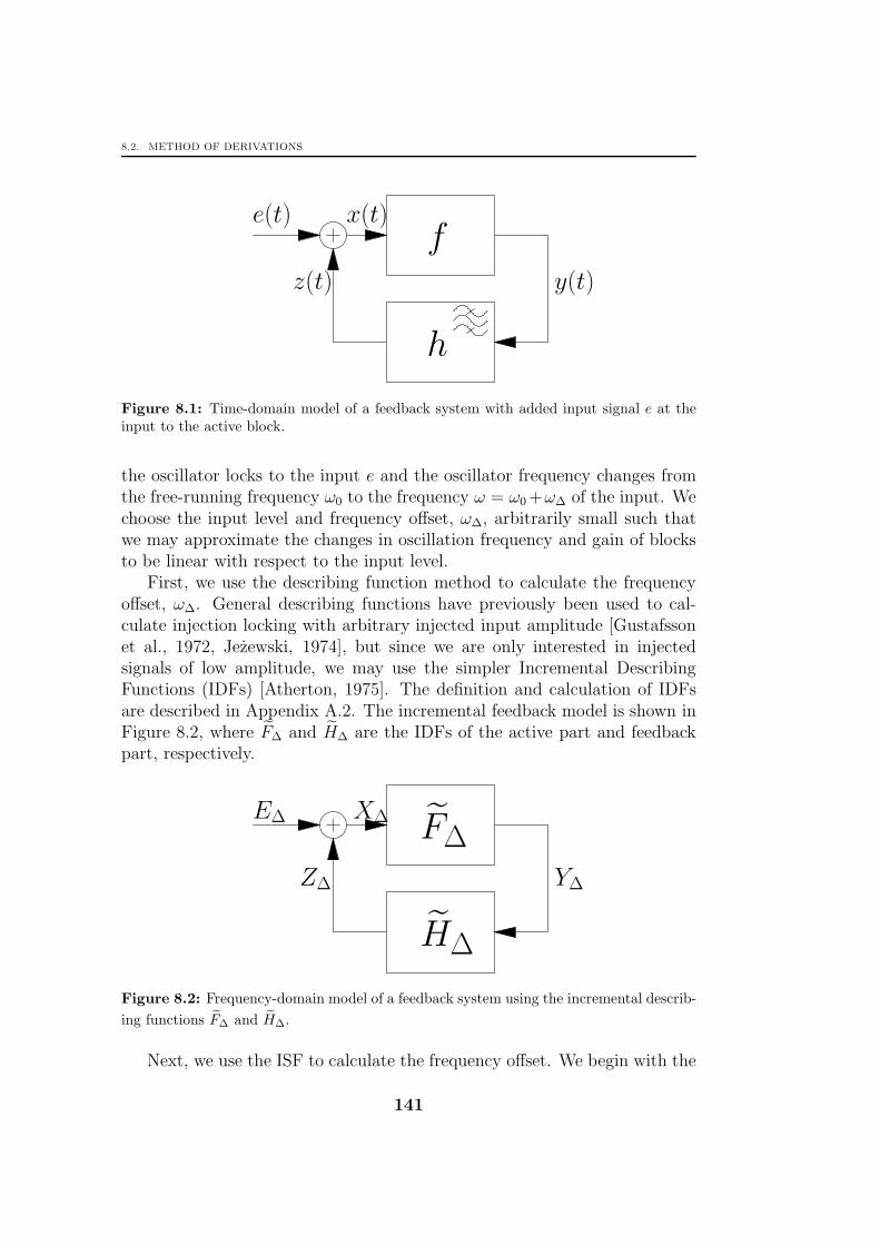
8.2. METHOD OF DERIVATIONS
h
y(t)
fx(t)
z(t)
e(t)
Figure 8.1: Time-domain model of a feedback system with added input signal e at theinput to the active block.
the oscillator locks to the input e and the oscillator frequency changes fromthe free-running frequency ω0 to the frequency ω = ω0 +ω∆ of the input. Wechoose the input level and frequency offset, ω∆, arbitrarily small such thatwe may approximate the changes in oscillation frequency and gain of blocksto be linear with respect to the input level.
First, we use the describing function method to calculate the frequencyoffset, ω∆. General describing functions have previously been used to cal-culate injection locking with arbitrary injected input amplitude [Gustafssonet al., 1972, Jezewski, 1974], but since we are only interested in injectedsignals of low amplitude, we may use the simpler Incremental DescribingFunctions (IDFs) [Atherton, 1975]. The definition and calculation of IDFsare described in Appendix A.2. The incremental feedback model is shown inFigure 8.2, where F∆ and H∆ are the IDFs of the active part and feedbackpart, respectively.
Z∆
X∆
Y∆
E∆
H∆
F∆
Figure 8.2: Frequency-domain model of a feedback system using the incremental describ-
ing functions F∆ and H∆.
Next, we use the ISF to calculate the frequency offset. We begin with the
141
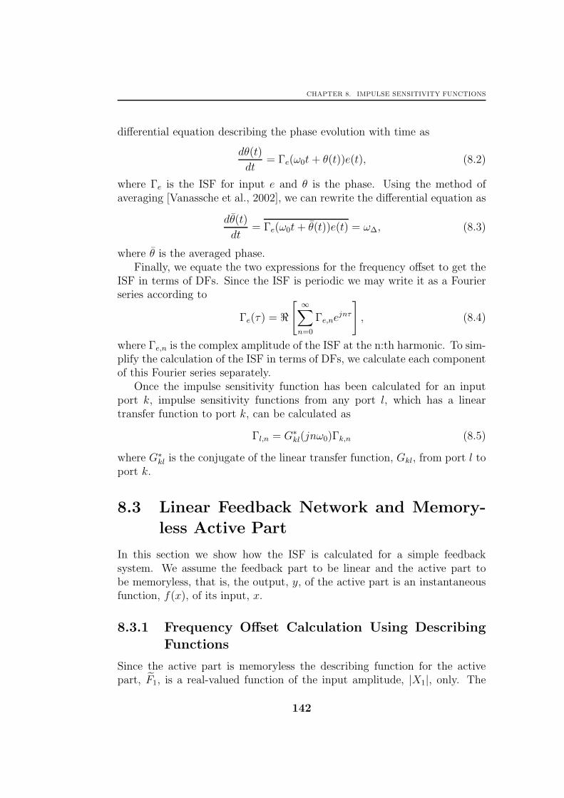
CHAPTER 8. IMPULSE SENSITIVITY FUNCTIONS
differential equation describing the phase evolution with time as
dθ(t)
dt= Γe(ω0t+ θ(t))e(t), (8.2)
where Γe is the ISF for input e and θ is the phase. Using the method ofaveraging [Vanassche et al., 2002], we can rewrite the differential equation as
dθ(t)
dt= Γe(ω0t+ θ(t))e(t) = ω∆, (8.3)
where θ is the averaged phase.Finally, we equate the two expressions for the frequency offset to get the
ISF in terms of DFs. Since the ISF is periodic we may write it as a Fourierseries according to
Γe(τ) = ℜ[ ∞∑
n=0
Γe,nejnτ
], (8.4)
where Γe,n is the complex amplitude of the ISF at the n:th harmonic. To sim-plify the calculation of the ISF in terms of DFs, we calculate each componentof this Fourier series separately.
Once the impulse sensitivity function has been calculated for an inputport k, impulse sensitivity functions from any port l, which has a lineartransfer function to port k, can be calculated as
Γl,n = G∗kl(jnω0)Γk,n (8.5)
where G∗kl is the conjugate of the linear transfer function, Gkl, from port l to
port k.
8.3 Linear Feedback Network and Memory-
less Active Part
In this section we show how the ISF is calculated for a simple feedbacksystem. We assume the feedback part to be linear and the active part tobe memoryless, that is, the output, y, of the active part is an instantaneousfunction, f(x), of its input, x.
8.3.1 Frequency Offset Calculation Using Describing
Functions
Since the active part is memoryless the describing function for the activepart, F1, is a real-valued function of the input amplitude, |X1|, only. The
142

8.3. LINEAR FEEDBACK NETWORK AND MEMORYLESS ACTIVE PART
gain of the feedback part, H1, is a function of the oscillation frequency onlyand may be written in an amplitude–phase form as
H1 = H(jω) = A(ω)ejα(ω) (8.6)
where H(jω) is the linear gain of the feedback part h, A is the amplitude gainand α is the phase shift of the feedback part. We also have that α(ω0) = 0
if F1 is positive and α(ω0) = π if F1 is negative, since the active part, f , is
memoryless and thereby H1 must be real.We now split the input disturbance to the active part, f , in an in-phase
and a quadrature-phase component relative to X1 according to
X∆,n = X(I)∆,n + jX
(Q)∆,n (8.7)
for any possible harmonic component at a frequency n times higher than thatof the fundamental. The incremental output, Y∆,n, from the active block isdescribed in the same way. Since the nonlinearity is memoryless, the phasesof X1 and Y1 must be equal equal or differ by π.
We proceed with the calculation of the fundamental output Y∆,1 as a func-tion of the input components X∆,n using Incremental Describing Functions(IDFs). The gains for the in-phase and the quadrature-phase components of
the IDFs, F∆n, are in general different and we have
F(I)∆,n =
∂Yn∂|X1|
= Fn +X1∂Fn∂|X1|
(8.8)
and, from Appendix A.2.2,F
(Q)∆,n = nFn. (8.9)
The in-phase output component of Y∆,1 may now be calculated as
Y(I)∆,1 =
∞∑
n=0
X(I)∆,nF
(I)∆,n (8.10)
and the quadrature-phase component as
Y(Q)∆,1 =
∞∑
n=0
X(Q)∆,nF
(Q)∆n =
∞∑
n=0
X(Q)∆,nnFn. (8.11)
We now consider the change in output from the linear feedback part, h,as a function of the change in oscillation frequency, ω, and get
∂H1
∂ω=
(1
A
∂A
∂ω+ j
∂α
∂ω
)H1 (8.12)
143

CHAPTER 8. IMPULSE SENSITIVITY FUNCTIONS
by taking the derivative of (8.6) with respect to ω. Since the feedback partis linear, the change in output from the feedback part, Z∆,1, due to a changein oscillation frequency is simply
Z∆,1 = ω∆∂H1
∂ω|Y1|. (8.13)
Using (8.13) and the property that the IDF of a linear part is simply thegain of that part, we calculate the in-phase and quadrature-phase componentsof the output from the feedback part, Z∆,1, as
Z(I)∆,1 = Y
(I)∆,1H1 + ω∆|Y1|
∂A
∂ω(8.14)
and
Z(Q)∆,1 = Y
(Q)∆,1 H1 + ω∆|X1|
∂α
∂ω, (8.15)
respectively, since we have assumed that the feedback part, h, filters out allharmonics but the fundamental.
At the summing point, we have
X(I)∆,1 = E
(I)∆,1 + Z
(I)∆,1, (8.16)
X(Q)∆,1 = E
(Q)∆,1 + Z
(Q)∆,1, (8.17)
X(I)∆,n = E
(I)∆,n, (8.18)
andX
(Q)∆,n = E
(Q)∆,n. (8.19)
Solving the equation system given by (8.10), (8.11), (8.14), (8.15), (8.16),(8.17), (8.18), and (8.19), we arrive at the frequency offset, ω∆, as a functionof the complex input amplitudes, E∆,n.
8.3.2 Frequency Offset Calculation Using the ISF
We now calculate the frequency offset using the ISF according to (8.3) as
ω∆ = Γe,0E∆,0 +∞∑
n=1
Γ(I)e,nE
(I)∆,n
2+
∞∑
n=1
Γ(Q)e,nE
(Q)∆,n
2, (8.20)
where we use that
Γ(I)e,n cos(n(ω0t+ θ))E
(I)∆,n cos(n(ω0t+ θ)) =
Γ(I)e,nE
(I)∆,n
2, (8.21)
144
8.3. LINEAR FEEDBACK NETWORK AND MEMORYLESS ACTIVE PART
Γ(Q)e,n sin(n(ω0t+ θ))E
(Q)∆,n sin(n(ω0t+ θ)) =
Γ(Q)e,nE
(Q)∆,n
2(8.22)
and where we also split the ISF in an in-phase and a quadrature-phase com-ponent relative to X1 according to
Γe,n = Γ(I)e,n + jΓ(Q)
e,n . (8.23)
8.3.3 Equating the Expressions for the Frequency Off-set
From the expressions for the frequency offset in terms of DFs from Sec-tion 8.3.1 and in terms of the ISF from Section 8.3.2, we may now calculatethe ISF in terms of DFs. The in-phase and quadrature-phase componentsof each harmonic, n, of the ISF may now be calculated separately using thefollowing method: First, set all components of E∆ but E
(I)∆,n equal to zero and
solve for Γ(I)e,n; and second, set all components of E∆ but E
(Q)∆,n equal to zero
and solve for Γ(Q)e,n . This decomposition is allowed since the equation system
is linear.
Using this method, we get the components of the ISF as
Γe,n = −j 2nFn
X1F1∂α∂ω
(8.24)
where we have taken the reference phase of x to be zero, i.e., X1 is real andpositive.
Defining the Q-factor of the feedback filter, h, according to Appendix E,to be
Q = −ω0
2
∂α
∂ω, (8.25)
we can rewrite the components of the ISF as
Γe,n = jnFnω0
X1F1Q. (8.26)
We see that the ISF is inversely proportional to the amplitude and to theQ-factor of the oscillator. We also notice that the sensitivity to disturbancesat higher harmonics is proportional to the harmonic content in the outputof the active part, f .
145

CHAPTER 8. IMPULSE SENSITIVITY FUNCTIONS
8.4 The General Case
When the feedback network is nonlinear, the derivations become more com-plicated. Therefore, only the DC and the fundamental components of theimpulse sensitivity function are derived here; these components are the mostimportant ones when calculating the phase noise.
The describing function for the fundamental component of the transferfunction for the feedback network may be written in an amplitude–phaseform as
H1(|X1|, ω) = A(|X1|, ω)ejα(|X1|,ω), (8.27)
where A and α are the amplitude gain and phase, respectively.In a similar way we may write the describing function for the active part
asF1(|X1|, ω) = B(|X1|, ω)ejζ(|X1|,ω), (8.28)
where B and ζ are the amplitude gain and phase, respectively.We see that both the amplitude and the phase are functions of the input
amplitude to the nonlinear blocks and the frequency of the input signal. Thefrequency dependency of the feedback network is obvious since it is designedto have a high frequency selectivity. The frequency dependence for the activepart may come from, for example, charge transport delay in transistors whenthey operate at high frequencies.
Below, we derive incremental gains for the active part, f , and all refer-ences to input and output should be taken with respect to the active part.We write the output of the active block, f , on an amplitude–phase formaccording to
Y1(|X1|, ω) = |Y1(|X1|, ω)|ej∠Y1(|X1|,ω) = F1X1. (8.29)
The amplitude of the output signal, |Y1|, is a function of the amplitude ofthe input signal, |X1|, and not of the input-signal phase, ∠X1. To simplifynotation, we henceforth omit the dependency on the input amplitude andfrequency.
The incremental gain of the active part, f , for an extra input signalorthogonal to that of the main input is
∂Y1
∂X(Q)1
= F1; (8.30)
that is, an orthogonal incremental input, X(Q)∆,1 , changes the input and out-
put phases by the same amount and does not affect the input and outputamplitudes as long as the incremental input signal amplitude is low.
146

8.4. THE GENERAL CASE
On the other hand, an extra input in phase with the main input to theactive part does change the input amplitude but not the input phase and theincremental gain is
∂Y1
∂X(I)1
=∂Y1
∂|X1|, (8.31)
which may be rewritten using (8.29) and (8.28) as
∂Y1
∂|X1|=∂|Y1|∂|X1|
ej∠Y1 + j∂∠Y1
∂|X1||Y1|ej∠Y1 =
(F
(I)∆,1
|Y1|+ j
∂ζ
∂|X1|
)Y1, (8.32)
where
F(I)∆,1 =
∂|Y1|∂|X1|
= B + |X1|∂B
∂|X1|. (8.33)
We see that we have one component in phase with Y1 and one in quadraturephase when an input in phase with X1 is applied at the input to the nonlinearactive part.
For an incremental DC input signal the conversion gain is
∂Y1
∂X0
=∂|Y1|∂X0
ej∠Y1 + j∂∠Y1
∂X0
|Y1|ej∠Y1 =
(F∆,0
|Y1|+ j
∂ζ
∂X0
)Y1, (8.34)
where
F∆,0 =∂|Y1|∂X0
= |X1|∂B
∂X0. (8.35)
For a DC input signal the incremental gain is
∂Y0
∂X0= F∆,DC . (8.36)
We also look at the change in output signal with respect to a shift ininput signal frequency and get
∂Y1
∂ω= X1
(∂B
∂ωejζ + j
∂ζ
∂ωBejζ
)=
(1
B
∂B
∂ω+ j
∂ζ
∂ω
)Y1. (8.37)
We split the input disturbance to the active part in an in-phase componentand a quadrature-phase component, relative to X1, according to
X∆,1 = X(I)∆,1 + jX
(Q)∆,1 (8.38)
and the output is described in the same way as
Y∆,1 = Y(I)∆,1 + jY
(Q)∆,1 , (8.39)
147

CHAPTER 8. IMPULSE SENSITIVITY FUNCTIONS
where in phase and quadrature phase is in relation to the signal Y1.Using (8.32), (8.34) and (8.37) we get the output in-phase component as
Y(I)∆,1 = X
(I)∆,1F
(I)∆,1 + ω∆|X1|
∂B
∂ω+X∆,0F∆,0, (8.40)
where we use that |Y1| = B|X1|.Using (8.30), (8.32), (8.34) and (8.37) we get the output quadrature com-
ponent as
Y(Q)∆,1 = X
(I)∆,1|Y1|
∂ζ
∂|X1|+X
(Q)∆,1B + ω∆|Y1|
∂ζ
∂ω+X∆,0|Y1|
∂ζ
∂X0. (8.41)
Using (8.36) we also have
Y∆,0 = X∆,0F∆,DC . (8.42)
We repeat the derivations above for the feedback part. The expressionsfor the feedback part, h, look similar to those for the active part, f . Wewrite the output of the feedback network in in-phase and quadrature-phasecomponents in relation to X1 as
Z∆,1 = Z(I)∆,1 + jZ
(Q)∆,1 (8.43)
and the in-phase component is calculated as
Z(I)∆,1 = Y
(I)∆,1H
(I)∆,1 + ω∆|Y1|
∂A
∂ω(8.44)
and the quadrature-phase component is calculated to be
Z(Q)∆,1 = Y
(I)∆,1|X1|
∂α
∂|Y1|+ Y
(Q)∆,1A+ ω∆|X1|
∂α
∂ω. (8.45)
The external disturbance to the oscillator is also divided in its orthogonalcomponents according to
E∆,1 = E(I)∆,1 + jE
(Q)∆,1, (8.46)
where in phase and quadrature phase is in relation to X1.We write the summation at the input to the active part as
X(I)∆,1 = E
(I)∆,1 + Z
(I)∆,1, (8.47)
X(Q)∆,1 = E
(Q)∆,1 + Z
(Q)∆,1 (8.48)
148

8.4. THE GENERAL CASE
and
X∆,0 = E∆,0 + Z∆,0. (8.49)
We can now calculate the frequency shift, ω∆, by solving the equationsystem made up of (8.40), (8.41), (8.44), (8.45), (8.47), (8.48) and (8.49).
Finally, we equate the expression for ω∆ we get by solving the equationsystem with the expression for ω∆ from Section 8.3.2 using the method inSection 8.3.3. We then get the components of the ISF as
Γx,0 = − 1(∂ζ∂ω
+ ∂α∂ω
) 1
1 − F∆,DCH∆,DC
(F∆,DC
∂α
∂Y0
+∂ζ
∂X0
+
+F∆,0
(H
(I)∆,1
∂ζ∂|X1| + ∂α
∂|Y1|
)+ F∆,DCH∆,0
(F
(I)∆,1
∂α∂|Y1| + ∂ζ
∂|X1|
)
1 − F(I)∆,1H
(I)∆,1
×
× 1
1 +|X1| ∂B
∂ω
“eH(I)
∆,1∂ζ
∂|X1|+ ∂α
∂|Y1|
”+|Y1| ∂A
∂ω
“eF (I)∆,1
∂α∂|Y1|
+ ∂ζ∂|X1|
”
“1− eF (I)
∆,1eH(I)
∆,1
”( ∂ζ
∂ω+ ∂α
∂ω)
(8.50)
and
Γx,1 = − 2
|X1|(∂ζ∂ω
+ ∂α∂ω
)
|X1|
(F
(I)∆,1
∂α∂|Y1| + ∂ζ
∂|X1|
)
1 − F(I)∆,1H
(I)∆,1
+ j
×
× 1
1 +|X1| ∂B
∂ω
“eH(I)
∆,1∂ζ
∂|X1|+ ∂α
∂|Y1|
”+|Y1| ∂A
∂ω
“eF (I)∆,1
∂α∂|Y1|
+ ∂ζ∂|X1|
”
“1− eF (I)
∆,1eH(I)
∆,1
”( ∂ζ
∂ω+ ∂α
∂ω)
. (8.51)
Noise entering at the output of the active part is calculated in a similarway to give the components of the ISF as
Γy,0 = − 1(∂ζ∂ω
+ ∂α∂ω
) 1
1 − F∆,DCH∆,DC
(H∆,DC
∂ζ
∂X0+∂α
∂Y0+
+H∆,0
(F
(I)∆,1
∂α∂|Y1| + ∂ζ
∂|X1|
)+ H∆,DCF∆,0
(H
(I)∆,1
∂ζ∂|X1| + ∂α
∂|Y1|
)
1 − F(I)∆,1H
(I)∆,1
×
× 1
1 +|Y1| ∂A
∂ω
“eF (I)∆,1
∂α∂|Y1|
+ ∂ζ∂|X1|
”+|X1| ∂B
∂ω
“eH(I)
∆,1∂ζ
∂|X1|+ ∂α
∂|Y1|
”
“1− eF (I)
∆,1eH(I)
∆,1
”( ∂ζ
∂ω+ ∂α
∂ω)
(8.52)
149

CHAPTER 8. IMPULSE SENSITIVITY FUNCTIONS
and
Γy,1 = − 2
|Y1|(∂ζ∂ω
+ ∂α∂ω
)
|Y1|
(H
(I)∆,1
∂ζ∂|X1| + ∂α
∂|Y1|
)
1 − F(I)∆,1H
(I)∆,1
+ j
×
× 1
1 +|Y1| ∂A
∂ω
“eF (I)∆,1
∂α∂|Y1|
+ ∂ζ∂|X1|
”+|X1| ∂B
∂ω
“eH(I)
∆,1∂ζ
∂|X1|+ ∂α
∂|Y1|
”
“1− eF (I)
∆,1eH(I)
∆,1
”( ∂ζ
∂ω+ ∂α
∂ω)
. (8.53)
8.4.1 Restricted Case
The expressions for the components of the ISF derived above are a bit compli-cated and somewhat hard to derive any insights from. We therefore simplifythem by assuming that ∂B
∂ω= 0 and ∂A
∂ω= 0, that is, the amplitude gains of
the blocks are independent of the frequency in the vicinity of the oscillationfrequency. We also assume that H∆,0 ≈ 0 and |F∆,DCH∆,DC| ≪ 1, that is,the conversion gain from low frequencies to the fundamental frequencies inthe feedback part is low and the low-frequency loop gain is much lower thanunity.
The expressions for the ISF components for noise entering at the inputto the active part become
Γx,0 = − 1(∂ζ∂ω
+ ∂α∂ω
)
F∆,DC
∂α
∂Y0+
∂ζ
∂X0+F∆,0
(H
(I)∆,1
∂ζ∂|X1| + ∂α
∂|Y1|
)
1 − F(I)∆,1H
(I)∆,1
(8.54)and
Γx,1 = − 2
|X1|(∂ζ∂ω
+ ∂α∂ω
)
|X1|
(F
(I)∆,1
∂α∂|Y1| + ∂ζ
∂|X1|
)
1 − F(I)∆,1H
(I)∆,1
+ j
. (8.55)
The expressions for the ISF components for noise entering at the outputof the active part become
Γy,0 = − 1(∂ζ∂ω
+ ∂α∂ω
)
H∆,DC
∂ζ
∂X0
+∂α
∂Y0
+H∆,DCF∆,0
(H
(I)∆,1
∂ζ∂|X1| + ∂α
∂|Y1|
)
1 − F(I)∆,1H
(I)∆,1
(8.56)and
Γy,1 = − 2
|Y1|(∂ζ∂ω
+ ∂α∂ω
)
|Y1|
(H
(I)∆,1
∂ζ∂|X1| + ∂α
∂|Y1|
)
1 − F(I)∆,1H
(I)∆,1
+ j
. (8.57)
150

8.4. THE GENERAL CASE
Sometimes it is more convenient to express the phase change as a functionof the output of a block instead of as a function of the input to the block. Inthe case for the feedback block we have the relationships
∂α
∂X0
= F∆,DC∂α
∂Y0
+F∆,0
(H
(I)∆,1
∂ζ∂|X1| + ∂α
∂|Y1|
)
1 − F(I)∆,1H
(I)∆,1
(8.58)
and∂α
∂|X1|= F
(I)∆,1
∂α
∂|Y1|(8.59)
and by using these relationships and the Q-value for the oscillator defined as
Q = −ω0
2
(∂α
∂ω+∂ζ
∂ω
), (8.60)
we can rewrite the components of the ISF as
Γx,0 =ω0
2Q
(∂α
∂X0+
∂ζ
∂X0
)(8.61)
and
Γx,1 =ω0
|X1|Q
|X1|
(∂α∂|X1| + ∂ζ
∂|X1|
)
1 − F(I)∆,1H
(I)∆,1
+ j
. (8.62)
A similar conversion can be done for the ISF at the output to the activeblock by using that
∂α
∂Y0
= H∆,DC∂α
∂X0
+H∆,DCF∆,0
(H
(I)∆,1
∂ζ∂|X1| + ∂α
∂|Y1|
)
1 − F(I)∆,1H
(I)∆,1
(8.63)
and∂α
∂|Y1|= H
(I)∆,1
∂α
∂|X1|(8.64)
and we get
Γy,0 =ω0
2Q
(H∆,DC
(∂ζ
∂X0+
∂α
∂X0
))(8.65)
and
Γy,1 =ω0
|Y1|Q
|Y1|H(I)
∆,1
(∂α∂|X1| + ∂ζ
∂|X1|
)
1 − F(I)∆,1H
(I)∆,1
+ j
. (8.66)
151

CHAPTER 8. IMPULSE SENSITIVITY FUNCTIONS
Comparing (8.61) and (8.65), we get
Γy,0 = H∆,DCΓx,0. (8.67)
Comparing (8.62) and (8.66), we get
ℜ[Γy,1] = H(I)∆,1ℜ[Γx,1] (8.68)
andℑ[Γy,1] = H1ℑ[Γx,1]. (8.69)
We define the AM-to-PM conversion factor, KAM−PM , as
KAM−PM =ℜ[Γy,1]
ℑ[Γy,1]. (8.70)
Using (8.66), we get the AM-to-PM conversion factor as
KAM−PM =|Y1|H(I)
∆,1
(∂α∂|X1| + ∂ζ
∂|X1|
)
1 − F(I)∆,1H
(I)∆,1
. (8.71)
8.5 Disturbances Entering Through the Ac-
tive and Feedback Parts
In many cases the noise does not enter as an additive component in thefeedback network, but is modulated by the active part as in Figure 8.3.Examples of such noise are noise from the amplitude-determining networkand noise from the biasing network.
To calculate the ISF for these noise sources, we have to calculate thetransfer function from the source, w, to the output of the active network, f ,in the IDF model of Figure 8.4. We assume that the fundamental componentof the ISF at the output of the active network, f , is the dominant one.
8.5.1 Linear Feedback Network and Memoryless Ac-tive Part
The following method is used to calculate the ISF for noise entering throughthe active part: The frequency shift, ω∆, can be calculated using either theISF for the input port w as
ω∆ = Γw,0W∆,0 +∞∑
n=1
Γ(I)w,nW
(I)∆,n
2+
∞∑
n=1
Γ(Q)w,nW
(Q)∆,n
2, (8.72)
152
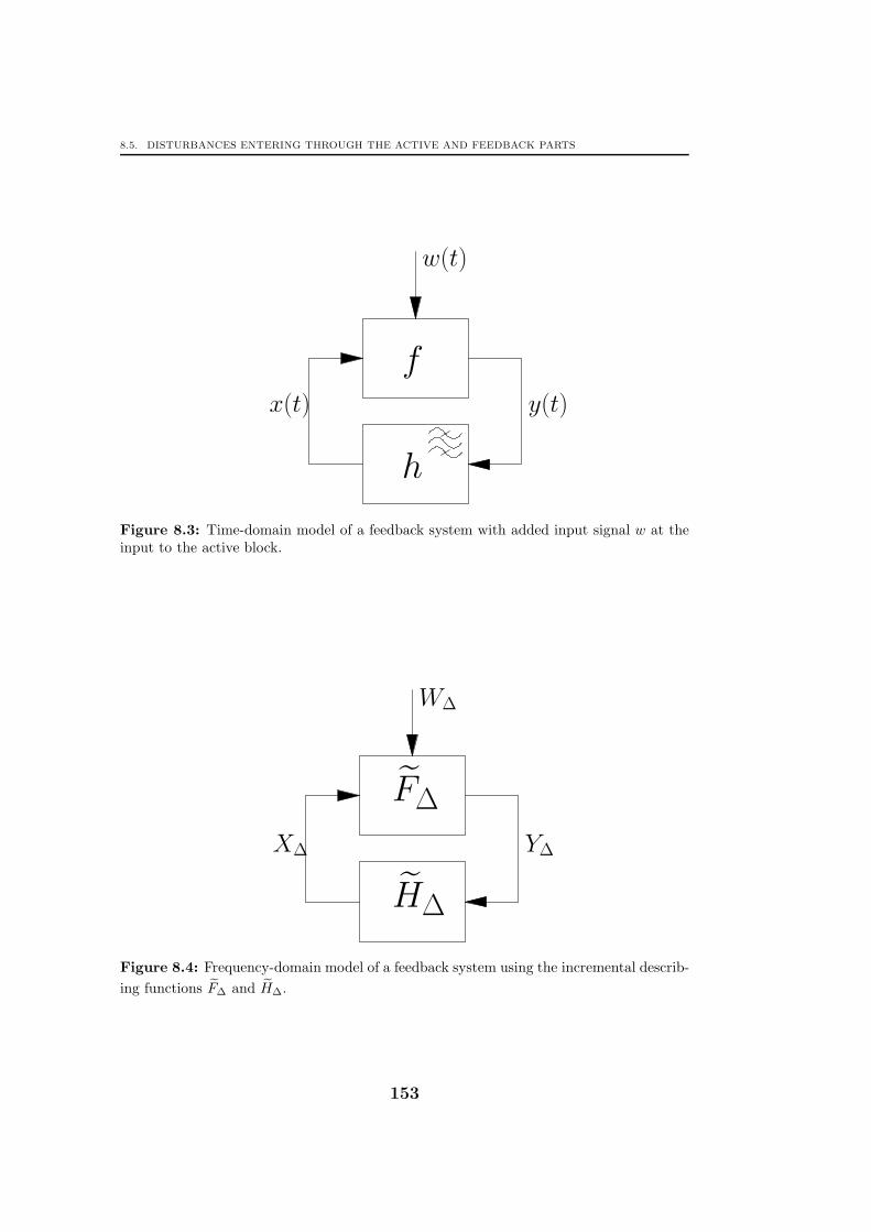
8.5. DISTURBANCES ENTERING THROUGH THE ACTIVE AND FEEDBACK PARTS
h
y(t)
fx(t)
w(t)
Figure 8.3: Time-domain model of a feedback system with added input signal w at theinput to the active block.
Y∆
H∆
F∆
X∆
W∆
Figure 8.4: Frequency-domain model of a feedback system using the incremental describ-
ing functions F∆ and H∆.
153

CHAPTER 8. IMPULSE SENSITIVITY FUNCTIONS
or using the ISF for the output port y as
ω∆ =Γ
(I)y,1Y
(I)∆,1
2+
Γ(Q)y,1 Y
(Q)∆,1
2, (8.73)
where we have assumed that the fundamental component of the ISF is dom-inant. Equating these two expression for the frequency offset, ω∆, gives usthe ISF for noise at signal w in terms of the ISF for noise at signal y.
The output of the active block, y, is a function both of the input, x, andthe bias signal, w, and can be written as
y = f(x, w). (8.74)
By Taylor expanding this expression with respect to w, we get the incre-mental output signal, y∆, as
y∆ =∂y(t)
∂ww∆, (8.75)
where w∆ is the incremental input signal. We denote the time-varying small-signal gain according to
d(t) =∂y(t)
∂w. (8.76)
Since the input signal, x(t), is a periodic signal with fundamental fre-quency ω0, we can write the small-signal gain, d(t), as a Fourier series ac-cording to
d(t) =
∞∑
n=0
Dn cos(nω0t). (8.77)
First, we insert a signal w∆ in phase and in quadrature phase in relationto the input signal, x, in (8.75), and use (8.76) and (8.77) to get the corre-sponding y∆. Second, we insert this expression for y∆ in (8.73) and the valuefor w∆ in (8.72) and equate these expressions for the frequency offset, whichfinally gives us the ISF for port w as
Γw,0 =ℜ[Γy,1]D1
2(8.78)
and
Γw,n =Γy,1Dn−1
2+
Γ∗y,1Dn+1
2. (8.79)
Rewriting this expression as
Γw,n =ℜ[Γy,1](Dn−1 +Dn+1)
2+ j
ℑ[Γy,1](Dn−1 −Dn+1)
2, (8.80)
we get the in-phase and quadrature-phase components of the ISF explicitly.
154

8.5. DISTURBANCES ENTERING THROUGH THE ACTIVE AND FEEDBACK PARTS
8.5.2 The General Case
We assume that high-frequency disturbances of w are filtered out so that theonly important component of the input, w, is the low-frequency part aroundDC, W∆,0.
The calculation is carried out in two steps: first, we calculate the con-version from the input, W∆,0, to the output of the active block, Y∆,1, andsecond, we calculate the ISF for noise entering through the input, w, usingthe ISF derived for noise at the output, y, in (8.53).
The conversion of low-frequency signals at the input to a fundamentalcomponent at the output is calculated using a Taylor expansion as
Y∆,1 = W∆,0∂Y1
∂W0
= W∆,0∂F1
∂W0
X1 = W∆,0
(∂B
∂W0
ejζ + jB∂ζ
∂W0
ejζ)X1,
(8.81)where we have used (8.28) and (8.29).
This expression may be rewritten as
Y∆,1 = W∆,0
(1
B
∂B
∂W0+ j
∂ζ
∂W0
)Y1 (8.82)
using (8.28) and we identify the in-phase component of the incremental out-put as
Y(I)∆,1 = W∆,0|Y1|
1
B
∂B
∂W0
(8.83)
and the quadrature-phase component of the incremental output as
Y(Q)∆,1 = W∆,0|Y1|
∂ζ
∂W0, (8.84)
where in phase and quadrature phase are taken relative to Y1.
The frequency shift, ω∆, can be calculated using either the ISF for theinput port, w, as
ω∆ = Γw,0W∆,0 (8.85)
or using the ISF for the output port, y, as
ω∆ =Γ
(I)y,1Y
(I)∆,1
2+
Γ(Q)y,1 Y
(Q)∆,1
2, (8.86)
assuming that the fundamental component of the ISF for noise entering atthe output of the active part is dominant.
155
CHAPTER 8. IMPULSE SENSITIVITY FUNCTIONS
Equating these two expressions for the frequency offset, we get the ISFfor port w as a function of the ISF for port y as
Γw,0 =|Y1|2
(Γ
(I)y,1
1
B
∂B
∂W0+ Γ
(Q)y,1
∂ζ
∂W0
), (8.87)
where we have used (8.83) and (8.84). Using (8.53) we get the wanted ISFas
Γw,0 = − 1(∂ζ∂ω
+ ∂α∂ω
)
|X1| ∂B∂W0
(H
(I)∆,1
∂ζ∂|X1| + ∂α
∂|Y1|
)
1 − F(I)∆,1H
(I)∆,1
+∂ζ
∂W0
×
× 1
1 +|Y1| ∂A
∂ω
“eF (I)∆,1
∂α∂|Y1|
+ ∂ζ∂|X1|
”+|X1| ∂B
∂ω
“eH(I)
∆,1∂ζ
∂|X1|+ ∂α
∂|Y1|
”
“1− eF (I)
∆,1eH(I)
∆,1
”( ∂ζ
∂ω+ ∂α
∂ω)
, (8.88)
which under the assumptions that ∂B∂ω
= 0 and ∂A∂ω
= 0 simplifies to
Γw,0 = − 1(∂ζ∂ω
+ ∂α∂ω
)
|X1| ∂B∂W0
(H
(I)∆,1
∂ζ∂|X1| + ∂α
∂|Y1|
)
1 − F(I)∆,1H
(I)∆,1
+∂ζ
∂W0
. (8.89)
Noise may also enter through the feedback part, h, via an input port, u,according to Figure 8.5. Signals entering to this passive part may for examplecome from a frequency tuning input port.
h
y(t)x(t)
u(t)
f
Figure 8.5: Time-domain model of a feedback system with added input signal u at theinput to the feedback block.
156
8.5. DISTURBANCES ENTERING THROUGH THE ACTIVE AND FEEDBACK PARTS
The ISF for noise entering through this input port, u, can be calculatedin a similar way to that of the port w. Carrying out these calculations, weget the ISF as
Γu,0 = − 1(∂ζ∂ω
+ ∂α∂ω
)
|Y1| ∂A∂U0
(F
(I)∆,1
∂α∂|Y1| + ∂ζ
∂|X1|
)
1 − F(I)∆,1H
(I)∆,1
+∂α
∂U0
×
× 1
1 +|X1| ∂B
∂ω
“eH(I)
∆,1∂ζ
∂|X1|+ ∂α
∂|Y1|
”+|Y1| ∂A
∂ω
“eF (I)∆,1
∂α∂|Y1|
+ ∂ζ∂|X1|
”
“1− eF (I)
∆,1eH(I)
∆,1
”( ∂ζ
∂ω+ ∂α
∂ω)
, (8.90)
which under the assumptions that ∂B∂ω
= 0 and ∂A∂ω
= 0 simplifies to
Γu,0 = − 1(∂ζ∂ω
+ ∂α∂ω
)
|Y1| ∂A∂U0
(F
(I)∆,1
∂α∂|Y1| + ∂ζ
∂|X1|
)
1 − F(I)∆,1H
(I)∆,1
+∂α
∂U0
. (8.91)
8.5.3 Other ISFs of Interest
In addition to the ISF calculations carried out in this chapter, we might wantto calculate the other frequency components of the ISF for noise enteringthrough the active part in the general case. These ISF components may beof interest if the phase shift of the active part is a function of the bias currentor voltage, and the bias has high-frequency noise associated with it.
157

CHAPTER 8. IMPULSE SENSITIVITY FUNCTIONS
158
Chapter 9Verification of Derived Expressions
T he verification of the expressions derived in this thesis is carried outstepwise in this chapter. Discussion on the verification of the designmethodology is given in Section 3.4.
First, I verify predicted performance against simulations where the ac-tive block is modeled as an ideal arc-tan nonlinearity in order to verify theapproximations done in the derivation of the Impulse Sensitivity Function(ISF) and the derivation of the phase noise. This verification is performedboth for linear and nonlinear feedback networks. Second, I verify the ISFsand the phase noise for an oscillator implemented with transistors. Finally,I verify predicted phase noise against measured data from many differenttopologies reported in literature.
9.1 Ideal Oscillator with Arc-tan Nonlinear-
ity
The ideal oscillator used in the first set of verifications is a negative-conductanceoscillator with a parallel LC tank, as shown in Figure 9.1.
The output current, y, as a function of the input voltage, x, is given by
y = f(x) =2ymaxπ
arctan
(πkx
2ymax
), (9.1)
and is plotted in Figure A.3 in Appendix A together with its derivative.
The component values are chosen to yield an oscillation frequency, f0,of 1.0 GHz and a Q-value of 10. Maximum output current, ymax, is 20 mAand we have a small-signal transconductance, k, of 30 mS. The values for
159

CHAPTER 9. VERIFICATION OF DERIVED EXPRESSIONS
f h
xy
y
L C R
Figure 9.1: Schematic for an ideal oscillator.
the passive components are: R = 100 Ω, L = 1.59154943 nH, and C =15.9154943 pF.
9.1.1 Linear Feedback Network
We begin by calculating the voltage amplitude for the fundamental frequencyat the input to the nonlinearity. From (A.54) in Appendix A we have thatthe input-voltage amplitude is given by
X1 =4ymaxR
π
√1 − 1
kR, (9.2)
where we have used that
H1 = H(jω0) = R. (9.3)
We proceed with the calculation of the other harmonics by using (A.50) and
Xn = H(jnω0)Yn (9.4)
where the parallel RLC tank has
H(jnω0) =H(jω0)
1 + jQn2−1n
=R
1 + jQn2−1n
. (9.5)
The calculated values for the complex voltage amplitudes of the harmonicsare given in Table 9.1 together with the simulated values and the magnitudeerrors in per cent. We note that the accuracy deteriorates for higher harmon-ics because the describing-function method neglects the presence of higherharmonics at the input of the nonlinearity.
160

9.1. IDEAL OSCILLATOR WITH ARC-TAN NONLINEARITY
Table 9.1: Complex amplitude of harmonics at input of nonlinearity.
calculated simulated unit error in mag.
X1 2079.2ej0 2079.4ej0 [mV] 0.01%X3 17.314ej1.608 17.254ej1.610 [mV] 0.35%X5 3.8495e−j1.550 3.7869e−j1.526 [mV] 1.65%X7 1.2833ej1.585 1.2270ej1.677 [mV] 4.59%X9 513.35e−j1.560 462.62e−j1.305 [mV] 9.88%
To examine how the Q-value affects the accuracy of the calculations, werepeat the calculations for different Q-values ranging from 1 to 50 and plotthe magnitude errors for the different harmonics in Figure 9.2. We note thatwe get small magnitude errors except when the Q-value is very low; especiallythe fundamental amplitude is well predicted.
We proceed with the calculation of the ISF for noise entering at the outputof the transconductance using (8.26) and (8.5) of Chapter 8 given as
Γy,n = jnFnω0H
∗(jnω0)
X1F1Q, (9.6)
where Fn is the describing function for the active part, f , given in (A.50) andH(jnω0) is given by (9.5). The different calculated frequency components ofthe ISF are given in Table 9.2 together with simulated results and resultingerrors for the amplitude of the components in per cent.
The ideal oscillator was simulated using transient simulation with a noiseimpulse injected and the resulting phase error was extracted when the oscil-lator had eventually reached steady-state, as proposed by Hajimiri and Lee[Hajimiri and Lee, 1998].
Table 9.2: Frequency components of the impulse sensitivity function.
calculated simulated unit error in mag.
Γ1 30219ej1.571 30408ej1.565 [Mrad/C] 0.62%Γ3 754.95e−j0.037 752.79e−j0.035 [Mrad/C] 0.29%Γ5 279.75ej3.121 278.76ej3.127 [Mrad/C] 0.36%Γ7 130.56e−j0.015 137.78e−j0.023 [Mrad/C] 5.24%Γ9 67.150ej3.130 66.903ej3.234 [Mrad/C] 0.37%
We also want to examine how different Q-values affect the approxima-tion of the ISF, so we simulate the oscillator with different Q-values ranging
161

CHAPTER 9. VERIFICATION OF DERIVED EXPRESSIONS
100
101
102
10−4
10−3
10−2
10−1
100
101
102
Relative error for amplitudes as function of Q−value for different harmonics
Q−value
Rel
ativ
e er
ror
[%]
1:st harm3:rd harm5:th harm7:th harm9:th harm
Figure 9.2: Relative error for amplitudes as function of Q-value for different harmonics.
from 1 to 50 and plot the relative resulting errors in per cent for the calcu-lated magnitudes of the ISF components when compared to the simulatedcounterparts in Figure 9.3.
The fundamental frequency component has an error of less than 1% exceptwhen the Q-value is extremely low. Higher frequency components may haveerrors in the order of 10%, especially for low Q-values.
We finally pay our attention to the phase noise, which is what we reallyis after. We assume that the noise spectral density of the active part isproportional to the small-signal transfer conductance according to
Sy,f(ω, t) = 4kBTγ|f ′(X1 cos(ω0t))| (9.7)
where γ is a proportionality constant and f ′(x) is used to denote the deriva-tive of f(x) with respect to x. From (7.76) in Chapter 7 we have that
L[ωm] ≈ kBTR(1 + γ)
X21Q
2
ω20
ω2m
, (9.8)
162

9.1. IDEAL OSCILLATOR WITH ARC-TAN NONLINEARITY
100
101
102
10−1
100
101
102
Relative error for ISF as function of Q−value for different harmonics
Q−value
Rel
ativ
e er
ror
[%]
1:st harm3:rd harm5:th harm7:th harm9:th harm
Figure 9.3: Relative error for frequency components of the ISF as function of Q-value.
where we have used that the noise factor, F , is approximately given by
F ≈ 1 + γ. (9.9)
We simulate the phase noise at an offset of 100 kHz with γ being 2/3 and1 and give the simulated values together with those we get from (9.8) inTable 9.3. As seen, we have excellent agreement between predicted andsimulated phase-noise performance.
Table 9.3: Phase noise @ 100 kHz offset.
calculated simulated unit
γ = 2/3 −127.97 −127.96 [dBc/Hz]γ = 1 −127.17 −127.17 [dBc/Hz]
We also want to know how different Q-values affect the accuracy of ourphase-noise calculation, so we plot the difference between the simulated and
163

CHAPTER 9. VERIFICATION OF DERIVED EXPRESSIONS
calculated phase noise in Figure 9.4 for Q-values ranging from 1 to 50 withγ = 1. Even for a Q-value as low as 3, we have an error in calculated phasenoise of less than 0.05 dB.
100
101
102
−0.05
0
0.05
0.1
0.15
0.2
0.25
0.3
0.35
0.4Error for phase noise at 100 kHz offset as function of Q−value
Q−value
Err
or [d
B]
Figure 9.4: Error for phase noise at 100 kHz offset as function of Q-value.
Correction to Oscillation Frequency
Since we have neglected all higher harmonics of the signal at the output ofthe active block, we now consider them to be input signals to the system andcalculate the frequency shift assuming that this additional signal, y∆, can beconsidered small. This additional signal is given by
y∆(t) = ℜ[ ∞∑
n=2
Ynejn(ω0+ω∆)t
]= ℜ
[ ∞∑
n=2
FnX1ejn(ω0+ω∆)t
]. (9.10)
The frequency shift may now be calculated as
ω∆ = Γy((ω0 + ω∆)t)y∆(t), (9.11)
164

9.1. IDEAL OSCILLATOR WITH ARC-TAN NONLINEARITY
where the over-line is used to denote time averaging and the ISF, Γy, is givenby
Γy((ω0 + ω∆)t) = ℜ[ ∞∑
n=0
Γy,nejn(ω0+ω∆)t
], (9.12)
where
Γy,n = jnFnω0H
∗(jnω0)
X1F1Q(9.13)
from (9.6).Performing the averaging, we get the frequency shift as
ω∆ =1
2
∞∑
n=2
ℜ[Γy,n]Yn, (9.14)
where we have used that Yn must be real since the active part is memoryless.We also have that
ℜ[Γy,n] =nFnω0ℑ[H(jnω0)]
X1F1Q. (9.15)
For a second order system we have
ℑ[H(jnω0)] = −H(jω0)Q(n− 1
n)
1 +Q2(n− 1n)2, (9.16)
which finally gives us
∆ω = − ω0
2Q2
∞∑
n=2
n2(n2 − 1)
n2/Q2 + (n2 − 1)2
F 2n
F 21
. (9.17)
This expression is equal to that given by Groszkowski using the method ofreactive power balance of harmonics [Groszkowski, 1964].
We plot the frequency shift in Figure 9.5, both simulated and calculatedfrom (9.17) using the first nine harmonics only, i.e., n ≤ 9.
Noise from Two-Port Feedback Network
In this section we compare the phase-noise performance for two oscillatorswith two different transimpedance networks having the same transfer func-tion, Z21, and input impedance, Z11, but different output impedance, Z22.The first oscillator, shown in Figure 9.6, has a capacitive voltage divisionand the second oscillator, shown in Figure 9.7, has a resistive voltage divi-sion. We choose the component values such that the oscillation frequency is
165
CHAPTER 9. VERIFICATION OF DERIVED EXPRESSIONS
100
101
102
−3.5
−3
−2.5
−2
−1.5
−1
−0.5
0Relative frequency shift
Q−value
Rel
ativ
e fr
eque
ncy
shift
[%]
simulatedcalculated
Figure 9.5: Relative frequency shift as function of Q-value.
1 GHz in both cases and the voltage amplitude is equal at the output of theactive block. Consequently, the small-signal transconductance at startup, k,is chosen to be 60 mS. The voltage division factor is equal to 1/2.
The phase-noise performance is summarized in Table 9.4. The main dif-ference between the two oscillators is that only the transimpedance networkwith the capacitive voltage division fulfills the approximation Z11Z22 ≈ Z2
21.In addition to this difference, the real part of the output impedance at mul-tiples of the fundamental frequency is much higher for the transimpedancenetwork with the resistive voltage division.
Table 9.4: Phase noise @ 100 kHz offset.
C div. R div. approx. calc. unit
feedback only −130.18 −125.71 −130.18 [dBc/Hz]active only −127.17 −127.17 −127.17 [dBc/Hz]total −125.41 −123.37 −125.41 [dBc/Hz]
166
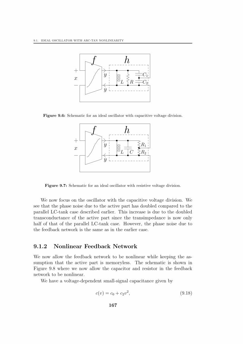
9.1. IDEAL OSCILLATOR WITH ARC-TAN NONLINEARITY
f h
xy
y
L C2R
C1
Figure 9.6: Schematic for an ideal oscillator with capacitive voltage division.
f h
xy
y
L C
R1
R2
Figure 9.7: Schematic for an ideal oscillator with resistive voltage division.
We now focus on the oscillator with the capacitive voltage division. Wesee that the phase noise due to the active part has doubled compared to theparallel LC-tank case described earlier. This increase is due to the doubledtransconductance of the active part since the transimpedance is now onlyhalf of that of the parallel LC-tank case. However, the phase noise due tothe feedback network is the same as in the earlier case.
9.1.2 Nonlinear Feedback Network
We now allow the feedback network to be nonlinear while keeping the as-sumption that the active part is memoryless. The schematic is shown inFigure 9.8 where we now allow the capacitor and resistor in the feedbacknetwork to be nonlinear.
We have a voltage-dependent small-signal capacitance given by
c(v) = c0 + c2v2, (9.18)
167

CHAPTER 9. VERIFICATION OF DERIVED EXPRESSIONS
f h
xy
y
L C R
Figure 9.8: Schematic for an ideal oscillator with nonlinear feedback network.
and a resistance with the I–V characteristics given by
v(i) = r1i+ r3i3. (9.19)
From (6.10) in Chapter 6 we have that
C(X1) = C0(X1) −1
2C2(X1) = c0 +
1
4c2X
21 . (9.20)
Keeping the large-signal capacitance, C, constant and assuming that
c0 = kCC, (9.21)
where kC is a constant, we get
c2 =4(C − c0)
X21
=4(1 − kC)
X21
C. (9.22)
In a similar way we can calculate the large-signal resistance as
H1 = R = r1 +3
4r3Y
21 (9.23)
Keeping the large-signal resistance, R, constant and assuming that
r1 = kRH1, (9.24)
where kR is a constant, we get
r3 =4(H1 − r1)
3Y 21
=4(1 − kR)
3Y 21
H1. (9.25)
168

9.1. IDEAL OSCILLATOR WITH ARC-TAN NONLINEARITY
We now calculate the Impulse Sensitivity Function (ISF) given by (8.66)as
Γy,1 =ω0
Y1Q
(Y1H
(I)∆,1
∂α∂X1
1 − F(I)∆,1H
(I)∆,1
+ j
)(9.26)
where we have set ∂ζ∂X1
= 0 since the active block is memoryless.We also have that
∂α
∂X1=∂α
∂C
∂C
∂X1= −2Q(1 − kC)
X1, (9.27)
where we have used that
∂C
∂X1
=C2
X1
=1
2c2X1 =
2(1 − kC)C
X1
(9.28)
and∂α
∂C= −Q
C. (9.29)
The Incremental Describing Function (IDF) for the feedback network isgiven by
H(I)∆,1 =
∂X1
∂Y1=∂(Y1H1)
∂Y1= r1 +
9
4r3Y
21 = H1(3 − 2kR), (9.30)
where we have used (9.23).From (A.55) in Appendix A we have that
F(I)∆,1 =
∂Y1
∂X1=
F1√1 +
(πkX1
2ymax
)2. (9.31)
Inserting (9.27), (9.30) and (9.31) in (9.26), we get
Γy,1 =ω0
Y1Q
−2Q(1 − kC)(3 − 2kR)
1 − 3−2kRr1+( πkX1
2ymax)2
+ j
. (9.32)
The fundamental component of the ISF was simulated for different valuesof kC and kR in Table 9.5 and compared to the calculated value we get from(9.32).
We see that the error in predicted ISF increases with increasing nonlin-earity in the feedback network. The amount of higher harmonics increases
169
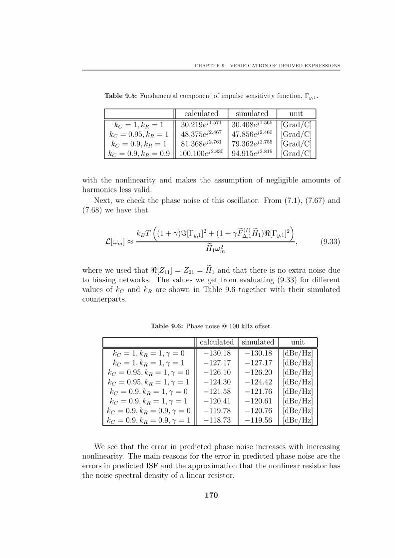
CHAPTER 9. VERIFICATION OF DERIVED EXPRESSIONS
Table 9.5: Fundamental component of impulse sensitivity function, Γy,1.
calculated simulated unit
kC = 1, kR = 1 30.219ej1.571 30.408ej1.565 [Grad/C]kC = 0.95, kR = 1 48.375ej2.467 47.856ej2.460 [Grad/C]kC = 0.9, kR = 1 81.368ej2.761 79.362ej2.755 [Grad/C]kC = 0.9, kR = 0.9 100.100ej2.835 94.915ej2.819 [Grad/C]
with the nonlinearity and makes the assumption of negligible amounts ofharmonics less valid.
Next, we check the phase noise of this oscillator. From (7.1), (7.67) and(7.68) we have that
L[ωm] ≈kBT
((1 + γ)ℑ[Γy,1]
2 + (1 + γF(I)∆,1H1)ℜ[Γy,1]
2)
H1ω2m
, (9.33)
where we used that ℜ[Z11] = Z21 = H1 and that there is no extra noise dueto biasing networks. The values we get from evaluating (9.33) for differentvalues of kC and kR are shown in Table 9.6 together with their simulatedcounterparts.
Table 9.6: Phase noise @ 100 kHz offset.
calculated simulated unit
kC = 1, kR = 1, γ = 0 −130.18 −130.18 [dBc/Hz]kC = 1, kR = 1, γ = 1 −127.17 −127.17 [dBc/Hz]kC = 0.95, kR = 1, γ = 0 −126.10 −126.20 [dBc/Hz]kC = 0.95, kR = 1, γ = 1 −124.30 −124.42 [dBc/Hz]kC = 0.9, kR = 1, γ = 0 −121.58 −121.76 [dBc/Hz]kC = 0.9, kR = 1, γ = 1 −120.41 −120.61 [dBc/Hz]kC = 0.9, kR = 0.9, γ = 0 −119.78 −120.76 [dBc/Hz]kC = 0.9, kR = 0.9, γ = 1 −118.73 −119.56 [dBc/Hz]
We see that the error in predicted phase noise increases with increasingnonlinearity. The main reasons for the error in predicted phase noise are theerrors in predicted ISF and the approximation that the nonlinear resistor hasthe noise spectral density of a linear resistor.
170

9.1. IDEAL OSCILLATOR WITH ARC-TAN NONLINEARITY
9.1.3 Nonlinear Feedback Network and Diode Limit-ing
We saw in the last section that a nonlinear feedback network may increasethe phase noise substantially, mainly due to the AM-to-PM conversion mech-anism. This increase in phase noise comes from the real part of (9.26) and wesee that to decrease this extra noise, we can introduce an amplitude limitingfunction. By introducing diode limiting, we get H
(I)∆,1 ≪ H1.
f
xy
y
L C R
h
Figure 9.9: Schematic for an ideal oscillator with nonlinear feedback network with am-plitude control.
The diodes used during simulations are ideal with no series resistanceor parallel capacitance. We may now approximate the oscillation amplitudeusing
X1,nonlin ≈ 2VT ln
(ymaxIS
)≈ 1.35 V (9.34)
where IS=0.1 pA for the chosen diodes and the 2 comes from the number ofseries-connected diodes.
Instead of performing the full phase-noise calculation, we can get an ap-proximate value for the phase noise by neglecting the AM-to-PM conversionand use
L[ωm] ≈ Llin[ωm]X3
1,lin
X31,nonlin
, (9.35)
where Llin is the phase noise for an oscillator with linear feedback network,X1,lin is the voltage amplitude for an oscillator with a linear feedback net-work without limiting and X1,nonlin is the voltage amplitude with limiting.The cube comes from the fact that we decrease the Q-value and the inputimpedance to the feedback network, where the phase noise is inversely pro-portional to the squared Q-value and inversely proportional to the inputimpedance. This expression gives the phase noise as −121.54 dBc/Hz at
171

CHAPTER 9. VERIFICATION OF DERIVED EXPRESSIONS
100 kHz offset. This expression will give a slight overestimate of the phasenoise since the input-current amplitude to the feedback network, Y1, is some-what lower with this new lower voltage amplitude, X1,nonlin, and the noiseof the diodes are less than those of a corresponding resistor. The simulatedvalues for the phase noise are given in Table 9.7 with γ = 1. We see that
Table 9.7: Phase noise @ 100 kHz offset.
phase noise amplitude
kC = 1 −122.19 [dBc/Hz] 1.340 VkC = 0.95 −121.96 [dBc/Hz] 1.349 VkC = 0.9 −121.68 [dBc/Hz] 1.358 V
the phase noise is much less dependent on the nonlinearities in the feedbacknetwork compared to the unregulated case.
9.1.4 Nonlinear Feedback Network and Automatic Am-plitude Control
Another amplitude control can be achieved by measuring the oscillation volt-age amplitude using a peak detector, comparing it with a reference voltage,and regulating the bias current to the active part according to the blockdiagram of Figure 9.10. The amplitude regulation gives |F (I)
∆,1H(I)∆,1| ≫ 1 in
(9.26).The values for the differential diode peak detector are: RP = 4 kΩ,
CP = 400 pF, and the gain for the bias control is Gm = 100 mS. Thesevalues give a loading resistance of R ≈ 2 kΩ using (5.14), which gives anegligible load compared to the tank resistance of approximately 100 Ω.
We choose the reference voltage, xref , to get an approximate voltagelimited amplitude of X1,nonlin = 1.4 V. The phase noise can be approximatedas
L[ωm] ≈ Llin[ωm]X2
1,lin
X21,nonlin
, (9.36)
where Llin is the phase noise for an oscillator with linear feedback network,X1,lin is the voltage amplitude for an oscillator with a linear feedback networkwithout limiting and X1,nonlin is the voltage amplitude with limiting. Thesquare comes from the fact that we decrease the input amplitude to the feed-back network, where the phase noise is inversely proportional to the squaredinput amplitude. This expression gives the phase noise as −123.74 dBc/Hzat 100 kHz offset. Simulated values for the phase noise of this oscillator are
172

9.2. SIMULATION OF TRANSISTOR TOPOLOGY
f h
xy
y
L C R
xref
Gm
Σ
Figure 9.10: Schematic for an ideal oscillator with nonlinear feedback network withamplitude control.
Table 9.8: Phase noise @ 100 kHz offset.
phase noise amplitude
kC = 1 −123.48 [dBc/Hz] 1.388 VkC = 0.95 −123.19 [dBc/Hz] 1.398 VkC = 0.9 −122.60 [dBc/Hz] 1.409 V
given in Table 9.8 with γ = 1. We see that the phase noise is much lessdependent on the nonlinearities in the feedback network compared to theunregulated case.
9.2 Simulation of Transistor Topology
We now simulate a Colpitts oscillator using electronic building-blocks. Thecomponent models used are ideal unless otherwise stated, e.g. no seriesresistances, parasitic capacitances or delays. The reason for using idealizedbehavior is that we here want to know the errors in approximations donewhen deriving the expressions for phase noise, not the errors in componentmodels.
This oscillator is not designed to be optimal in any way – it is only de-
173

CHAPTER 9. VERIFICATION OF DERIVED EXPRESSIONS
signed to check the expressions derived for the design methodology, especiallythose for the phase noise. The essentials for the oscillator are shown in Fig-ure 9.11 where we see that the active part is made up of a bipolar transistorand the feedback network is a CLC transimpedance network.
−
+
−
+iC
LvCEvBE
f
CA CC
h
Figure 9.11: Schematic.
We assume that the capacitors have very high Q-values and that theinductor has a Q-value of 100. We have a supply voltage, VCC , of 10 V and asupply current, IEE, of 1 mA. The transistor has a β of 100 and the oscillationfrequency, f0, is 1 MHz. We assume that the base series resistance, rbb, isnegligible, which in this case means that it is much lower than 1 Ω.
The values for the feedback network are chosen such that we get thevoltage amplitudes at the input to the active network as |Vbe,1| = 2.5 V andat the output of the active network as |Vce,1| = 5 V. This implies that Z11 =−2Z21. We also have that the output-current amplitude is |Ic,1| ≈ 2IEE. Theinput impedance to the feedback network is given by
Z11 = −Vce,1Ic,1
(9.37)
and the transimpedance is given by
Z21 = −Vbe,1Ic,1
. (9.38)
The capacitances are given as CA = C/(1 − n) and CC = C/n, wheren = 1/3 in this case. We can now calculate the values for the capacitancesfrom
C =Qn(1 − n)
ω0|Z21|(9.39)
174

9.2. SIMULATION OF TRANSISTOR TOPOLOGY
and the inductance as
L =1
ω20C
. (9.40)
From these design values, we can calculate the power efficiency as
η ≈ − Vce,1Ic,12VCCIEE
=1
2(9.41)
and the noise factor as
F ≈ 1 + γZ11
|Z21|= 2, (9.42)
where we have γ = 1/2 for bipolar transistors.We can now calculate the resulting phase noise as
L[ωm] ≈ kBTF
2PDCQ2η
ω20
ω2m
, (9.43)
where PDC = VCCIEE is the power consumption.The schematic for the biased oscillator is given in Figure 9.12. The resistor
R models the losses in the inductor L. The bias voltage VBB is chosen to be1.4 V to always have a positive voltage over the current bias source, IEE .
VCC
L
R
VBB IEE
CA
CC
Figure 9.12: Schematic.
Simulating this schematic, we get the voltage amplitudes as |Vc,1| = 7.28 Vand |Ve,1| = 2.43 V to be compared to the calculated values of |Vc,1| = 7.50 Vand |Ve,1| = 2.50 V. The simulated phase noise is −140.49 dBc/Hz at 100 Hzoffset compared to the calculated value of −140.82 dBc/Hz using (9.43). The
175

CHAPTER 9. VERIFICATION OF DERIVED EXPRESSIONS
peak emitter current is simulated to be 23.95 mA compared to the calculatedvalue of 24.58 mA using (C.23).
Adding a base resistance rb of 2 Ω increases the phase noise. The newnoise factor is given by
F ≈ 1 + γZ11
|Z21|+
4
9
rbZ11
Z211
Z221
( |Vbe,1|VT
) 32
, (9.44)
where we have used (7.23) and (C.24) for the additional term. The new valuefor the noise factor is 3.35. The new simulated phase noise is −138.36 dBc/Hzat 100 Hz offset compared to the calculated value of = −138.57 dBc/Hz.
We now look at the influence of the biasing network on the phase noiseof the implemented oscillator. The schematic is given in Figure 9.13. Theresistor RE is chosen such that the voltage drop across this resistor is 300 mV,which gives a value of 300 Ω. The capacitor, CE, filters out most of the noisecoming from the left side of the current mirror, so the bias noise is mainlymade up of the noise from the transistor and resistor acting as a currentsource. Since the voltage drop over RE is much higher than the thermalvoltage, VT , the noise current from the bias network is approximately thatof the resistor, RE , alone.
VCC
L
R
VBB
RE
VCC
IEE
CERE
CA
CC
Figure 9.13: Schematic.
176
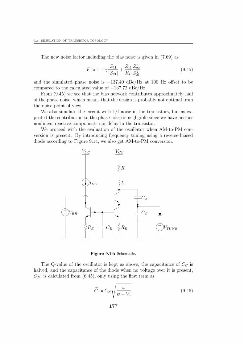
9.2. SIMULATION OF TRANSISTOR TOPOLOGY
The new noise factor including the bias noise is given in (7.69) as
F ≈ 1 + γZ11
|Z21|+Z11
RE
Z222
Z221
(9.45)
and the simulated phase noise is −137.40 dBc/Hz at 100 Hz offset to becompared to the calculated value of −137.72 dBc/Hz.
From (9.45) we see that the bias network contributes approximately halfof the phase noise, which means that the design is probably not optimal fromthe noise point of view.
We also simulate the circuit with 1/f noise in the transistors, but as ex-pected the contribution to the phase noise is negligible since we have neithernonlinear reactive components nor delay in the transistor.
We proceed with the evaluation of the oscillator when AM-to-PM con-version is present. By introducing frequency tuning using a reverse-biaseddiode according to Figure 9.14, we also get AM-to-PM conversion.
VCC
L
R
VBB
RE
VCC
IEE
CERE VTUNE
CA
CC
Figure 9.14: Schematic.
The Q-value of the oscillator is kept as above, the capacitance of CC ishalved, and the capacitance of the diode when no voltage over it is present,CN , is calculated from (6.45), only using the first term as
C ≈ CN
√ψ
ψ + V0, (9.46)
177

CHAPTER 9. VERIFICATION OF DERIVED EXPRESSIONS
where V0 = VTUNE − Ve,0, with the DC potential at the emitter, Ve,0, asapproximately 3 V, and the built-in diode potential, ψ, equal to 1 V. Weassume that we want an oscillation frequency of 1 MHz when VTUNE = 10 Vand consequently C must be half of the value of CC calculated above at thisvoltage. Simulating the oscillator, we get the voltage amplitudes as |Vc,1| =7.15 V and |Ve,1| = 2.37 V and the oscillation frequency as 998.66 kHz.
We now calculate the AM-to-PM conversion, KAM−PM , given in (6.28)as
KAM−PM ≈ |X1|1 − F
(I)∆,1H
(I)∆,1
H(I)∆,1
H1
∂α
∂|X1|, (9.47)
where from (6.29) we have that
∂α
∂|X1|= − ∂α
∂ω0
∂ω0
∂C
∂C
∂V1
∂V1
∂|X1|, (9.48)
where V1 is the voltage amplitude over the varactor. In this topology, we seethat V1 = X1. From (6.32) we have
∂α
∂ω0
≈ −2Q
ω0
(9.49)
and from (6.22) we have
∂ω0
∂C=∂ω0
∂C
∂C
∂C≈ − ω0
2C
∂C
∂C, (9.50)
where
C =CA(CC + C)
CA + CC + C(9.51)
and consequently∂C
∂C=
C
CC + C− C
CA + CC + C. (9.52)
Combing these expressions and assuming that |F (I)∆,1H
(I)∆,1| ≪ 1 and
eH(I)∆,1
eH1≈
1, we get
KAM−PM ≈ −QC2
C
∂C
∂C, (9.53)
where we also used from (6.33) that
∂C
∂V1
=C2
V1
, (9.54)
178

9.2. SIMULATION OF TRANSISTOR TOPOLOGY
where C2 is defined in Section 6.2. Inserting values, we get KAM−PM =−2.53.
We now focus on the phase noise due to white noise. Since the AM-to-PM conversion is high, we cannot assume that the low-frequency noisecontribution to the phase noise is negligible.
The new noise factor is given by
F ≈ 1 + γZ11
|Z21|+Z11
RE
Z222
Z221
+K2AM−PM
(1 + γ|G(I)
∆,1|Z11 +Z11
RE
Z222
Z221
+ 4Z11
RE
),
(9.55)
where KAM−PM is the AM-to-PM conversion and G(I)∆,1 is the incremental
large-signal transconductance of the transistor, which we assume is smallenough to be negligible since the transistor operates in Class C. The lastterm in the expression for the noise factor is the contribution from the tworesistors RE , since noise from neither of them are filtered out by capacitorCE at low frequencies. Inserting values gives us a noise factor of staggering237.4.
We now get the calculated phase noise as −120.08 dBc/Hz at 100 Hzoffset to be compared to the simulated value of −119.39 dBc/Hz at 100 Hzoffset. We see that the phase noise performance of the oscillator is extremelypoor due to the high AM-to-PM conversion due to the diode varactor incombination with the low-frequency noise due to the biasing network.
We proceed with the calculation of phase noise due to 1/f noise. Thetransistors have a 1/f noise factor K1/f = 5 fA2/Hz, corresponding to a noisecorner frequency of approximately 160 Hz. The phase noise due to 1/f noiseis given in (7.95) as
L[ωm] =2π(K1/f,f +K1/f,b)IEE
8Q2
(KAM−PM
1
B
∂B
∂IEE+
∂ζ
∂IEE
)2ω2
0
ω3m
. (9.56)
From Section 7.3.2 we have that K1/f,f =K1/f
βand from (4.94) in Sec-
tion 4.3.2 we have thatK1/f,b ≈ 4K1/f
βsince RB ≈ RE . Assuming that ∂ζ
∂IEE=0
and the transistor is operating in Class C, we get a calculated phase noise of−46.99 dBc/Hz at 1 Hz offset to be compared with the simulated value of−47.69 dBc/Hz at 1 Hz offset.
We proceed with the calculation of the noise corner frequency, given in(7.96) as
fm,1/f =(K1/f,f +K1/f,b)IEEP1
4kBTF
(KAM−PM
1
B
∂B
∂IEE+
∂ζ
∂IEE
)2
. (9.57)
Under the same assumptions as before, we get a calculated noise cornerfrequency of 2.04 kHz to be compared to the simulated value of 1.44 kHz.
179

CHAPTER 9. VERIFICATION OF DERIVED EXPRESSIONS
9.3 Comparisons with Published Measurements
The reported phase-noise performance from several papers are summarizedin conjunction with parameters such as oscillation frequency f0, Q-value Q,supply voltage VDC , power consumption PDC , and tuning range ftune/f0 inTable 9.9. The Q-value of the inductor is assumed to be dominant com-pared to those of capacitors and varactors if no other Q-values are given.When phase noise, L, was given at several offset frequencies, fm, from theoscillation frequency used when measuring phase noise, fmeas, the highestoffset frequency was chosen to get phase noise from white noise only. Thefrequency tuning range does only consider the continuous tuning range in theband where the phase noise was measured. The product between the tuningrange and Q-value, as well as the voltage division of the feedback network,Z11
|Z21| , are also given. In the last column we calculate the oscillator designefficiency, Υmea.
In Table 9.10, we estimate an approximative value for the Oscillator De-sign Efficiency, Υest and compare it to the ODEs we get from the measure-ments, Υmea, of Table 9.9 using the expressions of Section 4.4. Minimumoverdrive or saturation voltages are assumed to be 0.3 V. For FETs, we as-sume that KFET = 0.6 and γ = 1. For filtered current bias sources, weassume that the noise contribution from the bias network is negligible.
The column with title ‘varactor’ describes which, if any, type of varac-tor is used to tune the frequency. Diode means that reverse-biased diodesare used, AMOS that MOS structures operating between accumulation anddepletion are used, IMOS that MOS structures operating between inversionand depletion are used, and MEMS that Micro-Electro-Mechanical Systemsare used.
The column with title ‘active’ describes what type of transistors and typeof topology is used for the active part. The abbreviations are as follows: diff= differential stage, inv = inverters, x2 = two single transistors. All thetopologies are on chip and differential.
The column with title ‘bias’ shows what type of current source, if any, isused to bias the active part. It also shows if the bias current source is filteredwith abbreviation filt. Finally it shows which terminal is signal grounded:CS = Common Source, CG = Common Gate.
The column with title ‘feedback’ describes what type of feedback networkis used. The abbreviations are given in Section 4.1.6.
The estimated ODEs of Table 9.10 are plotted against the ODEs derivedfrom measured data in Table 9.9 in Figure 9.15. Nearly all oscillator ODEsare estimated with an error of less than 5 dB. The errors in estimation mayhave several causes, such as excessive noise from bias network, voltage lim-
180

9.3
.C
OM
PA
RIS
ON
SW
ITH
PU
BLIS
HED
MEA
SU
REM
EN
TS
Table 9.9: Phase noise @ 100 kHz offset.
Reference f0 L @ fm fmeas Q VDC PDC ftune
f0Qftune
f0
Z11
|Z21|Υmea
[GHz] [dBc/Hz] @ [kHz] [GHz] [V] [mW] [dB]
[Hung and O, 2000]1 1.05 -125 @ 600 1.09 10 1.5 6.8 5.7% 0.57 1 -15.0[Dec and Suyama, 2000]2 1.9 -126 @ 600 1.9 8.3 2.7 15 9% 0.75 1 -11.0[Svelto et al., 2000]3 1.3 -119 @ 600 1.3 4.0 2.0 12 28% 1.12 1 -13.9[Darabi and Abidi, 2000]4 0.82 -98 @ 25 0.83 30 1.5 0.45 12% 3.60 1 -14.5[Ham and Hajimiri, 2001]5 2.33 -121 @ 600 1.91 4.5 2.5 10 26% 1.17 1 -8.8[Hegazi et al., 2001]6 1.2 -153 @ 3000 1.2 14 2.5 9.25 ?a ? 1 -4.4[Andreani and Sjoland, 2002]7 2.16 -137.5 @ 3000 2.36 9 1.4 12.6 18% 1.62 1 -11.5[Andreani and Sjoland, 2002]8 1.83 -138.5 @ 3 1.96 8 2.0 12 15% 1.20 1 -10.9[Aparicio and Hajimiri, 2002]9 2.12 -139 @ 3000 1.8 6 2.5 10 30.5% 1.83 4 -7.8[Fong et al., 2003]10 4.3 -120.8 @ 1000 3 20 1.0 3 23% 4.60 1 -17.1[Jia et al., 2004]11 9.83 -89 @ 100 9.83 7.9 1.8 5.8 11.2% 0.88 1 -13.6[Fong et al., 2004]12 38.6 -109.7 @ 4000 40 8.3 1.5 11.25 7.8% 0.65 1 -16.0[Moon et al., 2004]13 4.34 -119 @ 1000 4.34 14 2.5 4.25 4.1% 0.57 1 -14.3[Kao and Hsu, 2005]14 2.06 -116 @ 600 2 4.4 3.0 22.62 9.1% 0.40 1 -16.5[Jerng and Sodini, 2005]15 5.32 -124 @ 1000 5.32 10 1.8 13.5 8% 0.80 1 -9.6[Berny et al., 2005]16 1.8 -123.5 @ 600 1.8 8 1.5 4.8 6% 0.48 1 -8.7[Yoon et al., 2005]17 2.16 -120.2 @ 600 1.96 8 1.7 1.87 18% 1.44 1 -7.1[Andreani et al., 2005]18 2.9 -142 @ 3000 2.9 12 2.0 16 5% 0.60 1 -8.8[Andreani et al., 2005]19 2.9 -138 @ 3000 2.9 12 2.5 22.5 5% 0.60 3 -14.2
aNot given, but probably low since switched-capacitor array is employed
181

CH
APT
ER
9.
VER
IFIC
AT
ION
OF
DER
IVED
EX
PR
ESSIO
NS
Table 9.10: Phase noise @ 100 kHz offset.
Reference Process Varactor Active Bias Feedback Υest Υmea
[dB] [dB]
[Hung and O, 2000]1 0.8-µm CMOS Diode PMOS x2 NMOS CS LC -10.4 -15.0[Dec and Suyama, 2000]2 0.5-µm CMOS MEMS CMOS inv - LC -9.4 -11.0[Svelto et al., 2000]3 0.35-µm CMOS AMOS NMOS diff NMOS LC -11.2 -13.9[Darabi and Abidi, 2000]4 0.25-µm CMOS AMOS NMOS diff NMOS LC -11.5 -14.5[Ham and Hajimiri, 2001]5 0.35-µm CMOS IMOS CMOS diff NMOS LC -14.0 -8.8[Hegazi et al., 2001]6 0.35-µm CMOS AMOS NMOS diff NMOS filt LC -6.2 -4.4[Andreani and Sjoland, 2002]7 0.35-µm CMOS AMOS NMOS diff NMOS filt LC -7.4 -11.5[Andreani and Sjoland, 2002]8 0.35-µm CMOS AMOS CMOS diff NMOS filt LC -10.5 -10.9[Aparicio and Hajimiri, 2002]9 0.35-µm CMOS IMOS NMOS x2 NMOS CG CLC -9.6 -7.8[Fong et al., 2003]10 0.13-µm SOI CMOS AMOS CMOS inv - LC -12.2 -17.1[Jia et al., 2004]11 0.18-µm CMOS Diode CMOS diff NMOS LC -14.3 -13.6[Fong et al., 2004]12 0.13-µm SOI CMOS AMOS CMOS inv - LC -10.5 -16.0[Moon et al., 2004]13 0.5-µm SiGe BiCMOS Diode NPN diffa NPN? LC -13.7 -14.3[Kao and Hsu, 2005]14 0.35-µm CMOS IMOS CMOS diff NMOS LC -14.0 -16.5[Jerng and Sodini, 2005]15 0.18-µm SiGe BiCMOS Diode PMOS diff PMOS LC -11.3 -9.6[Berny et al., 2005]16 0.18-µm CMOS AMOS NMOS diff NMOS LC -11.5 -8.7[Yoon et al., 2005]17 0.35-µm CMOS AMOS CMOS inv - LC -7.1 -7.1[Andreani et al., 2005]18 0.35-µm CMOS AMOS NMOS diff NMOS LC -11.2 -8.8[Andreani et al., 2005]19 0.35-µm CMOS AMOS NMOS x2 NMOS CG CLC -9.3 -14.2
aBiased such that Vb,0 = Vc,0
182

9.3. COMPARISONS WITH PUBLISHED MEASUREMENTS
iting, reduced voltage swing due to process restrictions, error in given orestimated Q-value, AM-to-PM conversion significance, excess noise in tran-sistors, and errors in phase noise measurements.
−20 −18 −16 −14 −12 −10 −8 −6 −4 −2 0−20
−18
−16
−14
−12
−10
−8
−6
−4
−2
0
1
2
34
5
6
7
8
9
10
11
12
1314
1516
17
18
19
Oscillator design efficiency
ϒmea
ϒ est
Figure 9.15: Estimated versus measured oscillator design efficiency for some publishedoscillators. The numbers refer to Table 9.9 and Table 9.10.
183

CHAPTER 9. VERIFICATION OF DERIVED EXPRESSIONS
184

Chapter 10Conclusions and Future Work
T his final chapter contains the conclusions drawn from the work car-ried out in this thesis. It also includes suggestions for future work toimprove the oscillator design methodology.
10.1 Conclusions
The principal conclusion drawn from the work in this thesis is that we nowhave a design methodology for harmonic oscillators, both for integrated anddiscrete implementations and both for LC and crystal oscillators.
We have also shown that the performance of an oscillator can be pre-dicted quite accurately even before design work has begun. Hence, we canuse the derived expressions, for example phase noise as function of powerconsumption, when doing the overall system design in order to optimize theentire system.
To be able to obtain the closed-form analytical expressions on which thedesign methodology is based, a new method of calculating the Impulse Sen-sitivity Functions (ISFs) of oscillators were derived. This new method, basedon Describing Functions (DFs), has less limitations than previous methods;for example, it can cope with the nonlinear reactances needed in VoltageControlled Oscillators (VCOs).
The conclusions drawn about the impact different means of amplitudelimiting and different frequency tuning schemes have on the phase noise arediscussed at the end of their respective chapter.
It was also shown that the noise factor of oscillators with one transistor ora differential stage as active network does not depend on the operation of thetransistors to a large degree. This conclusion is contrary to the common belief
185

CHAPTER 10. CONCLUSIONS AND FUTURE WORK
that the noise factor decreases when the single transistor works in Class Cor when the differential pair switches quickly. In contrast, these operationsof transistors increase the power efficiency, consequently giving lower phasenoise for a given power consumption.
10.2 Future Work
Even though we now have a functioning design methodology for oscillators,there is still work to be done to improve it further. Below I outline a fewimportant areas where further work would be beneficial to improve the designmethodology.
10.2.1 Further Verification
So far, the design methodology has been used to create only three oscillators.Many more oscillators should be designed using the design methodology, bydifferent circuit designers, to detect any flaws in the methodology and todetect if any aspects of the explanation of the design methodology are unclearor ambiguous.
10.2.2 Extensions to the Design Methodology
The design methodology is not complete since there are several specificationsas well as properties that are not yet included. Below, I summarize someof the most important aspects that should be incorporated in the designmethodology in the future.
More Detailed Transistor Models
The transistor models used in this thesis do not include some effects that arebecoming more important nowadays with newer technologies, especially inMOSFET technologies where the Early effect, moderate inversion and bodyeffect may become important.
Quadrature VCOs
In many communication systems today, we need quadrature signals to de-modulate the RF carrier. The quadrature oscillator signal could be generatedfrom a single oscillator signal or it may come from a quadrature oscillator.However, the design methodology does not yet support the design of quadra-ture oscillators.
186

10.2. FUTURE WORK
The difference between a single oscillator and a quadrature oscillator,when it comes to phase calculations, is that the phase differential equationis replaced with two coupled differential equations in the latter case. Fromthese coupled differential equations one can calculate the phase noise andphase error between the two quadrature outputs.
Amplitude Noise
The design methodology presented in this thesis does not consider the ampli-tude noise, since the amplitude noise is not a major issue in most oscillators.However, there are cases when the amplitude noise is important and the de-sign methodology should ideally incorporate the amplitude noise as well. Asimilar method to that of the phase noise may be used, but the dynamics ofthe amplitude control must be accounted for.
Start-Up Time
Sometimes the start-up time is of importance, especially for crystal oscil-lators which tend to have long start-up times due to the high Q-value ofthe oscillator. Approximate closed-form expressions for the start-up time ofoscillators are still missing and need to be derived to include this specifica-tion in the design methodology. Since the time constants of the oscillationperiod is usually much smaller than the other time constants of a harmonicoscillator, averaging may be performed to give a set of differential equationsgoverning the amplitude behavior [Vanassche et al., 2004].
Oscillator and Buffer Co-Design
Since we want the loading on the oscillator to be negligible in order to avoidQ-value degradation and load pulling, we usually need a buffer to isolatethe oscillator from the load it should drive. To optimize the total powerconsumption, it may be preferable to design the buffer together with theoscillator core in order for the bias levels and amplitudes to be optimal froma power perspective.
Design for Testability
The verification process is not included in the design methodology yet, butthe verification should preferably also be done in a systematic way. Havinga design methodology that also includes the verification helps the designerto make sure that all design requirements are kept track of all the way fromspecification to verification.
187

CHAPTER 10. CONCLUSIONS AND FUTURE WORK
As the number of building blocks on chip increases, the testability is be-coming a serious problem. Hence, the design should be made with testabilityin mind, already from start.
188

Appendix ADescribing Functions
T he describing-function method is primarily used to indicate whetheran oscillation might occur in a nonlinear feedback network and tocalculate the amplitude and frequency of such an oscillation. In this
appendix I define the Describing Function (DF) and the Incremental Describ-ing Function (IDF). I also show how to calculate DFs and IDFs. Finally, Igive the describing functions for a few common nonlinearities encountered inelectronics.
In this appendix, we assume that we have an input signal, x, to a nonlinearfunction, f , with an output signal, y.
The describing-function method is known to produce errors in predictedamplitude, X1, and frequency, ω0, of less than 10% in nearly all cases whenthe rms value of the higher harmonics at the output of the filtering feed-back network, h, does not exceed 10% of the fundamental [Atherton, 1975,Atherton and Dorrah, 1980]. An exception is when the feedback network hasmore than one resonance frequency. For simplicity, we do not consider suchfeedback networks in the following since these feedback networks are usuallyavoided when designing oscillators.
A.1 How to Calculate Describing Functions
Since we are working with periodic signals, we can write the input x as aFourier series as
x(τ) = ℜ[ ∞∑
n=0
Xnejnτ
](A.1)
189

APPENDIX A. DESCRIBING FUNCTIONS
and the output y likewise as
y(τ) = ℜ[ ∞∑
n=0
Ynejnτ
], (A.2)
where Xn and Yn are the complex input and output amplitudes, respectively,and τ is the normalized time, i.e., τ = ω0t, where ω0 is the fundamentalfrequency. We have chosen to define the Fourier series using only positivefrequencies. This definition makes the comparison with voltage and currentamplitudes easier, since they are simply the absolute values of the complexamplitudes.
Since we are working with harmonic oscillators and we have assumed thatthe higher harmonics are filtered out by the feedback network, we can writethe input to the nonlinearity as
x(τ) = X0 +X1 cos(τ), (A.3)
where we have assumed the reference phase for the fundamental sinusoid suchthat X1 becomes real and positive.
We now define the describing function Fn as
Fn(X1) ≡YnX1
. (A.4)
To simplify notation we have chosen to omit the dependence on X0 in thegeneral case, but it may be shown explicitly as Fn(X1, X0) in special caseswhere X0 is not a constant.
The most useful describing function, that for the fundamental component,might be thought of as an input-dependent gain such that the relationshipbetween the input and output sinusoids of the same frequency can be writtenas
Y1 = F1(X1)X1, (A.5)
where F1 acts as the complex gain similar to the transfer function of a linearsystem; hence the name equivalent linearization is sometimes used.
We can calculate the complex output amplitudes, Yn, according to
Yn =εn2π
∫ π
−πy(τ)e−jnτdτ, (A.6)
where εn is the Neumann factor equal to 1 when n = 0 and equal to 2 whenn ≥ 1. Observe that this expression differs from the common complex Fourierseries by a factor of two in the cases where n > 0 due to the definition of Ynused here.
190

A.2. INCREMENTAL DESCRIBING FUNCTIONS
In the special case of a single-valued nonlinearity, the imaginary part ofYn vanishes and we may simplify the expression to
Yn =εn2π
∫ π
−πy(τ) cos(nτ)dτ, (A.7)
that is, we have no memory in the nonlinearity.The single-valued nonlinearity makes it possible to write the output of
the nonlinearity simply as
y(τ) = f(x(τ)), (A.8)
where f is a real function mapping an input value x to an output value y.Sometimes it is more convenient to rewrite the integral using orthogonal
polynomials instead. For a sinusoidal input to a nonlinearity, the orthogonalpolynomials are Chebyshev polynomials, Tn, defined below. The outputamplitude may now be written as
Yn = εn
∫ X1
−X1
f(x)Tn(x/X1)r(x)dx, (A.9)
where r(x) is the amplitude probability distribution for a sinusoid, given by
r(x) =1
π√X2
1 − x2. (A.10)
The Chebyshev polynomials can be calculated recursively as
Tn(x) = 2xTn−1(x) − Tn−2(x) (A.11)
and the first four Chebyshev polynomials are shown below.
Tn(x) =
1 n = 0x n = 12x2 − 1 n = 24x3 − 3x n = 3
(A.12)
A.2 Incremental Describing Functions
Sometimes we are interested in the transfer function for a small input signal,e, in addition to the large input signal, x, driving the system. The outputsignal can be calculated using a time-varying small-signal transfer function,
191

APPENDIX A. DESCRIBING FUNCTIONS
where the transfer function is periodic and determined by the nonlinearityand the large signal driving the system.
In the special case when the small input signal is a sinusoid with a fre-quency that is a multiple of the fundamental frequency of the large signal, wecan define the Incremental Describing Function (IDF) as the transfer gainfor the small signal [Atherton, 1975]. This gain will be dependent on thephase of the small signal in relation to the phase of the large signal as shownbelow.
We can write the output of the nonlinearity with a small input, e, as
y(τ) = f(x(τ)) ≈ f(x0(τ)) + e(t)f ′(x0(τ)) = y0(τ) + e(τ)f ′(x0(τ)), (A.13)
where x0 and y0 are the input and output of the system without the smallinput, respectively, and f ′(x) is the derivative of f(x) with respect to x.
Assuming that the small-signal input is a sinusoid at a frequency n timesthat of the fundamental for the large signal according to
e(τ) = ℜ[E∆,ne
jnτ], (A.14)
where E∆,n is the complex amplitude of the small-signal input, and writingthe derivative of the function f as a Fourier series according to
f ′(X1 cos(τ)) = ℜ[ ∞∑
n=0
F ′nejnτ
], (A.15)
where the frequency coefficients, F ′n, are calculated as
F ′n =
εn2π
∫ π
−πf ′(X1 cos(τ))e−jnτdτ, (A.16)
we get the incremental change Y∆,1 in Y1 when an input E∆,n is applied as
Y∆,1 =δn−1
2E∆,nF ′∗
n−1 +δn2E∗
∆,nF′n+1, (A.17)
where δn is equal to 2 when n = 0 and equal to 1 when n ≥ 1. Theincremental describing function is defined as
F∆,n ≡ Y∆,1
E∆,n
. (A.18)
Below, we derive the incremental describing functions for input signals, E∆,n,in phase with and in quadrature phase with the driving signal, X1.
192

A.2. INCREMENTAL DESCRIBING FUNCTIONS
A.2.1 In-Phase Incremental Describing Functions
The complex amplitude for the n:th harmonic at the output is given by
Yn =εn2π
∫ π
−πf(X1 cos(τ))e−jnτdτ. (A.19)
Taking the derivative of this expression with respect to the input signalamplitude, we get
∂Yn∂X1
=εn2π
∫ π
−πf ′(X1 cos(τ)) cos(τ)e−jnτdτ (A.20)
where
cos(τ)e−jnτ =1
2(ej(n−1)τ + e−j(n+1)τ ). (A.21)
Splitting this integral of sums into a sum of integrals, we get
∂Yn∂X1
=1
2(δn−1F ′∗
n−1 + F ′n+1), (A.22)
where we have used (A.16).For an input, E∆,n, in phase with X1 we have
E∆,n = E(I)∆,n. (A.23)
The in-phase IDF is defined as
F(I)∆,n ≡
Y(I)∆,1
E(I)∆,n
. (A.24)
Combining (A.17), (A.22), (A.23) and (A.24), we get the IDF for in-phasecomponents as
F(I)∆,n =
∂Y1
∂|Xn|=
∂Yn∂|X1|
. (A.25)
A.2.2 Quadrature-Phase Incremental Describing Func-tions
The output of the nonlinearity can be described using a Fourier series ac-cording to
y(τ) = f(X1 cos(τ)) =∞∑
n=0
ℜ[Yn] cos(nτ) −ℑ[Yn] sin(nτ), (A.26)
193
APPENDIX A. DESCRIBING FUNCTIONS
which can be rewritten as
y(τ) = f(X1 cos(τ)) =
∞∑
n=0
ℜ[Fn]X1 cos(nτ) − ℑ[Fn]X1 sin(nτ). (A.27)
Taking the derivative of this expression with regard to the normalized timeτ , we get
d
dτy(τ) = −X1 sin(τ)f ′(X1 cos(τ)) =
∞∑
n=0
−nℜ[Fn]X1 sin(nτ)−nℑ[Fn]X1 cos(nτ)
(A.28)from which
sin(τ)f ′(X1 cos(τ)) =∞∑
n=1
nℜ[Fn] sin(nτ) + nℑ[Fn] cos(nτ) (A.29)
can be extracted.The derivative of f(x) with respect to x is written as
f ′(X1 cos(τ)) =∞∑
n=0
ℜ[F ′n] cos(nτ) − ℑ[F ′
n] sin(nτ), (A.30)
and by multiplying this expression with sin(τ), we get
sin(τ)f ′(X1 cos(τ)) =∞∑
n=0
ℜ[F ′n] cos(nτ) sin(τ) −ℑ[F ′
n] sin(nτ) sin(τ),
(A.31)which can be rewritten as
sin(τ)f ′(X1 cos(τ)) =1
2
(ℜ[F ′
0] sin(τ) − ℑ[F ′0] cos(τ) − ℑ[F ′
1])
+
+1
2
∞∑
n=1
(ℜ[F ′n−1] −ℜ[F ′
n+1]) sin(nτ) + (ℑ[F ′n−1] − ℑ[F ′
n+1]) cos(nτ)
(A.32)
using the trigonometric relationships.By identification from (A.29) and (A.32), we have
ℜ[F ′n−1] − ℜ[F ′
n+1] = 2nℜ[Fn], (A.33)
ℑ[F ′n−1] − ℑ[F ′
n+1] = 2nℑ[Fn], (A.34)
194

A.3. POLYNOMIAL NONLINEARITY OF DEGREE THREE
2ℜ[F ′0] −ℜ[F ′
2] = 2ℜ[F1], (A.35)
ℑ[F ′1] = 0, (A.36)
and−ℑ[F ′
2] = 2ℜ[F1]. (A.37)
Combining the real and imaginary parts give
F ′n−1 − F ′
n+1 = 2nFn (A.38)
and2F ′
0 − F ′2 = 2F1. (A.39)
For an input in quadrature with X1, we have
E∆,n = jE(Q)∆,n (A.40)
and for a memoryless nonlinearity, the describing functions F ′n are real and
using (A.17) we get
Y(Q)∆,1 =
δn−1
2E
(Q)∆,nF
′n−1 −
δn2E
(Q)∆,nF
′n+1. (A.41)
The quadrature-phase IDF is defined as
F(Q)∆,n ≡
Y(Q)∆,1
E(Q)∆,n
. (A.42)
Combining (A.38), (A.39), (A.41) and (A.42), we get
F(Q)∆,n = nFn. (A.43)
A.3 Polynomial Nonlinearity of Degree Three
Many weakly nonlinear functions can be approximated with a polynomial ofdegree three or less. The output of the nonlinearity is
y = k0 + k1x+ k2x2 + k3x
3 (A.44)
and is plotted in Figure A.1 for the case when k0 = 0 and k2 = 0 togetherwith its derivative.
Since the polynomial is of degree three, we cannot have frequency com-ponents of higher frequency than three times that of the input when the
195

APPENDIX A. DESCRIBING FUNCTIONS
nonlinearity is fed with a sinusoid. The four non-zero describing functionsare
F0(X1) =Y0
X1= k0
1
X1+
1
2k2X1, (A.45)
F1(X1) =Y1
X1
= k1 +3
4k3X
21 , (A.46)
F2(X1) =Y2
X1=
1
2k2X1, (A.47)
and
F3(X1) =Y3
X1
=1
4k3X
21 . (A.48)
The describing functions F1 and F3 are plotted in Figure A.2 for the casewhen k0 = 0 and k2 = 0.
−3 −2 −1 0 1 2 3−3
−2.5
−2
−1.5
−1
−0.5
0
0.5
1Polynomial Nonlinearity
k1x/y
max
y(x)
/ym
ax, y
’(x)/
k 1
y(x)/ymax
y’(x)/k1
Figure A.1: Polynomial nonlinearity of de-gree three (solid) and its derivative (dashed).
0 0.5 1 1.5 2 2.5 3−0.4
−0.2
0
0.2
0.4
0.6
0.8
1Polynomial Nonlinearity
k1X
1/y
max
F1(X
1)/k 1, F
3(X1)/
k 1
F1(X
1)/k
1F
3(X
1)/k
1
Figure A.2: Describing functions for non-linearity of degree three.
A.4 Arc-tan Nonlinearity
The arc-tan nonlinearity is not a nonlinear function common in electronics(even though some nonlinearities may be approximated as an arc-tan func-tion), but is nevertheless brought up here. The main reason for using it hereis that it is possible to calculate the describing functions for this nonlinearitywithout approximations and it will thus be used in many examples where welike to see the error of other approximations and assumptions. The nonlinearfunction is written as
y =2ymaxπ
arctan
(πkx
2ymax
), (A.49)
196

A.4. ARC-TAN NONLINEARITY
and is plotted in Figure A.3 together with its derivative.
Since the function is odd, only describing functions for odd n are nonzeroand these describing functions are given by
Fn(X1) =YnX1
= (−1)n−1
2πn−1knXn−1
1
4n−1nyn−1max
2
1 +
√1 +
(πkX1
2ymax
)2
n
. (A.50)
The first three non-zero describing functions
F1(X1) =Y1
X1
= k2
1 +
√1 +
(πkX1
2ymax
)2, (A.51)
F3(X1) =Y3
X1
= −π2k3X2
1
48y2max
2
1 +
√1 +
(πkX1
2ymax
)2
3
(A.52)
and
F5(X1) =Y5
X1=
π4k5X41
1280y4max
2
1 +
√1 +
(πkX1
2ymax
)2
5
(A.53)
are plotted in Figure A.4.
When inserted in a feedback system where only the transfer function H1
for the fundamental is non-negligible, we get the amplitude at the input ofthe nonlinearity as
X1 =4ymaxH1
π
√1 − 1
kH1
, (A.54)
where we have used that F1H1 = 1 for a limit cycle.
The in-phase incremental describing function for the arc-tan nonlinearityis given by
F(I)∆,n =
∂Yn∂X1
=nFn√
1 +(πkX1
2ymax
)2, (A.55)
where we have used (A.25).
197

APPENDIX A. DESCRIBING FUNCTIONS
−3 −2 −1 0 1 2 3−1
−0.8
−0.6
−0.4
−0.2
0
0.2
0.4
0.6
0.8
1Arctan Nonlinearity
kx/ymax
y(x)
/ym
ax, y
’(x)/
k
y(x)/ymax
y’(x)/k
Figure A.3: Arc-tan nonlinearity (solid)and its derivative (dashed).
0 0.5 1 1.5 2 2.5 3−0.2
0
0.2
0.4
0.6
0.8
1
1.2Arctan Nonlinearity
kX1/y
max
F1(X
1)/k,
F3(X
1)/k,
F5(X
1)/k
F1(X
1)/k
F3(X
1)/k
F5(X
1)/k
Figure A.4: Describing functions for arc-tan nonlinearity.
A.5 Tanhyp Nonlinearity
The tangens hyperbolicus nonlinearity appears for example in differentialpairs based on bipolar transistors or MOSFETs operating in their weak-inversion regime. The transfer function is given by
y = ymax tanh
(kx
ymax
), (A.56)
which is plotted in Figure A.5 together with its derivative.The describing function of this function cannot be calculated as an explicit
expression, but may be approximated by
F1(X1) =Y1
X1≈ k√
1 +(πkX1
4ymax
)2. (A.57)
This approximate describing function is plotted together with the true de-scribing function in Figure A.6.
Inserting this approximation in the equation for an oscillating feedbacksystem, we get the approximate amplitude of the fundamental frequencycomponent as
X1 ≈4ymaxH1
π
√1 − 1
k2H21
. (A.58)
A.6 Clipping Nonlinearity
Many nonlinear system are modeled as linear systems up to the point wherehard clipping occurs, possibly from supply voltage or current limitations.
198

A.7. LIMITER NONLINEARITY
−3 −2 −1 0 1 2 3−1
−0.8
−0.6
−0.4
−0.2
0
0.2
0.4
0.6
0.8
1Tanhyp Nonlinearity
kx/ymax
y(x)
/ym
ax, y
’(x)/
k
y(x)/ymax
y’(x)/k
Figure A.5: Tanhyp nonlinearity (solid)and its derivative (dashed).
0 0.5 1 1.5 2 2.5 30.3
0.4
0.5
0.6
0.7
0.8
0.9
1Tanhyp Nonlinearity
kX1/y
max
F1(X
1)/k,
F1,
appr
ox(X
1)/k
F1(X
1)/k
F1,approx
(X1)/k
Figure A.6: First describing function fortanhyp nonlinearity. Both exact (solid) andapproximate (dashed) values are shown.
The nonlinear function is given by
y =
−ymax , x < −ymax
k
kx ,−ymax
k≤ x ≤ ymax
k
ymax , x > −ymax
k,
(A.59)
which is plotted in Figure A.7 together with its derivative.The describing functions for this type of nonlinearity can be calculated
exactly as
F1(X1) =Y1
X1=
4ymaxπX1
(kX1
2ymaxarcsin
(ymaxkX1
)+
1
2
√1 − y2
max
k2X21
), (A.60)
F3(X1) =Y3
X1
= −4ymax3πX1
(1 − y2
max
k2X21
) 32
(A.61)
and
F5(X1) =Y5
X1=
4ymax5πX1
(1 − y2
max
k2X21
) 32(
1 − 8y2max
3k2X21
), (A.62)
but they are unfortunately somewhat complicated. These three describingfunctions are plotted in Figure A.8 as function of the input amplitude.
A.7 Limiter Nonlinearity
When driven hard enough, many amplifiers may be modeled as hard limiterswhere the output has either its minimum or maximum value, depending on
199

APPENDIX A. DESCRIBING FUNCTIONS
−3 −2 −1 0 1 2 3−1
−0.8
−0.6
−0.4
−0.2
0
0.2
0.4
0.6
0.8
1Clipping Nonlinearity
kx/ymax
y(x)
/ym
ax, y
’(x)/
k
y(x)/ymax
y’(x)/k
Figure A.7: Clipping nonlinearity (solid)and its derivative (dashed).
0 0.5 1 1.5 2 2.5 3−0.2
0
0.2
0.4
0.6
0.8
1
1.2Clipping Nonlinearity
kX1/y
max
F1(X
1)/k,
F3(X
1)/k,
F5(X
1)/k
F1(X
1)/k
F3(X
1)/k
F5(X
1)/k
Figure A.8: Describing functions for clip-ping nonlinearity.
the input value. We model it as
y = ymaxsign(x), (A.63)
which is plotted in Figure A.9.The describing functions have the simple form
Fn(X1) =YnX1
=
0 ,if n even
(−1)n−1
24ymax
nπ|X1| ,if n odd(A.64)
and the three first nonzero describing functions are plotted in Figure A.10.Inserted in a feedback system we get the amplitude as
X1 =4ymaxH1
π. (A.65)
A.8 Exponential Nonlinearity
Exponential functions in electronics arises for example in the voltage–currentrelationships of diodes, bipolar transistors and MOSFETs operating in theirweak inversion regimes. We model it as
y = y0ekx (A.66)
and get the describing functions as
Yn(X1) = εny0In(kX1), (A.67)
200

A.9. IMPULSE NONLINEARITY
−3 −2 −1 0 1 2 3−1
−0.8
−0.6
−0.4
−0.2
0
0.2
0.4
0.6
0.8
1Limiter Nonlinearity
x
y(x)
/ym
ax
y(x)/ymax
Figure A.9: Limiter nonlinearity.
1 1.2 1.4 1.6 1.8 2 2.2 2.4 2.6 2.8 3−0.6
−0.4
−0.2
0
0.2
0.4
0.6
0.8
1
1.2
1.4Limiter Nonlinearity
X1/y
max
F1(X
1), F
3(X1),
F5(X
1)
F1(X
1)
F3(X
1)
F5(X
1)
Figure A.10: Describing functions for lim-iter nonlinearity.
where εn is the Neumann factor equal to 1 when n = 0 and equal to 2 whenn ≥ 1, and In is the modified Bessel function of the first kind.
The modified Bessel function may be approximated as
In(x) ≈
xn
2nn!, x≪ n
ex√
2πx, x≫ n.
(A.68)
We are most often interested in the describing function for the fundamen-tal, which we approximate with
F1(X1, Y0) =Y1
X1
≈ kY0√1 +
k2X21
4
, (A.69)
which gives an error of less than 4%.Using this approximation for the describing function we get the approxi-
mate amplitude in an oscillating feedback system as
X1 ≈ 2Y0H1
√1 − 1
k2Y 20 H
21
. (A.70)
A.9 Impulse Nonlinearity
When driven hard enough, some amplifiers like one-transistor stages producean output which may be modeled as periodic impulses with the frequencycomponents given by
Yn(X1) = 2Y0(X1). (A.71)
201

APPENDIX A. DESCRIBING FUNCTIONS
We see that all frequency components have an amplitude twice that ofthe DC output value. Inserting this component in a feedback system, we getthe amplitude at the input to the nonlinearity as
X1 = 2Y0H1. (A.72)
202
Appendix BPhase-Noise Spectrum
T he phase-noise spectrum of an oscillator subject to random noise isderived in this appendix. The phase-noise spectrum is given as a func-tion of the noise spectral density and the Impulse Sensitivity Function
(ISF) at the noise injection point.
The derivations are based on those of Vanassche et al [Vanassche et al.,2003], but are modified to accommodate the somewhat different definition ofthe Impulse Sensitivity Function (ISF) used in this thesis.
We write the signal x somewhere within the oscillator as a sum accordingto
x(t) = xs(ω0t+ θ(t)) + ∆x(t), (B.1)
where xs is the undisturbed steady-state solution, θ is the phase, and ∆x isthe orbital deviation.
The phase, θ, is described by the following differential equation:
dθ
dt= Γ(ω0t+ θ(t))n(t), (B.2)
where Γ is the ISF and n(t) is a stationary Gaussian process with autocor-relation
Rn(τ) = E[n(t+ τ)n(t)], (B.3)
where E is the expectation operator.
Using the method of averaging [Freidlin and Wentzell, 1998], we canrewrite the differential equation as
dθ
dt= n(t), (B.4)
203

APPENDIX B. PHASE-NOISE SPECTRUM
where the over-line is used to denote averaging and n can be shown to bestationary and Gaussian with autocorrelation function, Rn, given by
Rn(τ) = E[n(t+ τ)n(t)] ≈ 1
T
∫ T2
−T2
Γ(t+τ
2)Γ(t− τ
2)Rn(τ)dt. (B.5)
The variance for the phase change, defined as
Vθ(τ) = E[(θ(t+ τ) − θ(t))2], (B.6)
fulfills the differential equation
d2
dτ 2Vθ(τ) = 2Rn(τ) (B.7)
with the conditionsVθ(0) = 0 (B.8)
andd
dτVθ(0) = 0. (B.9)
For τ > τnoise, where τnoise is the greatest correlation time for the noise,we have Rn(τ) ≈ 0 and consequently
d
dτVθ(τ) =
∫ τ
0
2Rn(τ)dτ ≈∫ ∞
0
2Rn(τ)dτ = Sn(0), (B.10)
where Sn is the spectral density for n, and where we in the last stage haveused the definition for the spectral density given by
Sn(ω) = F [Rn(τ)] =
∫ ∞
−∞Rn(τ)e
−jωτdτ, (B.11)
where F is used to denote Fourier transformation.The spectral density for the signal x is given by the Fourier transformation
of the autocorrelation function, Rx, as
Sx(ω) = F [Rx(τ)], (B.12)
where
Rx(τ) = limt→∞
1
t
∫ t2
− t2
E[x(s + τ)x∗(s)]ds. (B.13)
Since the signal x is almost periodic, we can write it as a Fourier seriesaccording to
x(t) =∞∑
k=−∞Xke
jk(ω0t+θ(t)) (B.14)
204

and we get
x(s + τ)x∗(s) ≈∞∑
k=−∞|Xk|2ejkω0τejk(θ(s+τ)−θ(s)). (B.15)
The autocorrelation function may now be approximated by
Rx(τ) ≈∞∑
k=−∞|Xk|2ejkω0τe−
k2Vθ(τ)
2 . (B.16)
The autocorrelation for the k:th harmonic is thus given by
Rx,k(τ) = e−k2Vθ(τ)
2 (B.17)
with a spectral density given by
Sx,k(ω) = F [Rx,k(τ)] = 2
∫ ∞
0
cos(ωτ)e−k2Vθ(τ)
2 dτ, (B.18)
where we have used that Vθ(τ) = Vθ(−τ)Performing a partial integration of this expression, we get
Sx,k(ω) =
[2
ωsin(ωτ)e−
k2Vθ(τ)
2
]∞
0
+
∫ ∞
0
k2
ω
(d
dτVθ(τ)
)sin(ωτ)e−
k2Vθ(τ)
2 dτ,
(B.19)where the first term is zero since
limτ→∞
Vθ(τ) = ∞. (B.20)
Doing another partial integration, we get
Sx,k(ω) =
[−k2
ω2
(d
dτVθ(τ)
)cos(ωτ)e−
k2Vθ(τ)
2
]∞
0
+ (B.21)
+
∫ ∞
0
k2
ω2
((d2
dτ 2Vθ(τ)
)− k2
2
(d
dτVθ(τ)
)2)
cos(ωτ)e−k2Vθ(τ)
2 dτ,
where the first term is zero due to (B.9) and (B.20).We now have the spectral density as
Sx,k(ω) =2k2
ω2
∫ ∞
0
Rn(τ)Rx,k(τ) cos(ωτ)dτ− k4
2ω2S2n(0)
∫ ∞
0
Rx,k(τ) cos(ωτ)dτ
(B.22)
205

APPENDIX B. PHASE-NOISE SPECTRUM
For input noise with short correlation time, we have cos(ωτ) ≈ 1 when Rn(τ)is significant, and the spectral density becomes
Sx,k(ω) ≈ k2
ω2Sn(ω) − k4
4ω2S2n(0)Sx,k(ω). (B.23)
Solving for the spectral density, we get
Sx,k(ω) ≈k2
ω2Sn(ω)
1 + k4
4ω2S2n(0)
, (B.24)
which in the case when the angular frequency, ω, fulfills
ω ≫ k2
2S2n(0) (B.25)
can be approximated by
Sx,k(ω) ≈ k2
ω2Sn(ω). (B.26)
We are interested in the single-sided phase noise, L, as a function of thesingle-sideband noise spectral density, Sy, which reads
L[ωm] =Sy(ωm)
2ω2m
=Γ2Sy2ω2
m
(B.27)
for large offset frequencies, ωm.
206

Appendix CTransistor Characteristics
I n this appendix, I derive expressions for noise spectral densities and de-scribing functions for bipolar and field-effect transistors as well as diodeswhen the transistor stages or diodes are driven by a sinusoidal input.I assume in all discussions to follow that the transistors are operating in
quasi-static fashion, that is, the terminal currents are momentary functionsof the applied voltages to the transistors. All noise spectral densities aregiven as single-sided.
Oscillator-specific matters related to the calculation of noise from tran-sistors are also given here, for example a discussion on which noise sourcesmay be neglected and when it is allowed to do so.
C.1 Diode
The semiconductor diode treated in this section is assumed to be ideal, thatis, it is assumed to have exponential I–V characteristics.
C.1.1 Large-Signal Characteristics
The diode current, iD, is given by
iD = ISevACVT , (C.1)
where IS is a diode-specific constant, vAC is the voltage over the diode, andVT is the thermal voltage calculated as
VT =kBT
q, (C.2)
207

APPENDIX C. TRANSISTOR CHARACTERISTICS
where kB is the Boltzmann constant, T is the absolute temperature, and q isthe charge of an electron. In room temperature VT is approximately 26 mV.
C.1.2 Small-Signal Characteristics
The small-signal conductance of a diode is
gac =∂iD∂vAC
=iDVT. (C.3)
The small-signal schematic for the diode is shown in Figure C.1 whereany series resistance is omitted.
A
C
gaci2d
Figure C.1: Diode small-signal schematic.
C.1.3 Noise Sources
The white shot noise, here modeled as a noise current source in parallel withthe diode, has a spectral density given by
i2d = 2qiD = 2kBTgac. (C.4)
C.1.4 Large-Signal Sinusoidal Operation
We assume that the voltage over the diode has a DC component, Vac,0, andan AC component, Vac,1, at the fundamental frequency, ω0, according to
vAC = Vac,0 + Vac,1 cos(ω0t). (C.5)
From Section A.8 in Appendix A, we have the frequency components ofthe diode current as
Id,n = εnISeVac,0VT In
(Vac,1VT
), (C.6)
where εn is equal to 1 when n = 0 and equal to 2 when n ≥ 1, and In is themodified Bessel function of the first kind.
208

C.2. BIPOLAR JUNCTION TRANSISTOR
The modified Bessel function may be approximated as
In(x) ≈ex√2πx
(C.7)
when x≫ n. Hence, we can approximate the frequency components, Id,n, ofthe diode current as
Id,n ≈ εnISeVac,0+Vac,1
VT
√2π
Vac,1
VT
. (C.8)
The large-signal conductance for the fundamental frequency componentis defined as
G1 =Id,1Vac,1
. (C.9)
The incremental large-signal conductance is given by
G(I)∆,1 =
∂Id,1∂Vac,1
≈ Id,1VT
= G1Vac,1VT
, (C.10)
where we have assumed that Vac,1 ≫ VT in the approximation.
C.2 Bipolar Junction Transistor
We only discuss the modeling of the bipolar transistor here, since the oper-ation of the transistor is discussed elsewhere [Getreu, 1976].
C.2.1 Large-Signal Characteristics
If we assume that the transistor operates in the active region, i.e. vCE &
0.2 V, the collector current is given as
iC = ISevBEVT , (C.11)
where IS is a transistor-specific constant, vBE is the base–emitter voltage andVT is the thermal voltage. The collector current is assumed to be a factor βhigher than the base current given by
iB =iCβ
=ISβe
vBEVT . (C.12)
209

APPENDIX C. TRANSISTOR CHARACTERISTICS
C.2.2 Small-Signal Characteristics
The two most important small-signal parameters for the bipolar transistorare the transconductance, given by
gm =∂iC∂vBE
=iCVT, (C.13)
and the base–emitter resistance, given by
rbe =1∂iB∂vBE
=VTiB
=β
gm. (C.14)
The small-signal schematic for the bipolar transistor is shown in Fig-ure C.2 where we have omitted any terminal resistances.
−vbe
+rbe i2ci2b
E
CB
i2b,1/f gmvbe
Figure C.2: BJT small-signal schematic.
C.2.3 Noise Sources
The major sources of noise in the bipolar transistors are the shot noise of thecollector–emitter junction calculated as
i2c = 2qIC (C.15)
and the shot noise of the base–emitter junction calculated as
i2b = 2qIB. (C.16)
In addition to these noise sources, the series base resistance, rb, also con-tributes thermal noise with a voltage-noise spectral density of
v2b = 4kBTrb. (C.17)
The noise from the series base resistance may be reduced to negligible levelscompared to the shot noise in many cases, but not always.
210

C.2. BIPOLAR JUNCTION TRANSISTOR
Apart from the white noise sources, we also have 1/f noise originatingfrom manufacturing imperfections. This noise is modeled as a noise currentbetween the base and emitter with spectral density given by
i2b =K1/f
fIB =
K1/f
f
ICβ, (C.18)
where the constant K1/f depends on technology and is inversely proportionalto the injecting emitter area.
Sometimes it is more convenient to give the collector–emitter shot noiseas a function of the small signal parameter gm and we get
i2c = 2kBTgm. (C.19)
C.2.4 Large-Signal Sinusoidal Operation
The large-signal transconductance, i.e. the describing function, of a bipolartransistor conducting constant DC current is shown in Figure C.3. We see
0 2 4 6 8 10 12 14 16 18 200
0.1
0.2
0.3
0.4
0.5
0.6
0.7
0.8
0.9
1BJT Simple Stage
Vbe,1
/VT
(Nor
mal
ized
G1)×
1,V
be,1
/2V
T
×1×V
be,1/2V
T
Figure C.3: Normalized describing function for a simple BJT stage.
211

APPENDIX C. TRANSISTOR CHARACTERISTICS
that for an input-voltage amplitude Vbe,1 & 4VT ≈ 100 mV, we can approxi-mate the describing function with
G1 ≈ −2IEEVbe,1
, (C.20)
where IEE is the bias current.
We also want to know the peak current. We have from Appendix A thatthe DC current is given by
IEE = ISeVbe,0VT I0
(Vbe,1VT
), (C.21)
where I0 is the modified Bessel function of the first kind, which can be ap-proximated by
I0
(Vbe,1VT
)≈ e
Vbe,1VT
√2π
Vbe,1
VT
(C.22)
whenVbe,1
VT≫ 0. The peak emitter current is now given by
iE,max = ISeVbe,0+Vbe,1
VT ≈ IEE
√2πVbe,1VT
. (C.23)
When calculating the phase noise due to the series base resistance, weneed to use the approximation of the following sum:
∞∑
n=1
n2|Gn|2
|G1|2≈ 4
9
(Vbe,1VT
) 32
, (C.24)
which is valid when Vbe,1 ≫ VT .
C.3 Field-Effect Transistor
We only discuss the modeling of the Field-Effect Transistor (FET) here, sincethe operation of the transistor is discussed elsewhere [Tsividis, 1999]. We usethe common square-law model in the following. This model is only valid instrong inversion and when the electric fields within the transistor are low.The model is also known as the long-channel model.
212

C.3. FIELD-EFFECT TRANSISTOR
C.3.1 Large-Signal Characteristics
Assuming that the transistor operates in the active region, i.e. vDS > vGS −VT , we can calculate the drain current as
iD = K(vGS − VT )2 (C.25)
where vGS is the gate–source voltage, K is a technology dependent constantproportional to the width of the transistor and inversely proportional to thelength of the transistor, and VT is the threshold voltage of the transistor.
C.3.2 Small-Signal Characteristics
The most important small-signal parameter for the field-effect transistor isthe transconductance given by
gm =∂iD∂vGS
= 2K(vGS − VT ) = 2√KiD =
2iDvGS − VT
. (C.26)
The small-signal schematic for the FET is shown in Figure C.4.
i2g vgs−
+
S
G
i2d,1/f
D
gmvgs i2d
Figure C.4: FET small-signal schematic.
C.3.3 Noise Sources
The conducting channel produces a white noise of spectral density
i2d = 4kBTγgd0, (C.27)
where gd0 is the small-signal conductance between drain and source for vDS =0, and γ is a constant ranging from 1 when the transistor operates in itslinear region to 2/3 when the transistor operates in its active region. For atransistor obeying the square-law equation, we get the noise current spectraldensity in the active region as
i2d = 4kBTγgm, (C.28)
213

APPENDIX C. TRANSISTOR CHARACTERISTICS
where γ is approximately 2/3 for long-channel (low electric field) transistorsoperating in their active regions and up to 2–3 for short-channel transistors.
The same noise mechanism also produces an induced gate noise by capac-itive coupling between the channel and the gate, modeled as a voltage noisewith spectral density
v2g = 4kBTδrg (C.29)
with rg given by
rg =1
5gm(C.30)
and where δ is approximately 4/3 for long-channel (low electric field) transis-tors and up to 4–6 for short-channel transistors. There is correlation betweenthe white drain noise and the gate induced noise since they have the sameorigin: noise in the conducting channel.
Sometimes it is more convenient to regard the gate induced noise as acurrent noise between the gate and source with the spectral density given by
i2g = 4kBTδrgω2C2
GS, (C.31)
where CGS is the gate–source capacitance, which is seen to have a noisespectral density increasing with frequency.
Apart from the white channel noise, we also have 1/f noise in the channel,originating from manufacturing imperfection, with a spectral density givenby
i2d =K1/f
fID, (C.32)
where the constant K1/f depends on technology and is inversely proportionalto the active transistor area. The 1/f noise may be lower if the transistorsare cycled between inversion and accumulation in operation [Bloom and Ne-mirovsky, 1991, Dierickx and Simoen, 1992].
C.3.4 Large-Signal Sinusoidal Operation
The large-signal transconductance, i.e. the describing function, of an FETconducting constant DC current is shown in Figure C.5 normalized to thesmall-signal transconductance.
We see that for an input-voltage amplitude Vgs,1 & 2VGT0, where VGT0 isthe overdrive voltage at start-up, we can approximate the describing functionwith
G1 ≈ −2ISSVgs,1
, (C.33)
using (C.26) and where ISS is the bias current.
214
C.3. FIELD-EFFECT TRANSISTOR
0 2 4 6 8 10 12 14 16 18 200
0.1
0.2
0.3
0.4
0.5
0.6
0.7
0.8
0.9
1FET Simple Stage
Vgs,1
/VGT0
(Nor
mal
ized
G1)×
1,V
gs,1
/VG
T0
×1×V
gs,1/V
GT0
Figure C.5: Normalized describing function for a simple FET stage.
215

APPENDIX C. TRANSISTOR CHARACTERISTICS
C.4 BJT Differential Stage
The schematic for a differential stage based on bipolar transistors is shownin Figure C.6.
vIN,A vIN,BTBTA
iOUT,A iOUT,B
iEE
Figure C.6: Schematic of a BJT differential stage.
C.4.1 Large-Signal Characteristics
The input differential voltage is defined as
vIN = vIN,A − vIN,B. (C.34)
The differential output current is defined as
iOUT =iOUT,A − iOUT,B
2, (C.35)
that is, the current flowing from terminal A to terminal B. Given as afunction of the differential input voltage vIN , we have the output current as
iOUT = −iEE2
tanh
(vIN2VT
). (C.36)
The normalized output current iOUT is shown in Figure C.7 as a functionof the input voltage vIN normalized to VT .
C.4.2 Small-Signal Characteristics
The small-signal transconductance from a differential input voltage to a dif-ferential output current is given by
Gm =∂iOUT∂vIN
= − iEE
4VT cosh2(vIN
2VT
) , (C.37)
216

C.4. BJT DIFFERENTIAL STAGE
−3 −2 −1 0 1 2 3−1
−0.8
−0.6
−0.4
−0.2
0
0.2
0.4
0.6
0.8
1BJT Differential Stage
vIN
/VT
Nor
mal
ized
i OU
T, A
i and
Gm
iOUT
& Ai
Gm
Figure C.7: Normalized output current, current gain and transconductance as functionof input voltage normalized to VT for a BJT differential stage.
217

APPENDIX C. TRANSISTOR CHARACTERISTICS
which could also be written using the transconductances of the individualtransistors as
Gm = − gmAgmBgmA + gmB
, (C.38)
where gmA and gmB are the transconductances of transistor TA and TB, re-spectively.
The current gain from tail current to differential output current is givenin large-signal parameters as
Ai =∂iOUT∂iEE
= −1
2tanh
(vIN2VT
)(C.39)
or in small-signal parameters as
Ai = −1
2
gmA − gmBgmA + gmB
. (C.40)
The normalized small-signal transconductance and current gain are shown inFigure C.7 as function of the input voltage, vIN , normalized to VT .
C.4.3 Output Noise
The collector shot noise from the transistors are
i2dA = 2kBTgmA (C.41)
and
i2dB = 2kBTgmB, (C.42)
respectively. Summing these two noise contributions at the output, we getthe total output noise as
i2out = i2dA
(gmB
gmA + gmB
)2
+ i2dB
(gmA
gmA + gmB
)2
, (C.43)
which can be rewritten as
i2out = 2kBTgmAgmBgmA + gmB
= 2kBT |Gm|, (C.44)
where we have used (C.38).
218
C.4. BJT DIFFERENTIAL STAGE
C.4.4 Large-Signal Sinusoidal Operation
The describing function of a bipolar transistor differential stage is shownin Figure C.8. We see that for an input-voltage amplitude Vin,1 & 4VT ≈100 mV we can approximate the describing function with
G1 ≈ − 2IEEπVin,1
, (C.45)
where IEE is the tail bias current.
0 5 10 15 20 25 30 35 400
0.2
0.4
0.6
0.8
1
1.2
1.4BJT Differential Stage
Vin,1
/VT
(Nor
mal
ized
G1)×
1,π
Vin
,1/8
VT
× 1×πV
in,1/8V
T
Figure C.8: Normalized describing function for a BJT differential stage.
The two factors Kre and Kim, defined in Section 7.2.5 and related to thenoise conversion from the bias current source iEE to the output, are plottedin Figure C.9 as function of the input amplitude, Vin,1, normalized to thethermal voltage, VT .
When calculating the phase noise due to the series base resistance, weneed to use the approximation of the following sum:
∞∑
n=1
n2|Gn|2
|G1|2≈ 1
4
Vin,1VT
, (C.46)
which is valid when Vin,1 ≫ 2VT .
219

APPENDIX C. TRANSISTOR CHARACTERISTICS
0 5 10 15 20 25 30 35 400
0.02
0.04
0.06
0.08
0.1
0.12
0.14BJT Differential Stage
Vin,1
/VT
Con
vers
ion
Gai
n
Kre
Kim
Figure C.9: Plot of Kre and Kim for BJT differential stage.
220
C.5. FET DIFFERENTIAL STAGE
C.5 FET Differential Stage
The schematic for a differential stage based on FETs is shown in Figure C.10.
vIN,A vIN,BTBTA
iOUT,A iOUT,B
iSS
Figure C.10: Schematic of an FET differential stage.
C.5.1 Large-Signal Characteristics
The input differential voltage is defined as
vIN = vIN,A − vIN,B. (C.47)
The differential output current is defined as
iOUT =iOUT,A − iOUT,B
2, (C.48)
that is, the current flowing from terminal A to terminal B. Given as afunction of the differential input voltage vIN we have the output current as
iOUT =
KvGT0 , vIN ≤ −√
2vGT0
−KvIN
2
√4v2
GT0 − v2IN ,−
√2vGT0 > vIN >
√2vGT0
−KvGT0 , vIN ≥√
2vGT0
(C.49)
or as
iOUT =
iSS
2, vIN ≤ −
√iSS
K
−KvIN
2
√2iSS
K− v2
IN ,−√
iSS
K> vIN >
√iSS
K
− iSS
2, vIN ≥
√iSS
K
(C.50)
using that the overdrive voltage for the transistors at start-up is given by
vGT0 =
√iSS2K
. (C.51)
A normalized plot of the output current as function of normalized inputvoltage is shown in Figure C.11.
221
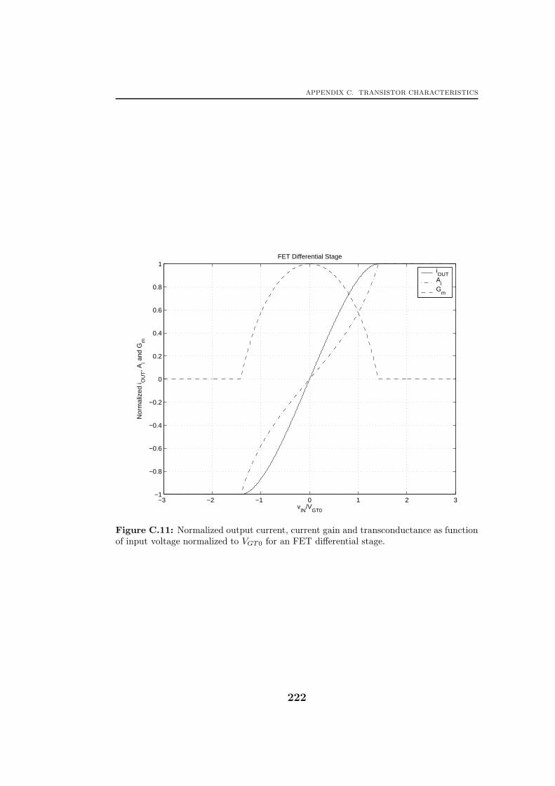
APPENDIX C. TRANSISTOR CHARACTERISTICS
−3 −2 −1 0 1 2 3−1
−0.8
−0.6
−0.4
−0.2
0
0.2
0.4
0.6
0.8
1FET Differential Stage
vIN
/VGT0
Nor
mal
ized
i OU
T, A
i and
Gm
iOUTA
iG
m
Figure C.11: Normalized output current, current gain and transconductance as functionof input voltage normalized to VGT0 for an FET differential stage.
222

C.5. FET DIFFERENTIAL STAGE
C.5.2 Small-Signal Characteristics
The small-signal transconductance defined as
Gm =∂iOUT∂vIN
(C.52)
is given by
Gm =
0 , vIN ≤ −√
2vGT0
−K(2v2GT0−v2IN )√4v2GT0−v2IN
,−√
2vGT0 > vIN >√
2vGT0
0 , vIN ≥√
2vGT0
(C.53)
or by
Gm =
0 , vIN ≤ −√
iSS
K
−K( iSSK
−v2IN)q2iSS
K−v2IN
,−√
iSS
K> vIN >
√iSS
K
0 , vIN ≥√
iSS
K
(C.54)
The small-signal current gain from the tail current source to the differen-tial output current, defined as
Ai =∂iOUT∂iSS
, (C.55)
is given by
Ai =
0 , vIN ≤ −√
2vGT0
− vIN
2√
4v2GT0−v2IN
,−√
2vGT0 > vIN >√
2vGT0
0 , vIN ≥√
2vGT0
(C.56)
or by
Ai =
0 , vIN ≤ −√
iSS
K
− vIN
2q
2iSSK
−v2IN
,−√
iSS
K> vIN >
√iSS
K
0 , vIN ≥√
iSS
K
(C.57)
Normalized plots of transconductance, Gm, and current gain, Ai, as func-tion of normalized input voltage, vIN , are shown in Figure C.11.
The small-signal transconductance from differential input voltage to dif-ferential output current using the small-signal parameters of transistors isgiven by
Gm = − gmAgmBgmA + gmB
. (C.58)
223

APPENDIX C. TRANSISTOR CHARACTERISTICS
Likewise, the small-signal current gain from tail current to differentialoutput current using the small-signal parameters of transistors is given by
Ai =1
2
gmA − gmBgmA + gmB
. (C.59)
C.5.3 Output Noise
The noise from the transistors is given by
i2dA = 4kBTγgmA (C.60)
andi2dB = 4kBTγgmB, (C.61)
respectively. Adding the noise contributions to the output current from thesetwo noise sources, we get the output current noise as
i2out = i2dA
(gmB
gmA + gmB
)2
+ i2dB
(gmA
gmA + gmB
)2
(C.62)
which can be rewritten as
i2out = 4kBTγgmAgmBgmA + gmB
= 4kBTγ|Gm|, (C.63)
where we have used (C.58).
C.5.4 Large-Signal Sinusoidal Operation
The describing function of an FET differential stage is shown in Figure C.12.We see that for an input-voltage amplitude Vin,1 & 2VGT0, where VGT0 is theoverdrive voltage of one transistor when conducting half the tail current, wemay approximate the describing function with
G1 ≈ − 2ISSπVin,1
, (C.64)
where ISS is the tail bias current.The two factors Kre and Kim, defined in Section 7.2.5 and related to the
noise conversion from the bias current source, iSS, to the output, are plottedin Figure C.13 as function of the input amplitude.
C.6 Contribution from Other Noise Sources
In this section we focus on the noise sources which are not considered above.We only deal with the small-signal case here.
224
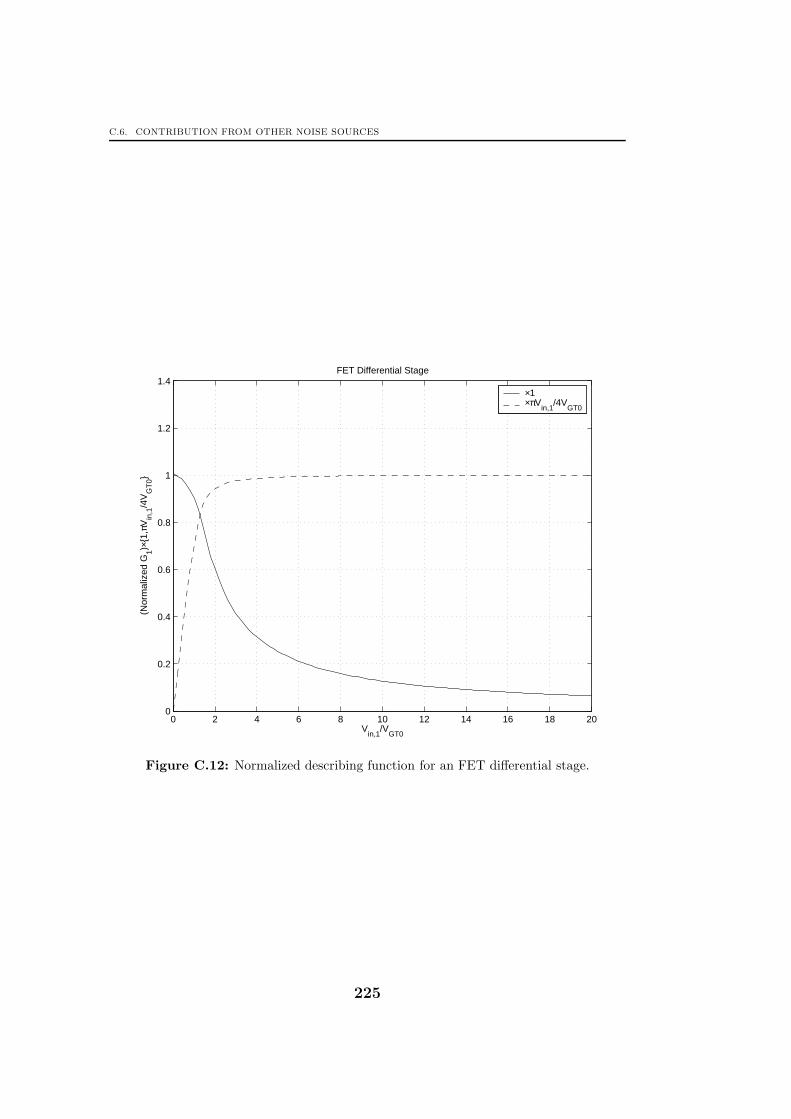
C.6. CONTRIBUTION FROM OTHER NOISE SOURCES
0 2 4 6 8 10 12 14 16 18 200
0.2
0.4
0.6
0.8
1
1.2
1.4FET Differential Stage
Vin,1
/VGT0
(Nor
mal
ized
G1)×
1,π
Vin
,1/4
VG
T0
×1×πV
in,1/4V
GT0
Figure C.12: Normalized describing function for an FET differential stage.
225
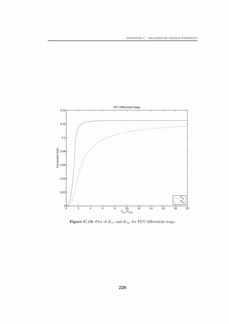
APPENDIX C. TRANSISTOR CHARACTERISTICS
0 2 4 6 8 10 12 14 16 18 200
0.02
0.04
0.06
0.08
0.1
0.12
0.14FET Differential Stage
Vin,1
/VGT0
Con
vers
ion
Gai
n
Kre
Kim
Figure C.13: Plot of Kre and Kim for FET differential stage.
226

C.6. CONTRIBUTION FROM OTHER NOISE SOURCES
C.6.1 Base–Emitter Resistance
We begin with the output impedance of the feedback network given by
Z22 =Z22
Z21Z21 ≈
Z21
Z11
1
gm, (C.65)
where we in the last approximation used that
Z21 =1
gm(C.66)
and assumed that Z11Z22 ≈ Z221, which is the case for low-phase-noise oscil-
lators. The base–emitter junction will contribute shot noise with a spectraldensity given by
i2b = 2kBTgmβ. (C.67)
Calculating the noise spectral density close to the fundamental frequency onthe collector terminal, we arrive at
i2c,b = i2bβ2
(Z22
Z22 + βgm
)2
≈ 2kBTgmβ
(Z21
Z11
1gm
Z21
Z11
1gm
+ βgm
)2
, (C.68)
where we in the last approximation have used (C.65). Rewriting this expres-sion once more, we get
i2c,b ≈ 2kBTgmβ
(Z21
Z11
Z21
Z11+ β
)2
≪ 2kBTgm = i2c , (C.69)
where we in the last comparison assume Z21
Z11≤ 1 and β ≫ 1.
C.6.2 Induced Gate Noise
In the FET we have induced gate noise coupling from the conducting channelto the gate terminal with a spectral density of
i2g = 4kBTδrgω2C2
GS, (C.70)
where δ ≈ 2γ and
rg =1
5gm. (C.71)
Combing these three expressions, we get
i2g =8kBTγ
5gmω2C2
GS, (C.72)
227

APPENDIX C. TRANSISTOR CHARACTERISTICS
which gives a noise spectral density around the fundamental frequency at thedrain terminal of
i2d,g = g2mZ
222
8kBTγ
5gmω2C2
GS ≈ 2
5
Z221
Z211
4kBTγgmω2C2
GS
g2m
=2
5
Z221
Z211
4kBTγgmω2
ω2T
≪ i2c ,
(C.73)where we in the last comparison assume Z21
Z11≤ 1 and ω
ωT≪ 1 where the
transit frequency, ωT , is defined as
ωT ≡ gmCGS
. (C.74)
228

Appendix DTwo-Port Parameters
I n this appendix, I give a short introduction to the modeling of passivetwo-port networks. In addition to the transfer functions, I also give thenoise of a general two-port network described by its Z-parameters.This appendix also contains a proof of a relationship for two-port networks
described by Z-parameters. It gives a lower bound on the product of inputresistance and output resistance in terms of the squared transfer resistance.
D.1 Two-Port Networks
Two-port networks have, as the name indicates, two ports as shown in Fig-ure D.1.
+
−V2
+
−V1
I1 I2
Z
Figure D.1: Two-port network.
The relations between the four signal quantities, I1, V1, I2 and V2 can bedescribed with four parameters. Depending on the use of the two-port, dif-ferent descriptions may be suitable. In Table D.1, four different descriptionsare given suited when the information signal is given as a current or voltage.There are more ways to describe a two-port network, for example chain-matrices which are useful when cascading several two-port networks. Theproperties of two-port networks are extensively covered in literature aboutnetwork analysis and synthesis.
229

APPENDIX D. TWO-PORT PARAMETERS
Table D.1: Types of two-ports.
Input Output Parameters
Voltage Voltage GVoltage Current YCurrent Voltage ZCurrent Current H
D.2 Z-Parameters
Z-parameters are best suited to model a two-port networks when the inputsignal is a current, I1, and the output signal is a voltage, V2. For a generaltwo-port network, we have the relationships
[V1
V2
]=
[Z11 Z12
Z21 Z22
] [I1I2
](D.1)
between the currents and voltages of the two ports. If the two-port networkis reciprocal we also have that Z12 = Z21.
The noise of a two-port network may be modeled by two noise sources,voltages and/or currents, with cross-correlation [Rothe and Dahlke, 1956,Bennett, 1960]. In the special case when the two-port network is passiveand is not impedance loaded, the output noise voltage spectral density of thetwo-port network is simply
v22 = 4kBTℜ[Z22], (D.2)
assuming that all components in the two-port network have the same tem-perature, T . However, this result does not necessarily hold for time-varyingnetworks [Coram et al., 2000].
D.3 Impedance Parameter Inequality
We assume that the two-port network is passive and hence reciprocal withZ12 = Z21. Since we assume that the two-port network is passive, we musthave an input impedance with positive real part for each port. We alsoassume that all Z-parameters are real.
Setting I2 = 0, we haveZ11 ≥ 0 (D.3)
and setting I1 = 0, we haveZ22 ≥ 0. (D.4)
230

D.3. IMPEDANCE PARAMETER INEQUALITY
Setting V1 = 0, we have
Z22 −Z12Z21
Z11≥ 0. (D.5)
Combining (D.3), (D.4) and (D.5), we get
Z11Z22 ≥ Z221. (D.6)
The equality is fulfilled for example for a one-port network, which may bemodeled by a two-port network with input and output ports connected to-gether. In this case we have that Z11 = Z12 = Z21 = Z22.
231

APPENDIX D. TWO-PORT PARAMETERS
232

Appendix EDefinition of Q-value
I n this appendix, we treat a few matters related to the definition of Q-value used in this thesis. In addition to a discussion of the connectionbetween the Q-value and indirect frequency stability, we show that the
definition gives us a positive Q-value.We choose to define the Q-value for an oscillator as
Q ≡ −ω0
2
(∂α
∂ω+∂ζ
∂ω
). (E.1)
The indirect frequency stability, SF , is defined as
SF ≡ ω0
(∂α
∂ω+∂ζ
∂ω
)= −2Q (E.2)
and is a measure of the frequency sensitivity against change in the loop phase,α + ζ .
E.1 Sign of Q-value
In this section, we show that the definition of Q above gives a positive valuefor stable limit cycles.
To make this derivation simple, we assume that the feedback networkdetermines the frequency and does not depend on the amplitude, accordingto
H1(ω) = A(ω)ejα(ω). (E.3)
We also assume that the active part determines the amplitude and does notdepend on the frequency and is given by
F1(X1) = B(X1), (E.4)
233

APPENDIX E. DEFINITION OF Q-VALUE
where X1 is the amplitude of the input signal to the active part at thefundamental frequency. This last assumption simplifies the Q-value to
Q = −ω0
2
∂α
∂ω. (E.5)
For a limit cycle, the Barkhausen criterion given as
H1(ω)F1(X1) = 1 (E.6)
is fulfilled.Considering only the fundamental tone, we have the limit cycle signal as
ℜ[X1ejω0t]. Consider now a perturbation that changes the amplitude from
X1 to X1 + X∆,1 and the complex frequency from ω0 to ω0 + ω∆ + jσ∆. Ifthe oscillator is to return to its limit cycle, σ∆ must be positive for the newfactor e−σ∆ to converge to unity.
We rewrite the Barkhausen criterion as
Aejα(ω)B1(X1) = 1. (E.7)
If we Taylor expand this expression and keep only the first term, we get
(ω∆ + jσ∆)
(B1(ω)
∂A1(ω)
∂ω+ j
∂α(ω)
∂ω
)+X∆,1A(ω)
∂B1(X1)
∂X1
= 0. (E.8)
This expression can be split into its real part, given by
ω∆B1(ω)∂A1(ω)
∂ω− σ∆
∂α(ω)
∂ω+X∆,1A(ω)
∂B1(X1)
∂X1
= 0, (E.9)
and its imaginary part, given by
ω∆∂α(ω)
∂ω+ σ∆B1(ω)
∂A1(ω)
∂ω= 0. (E.10)
Eliminating ω∆ from these two equations, we get
X∆,1A(ω)∂B1(X1)
∂X1
∂α(ω)
∂ω= σ∆
((∂α(ω)
∂ω
)2
+
(B1(ω)
∂A1(ω)
∂ω
)2).
(E.11)Since we want σ∆ to be positive for a positive amplitude step X∆,1, the
following inequality must hold:
A(ω)∂B1(X1)
∂X1
∂α(ω)
∂ω> 0. (E.12)
234

E.1. SIGN OF Q-VALUE
We finally assume that the absolute value of the describing functionF1(X1) = B(X1) is a monotonously decreasing function of the amplitudeX1 around the limit cycle and thereby get
∂α(ω)
∂ω< 0, (E.13)
which in turn gives a positive value for the quality factor Q when inserted in(E.5).
235

APPENDIX E. DEFINITION OF Q-VALUE
236
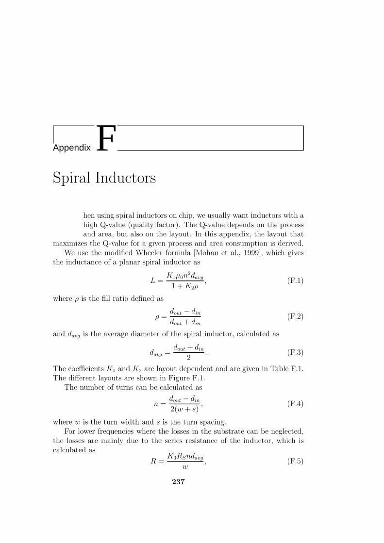
Appendix FSpiral Inductors
W hen using spiral inductors on chip, we usually want inductors with ahigh Q-value (quality factor). The Q-value depends on the processand area, but also on the layout. In this appendix, the layout that
maximizes the Q-value for a given process and area consumption is derived.We use the modified Wheeler formula [Mohan et al., 1999], which gives
the inductance of a planar spiral inductor as
L =K1µ0n
2davg1 +K2ρ
, (F.1)
where ρ is the fill ratio defined as
ρ =dout − dindout + din
(F.2)
and davg is the average diameter of the spiral inductor, calculated as
davg =dout + din
2. (F.3)
The coefficients K1 and K2 are layout dependent and are given in Table F.1.The different layouts are shown in Figure F.1.
The number of turns can be calculated as
n =dout − din2(w + s)
, (F.4)
where w is the turn width and s is the turn spacing.For lower frequencies where the losses in the substrate can be neglected,
the losses are mainly due to the series resistance of the inductor, which iscalculated as
R =K3RSndavg
w, (F.5)
237

APPENDIX F. SPIRAL INDUCTORS
Table F.1: Coefficients for inductance, resistance and Q-value expressions.
Layout K1 K2 K3 K4 K5 ξopt
Square 2.34 2.75 4.00 0.0828 0.0828 0.248Hexagonal 2.33 3.82 3.46 0.0771 0.0828 0.323Octagonal 2.25 3.55 3.31 0.0816 0.0897 0.307
doutdin
s
dout
s
doutdin
swww
din
Square Hexagonal Octagonal
Figure F.1: Spiral inductor geometries.
where RS is the sheet resistance of the conductor (including possible skineffect) and K3 is a coefficient which gives the length of one turn when multi-plied with the diameter of that turn (and would be equal to π for a circularinductor). Values for the coefficient K3 are given in Table F.1 for the differentlayouts.
The Q-value of an inductor is by definition
Q ≡ ωL
R=
ωK1µ0doutw
2K3RS(w + s)
1 − ξ2
1 +K2 + ξ(1 −K2), (F.6)
where we define the ratio between inner and outer diameter as
ξ =dindout
. (F.7)
We calculate the ξ that gives maximum Q-value by taking the derivativeof the second fraction and equating to zero. We get the following optimumratio:
ξopt =
√K2 − 1√K2 + 1
(F.8)
with the following expression for Q-value when ξ = ξopt:
Qopt =ωK4µ0doutw
RS(w + s), (F.9)
238

where
K4 =K1
2K3
1 − ξ2opt
1 +K2 + ξopt(1 −K2). (F.10)
Values for the optimum ratio ξopt and the coefficient K4 are given in Table F.1.The different layouts have different area, A, for the same outer diameter,
dout, which makes comparisons based on the expression above misleading.Rewriting (F.9), we get
Qopt =ωK5µ0
√Aw
RS(w + s), (F.11)
where K5 is a coefficient with the values given in Table F.1 for differentlayouts. As seen from the values in Table F.1, the three different layoutsgive approximately the same Q-value. We also see that the Q-value is notstrongly dependent on ξ close to the optimum at ξ = ξopt in Figure F.2.
0 0.1 0.2 0.3 0.4 0.5 0.6 0.7 0.8 0.9 10
0.01
0.02
0.03
0.04
0.05
0.06
0.07
0.08
0.09
ξ=din
/dout
K5(ξ
)
SquareHexagonalOctagonal
Figure F.2: Plot of coefficient K5 as function of the ratio ξ = din/dout for three differentinductor layouts.
The layouts of inductors used in the calculations of this appendix are notthe optimal ones and better performance can be achieved if one do not usefixed conductor widths and spacings. If the substrate losses are not negligible,
239

APPENDIX F. SPIRAL INDUCTORS
special arrangements such as shielding may reduce these losses and increasethe Q-value.
240
Bibliography
[Adler, 1946] Adler, R. (1946). A study of locking phenomena in oscillators.Proceedings of the IRE and Waves and Electrons, 34(6):351–357.
[Andreani and Mattisson, 2000] Andreani, P. and Mattisson, S. (2000). Onthe use of mos varactors in RF VCO’s. IEEE Journal of Solid-State Cir-cuits, 35(6):905–910.
[Andreani and Sjoland, 2002] Andreani, P. and Sjoland, H. (2002). Tail cur-rent noise suppression in RF CMOS VCOs. IEEE Journal of Solid-StateCircuits, 37(3):342–348.
[Andreani et al., 2005] Andreani, P., Wang, X., Vandi, L., and Fard, A.(2005). A study of phase noise in colpitts and LC-tank CMOS oscilla-tors. IEEE Journal of Solid-State Circuits, 40(5):1107–1118.
[Aparicio and Hajimiri, 2002] Aparicio, R. and Hajimiri, A. (2002). A noise-shifting differential colpitts VCO. IEEE Journal of Solid-State Circuits,37(12):1728–1736.
[Atherton, 1975] Atherton, D. P. (1975). Nonlinear Control Engineering.Van Nostrand Reinhold Company.
[Atherton and Dorrah, 1980] Atherton, D. P. and Dorrah, H. T. (1980).A survey on non-linear oscillations. International Journal of Control,31(6):1041–1105.
[Bennett, 1960] Bennett, W. R. (1960). Electrical Noise. McGraw-Hill.
[Berny et al., 2005] Berny, A. D., Niknejad, A. M., and Meyer, R. G. (2005).A 1.8-GHz LC VCO with 1.3-GHz tuning range and digital amplitudecalibration. IEEE Journal of Solid-State Circuits, 40(4):909–917.
241

BIBLIOGRAPHY
[Bloom and Nemirovsky, 1991] Bloom, I. and Nemirovsky, Y. (1991). 1/fnoise reduction of metal-oxide-semiconductor transistors by cycling frominversion to accumulation. Applied Physics Letters, 58(15):1664–1666.
[Bunch and Raman, 2003] Bunch, R. L. and Raman, S. (2003). Large-signalanalysis of MOS varactors in CMOS −Gm LC VCOs. IEEE Journal ofSolid-State Circuits, 38(8):1325–1332.
[Cherry and Hooper, 1968] Cherry, E. M. and Hooper, D. E. (1968). Ampli-fying Devices and Low-Pass Amplifier Design. John Wiley and Sons.
[Clarke and Hess, 1971] Clarke, K. K. and Hess, D. T. (1971). Communica-tion Circuits: Analysis and Design. Addison-Wesley Publishing Company.
[Coram et al., 2000] Coram, G. J., Anderson, B. D. O., and Wyatt, Jr., J. L.(2000). Limits to the fluctuation-dissipation theorem for nonlinear circuits.IEEE Transactions on Circuits and Systems–I: Fundamental Theory andApplications, 47(9):1323–1329.
[Darabi and Abidi, 2000] Darabi, H. and Abidi, A. A. (2000). A 4.5-mw900-MHz CMOS receiver for wireless paging. IEEE Journal of Solid-StateCircuits, 35(8):1085–1096.
[Dec and Suyama, 2000] Dec, A. and Suyama, K. (2000). A 1.9-GHz CMOSVCO with micromachined electromechanically tunable capacitors. IEEEJournal of Solid-State Circuits, 35(8):1231–1237.
[Demir, 1998] Demir, A. (1998). Phase noise in oscillators: DAEs and col-ored noise sources. In IEEE/ACM International Conference on Computer-Aided Design, pages 170–177.
[Demir et al., 2000] Demir, A., Mehrotra, A., and Roychowdhury, J. (2000).Phase noise in oscillators: A unifying theory and numerical methods forcharacterization. IEEE Transactions on Circuits and Systems–I: Funda-mental Theory and Applications, 47(5):655–674.
[Dierickx and Simoen, 1992] Dierickx, B. and Simoen, E. (1992). The de-crease of “random telegraph signal” noise in metal-oxide-semiconductorfield-effect transistors when cycled from inversion to accumulation. Jour-nal of Applied Physics, 71(4):2028–2029.
[Falk and Schwarz, 2000] Falk, T. and Schwarz, W. (2000). Impulse sensitiv-ity functions of oscillators. In IEEE International Symposium on Circuitsand Systems (ISCAS), pages I–647–650.
242

BIBLIOGRAPHY
[Falk and Schwarz, 2003] Falk, T. and Schwarz, W. (2003). An explicit for-mulation of the sensitivity function of two-dimensional oscillators. In Inter-national IEEE Workshop on Nonlinear Dynamics of Electronic Systems,pages 81–84.
[Fong et al., 2004] Fong, N., Kim, J., Plouchart, J.-O., Zamdmer, N., Liu,D., Wagner, L., Plett, C., and Tarr, G. (2004). A low-voltage 40-GHz com-plementary VCO with 15% frequency tuning range in SOI CMOS technol-ogy. IEEE Journal of Solid-State Circuits, 39(5):841–846.
[Fong et al., 2003] Fong, N. H. W., Plouchart, J.-O., Zamdmer, N., Liu, D.,Wagner, L. F., Plett, C., and Tarr, N. G. (2003). Design of wide-bandCMOS VCO for multiband wireless LAN applications. IEEE Journal ofSolid-State Circuits, 38(8):1333–1342.
[Freidlin and Wentzell, 1998] Freidlin, M. I. and Wentzell, A. D. (1998).Random Perturbations of Dynamical Systems. Springer-Verlag, second edi-tion.
[Gelb and Velde, 1968] Gelb, A. and Velde, W. E. V. (1968). Multiple-inputDescribing Functions and Nonlinear System Design. McGraw-Hill.
[Getreu, 1976] Getreu, I. (1976). Modeling the Bipolar Transistor. Tektronix.
[Ghanta et al., 2004] Ghanta, P., Li, Z., and Roychowdhury, J. (2004). Ana-lytical expressions for phase noise eigenfunctions of LC oscillators. In IEEEAsia and South Pacific Design Automation Conference, pages 175–180.
[Groszkowski, 1964] Groszkowski, J. (1964). Frequency of Self-Oscillations.PWN – Polish Scientific Publishers.
[Gustafsson et al., 1972] Gustafsson, L., Hansson, G. H. B., and Lundstrom,K. I. (1972). On the use of describing functions in the study of nonlinearactive microwave circuits. IEEE Transactions on Microwave Theory andTechniques, 20(6):402–409.
[Hajimiri and Lee, 1998] Hajimiri, A. and Lee, T. H. (1998). A general the-ory of phase noise in electrical oscillators. IEEE Journal of Solid-StateCircuits, 33(2):179–194.
[Ham and Hajimiri, 2001] Ham, D. and Hajimiri, A. (2001). Concepts andmethods in optimization of integrated LC VCOs. IEEE Journal of Solid-State Circuits, 36(6):896–909.
243

BIBLIOGRAPHY
[Hegazi and Abidi, 2003] Hegazi, E. and Abidi, A. A. (2003). Varactor char-acteristics, oscillator tuning curves, and AM–FM conversion. IEEE Jour-nal of Solid-State Circuits, 38(6):1033–1039.
[Hegazi et al., 2005] Hegazi, E., Rael, J., and Abidi, A. (2005). The De-signer’s Guide to High-Purity Oscillators. Kluwer Academic Publishers.
[Hegazi et al., 2001] Hegazi, E., Sjoland, H., and Abidi, A. A. (2001). Afiltering technique to lower LC oscillator phase noise. IEEE Journal ofSolid-State Circuits, 36(12):1921–1930.
[Huang, 1998] Huang, Q. (1998). On the exact design of RF oscillators. InIEEE Custom Integrated Circuits Conference, pages 41–44.
[Hung and O, 2000] Hung, C. M. and O, K. K. (2000). A packaged 1.1-GHzCMOS VCO with phase noise of -126 dBc/Hz at a 600-khz offset. IEEEJournal of Solid-State Circuits, 35(1):100–103.
[Jerng and Sodini, 2005] Jerng, A. and Sodini, C. G. (2005). The impactof device type and sizing on phase noise mechanisms. IEEE Journal ofSolid-State Circuits, 40(2):360–368.
[Jezewski, 1974] Jezewski, M. T. (1974). An approach to the analysis ofinjection-locked oscillators. IEEE Transactions on Circuits and Systems,21(3):395–401.
[Jia et al., 2004] Jia, L., Ma, J.-G., Yeo, K. S., and Do, M. A. (2004). 9.3–10.4-GHz-band cross-coupled complementary oscillator with low phase-noise performance. IEEE Transactions on Microwave Theory and Tech-niques, 52(4):1273–1278.
[Kaertner, 1990] Kaertner, F. X. (1990). Analysis of white and f−α noisein oscillators. International Journal of Circuit Theory and Applications,18:485–519.
[Kao and Hsu, 2005] Kao, Y.-H. and Hsu, M.-T. (2005). Theoretical analysisof low phase noise design of CMOS VCO. IEEE Microwave and WirelessComponents Letters, 15(1):33–35.
[Klimovitch, 2000] Klimovitch, G. V. (2000). Near-carrier oscillator spec-trum due to flicker and white noise. In IEEE International Symposium onCircuits and Systems (ISCAS), pages I–703–706.
[Kundert, 2000] Kundert, K. (2000). A formal top-down design process formixed-signal circuits. In Advances in Analog Circuit Design.
244

BIBLIOGRAPHY
[Kundert, 1999] Kundert, K. S. (1999). Introduction to RF simulation andits application. IEEE Journal of Solid-State Circuits, 34(9):1298–1319.
[Kurokawa, 1973] Kurokawa, K. (1973). Injection locking of microwave solid-state oscillators. Proceedings of the IEEE, 61(10):1386–1410.
[Leeson, 1966] Leeson, D. B. (1966). A simple model of feedback oscillatornoise spectrum. Proceedings of the IEEE, 54(2):329–330.
[Levantino et al., 2004] Levantino, S., Bonfanti, A., Romano, L., Samori,C., and Lacaita, A. L. (2004). Differential tuning oscillators with reducedflicker noise upconversion. In IEEE International Conference on Electron-ics, Circuits and Systems, pages 33–36.
[Levantino et al., 2002] Levantino, S., Samori, C., Bonfanti, A., Gierkink, S.L. J., Lacaita, A. L., and Boccuzzi, V. (2002). Frequency dependence onbias current in 5-GHz CMOS VCOs: Impact on tuning range and flickernoise upconversion. IEEE Journal of Solid-State Circuits, 37(8):1003–1011.
[Mehrotra and Sangiovanni-Vincentelli, 1999] Mehrotra, A. andSangiovanni-Vincentelli, A. L. (1999). Noise analysis of non-autonomousradio frequency circuits. In IEEE/ACM International Conference onComputer-Aided Design, pages 55–60.
[Mohan et al., 1999] Mohan, S. S., del Mar Hershenson, M., Boyd, S. P.,and Lee, T. H. (1999). Simple accurate expressions for planar spiral in-ductances. IEEE Journal of Solid-State Circuits, 34(10):1419–1424.
[Moon et al., 2004] Moon, H., Kang, S., Kim, Y. T., and Lee, K. (2004). Afully differential LC-VCO using a new varactor control structure. IEEEMicrowave and Wireless Components Letters, 14(9):410–412.
[Nguyen and Meyer, 1992] Nguyen, N. M. and Meyer, R. G. (1992). Start-up and frequency stability in high-frequency oscillators. IEEE Journal ofSolid-State Circuits, 27(5):810–820.
[O, 1998] O, K. (1998). Estimation methods for quality factors of inductorsfabricated in silicon integrated circuit process technologies. IEEE Journalof Solid-State Circuits, 33(8):1249–1252.
[Parzen, 1983] Parzen, B. (1983). Design of Crystal and Other HarmonicOscillators. John Wiley & Sons.
245

BIBLIOGRAPHY
[Pettai, 1984] Pettai, R. (1984). Noise in Receiving Systems. John Wiley &Sons.
[Rael and Abidi, 2000] Rael, J. J. and Abidi, A. A. (2000). Physical pro-cesses of phase noise in differential LC oscillators. In IEEE Custom Inte-grated Circuits Conference, pages 569–572.
[Rogers et al., 2000] Rogers, J. W. M., Macedo, J. A., and Plett, C. (2000).The effect of varactor nonlinearity on the phase noise of completely inte-grated VCOs. IEEE Journal of Solid-State Circuits, 35(9):1360–1367.
[Rothe and Dahlke, 1956] Rothe, H. and Dahlke, W. (1956). Theory of noisyfourpoles. Proceedings of the IRE, 44(6):811–818.
[Samori et al., 1998] Samori, C., Lacaita, A. L., Villa, F., and Zappa, F.(1998). Spectrum folding and phase noise in LC tuned oscillators. IEEETransactions on Circuits and Systems–II: Analog and Digital Signal Pro-cessing, 45(7):781–790.
[Samori et al., 2000] Samori, C., Lacaita, A. L., Zanchi, A., Levantino, S.,and Calı, G. (2000). Phase noise degradation at high oscillation amplitudesin LC-tuned VCO’s. IEEE Journal of Solid-State Circuits, 35(1):96–99.
[Stover, 1966] Stover, H. L. (1966). Theoretical explanation for the outputspectra of unlocked driven oscillators. Proceedings of the IEEE, 54(2):310–311.
[Svelto et al., 2000] Svelto, F., Deantino, S., and Castello, R. (2000). A 1.3GHz low-phase noise fully tunable CMOS LC VCO. IEEE Journal ofSolid-State Circuits, 35(3):356–361.
[Tsividis, 1999] Tsividis, Y. (1999). The MOS Transistor. McGraw-Hill,second edition.
[Unkrich and Meyer, 1982] Unkrich, M. A. and Meyer, R. G. (1982). Con-ditions for start-up in crystal oscillators. IEEE Journal of Solid-StateCircuits, 17(1):87–90.
[van der Pol, 1934] van der Pol, B. (1934). The nonlinear theory of electricoscillations. Proceedings of the IRE, 22(9):1051–1086.
[van der Tang and Kasperkovitz, 2000] van der Tang, J. and Kasperkovitz,D. (2000). Oscillator design efficiency: A new figure of merit for oscillatorbenchmarking. In IEEE International Symposium on Circuits and Systems(ISCAS), pages II–533–536.
246

BIBLIOGRAPHY
[van der Tang et al., 2003] van der Tang, J., Kasperkovitz, D., and vanRoermund, A. (2003). High-Frequency Oscillator Design for IntegratedTransceivers. Kluwer Academic Publishers.
[van Staveren et al., 2001] van Staveren, A., Verhoeven, C. J. M., andvan Roermund, A. H. M. (2001). Structured Electronic Design: High-Performance Harmonic Oscillators and Bandgap References. Kluwer Aca-demic Publishers.
[Vanassche et al., 2002] Vanassche, P., Gielen, G., and Sansen, W. (2002).On the difference between two widely publicized methods for analyzingoscillator phase behavior. In IEEE/ACM International Conference onComputer-Aided Design, pages 229–233.
[Vanassche et al., 2003] Vanassche, P., Gielen, G., and Sansen, W. (2003).A generalized method for computing oscillator phase noise spectra. InIEEE/ACM International Conference on Computer-Aided Design, pages247–250.
[Vanassche et al., 2004] Vanassche, P., Gielen, G., and Sansen, W. (2004).Efficient analysis of slow-varying oscillator dynamics. IEEE Transactionson Circuits and Systems–I: Regular Papers, 51(8):1457–1467.
[Verhoeven et al., 2003] Verhoeven, C. J. M., van Staveren, A., Monna, G.L. E., Kouwenhoven, M. H. L., and Yildiz, E. (2003). Structured ElectronicDesign: Negative-Feedback Amplifiers. Kluwer Academic Publishers.
[Vittoz et al., 1988] Vittoz, E. A., Degrauwe, M. G. R., and Bitz, S. (1988).High-performance crystal oscillator circuits: Theory and application.IEEE Journal of Solid-State Circuits, 23(3):774–783.
[Westra et al., 1999] Westra, J. R., Verhoeven, C. J. M., and van Roermund,A. H. M. (1999). Oscillators and Oscillator Systems: Classification, Anal-ysis and Synthesis. Kluwer Academic Publishers.
[Yoon et al., 2005] Yoon, S.-W., Pinel, S., and Laskar, J. (2005). A 0.35-µmCMOS 2-GHz VCO in wafer-level package. IEEE Microwave and WirelessComponents Letters, 15(4):229–231.
[Zanchi et al., 2001] Zanchi, A., Samori, C., Levantino, S., and Lacaita, A. L.(2001). A 2-V 2.5-GHz -104-dBc/Hz at 100 kHz fully integrated VCO withwide-band low-noise automatic amplitude control loop. IEEE Journal ofSolid-State Circuits, 36(4):611–619.
247

BIBLIOGRAPHY
[Zhang et al., 2004] Zhang, H., Zhang, J., Zhou, D., Liu, J., Jiang, L., andPan, Y. (2004). A closed-form phase noise solution for an ideal LC oscilla-tor. In IEEE International Symposium on Circuits and Systems (ISCAS),pages IV–768–771.
248

Index
Active network, 54–63AM-to-PM conversion, 12
in simulated topology, 155–157AM-to-PM conversion factor
definition, 132Amplitude control, 79–87
using automatic amplitude con-trol, 83–86
using diode, 81–82using nonlinearity in the active com-
ponent, 82–83using temperature-sensitive resis-
tor, 80–81Amplitude detector, 85–86Amplitude noise, 10–11Automatic amplitude control, 150–151Average amplitude detector, 85
Base resistance, 153–154Bias current source, 63–66Biasing, 56–62
of differential pair, 59–60of one transistor, 57–59
Bipolar junction transistor, 183–185BJT differential stage, 187–192
Capacitors, 43–44Common-mode oscillations, 60–61Component Sizing, 19–21Correction to oscillation frequency, 142–
144
Crystal networks, 53–54Crystal Oscillator, 21–27Crystals, 44–46
Describing functions, 165–175for arc-tan nonlinearity, 171–172for clipping nonlinearity, 173for exponential nonlinearity, 174–
175for impulse nonlinearity, 175for limiter nonlinearity, 174for polynomial nonlinearity, 170for tanhyp nonlinearity, 172–173how to calculate, 165–167
Design methodology, 15–42Diode, 181–183Diode limiting, 149–150Diode varactor, 94–99
in simulated topology, 155–157
Feedback network, 43–54transfer function, 84
FET differential stage, 192–195Field-effect transistor, 186–187Frequency tuning, 54, 89–101
Impulse sensitivity functions, 121–137definition of, 122for disturbances, 132–137for linear feedback network, 124–
126for the general case, 127–132
249

INDEX
how to derive, 122–124In-phase incremental describing func-
tions, 168Incremental describing functions, 167–
170Indirect frequency stability, 203Inductors, 44Injection locking, 12, 118–120
JFET VCO, 27–34
Large-signal capacitance, 90–91of diode varactor, 97of MOS varactor, 100
LC networks, 49–52
MOS varactor, 99–101MOSFET VCO, 34–41
Noise factor, 113
Optimization, 21Oscillator
analysis of, 2–3design of, 3, 13feedback model of, 7–8operation of, 5–7specification of, 12–13
Oscillator design efficiency, 157–160definition, 17of different bias arrangements, 66–
78
Parallel connected reactances, 52Peak detector, 85–86Phase noise, 11–12, 103–120
definition, 11due to 1/f noise, 114–117due to disturbances, 117due to frequency tuning, 92–94due to white noise, 104–114from active network, 105–106, 114–
115
from biasing network, 108–112, 116from diode limiting, 107–108from feedback network, 104–105,
114from series base and gate resis-
tances, 106–107Phase noise due to 1/f noise
in simulated topology, 157Phase-noise spectrum, 11, 177–180Piezoelectric resonators, 44–46Power efficiency
definition, 18of one-transistor networks, 55of two-transistor networks, 55–56
Q-valueof capacitor, 44of crystal network, 53–54of inductor, 44of LC network, 49of oscillator, 203–204
definition, 203of transimpedance network, 48
Quadrature-phase incremental describ-ing functions, 169–170
Series connected reactances, 52Simulation, 21Specification, 16–18Spiral inductors, 205–207Squegging, 61–62Start-up, 62–63
Topology selection, 18–19Two-port parameters, 199–201
VCO tuning constant, 91–92
Z-parameters, 200–201of transimpedance network, 47–
48
250