Embed Size (px)
Citation preview

A Facile Route for Producing Single-Crystalline Epitaxial PerovskiteOxide Thin FilmsAndrew R. Akbashev, Guannan Chen, and Jonathan E. Spanier*
Department of Materials Science and Engineering, Drexel University, Philadelphia, Pennsylvania 19104, United States
*S Supporting Information
ABSTRACT: We report how a low vacuum pressure process followed by a few-minute annealing enables epitaxial stabilization,producing high-quality, phase-pure, single-crystalline epitaxial, and misfit dislocation-free BiFeO3(001) thin films on SrTiO3(001)at ∼450 °C less than current routes. These results unambiguously challenge the widely held notion that atomic layer deposition(ALD) is not appropriate for attaining high-quality chemically complex oxide films on perovskite substrates in single-crystallineepitaxial form, demonstrating applicability as an inexpensive, facile, and highly scalable route.
KEYWORDS: atomic layer deposition, BiFeO3, perovskite, ferroelectric, multiferroic, epitaxy
The design of modern electronic and spintronic devicesrequires materials with unique properties such as high
tunneling magnetoresistance and spin filtering efficiency, high-κdielectricity, strong magnetic anisotropy, multiferroicity, andsuperconductivity.1−3 These properties in turn require high-vacuum and high-temperature thin-film deposition methodsthat can produce these materials with exceptional crystallinequality.4−6 However, realization of industrially scalable devicetechnologies relies on atomically controlled thin filmpreparation routes in which heteroepitaxial thin films ofcomparably high quality can be attained, but at considerablylower temperature and pressure, and cost.Atomic layer deposition (ALD) has become one of the most
versatile and widely implemented techniques for obtainingatomically smooth conformal thin films of inorganic andorganic materials in an energy-efficient and environmentallyfriendly manner.7−10 ALD is advantageous in achievingconformal coating of high-aspect-ratio structures and alsoallows for a very easy atomic control of the thickness over largeareas without high vacuum. While ALD of technologicallyimportant binary oxides is prevalent,7−10 including high-κ gateinsulators, there are far fewer reports of ALD of complexperovskite oxides, which are polycrystalline and/or possessmisfit dislocations if epitaxial.11−15 This scarcity is owing todifficulties particularly in the growth optimization and anappropriate choice of the precursors with similar ALD
temperature windows, high vapor pressure, and the presenceof distinct catalytic processes on differently terminated surfacesduring deposition. In principle, there are no limitations to thesingle-crystalline epitaxial phase formation via ALD, and ALDcan be considered as a potential route for obtaining single-crystalline epitaxial films of perovskite oxides on perovskitesubstrates equal in quality to those obtained using high-temperature chemical or physical vapor deposition approaches.Growth of a technologically important multifunctional material,BiFeO3 via ALD is chosen to demonstrate the feasibility of thisconcept.BiFeO3 is one of the most technologically promising
multiferroics.16 It is also attractive among ferroelectric materialsfor solar energy conversion due to its large photovoltage andvisible photon energy bandgap (∼2.7 eV). While high-qualityheteroepitaxial BiFeO3 thin films have been obtained throughhigh-vacuum physical vapor deposition4,17 and molecular beamepitaxy (MBE),18 and metal−organic chemical vapor deposi-tion (MOCVD),19,20 an inexpensive low-vacuum surfacereaction rate-limited deposition route for obtaining thistechnologically promising perovskite oxide (or any perovskiteoxide) in single-crystalline high-quality heteroepitaxial form hasbeen elusive. BiFeO3 is considered difficult to grow in thin-film
Received: August 10, 2013
Letter
pubs.acs.org/NanoLett
© XXXX American Chemical Society A dx.doi.org/10.1021/nl4030038 | Nano Lett. XXXX, XXX, XXX−XXX
form due to Bi2O3 volatilization during deposition, which leadsto the appearance of parasitic phases in large quantities.21
Heteroepitaxial BiFeO3 via ALD requires an appropriatechoice of precursors that (1) can adsorb on the surface and beoxidized to enable production of a ternary oxide in sequentialcycles, (2) does not introduce other cations/anions (con-tamination) into the films, and (3) have overlapping ALDtemperature windows. From a small number of known bismuthprecursors we chose Bi(mmp)3 (tris(1-methoxy-2-methyl-2-propoxy)bismuth) as it has a wide ALD temperature window(at least 200−300 °C),22 high stability, and contains only Biand organic ligands. Bi(mmp)3 was reported to have a firstconsiderable weight loss in the temperature range of ∼130−170°C due to the volatilization of the compound and the second
weight loss after 170 °C attributed to the decomposition ofBi(mmp)3.
23 We chose 135−145 °C as an evaporationtemperature of Bi(mmp)3, which provided sufficientlyreproducible precursor pulses. We also selected Fe(C5H5)2(ferrocene) since it has an excellent thermal stability, smallmolecule size, and can easily be oxidized by ozone. We find thebest evaporation temperature for the ferrocene source to be 90°C. In our preliminary ALD experiments, use of ferrocene ledto a slow but very stable growth of iron oxide for substratetemperatures in the range of 150−300 °C when ozone (<10 %)was used as an oxidizing agent. To obtain a preliminary Bi−Fe−O film the substrate was heated to 250 °C and bothprecursors were sequentially delivered into the ALD reactor, asschematically illustrated in Figure 1. The number of pulses for
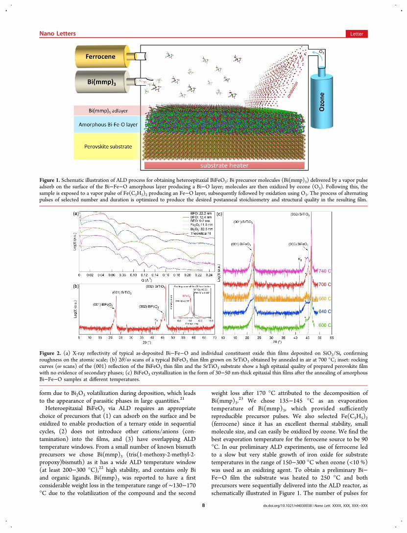
Figure 1. Schematic illustration of ALD process for obtaining heteroepitaxial BiFeO3: Bi precursor molecules (Bi(mmp)3) delivered by a vapor pulseadsorb on the surface of the Bi−Fe−O amorphous layer producing a Bi−O layer; molecules are then oxidized by ozone (O3). Following this, thesample is exposed to a vapor pulse of Fe(C5H5)2 producing an Fe−O layer, subsequently followed by oxidation using O3. The process of alternatingpulses of selected number and duration is optimized to produce the desired postanneal stoichiometry and structural quality in the resulting film.
Figure 2. (a) X-ray reflectivity of typical as-deposited Bi−Fe−O and individual constituent oxide thin films deposited on SiO2/Si, confirmingroughness on the atomic scale; (b) 2θ/ω scans of a typical BiFeO3 thin film grown on SrTiO3 obtained by annealed in air at 700 °C; inset: rockingcurves (ω scans) of the (001) reflection of the BiFeO3 thin film and the SrTiO3 substrate show a high epitaxial quality of prepared perovskite filmwith no evidence of secondary phases; (c) BiFeO3 crystallization in the form of 30−50 nm-thick epitaxial thin films after the annealing of amorphousBi−Fe−O samples at different temperatures.
Nano Letters Letter
dx.doi.org/10.1021/nl4030038 | Nano Lett. XXXX, XXX, XXX−XXXB

each precursor within each subcycle was minimized whilemaintaining the correct stoichiometry in the final Bi−Fe−Ofilms. As expected, Bi(mmp)3 showed a higher growth rate thanFe(C5H5)2, thus the ratio between the number of pulses wasNFe:NBi ≈ 3−5. Each Bi−Fe−O thin film deposition run wascarried out on both SiO2/Si and SrTiO3(001) simultaneously.Usually in ALD-limited growth the thickness of a simple oxidefilm depends nonlinearly on the number of cycles when thetotal number of cycles is small (<7−10), causing some variationin the film thickness from run to run. In our experiments,however, we observed a constant growth rate (∼0.12 nm/supercycle) in the temperature range of 250−350 °C(Supporting Information, Figure S1c).Typically, films obtained via ALD possess atomic-scale
roughess. In our case, as-deposited individual Bi2O3 andFe2O3 thin films showed roughness values of 1−10 Å overthe whole sample area (5 × 5 mm2) depending on the thicknessof the films (Figure 2a) with Bi2O3 films usually havingroughness of almost twice as much as Fe2O3. For our Bi−Fe−Othin films the roughness was nearly atomic-scale (1−3 Å)(Figure 2a). Interestingly, X-ray diffraction (XRD) of the as-deposited films with an excess of Bi deposited at 250 °Cshowed the presence of a crystallized sillenite phase(Supporting Information, Figure S1), while an intentionalexcess of Fe did not produce any evidence of crystallization inthe film. Some oxides are known to crystallize at lowtemperatures (∼200−300 °C) during the ALD process whenstrong oxidizing conditions are used, and pure bismuth oxidedeposited using Bi(mmp)3 turned out to be such a case.A major challenge of BiFeO3 thin film synthesis is posed by a
high partial vapor pressure of Bi2O3 at high temperatures that
causes a gradual volatilization of Bi2O3 and consequent phasedegradation. After annealing (see Materials and Methods andSupporting Information) our films usually lose atomic smooth-ness. Because the Bi/Fe stoichiometry in them is 1:1, BiFeO3
phase crystallizes on SrTiO3. XRD of the annealed thin films(Tann = 700 °C) reveals an epitaxial growth of BiFeO3 on cubicperovskite substrates (Figure 2b). Significantly, excellentorientational growth (epitaxial quality) of the film is manifestedby a small full-width half-maximum (FWHM) of the film peak(Δω ∼ 0.1°), being just equal to that of the single-crystalsubstrate and demonstrating film quality comparable to thatobtained via MOCVD20 and PLD.24
We varied the temperature of annealing from 600 to 740 °Cto investigate the transition from the amorphous Bi−Fe−O filmto the crystalline BiFeO3. According to XRD, a broad (001)reflection of BiFeO3 can be observed for the samples annealedat 600 °C (Figure 2c), and epitaxial crystallization of the pureperovskite phase occurs above 660 °C. These results correlatewell with the study of kinetics of BiFeO3 formation frommixture of Bi2O3 and Fe2O3, where the reaction was found tobe incomplete below 675 °C25 and the formation of Bi2Fe4O9
(mullite phase) was observed. We did not observe any changesin the samples when the annealing was done for >3−5 min,confirming that even a short thermal annealing (∼3 min) issufficient to enable crystallization in ALD-grown epitaxial thinfilms. Since our ALD process involves a sequential depositionof bismuth and iron oxide layers, the resulting amorphous filmis already well intermixed and a short exposure to highannealing temperature leads to the crystallization of epitaxialBiFeO3.
Figure 3. (a) Low-magnification TEM image of the BiFeO3 thin film grown on (001)-oriented SrTiO3; (b,c) selected-area electron diffraction of theBiFeO3 film and SrTiO3 substrate; (d,e) high-resolution TEM image of the interface between BiFeO3 and SrTiO3 and corresponding Fourier-filteredimage showing the absence of misfit dislocations at the interface.
Nano Letters Letter
dx.doi.org/10.1021/nl4030038 | Nano Lett. XXXX, XXX, XXX−XXXC

Transmission electron microscopy (TEM) (Figure 3) revealsthat the film consists primarily of a perovskite phase with somenanoinclusions of the sillenite phase (such as Bi26−xFexO40−y,which is related to γ-Bi2O3
26) presumably due to smallcomposition deviation. The roughness appears due to theoccasional appearance of the secondary phase on the surface.Excellent crystalline quality of the BiFeO3 film was observed ona large scale in the TEM cross sections of the annealed samples.Unlike most ALD-prepared thin films that are polycrystallineand rather rough after annealing, and in some cases containingamorphous inclusions if incomplete crystallization occurs, wefind no evidence of an amorphous phase, nor did we find anyimpurity orientation of BiFeO3. A small amount of impurityphases not detected by XRD was observed in TEM and isusually almost inevitable during growth of such perovskiteoxide thin films on large scales. According to TEM imaging, theBiFeO3 phase does not form distinguishable islands but ratherappears to be laterally continuous. Significantly, the interfacebetween the film and the substrate is free of misfit dislocations(Figure 3c,d), suggesting an epitaxially strained state. Becauseof a very small change in the lattice parameters between thepseudomorphic (strained) and relaxed BiFeO3 layers we couldnot observe the boundary between the two layers of the film inthe TEM images (Figure 3d,e).We probed ferroelectric switching of our ALD-grown BiFeO3
using piezoresponse force microscopy. Clear ferroelectricswitching is observed (Figure 4a,b), consistent with localelectromechanical coupling under switching bias.27 Domainpatterns can be written (Figure 4c,d) indicating our filmsexhibit robust switching similar to epitaxial BiFeO3 filmsobtained, for example, via RF sputtering.28
Growth of thin-film BiFeO3 is considered challenging due toBi volatilization during deposition, leading to the appearance of
parasitic phases in large quantities.21 Our process not onlyaddresses this issue through a low-temperature atomic layerdeposition but also enables facile production of high-qualitysingle-crystalline epitaxial thin films after a short thermalannealing. BiFeO3 has a polarization value at least twice asmuch as that of Pb(Zr1−xTix)O3, which is currently used inferroelectric random access memories (FeRAM), but itsimplementation in FeRAM architectures as a nanocapacitor islimited by the absence of a scalable deposition technique.29
ALD of BiFeO3 can greatly improve the FeRAM density andallow for different 3D capacitor architectures to be made. ALDshould now be viewed as competitive with existing high-vacuum thin-film deposition methods in attaining high-qualitysingle-crystalline heteroepitaxial perovskite oxides for multi-functional thin film science and technology particularly where acombination of atomic layer precision, easy control of volatilecomponents, scalability, and cost, and with the versatility of aconformal deposition associated with this surface reaction-ratelimiting deposition process are important considerations.
Materials and Methods. Sample Preparation. Thin filmsof Bi−Fe−O and individual BiOx and FeOx were grown byALD on SrTiO3(001), Nb:SrTiO3(001) (0.7 wt %) substrates(MTI Corp.) and SiO2(∼10 nm)/Si(001) wafers using acommercial ALD reactor (Cambridge Nanotech Savannah100). Fe(cp)2 (ferrocene, Sigma-Aldrich F408) and Bi(mmp)3(tris(1-methoxy-2-methyl-2-propoxy)bismuth) were used asvolatile precursors and were heated to 90 °C and 135−145°C, respectively, providing enough vapor pressure for thedeposition. Ozone (O3) was used as an oxidizing agent. Thepulse duration for Bi(mmp)3 and for ferrocene were each <1 sand for ozone 5 s; in most cases, the sample surface wasexposed to ferrocene in a sealed chamber for 5 s before lettingozone to oxidize the admolecules. The gas inlet lines that
Figure 4. Representative hysteresis behavior of ferroelectric piezoelectric (a) amplitude and (b) phase in an ALD-grown heteroepitaxialBiFeO3(001) thin film grown on Nb:SrTiO3(001); (c) representative topographic height and (d) PFM amplitude contrast images of the BiFeO3/Nb/SrTiO3 film surface exhibiting patterned domains following successive writing of two square-shaped regions (one within the other) written usingVtip = ± 10 V and read using a tip voltage Vac of 200 mV. Rectangular islands of sillenite phase (absent in postannealed ALD-grown films producedwith Bi−Fe ratio of ∼1:1) are not seen to exhibit switching for the voltages applied but do not disrupt the domain imaging.
Nano Letters Letter
dx.doi.org/10.1021/nl4030038 | Nano Lett. XXXX, XXX, XXX−XXXD

transport precursors were kept at 150 °C. The substrate wasplaced ∼3 cm from the gas inlet and the chamber was heateduniformly to 250 °C. The gas outlet line was kept at 100−150°C. Annealing of as-grown amorphous films was performed inair at atmospheric pressure in a sealed oven.Characterization and Analysis. Compositional analysis was
collected within a dual-beam scanning electron-focused ionbeam microscope (FEI Strata DB235) equipped with an X-rayfluorescence (XRF) spectroscopy source and detector (iXRF)and within an electron microscope (Zeiss Supra 50VP)equipped with an energy-dispersive X-ray spectroscopy(EDS) system. Thin film structure and thickness were analyzedusing XRD and X-ray reflectivity (XRR) of thin film samples,collected in a 4-circle X-ray diffractometer (Rigaku Smartlaband Bruker D8 Advance, 40 kV, 44 mA, Cu Kα) equipped witha double (220)Ge monochromator in a parallel beam geometry.Fitting of XRR data was performed using Motofit analysispackage.30 Sample preparation for TEM was done bymechanical polishing and ion milling (Fishione 1010 Low-angle ion mill) and bright-field imaging was performed usingTEM (JEOL JEM2100) operated at 200 kV. Fourier filtering ofthe TEM images was done using Gatan DigitalMicrographsoftware; Wiener filtering was done using a script “HRTEMfilters” written by D.R.G. Mitchell. Topographic height, localferroelectric piezoelectric hystereses and piezoresponse forcemicroscopy (PFM) were collected using atomic forcemicroscopy, the latter two data types collected using dualampplitude resonance tracking (DART) as implemented on anatomic force microscope (Cypher and MFP-3D, AsylumResearch, Santa Barbara CA) using a Pt-coated cantilever(Olympus AC240TM, nominal stiffness 2 N/m and DARTfrequency of ∼300 kHz). The presented phase and amplitudeloops of the local ferroelectric piezoelectric signal represent anaverage of four full cycles and are representative of phaseswitching and amplitude variation obtained in the film.
■ ASSOCIATED CONTENT*S Supporting InformationThis material is available free of charge via the Internet athttp://pubs.acs.org.
■ AUTHOR INFORMATIONCorresponding Author*E-mail: [email protected] authors declare no competing financial interest.
■ ACKNOWLEDGMENTSX-ray and electron microscopy characterizations were carriedout principally in the Centralized Research Facilities at DrexelUniversity. The authors thank Keith Jones of Asylum Researchfor assistance with scanned probe measurements, MariaLukatskaya with initial SEM/EDX, and Qingyu Lei, MaryamGolalikhani, and Xiaoxing Xi with assistance with and access toother XRD instrumentation. Work supported by the NSF andthe Semiconductor Research Corporation under the Nano-electronics in 2020 and Beyond (NEB-2020) program (DMR1124696). The authors also acknowledge the Materials ScienceDivision of the Army Research Office for support (W911NF-08-1-0067) including a DURIP for acquisition of ALDinstrumentation, and the NSF under the Major ResearchInstrumentation program (DMR 1040166, DMR 0722845).
A.R.A. was supported in part by a grant from the Nano-technology Institute of the Commonwealth of PA.
■ REFERENCES(1) Zhao, T.; et al. Electrical control of antiferromagnetic domains inmultiferroic BiFeO3 films at room temperature. Nat. Mater. 2006, 5,823−829.(2) Chu, Y.-H.; et al. Electric-field control of local ferromagnetismusing a magnetoelectric multiferroic. Nat. Mater. 2008, 7, 482−487.(3) Bibes, M.; Villegas, J. E.; Barthelemy, A. Ultrathin oxide films andinterfaces for electronics and spintronics. Adv. Phys. 2011, 60, 5−84.(4) Wang, J.; et al. Epitaxial BiFeO3 multiferroic thin filmheterostructures. Science 2003, 299, 1719−1722.(5) Lee, J. H.; et al. A strong ferroelectric ferromagnet created bymeans of spin-lattice coupling. Nature 2010, 466, 954−958.(6) Infante, I. C.; et al. Bridging Multiferroic Phase Transitions byEpitaxial Strain in BiFeO3. Phys. Rev. Lett. 2010, 105, 057601.(7) Elam, J. W.; Dasgupta, N. P.; Prinz, F. B. ALD for clean energyconversion, utilization, and storage. MRS Bull. 2011, 36, 899−906.(8) Knez, M.; Nielsch, K.; Niinisto, L. Synthesis and SurfaceEngineering of Complex Nanostructures by Atomic Layer Deposition.Adv. Mater. 2007, 19, 3425−3438.(9) George, S. M. Atomic Layer Deposition: An Overview. Chem.Rev. 2010, 110, 111−131.(10) Miikkulainen, V.; Leskela, M.; Ritala, M.; Puurunen, R. L.Crystallinity of inorganic films grown by atomic layer deposition:Overview and general trends. J. Appl. Phys. 2013, 113, 021301−101.(11) Nieminen, M.; Sajavaara, T.; Rauhala, E.; Putkonen, M.;Niinisto, L. Surface-controlled growth of LaAlO3 thin films by atomiclayer epitaxy. J. Mater. Chem. 2001, 11, 2340−2345.(12) Yim, C. J.; Kim, S. U.; Kang, Y. S.; Cho, M. H.; Ko, D. H.Enhanced Electrical Properties of SrTiO3 Thin Films Grown byPlasma-Enhanced Atomic Layer Deposition. Electrochemical and SolidState Letters 2011, 14, G45−G48.(13) Hwang, G. W.; Lee, H. J.; Lee, K.; Hwang, C. S. Atomic layerdeposition and electrical properties of PbTiO3 thin films usingmetallorganic precursors and H2O. J. Electrochem. Soc. 2007, 154,G69−G76.(14) Watanabe, T.; Hoffmann-Eifert, S.; Hwang, C. S.; Waser, R.Growth behavior of atomic-layer-deposited Pb(Zr,Ti)O3 thin films onplanar substrate and three-dimensional hole structures. J. Electrochem.Soc. 2008, 155, D715−D722.(15) Wang, X.; Dong, L.; Zhang, J.; Liu, Y.; Ye, P. D.; Gordon, R. G.Heteroepitaxy of La2O3 and La2−xYxO3 on GaAs(111)A by atomiclayer deposition: achieving low interface trap density. Nano Lett. 2013,13, 594−599.(16) Yun, K. Y.; Ricinschi, D.; Kanashima, T.; Noda, M.; Okuyama,M. Giant ferroelectric polarization beyond 150 μC/cm2 in BiFeO3 thinfilm. Japanese Journal of Applied Physics Part 2-Letters Express Letters2004, 43, L647−L648.(17) Das, R. R.; et al. Synthesis and ferroelectric properties ofepitaxial BiFeO3 thin films grown by sputtering. Appl. Phys. Lett. 2006,88, 242904.(18) Ihlefeld, J. F.; et al. Adsorption-controlled molecular-beamepitaxial growth of BiFeO3. Appl. Phys. Lett. 2007, 91, 071922−3.(19) Kartavtseva, M. S.; Gorbenko, O.; Kaul, A. R.; Akbashev, A. R.;Muzina, T. V.; Fusil, S.; Barthelemy, A.; Pailoux, F. BiFeO3 thin filmsprepared by MOCVD. Euro CVD 16, 16th European Conference onChemical Vapor Deposition 2001, 22-23, 9149−9153.(20) Ueno, R.; Okaura, S.; Funakubo, H.; Saito, K. Crystal structureand electrical properties of epitaxial BiFeO3 thin films grown by metalorganic chemical vapor deposition. Japanese Journal of Applied PhysicsPart 2-Letters Express Letters 2005, 44, L1231−L1233.(21) Bea, H.; et al. Influence of parasitic phases on the properties ofBiFeO[sub 3] epitaxial thin films. Appl. Phys. Lett. 2005, 87, 072508.(22) Min, Y. S.; et al. Atomic layer deposition of Bi1−x−yTixSiyOz thinfilms from alkoxide precursors and water. J. Electrochem. Soc. 2005,152, F124−F128.
Nano Letters Letter
dx.doi.org/10.1021/nl4030038 | Nano Lett. XXXX, XXX, XXX−XXXE

(23) Moniz, S. J. A.; Blackman, C. S.; Carmalt, C. J.; Hyett, G.MOCVD of crystalline Bi2O3 thin films using a single-source bismuthalkoxide precursor and their use in photodegradation of water. J.Mater. Chem. 2010, 20, 7881−7886.(24) Shelke, V.; Harshan, V. N.; Kotru, S.; Gupta, A. Effect of kineticgrowth parameters on leakage current and ferroelectric behavior ofBiFeO3 thin films. J. Appl. Phys. 2009, 106, 104114.(25) Mukherjee, J. L.; Wang, F. F. Y. Kintetics of Solid State Reactionof Bi2O3 and Fe2O3. J. Am. Ceram. Soc. 1971, 546, 31−34.(26) Ramanan, A.; Gopalakrishnan, J.; Rao, C. N. R. Ternary bismuthoxides Bi26−xMxO40−y (M = Mg, Al, Co and Ni) related to γ - Bi2O3.Mater. Res. Bull. 1981, 16, 169−174.(27) Kalinin, S. V.; Morosovska, A. N.; Chen, L.-Q.; Rodriguez, B. J.Local polarization dynamics in ferroelectric materials. Rep. Prog. Phys.2010, 73, 056502.(28) Zavaliche, F.; et al. Polarization switching in epitaxial BiFeO3films. Appl. Phys. Lett. 2005, 87, 252902.(29) Doo Seok, J.; et al. Emerging memories: resistive switchingmechanisms and current status. Rep. Prog. Phys. 2005, 75, 076502.(30) Nelson, A. Co-refinement of multiple-contrast neutron/X-rayreflectivity data using MOTOFIT. J. Appl. Crystallogr. 2006, 39, 273−276.
Nano Letters Letter
dx.doi.org/10.1021/nl4030038 | Nano Lett. XXXX, XXX, XXX−XXXF