Embed Size (px)
Citation preview

Linköpings universitetSE–581 83 Linköping+46 13 28 10 00 , www.liu.se
Linköping University | Department of Electrical EngineeringMaster’s thesis, 30 ECTS | Electrical Engineering
2019 | LIU-ISY/LiTH-ISY-EX--19/5264--SE
A Digits-Recognition Convolu-tional Neural Network on FPGAEtt faltningsbaserat neuralt nätverk för sifferigenkänning påFPGA
Zhenyu Wang
Supervisor : Mario Garrido GálvezExaminer : Oscar Gustafsson

Upphovsrätt
Detta dokument hålls tillgängligt på Internet - eller dess framtida ersättare - under 25 år från publicer-ingsdatum under förutsättning att inga extraordinära omständigheter uppstår.Tillgång till dokumentet innebär tillstånd för var och en att läsa, ladda ner, skriva ut enstaka ko-pior för enskilt bruk och att använda det oförändrat för ickekommersiell forskning och för undervis-ning. Överföring av upphovsrätten vid en senare tidpunkt kan inte upphäva detta tillstånd. All annananvändning av dokumentet kräver upphovsmannens medgivande. För att garantera äktheten, säker-heten och tillgängligheten finns lösningar av teknisk och administrativ art.Upphovsmannens ideella rätt innefattar rätt att bli nämnd som upphovsman i den omfattning somgod sed kräver vid användning av dokumentet på ovan beskrivna sätt samt skydd mot att dokumentetändras eller presenteras i sådan form eller i sådant sammanhang som är kränkande för upphovsman-nens litterära eller konstnärliga anseende eller egenart.För ytterligare information om Linköping University Electronic Press se förlagets hemsidahttp://www.ep.liu.se/.
Copyright
The publishers will keep this document online on the Internet - or its possible replacement - for aperiod of 25 years starting from the date of publication barring exceptional circumstances.The online availability of the document implies permanent permission for anyone to read, to down-load, or to print out single copies for his/hers own use and to use it unchanged for non-commercialresearch and educational purpose. Subsequent transfers of copyright cannot revoke this permission.All other uses of the document are conditional upon the consent of the copyright owner. The publisherhas taken technical and administrative measures to assure authenticity, security and accessibility.According to intellectual property law the author has the right to bementionedwhen his/her workis accessed as described above and to be protected against infringement.For additional information about the Linköping University Electronic Press and its proceduresfor publication and for assurance of document integrity, please refer to its www home page:http://www.ep.liu.se/.
© Zhenyu Wang

Abstract
A convolutional neural network (CNN) is a deep learning framework that is widelyused in computer vision. A CNN extracts important features of input images by perform-ing convolution and reduces the parameters in the network by applying pooling operation.CNNs are usually implemented with programming languages and run on central process-ing units (CPUs) and graphics processing units (GPUs). However in recent years, researchhas been conducted to implement CNNs on field-programmable gate array (FPGA).
The objective of this thesis is to implement a CNN on an FPGA with few hardwareresources and low power consumption. The CNN we implement is for digits recognition.The input of this CNN is an image of a single digit. The CNN makes inference on whatnumber it is on that image. The performance and power consumption of the FPGA iscompared with that of a CPU and a GPU.
The results show that our FPGA implementation has better performance than the CPUand the GPU, with respect to runtime, power consumption, and power efficiency.

Acknowledgments
First, I would like to thank Mario Garrido Gálvez for being my supervisor. You gave me somuch support and you are always so patient and kind. It would be hard for me to imaginewhat this thesis work would be like without your help.
I would also like to thank my examiner Oscar Gustafsson for giving valuable feedback onmy work.
Thanks to Petter Källström and Kent Palmkvist for helping me during my work.Finally, I wish to thank my family and my girlfriend for their love and support throughout
these years.
Linköping, October 2019Zhenyu Wang
iv
Contents
Abstract iii
Acknowledgments iv
Contents v
List of Figures vii
List of Tables viii
1 Introduction 11.1 Objectives . . . . . . . . . . . . . . . . . . . . . . . . . . . . . . . . . . . . . . . . 21.2 Research questions . . . . . . . . . . . . . . . . . . . . . . . . . . . . . . . . . . . 21.3 Delimitations . . . . . . . . . . . . . . . . . . . . . . . . . . . . . . . . . . . . . . 2
2 Theory and Related Work 32.1 Digits Recognition . . . . . . . . . . . . . . . . . . . . . . . . . . . . . . . . . . . 32.2 Artificial Neural Network (ANN) . . . . . . . . . . . . . . . . . . . . . . . . . . . 3
2.2.1 Activation Function . . . . . . . . . . . . . . . . . . . . . . . . . . . . . . 42.2.2 Loss Function . . . . . . . . . . . . . . . . . . . . . . . . . . . . . . . . . . 42.2.3 Forward Propagation and Backward Propagation . . . . . . . . . . . . . 5
2.3 Convolutional Neural Network (CNN) . . . . . . . . . . . . . . . . . . . . . . . 52.3.1 Convolutional Layer . . . . . . . . . . . . . . . . . . . . . . . . . . . . . . 62.3.2 Pooling Layer . . . . . . . . . . . . . . . . . . . . . . . . . . . . . . . . . . 62.3.3 Fully Connected Layer . . . . . . . . . . . . . . . . . . . . . . . . . . . . . 7
2.4 Related Work . . . . . . . . . . . . . . . . . . . . . . . . . . . . . . . . . . . . . . 82.5 CNN Model in This Thesis . . . . . . . . . . . . . . . . . . . . . . . . . . . . . . . 9
3 Proposed CNN Implementation 103.1 Software Modeling . . . . . . . . . . . . . . . . . . . . . . . . . . . . . . . . . . . 103.2 Fixed-Point Representation of the Network’s Parameters . . . . . . . . . . . . . 103.3 Hardware Design . . . . . . . . . . . . . . . . . . . . . . . . . . . . . . . . . . . . 11
3.3.1 Convolutional Layer C1 . . . . . . . . . . . . . . . . . . . . . . . . . . . . 133.3.2 Pooling Layer S2 . . . . . . . . . . . . . . . . . . . . . . . . . . . . . . . . 153.3.3 Convolutional Layer C3 . . . . . . . . . . . . . . . . . . . . . . . . . . . . 163.3.4 Pooling Layer S4 . . . . . . . . . . . . . . . . . . . . . . . . . . . . . . . . 183.3.5 Fully Connected Layer . . . . . . . . . . . . . . . . . . . . . . . . . . . . . 203.3.6 Important Components in Hardware Design . . . . . . . . . . . . . . . . 24
4 Results and Discussion 264.1 Resources Utilization . . . . . . . . . . . . . . . . . . . . . . . . . . . . . . . . . . 264.2 Accuracy . . . . . . . . . . . . . . . . . . . . . . . . . . . . . . . . . . . . . . . . . 274.3 Runtime and Throughput . . . . . . . . . . . . . . . . . . . . . . . . . . . . . . . 28
v

4.4 Power Consumption . . . . . . . . . . . . . . . . . . . . . . . . . . . . . . . . . . 29
5 Conclusion and Future Work 325.1 Conclusion . . . . . . . . . . . . . . . . . . . . . . . . . . . . . . . . . . . . . . . . 325.2 Answer to Research Questions . . . . . . . . . . . . . . . . . . . . . . . . . . . . 325.3 Future Work . . . . . . . . . . . . . . . . . . . . . . . . . . . . . . . . . . . . . . . 33
Bibliography 34
vi

List of Figures
2.1 Typical ANN with three layers . . . . . . . . . . . . . . . . . . . . . . . . . . . . . . 42.2 ReLU . . . . . . . . . . . . . . . . . . . . . . . . . . . . . . . . . . . . . . . . . . . . . 52.3 Typical CNN with three layers . . . . . . . . . . . . . . . . . . . . . . . . . . . . . . 62.4 Image convolution . . . . . . . . . . . . . . . . . . . . . . . . . . . . . . . . . . . . . 62.5 Image convolution with zero padding . . . . . . . . . . . . . . . . . . . . . . . . . . 72.6 Max pooling and average pooling . . . . . . . . . . . . . . . . . . . . . . . . . . . . 72.7 Fully connected layer . . . . . . . . . . . . . . . . . . . . . . . . . . . . . . . . . . . . 82.8 Structure of the CNN in this thesis . . . . . . . . . . . . . . . . . . . . . . . . . . . . 9
3.1 System overview . . . . . . . . . . . . . . . . . . . . . . . . . . . . . . . . . . . . . . 123.2 Typical convolutional kernel . . . . . . . . . . . . . . . . . . . . . . . . . . . . . . . . 133.3 Convolutional kernel for C1 . . . . . . . . . . . . . . . . . . . . . . . . . . . . . . . . 143.4 6ˆ 6 image and a 3ˆ 3 convolutional kernel . . . . . . . . . . . . . . . . . . . . . . 143.5 Pooling kernel for S2 . . . . . . . . . . . . . . . . . . . . . . . . . . . . . . . . . . . . 153.6 Convolutional kernel for C3 . . . . . . . . . . . . . . . . . . . . . . . . . . . . . . . . 173.7 Four 6ˆ 6 images and a 3ˆ 3 convolutional kernel . . . . . . . . . . . . . . . . . . . 193.8 Pooling kernel for S4 . . . . . . . . . . . . . . . . . . . . . . . . . . . . . . . . . . . . 193.9 4ˆ 4 feature maps . . . . . . . . . . . . . . . . . . . . . . . . . . . . . . . . . . . . . . 213.10 FC Kernel . . . . . . . . . . . . . . . . . . . . . . . . . . . . . . . . . . . . . . . . . . 223.11 5ˆ 8 matrix and 8ˆ 1 vector . . . . . . . . . . . . . . . . . . . . . . . . . . . . . . . . 223.12 Connectivity between C3 and S4 . . . . . . . . . . . . . . . . . . . . . . . . . . . . . 233.13 Rearranged FC weights matrix . . . . . . . . . . . . . . . . . . . . . . . . . . . . . . 24
4.1 Accuracy of the implementation . . . . . . . . . . . . . . . . . . . . . . . . . . . . . 274.2 An image from MNIST database . . . . . . . . . . . . . . . . . . . . . . . . . . . . . 284.3 Runtime of different platforms with different number of test samples . . . . . . . . 294.4 Power estimation report of the FPGA . . . . . . . . . . . . . . . . . . . . . . . . . . . 304.5 Power consumption and throughput of the CPU, GPU and FPGA . . . . . . . . . . 31
vii

List of Tables
2.1 Number of addition and multiplication of the network . . . . . . . . . . . . . . . . 9
3.1 Timing diagram for a C1 kernel . . . . . . . . . . . . . . . . . . . . . . . . . . . . . . 153.2 Time diagram for a S2 kernel . . . . . . . . . . . . . . . . . . . . . . . . . . . . . . . 163.3 Data streams between S2 and C3 . . . . . . . . . . . . . . . . . . . . . . . . . . . . . 183.4 Timing diagram for a C3 kernel . . . . . . . . . . . . . . . . . . . . . . . . . . . . . . 203.5 Data streams between C3 and S4 . . . . . . . . . . . . . . . . . . . . . . . . . . . . . 203.6 Timing diagram for a S4 kernel . . . . . . . . . . . . . . . . . . . . . . . . . . . . . . 213.7 Timing diagram for a FC kernel . . . . . . . . . . . . . . . . . . . . . . . . . . . . . . 243.8 Number of components in the design . . . . . . . . . . . . . . . . . . . . . . . . . . 25
4.1 FPGA resources utilization . . . . . . . . . . . . . . . . . . . . . . . . . . . . . . . . . 264.2 Accuracy of the implementation . . . . . . . . . . . . . . . . . . . . . . . . . . . . . 274.3 Software and hardware inference of the same image . . . . . . . . . . . . . . . . . . 284.4 Performance of different platforms . . . . . . . . . . . . . . . . . . . . . . . . . . . . 284.5 Runtime of different platforms with different number of test samples . . . . . . . . 294.6 Power consumption of the the CPU, GPU and FPGA . . . . . . . . . . . . . . . . . 304.7 Power efficiency . . . . . . . . . . . . . . . . . . . . . . . . . . . . . . . . . . . . . . . 30
viii

1 Introduction
Computer vision has been one of the most popular research fields for a long time. It includesapplications such as image classification [1], medical diagnosis [2], face recognition [3], etc.The key to this technology is how to extract critical features of images. Convolutional neuralnetworks (CNNs) are appreciated for this work [4]. CNNs automatically extract importantfeatures and meanwhile, effectively remove trivial features, thus reduce computation effort.
A CNN model consists of two phases: training phase and inference phase. The trainingphase learns the parameters of the network automatically by performing forward propaga-tion and backward propagation [4]. The training phase is time and power-consuming sinceit requires massive matrix multiplications and other operations. Once the network is trained,it can be used for inference. In the inference phase, the network uses learned parametersto perform forward propagation to make predictions. The inference phase does not need asmuch computing power as the training phase and takes much less time because the inferencephase does much less computing. The training phase has to be done only once, while the in-ference phase runs whenever and wherever we need to use the network to make predictionsor inference.
Training a CNN model requires a lot of computing power and is usually time-consuming.Therefore, most of CNNs are running on central processing units (CPUs) and graphics pro-cessing units (GPUs). GPUs are suitable for training CNNs due to their single instructionmultiple data (SIMD) structure and massive parallel computing power [5]. Although GPUsdominate the market of CNN applications, their drawbacks are apparent: GPUs are expen-sive, power-consuming and have low portability. The demand for using CNNs on portabledevices is increasing in many situations. For a portable device like a smart phone, the mostimportant things to be taken into consideration during designing are cost, power and perfor-mance. Therefore, when designing a portable device for running CNNs, we have to find amore power-efficient method than GPUs and, meanwhile, provide comparable performance.
In recent years, some field-programmable gate array (FPGA) based accelerators of theinference phase of CNNs have been proposed [6, 7, 8, 9, 10]. FPGAs are widely used onportable devices. They can be programmed to achieve high parallelism and provide goodperformance. The power consumption of FPGAs is lower than that of GPUs under the sameworkload [11]. These reasons make FPGAs suitable for implementing the inference phase of aCNN. They can provide comparable runtime performance of inference to GPUs and achievelower power consumption, which is critical in portable devices.
1
1.1. Objectives
In this thesis, an FPGA-based implementation of the inference phase of a CNN for digitsrecognition is proposed. The design focuses on improving power efficiency and providinghigh performance.
1.1 Objectives
The objective of this thesis is to implement the inference phase of a CNN on an FPGA effi-ciently. Concretely, the design shall have high parallelism, whereas the hardware resourcesused shall be minimized to reduce area and power consumption. The focus of this thesis willbe reducing hardware resources and area. The runtime performance and power consumptionof the design will be compared to that of a CPU and a GPU.
1.2 Research questions
To achieve the objective described above, the following questions should be answered:
1. Can the FPGA implementation provide good performance on inference accuracy? Isthere any accuracy loss compared to the CPU and the GPU?
2. How fast can the implementation of the inference be? Is it comparable to the CPU andthe GPU?
3. How much is the power consumption of the CPU, GPU, and FPGA? Which device hasbetter performance and which one is more power-efficient?
1.3 Delimitations
This thesis work is expected to be finished in 6 months. Considering that the developingtime increases with the complexity of a CNN, some delimitations are needed. The CNN weimplement shall be small enough such that this thesis work could be accomplished withinthe expected time. On the other hand, a too large network will be difficult to fit in an FPGA.
2

2 Theory and Related Work
In this chapter, the theoretical background of neural networks and CNNs is presented. Pre-vious research related to this thesis work is also discussed.
2.1 Digits Recognition
Handwritten digits recognition is a typical computer vision problem. It can be used to rec-ognize handwritten postcodes, phone numbers, bank account numbers, etc. Thus, it haspractical value. Much research has been conducted on this topic, and one of the most famousmethods was proposed by LeCun et al. in 1998 [4]. In this paper, LeCun presented a wellknown CNN called LeNet-5.
We choose digits recognition as our topic mainly because of the delimitation discussed insection 1.3. An image of digits contains much less information than many other images suchas animals or human faces. On the other hand, there are only ten categories for digits, i.e.,0-9. These facts make it relatively easier to built a digits-recognition CNN on an FPGA as weare given a limited time to finish this thesis work.
2.2 Artificial Neural Network (ANN)
A neural network is a biological term. A neural network is composed of many neurons con-nected by synapses and information passes between neurons [12, 13]. An artificial neuralnetwork (ANN) is a kind of machine learning framework inspired by the learning mecha-nism of animal brains [14, 13]. It emulates the structure of a biological brain and uses manymachine learning algorithms to learn classification or prediction [15]. An ANN consists ofmany artificial neurons called nodes.
Figure 2.1 shows a typical ANN. This ANN has three layers: an input layer, a hidden layer,and an output layer. The inputs for an ANN are called features, which represent importantproperties of the object to be classified or predicted. The number of hidden layers can varydepending on the specific application. The connections between nodes work as synapses in abiological neural network, which means data can be transmitted through these connections.The information carried on a connection is called weight. In the figure, Θi is the weight matrixcontrolling function mapping from layer i to layer i + 1.
3

2.2. Artificial Neural Network (ANN)
Input layer(layer 1)
Hidden layer(layer 2)
Output layer(layer 3)
bias
x2
x3
bias
x1
Θ1
Θ2
Figure 2.1: Typical ANN with three layers
2.2.1 Activation Function
In an ANN, an activation refers to the value or the output of a node [13]. It is calculated byapplying an activation function on the summation of the products of the inputs of the node andcorresponding weights [16]. The activation function is also used to introduce non-linearity inmost of state-of-the-art neural networks [17]. Popular activation functions include Sigmoid,rectified linear unit (ReLU) [18], TanH, SoftMax [19], etc. ReLU is the most widely usedactivation function in ANNs nowadays. It is defined as
f (x) =
#
x if x ě 00 if x ă 0.
(2.1)
ReLU is non-linear and has a wide output range. Due to its simplicity, the training speedof networks using ReLU as an activation function can be faster. It also prevents the vanishinggradients and exploding gradients problems [20].
2.2.2 Loss Function
A loss function or cost function measures the performance of an ANN in terms of the correct-ness of its output given an input or a set of inputs [21]. One of the most commonly used lossfunction is Cross Entropy Loss [22]. It is defined in 2-class classification as
CrossEntropyLoss = ´y log(y)´ (1´ y) log(1´ y), (2.2)
where y is the correct class and y is the predicted class. In a multi-class classification, it isdefined as
CrossEntropyLoss = ´Mÿ
i=1
yi log(yi), (2.3)
where M is the number of classes, yi indicates if the input belongs to class i and yi is thepredicted possibility that input belongs to class i.
4

2.3. Convolutional Neural Network (CNN)
Figure 2.2: ReLU
2.2.3 Forward Propagation and Backward Propagation
In an ANN, forward propagation simply refers to passing the inputs forward through eachnode to compute the final output. Analogously, backward propagation refers to passing val-ues backwards to calculate the gradients of the loss function and update the weights in thenetwork [23]. Backward propagation is only used in the training phase. After many itera-tions, the error of the network is reduced and the accuracy is improved. This process startswith computing the error between the network’s output and the correct value. Then it goesto the previous layer until reaches the first layer of the network.
2.3 Convolutional Neural Network (CNN)
A CNN is a subclass of ANNs and as its name would suggest, has at least one convolutionallayer. CNNs are widely used to solve computer vision problems [24].
As mentioned in section 2.2, features must be determined as the inputs for an ANN. How-ever, when the number of features is very large, the complexity of the network increases dra-matically and the training speed reduces significantly. Moreover, a large number of featuresis more likely to lead to overfitting, which worsens the performance of the network. For in-stance, when we use an ANN to solve an image classification problem, it is impossible tochoose some particular pixels as features and the only way is to use all the pixels as features.It may work well with small size images but when the image size is large, the performanceis expected to be poor. CNNs solve this problem. A CNN extracts features automaticallyby performing convolution on images, then the network reduces the number of features byapplying a pooling operation. Figure 2.3 shows a typical CNN that can be used for imageclassification.
In figure 2.3, the input of the CNN is an RGB image. The image is convolved by a filter,which also has three channels. Each channel of the image is convolved by the correspondingchannel of the filter. The convolution results of all three channels are summed up to producea new image, this image is called a feature map since it contains some features of the originalimage. Then the size of this feature map is reduced to 4ˆ 4. The values of the new featuremap are used as the input of the fully connected layer. The following sub-sections describeeach CNN layer in detail.
5

2.3. Convolutional Neural Network (CNN)
* Pooling Flatten
Output
Input image Convolutionalkernel
Convolutional layer Pooling layer Fully connected layer
Feature map
Feature map
Pooling kernel
Figure 2.3: Typical CNN with three layers
2.3.1 Convolutional Layer
A convolutional layer extracts the important features of an image such as vertical edges andhorizontal edges by performing convolution. In image processing, a convolution is definedas
y[i, j] =m
ÿ
´m
nÿ
´nf [m, n]x[i + m, j + n], (2.4)
where y[i, j] is the result after convolution, m and n are the width and height of the con-volution kernel f , and x[i, j] is the original pixel value. See the example in figure 2.4 forclarification.
2
-1
0
1 4
-1 9
6
1
5
8
7
3
4
-2
2
*(Stride = 2)0
1 0
1
Original image Convolutional kernel Output
91
7 12
Figure 2.4: Image convolution
In practice, an operation called Padding is often applied to the original image before theconvolution starts. Padding refers to adding extra rows or columns of pixels at the borders ofan image. Figure 2.5 shows a convolution with padding. As shown in the figure, the outputhas the same size as the original. Image padding can prevent a convolutional layer fromlosing important features at the edges of an image. The most common used padding methodis Zero Padding that adds zeros at the borders of an image.
2.3.2 Pooling Layer
A convolutional layer is usually followed by a pooling layer that reduces the spatial dimen-sion of feature maps. A pooling layer works similarly to a convolution layer. The differenceis that convolution kernels are replaced by pooling kernels. Max Pooling and Average Poolingare two commonly used pooling algorithms. Max pooling is defined as
yi = Max(xj), j P [1, m2], (2.5)
6

2.3. Convolutional Neural Network (CNN)
00 00 0 0
0
0
0
0
0
0
0
0
0
0
000 0
7
5
-1 8
-2
2
9
24
0
11
-1
4
63 *(Stride = 1)1
1
11 0
1 0
1 0
5
13
18 18
27
9
14
12-3
1
143
19
10
20-4
Original image Convolutional kernel Output
Figure 2.5: Image convolution with zero padding
where i is the index of the pooling window, m is the size of the pooling window, xj is thevalue in the pooling window. Average pooling is defined as
yi =1
m2
m2ÿ
j=1
xj, j P [1, m2]. (2.6)
Figure 2.6 shows an example of max pooling and average pooling.
-1
3
-5 63
0
8
2 2
0
1
21
43
11
Original image 1.5
3
4
1.5
Average pooling(stride = 2) Output
3
6
11
8
Max pooling(stride = 2) Output
Figure 2.6: Max pooling and average pooling
A pooling layer increases the spatial invariance of a network [25] and avoids overfitting.We will discuss more about this in section 2.3.3.
2.3.3 Fully Connected Layer
After important features of an image are captured by convolutional layers and pooling layers,we need to find a function to fit these features, or in other words, to find linear or non-linear combinations of these features. This can be done by a fully connected layer. Figure2.7 shows a typical fully connected layer. Each node in one layer is connected to all nodes inthe previous layer and the next layer. Generally, a fully connected layer works as an ANNdescribed in section 2.2. If the number of input features of a fully connected layer is too large,the complexity of the network will increase. Furthermore, the network will be more likely tooverfit.
7

2.4. Related Work
Figure 2.7: Fully connected layer
Pooling layers help to solve these problems. The output of a convolutional layer will bedifferent even if only one pixel of the input changes. Let us assume that a CNN consists ofonly convolutional layers and fully connected layers. If there are many images that are onlyslightly different from each other in the training set, the network will have a very high chanceof overfitting since the network has to take all pixels into consideration. With a pooling layer,the resolution of the image is reduced, which means that some trivial features are removed.Those images that have little difference from each other may end up generating the samefeature map. Therefore, the network is able to tolerate small differences between imageswithout suffering from overfitting.
2.4 Related Work
FPGA-based CNN implementation has been studied in some previous research. Farabet et al.proposed a power-efficient implementation of a face recognition CNN on FPGA in 2009 [26].Park and Sung proposed a design that only uses on-chip memory on FPGA [27]. Only 3-bitweights are used in this design due to the limited memory resources on-chip. However, thepaper reports that the accuracy of the network does not reduce much compared to the im-plementation on a GPU. Ma et al. optimized loop operations of a CNN on FPGA to improvememory accesses [28]. Zhang et al. proposed a high throughput design based on roofline-model [6]. Ovtcharov et al. from Microsoft developed an FPGA based CNN accelerator thatachieves very high throughput and energy efficiency [7].
According to the survey conducted by Sze et al., spatial architecture or so-called dataflowprocessing is commonly used on FPGAs to accelerate CNNs [13]. Power-efficient dataflowincludes weight stationary (WS), output stationary (OS), no local reuse (NLR) and row sta-tionary (RS) [13].
WS dataflow refers to keeping weights stationary in the register file (RF) to minimize theenergy for reading weights [29]. For example, WS dataflow is used in [26, 30, 31, 32].
RS dataflow was proposed by Chen et al. in [29]. RS dataflow maximizes the reuse of allkinds of data i.e., weights, pixels and partial sums by grouping several 1-D convolutions toperforming high-dimensional convolution. However, it requires an additional "OptimizationCompiler" to map operations on different processing engines (PEs).
As described in chapter 1, GPUs play an important role in state-of-the-art CNN ap-plications and the demand for running CNNs on FPGAs is increasing rapidly. Therefore,some studies have been carried out to compare both platforms. In [33], a deep CNN calledResNet50 is built on a high-end FPGA, Stratix 10, and a high-end GPU, Titan X, respectively.The result shows that Stratix 10 has better performance under a conservative test condition(450 MHz clock frequency). When clock frequency rises to 600 MHz and 750 MHz Stratix 10is even 2.1ˆ and 3.5ˆ faster than Titan X. The efficiency is measured as Performance/Watt andStratix 10 again performs much better than Titan X.
Another comparison is made in [34]. This paper compares 2D-convolutions, instead ofCNNs, on both platforms. Since convolution is the most performance-critical part in CNNs,the results this paper delivers are still a good reference for this project. The paper draws
8

2.5. CNN Model in This Thesis
the conclusion that GPUs cannot provide good performance when the size of the convolu-tional kernel is large but FPGAs work well in this case. However, it is difficult to implementcomplex arithmetic functions on FPGAs due to area limits. It is also a challenge to handlefloating-point operations on FPGAs [34].
2.5 CNN Model in This Thesis
The CNN to be implemented on FPGA in this thesis is a digits recognition network.The network is used as a demonstration for ConvNetJS, a deep learning library based onJavascript [35]. Figure 2.8 shows the structure of the network.
Input24 x 24 x 1
C1Convolution
5 x 5 x 8
S2Max Pooling
2 x 2 x 8
24 x 24 x 8 12 x 12 x 8
C3Convolution5 x 5 x 8 x16
12 x 12 x 16
S4Max Pooling
3 x 3 x 16
4 x 4 x 16
…… ……
Flatten
256 10
Output
FC
Figure 2.8: Structure of the CNN in this thesis
The network has five layers including two convolution layers, two pooling layers, anda fully connected layer. The input of the network is a 24 ˆ 24 grayscale image. The firstconvolutional layer (C1) consists of eight 5ˆ 5 filters. Eight feature maps are generated by C1.Pooling layer S2 and S4 use max pooling, the pooling kernel size of both layers are 2ˆ 2 and3ˆ 3, respectively. The second convolutional layer (C3) is the largest layer which has sixteen5ˆ 5ˆ 8 filters. Each C3 filter convolves the eight feature maps and sums them up to produceone feature map, therefore C3 produces sixteen feature maps in total. The fully connectedlayer has 256 input nodes and 10 output nodes. The outputs are the possibilities that theinput image belongs to each class. The theoretical number of addition and multiplication ofeach layer are listed in Table 2.1.
Table 2.1: Number of addition and multiplication of the network
C1 S2 C3 S4 FC Total#Addition 115,200 / 460,800 / 2,560 578,560
#Multiplication 115,200 / 460,800 / 2,560 578,560
9

3 Proposed CNN Implementation
In this chapter, both software and hardware design of the proposed CNN is described.
3.1 Software Modeling
To implement the inference phase of the network on an FPGA, the network must be firsttrained on a computer using a programming language. Pytorch is a popular machine learninglibrary of python developed by researchers of Facebook [36]. It is easy for users to build theirown machine learning models using Pytorch. The library can also speed up training andinference by calling CUDA if the program is running on a computer with an Nvidia GPU.
MNIST [37] is a database of handwritten digits that is widely used in machine learn-ing [38]. It contains 70,000 28ˆ 28 grayscale images, 60,000 for the training set and 10,000 forthe test set. The CNN in this thesis is modeled with Pytorch and MNIST database is used.
Before we start training, random cropping is applied to the images in the training set. Thisis called Data Augmentation and is used to increase the number of training samples, avoidoverfitting and improve the performance of a network by making it more general [39][40].The size of the image is reduced to 24ˆ 24 after cropping.
The network is trained with all images in the training set and the epoch is set to 10. Thetest accuracy begins to drop when we use an epoch more than 10 due to overfitting. Themodel is tested with all the 10,000 images in the test set and the accuracy is 98.81%.
To run the model on the GPU, we simply transfer the model and its parameters from theCPU to the GPU. This is done by calling .to(device) function in Pytorch, where device can beeither CPU or CUDA.
3.2 Fixed-Point Representation of the Network’s Parameters
When a network is trained by software, floating-point numbers are usually used to repre-sent the parameters of the network. For instance, single-precision floating-point numbers areused in the software model in this thesis work. A single-precision floating-point number has32 bits, and as its name suggests, the radix point is floating, such that the number is ableto represent a very wide range of values. However, it is difficult to handle floating-pointnumbers on FPGAs.
10
3.3. Hardware Design
Some research has shown that it is possible to implement the inference phase of a CNNon FPGAs with a reduced precision of the parameters of the network [41][42]. This canbe achieved by using fixed-point numbers instead of floating-point numbers. Contrary tofloating-point, the radix point of fixed-point is in a fixed position. The range of a fixed-pointnumber in 2’s complement is
´2i ď x ď 2i ´ 2´ f , (3.1)
where i and f are the number of integer bits and fractional bits, respectively. The precision ofa fixed-point is determined by 2´ f .
In order to reduce hardware and memory usage of the FPGA, signed fixed-point numbersare used to represent the parameters of the network in this thesis. All the parameters in ournetwork are between -1 and 1, according to (3.1), we do not need integer part in fixed-pointarithmetic. In our design, the most significant bit (MSB) of a parameter is the sign bit, andthe rest bits are all for the fractional part. To see the influence of the word length on theperformance of our hardware implementation, we use different word lengths and comparetheir performance.
3.3 Hardware Design
Figure 3.1 shows the structure of the entire system.The input of the system is 24ˆ 24 grayscale images. Pixels are read row-wise and one
pixel is read every clock cycle. After each image is read, there is an idle time of 104 clockcycles for the system. This idle time is necessary for the system to produce correct outputs.The calculation of the idle time can be found in section 3.3.1 and 3.3.3.
According to the specification of our CNN model described in section 2.5, C1 convolvesthe input image and generates 8 different feature maps. Convolutional layers are the mostperformance-critical parts of our design. To increase the throughput of C1 and improve theoverall performance of the whole system, we maximize the parallelism of C1 by using 8 filtersin parallel. Each filter is followed by a ReLU activation block.
Each S2 kernel is designed to read one pixel every clock cycle. In order to obtain a highsystem throughput, we also maximize the parallelism in S2. Eight S2 kernels are arrangedin parallel and each of them applies pooling operation on the feature map produced by thecorresponding ReLU activation block. FIFOs are inserted between S2 pooling kernels and C3filters for synchronization.
C3 has the most number of operations and requires the most hardware resources. In orderto reduce hardware usage in C3 and increase power efficiency, we build each C3 filter withtwo convolutional kernels and each kernel convolves four feature maps produced by S2. Eachkernel reads one pixel every clock cycle. The outputs of the two kernels in a filter are addedto make a new feature map. C3 produces one output every fourth clock cycles.
According to our CNN model, C3 produces 16 feature maps. Therefore we use 16 filtersin C3. Figure 3.1 also shows the mapping between S2 and each C3 filter. ReLU activation isalso applied to feature maps of C3. FIFOs are also needed between C3 and S4 due to differentwrite and read frequency of the two layers.
An S4 kernel reads one pixel every clock cycle. Since one pixel is produced by a C3 filterevery fourth clock cycles, we use four pooling kernels in S4 and each kernel operates onfour feature maps of C3. In this way, each S4 kernel has no idle time and hardware usage isreduced. A 4-to-1 multiplexer is connected to the input of each kernel so that the kernel canread data from different FIFOs alternatively. The outputs of S4 are written into FIFOs as well.
FC layer is performing vector-matrix multiplication in general. The size of the weightmatrix of FC is 10ˆ 256. S4 produces four pixels simultaneously every time. In order to re-duce memory accesses, our strategy for implementing an FC kernel is to read four pixels at
11
3.3. Hardware Design
C1
Filte
r 1
Input
ima
ge
24
x 2
4
C1
Filte
r 2
Re
LU
C1
Filte
r 3
Re
LU
S2
Po
olin
g 1
S2
Po
olin
g 2
C1
Filte
r 4
C1
Filte
r 5
C1
Filte
r 6
C1
Filte
r 7
C1
Filte
r 8
Re
LU
Re
LU
Re
LU
Re
LU
Re
LU
Re
LU
S2
Po
olin
g 3
S2
Po
olin
g 4
S2
Po
olin
g 5
S2
Po
olin
g 6
S2
Po
olin
g 7
S2
Po
olin
g 8
FIF
O 1
FIF
O 2
FIF
O 3
FIF
O 4
FIF
O 5
FIF
O 6
FIF
O 7
FIF
O 8
Co
nvo
lutio
na
l
ke
rne
l 1
Co
nvo
lutio
na
l
ke
rne
l 2
C3
Filte
r 1
C3
Filte
r 2
C3
Filte
r 3
C3
Filte
r 4
C3
Filte
r 16
... ...
Re
LU
Re
LU
Re
LU
Re
LU
Re
LU
FIF
O 1
FIF
O 2
FIF
O 3
FIF
O 4
FIF
O 1
6
FIF
O 5
FIF
O 9
FIF
O 1
3
FIF
O 6
FIF
O 1
0
FIF
O 1
4
FIF
O 7
FIF
O 1
1
FIF
O 1
5
FIF
O 8
FIF
O 1
2
S4
Po
olin
g 1
S4
Po
olin
g 2
S4
Po
olin
g 3
S4
Po
olin
g 4
FC
ke
rne
l 1
FC
ke
rne
l 2
FIF
O 1
FIF
O 2
FIF
O 3
FIF
O 4
Ou
tpu
t 0-4
Ou
tpu
t 5-9
... ...... ...
Figure3.1:System
overview
12

3.3. Hardware Design
the same time and then make them stationary in register file for several clock cycles. Cor-responding weights from different rows of the weight matrix are loaded successively andmultiplied with the input vector. Then the next four pixels are read and the same procedureis repeated until all 256 pixels produced by s4 are read. In order to reduce the runtime of theFC layer and save hardware resources, we use two kernels in FC and each kernel computesfive outputs, i.e., zero to four and five to nine respectively.
The specific design of each layer is described in the following sections.
3.3.1 Convolutional Layer C1
Figure 3.2 shows a typical convolutional kernel which has been used in some previous re-search, such as [26].
D D LDD D LD
D D LD
D D Output
Input
Figure 3.2: Typical convolutional kernel
The circuit shown in figure 3.2 is designed for a 3ˆ 3 convolution window. The numberof rows and the number of adders and multipliers in each row are determined by the kernelsize. One pixel is read every clock cycle and multiplied by all the coefficients simultaneously.Partial sums are stored in buffers denoted by D, which hold the value for one clock cycle, andLD, which holds the value for several clock cycles because we have to skip those values thatare not needed for calculating the result of the current convolution window. The length of aLD buffer is computed as m´ f , where m is the image size and f is the convolutional kernelsize. The last adder is used for adding bias. One output is produced every clock cycle. Thisstructure is simple and easy to implement. However, it is inefficient to use this structure tohandle image padding. Coefficients need to be changed to zero to support image paddingwhich means more memory accesses are required. In this thesis, we modified this structureto make it able to handle image padding efficiently.
Figure 3.3 shows the schematic of the modified design that is proposed in this thesis.2-to-1 multiplexers are connected to multipliers. These multiplexers are used for selecting
which value, i.e., pixel value or zero, to multiply with coefficients. When the input imageis padded, the pixels at the edges of the image do not have to multiply with some of thecoefficients, for example in figure 2.5, the pixels in the leftmost column are never multipliedwith the coefficients in the rightmost column of the convolutional kernel, and the pixels in therightmost column are never multiplied by the coefficients in the leftmost column of the con-volutional kernel. Therefore, when these pixels come, the corresponding multiplexers selectzero and multiply it with coefficients. Coefficients are stored in on-chip read-only memory(ROM) and loaded before convolution starts.
13

3.3. Hardware Design
LD
Input
D D
0 1 0 1
0
W(1,1) W(1,2) W(1,3)
0 1
LDD D
0 1 0 1
W(2,1) W(2,2) W(2,3)
0 1
D D
0 1 0 1
W(3,1) W(3,2) W(3,3)
0 1
bias
Output
sel_1 sel_2 sel_3
sel_1 sel_2 sel_3
sel_1 sel_2 sel_3
a11 a12 a13
a21 a22 a23
a31 a32 a33
Figure 3.3: Convolutional kernel for C1
Figure 3.4 shows an example of a convolution. The input is a 6 ˆ 6 image with zeropadding. The convolutional kernel in the figure is 3ˆ 3. The convolution result is also shownin the figure. Table 3.1 shows the timing diagram when a C1 kernel convolves this image.Pixels are read row-wise. Note that the at t0 and t6, sel_3 is set to zero since the inputs oneand seven will not be multiplied with the rightmost column of the convolutional kernel. Sim-ilarly, at t5 and t11, sel_1 is set to zero because the inputs six and twelve will not be multipliedwith the leftmost column of the convolutional kernel. a11 to a33 are outputs of adders. Thegreen numbers in the table are valid outputs.
0
0
0
0
0
0
0
0
000 00 0 0
0
0
0
0
0
0
0
000 0 00
1 62 3 4 5
9 10 127 118
31
19
25
13
32
20
14
26
18
34
21
15 16
22 24
30
17
29
23
35
27
33
28
36
*(Stride = 1)
1
1
1
11
1
1 1
1
Original Image Convolutional Kernel
174 130180 192
36
114
180
18 48
261
207
243
126
186
30
198
42
177
135
99
117
72
189
153
234
81
153
9045
34
141
105
69
81
252
144
Output
Figure 3.4: 6ˆ 6 image and a 3ˆ 3 convolutional kernel
Since one pixel is read every clock cycle, it takes m2 clock cycles to convolve one imagewhere m is the input image size. After the whole picture is read, idle time for C1 filters isneeded so that the data in the buffers can be read by the next layer correctly. The idle timemeans a convolutional kernel is not reading valid input pixel. When the last pixel of the input
14

3.3. Hardware Design
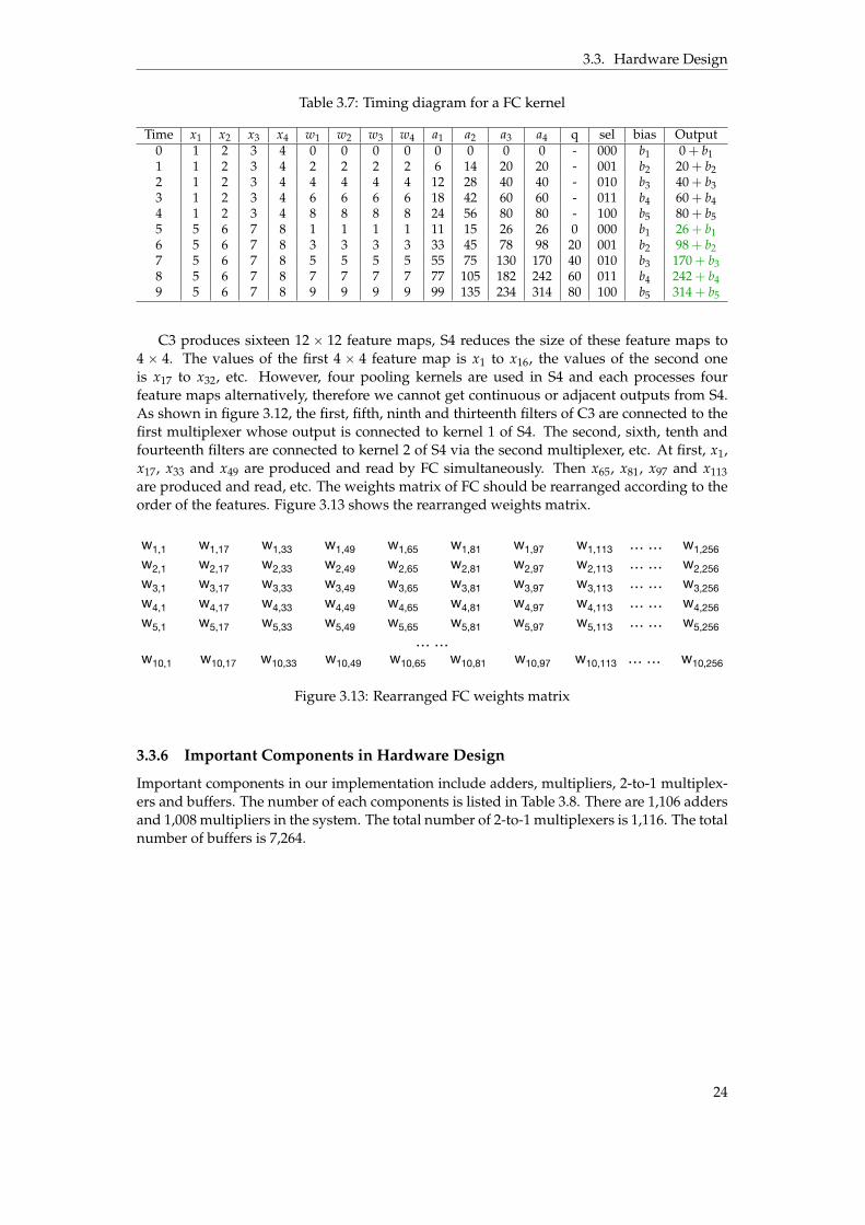
Table 3.1: Timing diagram for a C1 kernel
Time Input sel_1 sel_2 sel_3 a11 a12 a13 a21 a22 a23 a31 a32 a330 1 1 1 0 1 1 0 1 1 0 1 1 01 2 1 1 1 2 3 3 2 3 3 2 3 32 3 1 1 1 3 5 6 3 5 6 3 5 63 4 1 1 1 4 7 9 4 7 9 4 7 94 5 1 1 1 5 9 12 5 9 12 5 9 125 6 0 1 1 0 11 15 3 11 15 3 11 156 7 1 1 0 7 7 11 13 10 11 13 10 117 8 1 1 1 8 15 15 17 21 18 17 21 188 9 1 1 1 9 17 24 21 26 30 21 26 309 10 1 1 1 10 19 27 25 31 36 25 31 3610 11 1 1 1 11 21 30 22 36 42 22 36 4211 12 0 1 1 0 23 33 15 34 48 18 34 4812 13 1 1 0 13 13 23 37 28 34 43 31 3413 14 1 1 1 14 27 27 41 51 42 50 57 45
is read, a convolutional kernel has not produced all valid outputs, those outputs that are notproduced yet are actually calculated and stored in buffers. Since a convolutional kernel hasonly one output port, we need to push these values in sequence. During the idle time, thesel_1, sel_2, and sel_3 signals are set to 0. Therefore, the values held in buffers will be addedby zero and moved forward until they are output. The idle time is mˆ ( f ´ 1)/2 + ( f ´ 1)/2clock cycles, where m is the image size and f is the convolutional kernel size.
C1 consists of eight convolutional kernels that work in parallel. Thus eight feature mapsare produced simultaneously.
Input images are grayscale. Therefore the range of pixel values is between 0 and 255.Eight bits are enough to represent these pixel values. However, the convolution operationmay cause overflow if we use only eight bits word length for input images. As mentionedbefore, parameters in the network are ranged from -1 to 1, all pixels in a convolution windoware multiplied by the corresponding weights, and the multiplication results are summed up toproduce an output. In our case, 5ˆ 5 convolutional kernels are used in C1, thus 25 numbersare summed up. Let us assume that all pixels in a convolution window have the largestpossible value, i.e., 255, and all weights of the convolutional kernel have the largest possiblevalue, i.e., 1. The convolution result is calculated as: 255ˆ 1ˆ 5ˆ 5 = 6, 375. Therefore, 13bits are needed to represent the result. In order to avoid overflow, the word length of inputpixels is extended to 13 bits.
3.3.2 Pooling Layer S2
Max pooling is used in this thesis work. Pooling layer S2 uses 2ˆ2 pooling kernels. Figure 3.5shows the schematic of an S2 pooling kernel.
D MAX LD MAX D MAX Output
Input
a1 a2
Figure 3.5: Pooling kernel for S2
One pixel is read by an S2 kernel every clock cycle. The first input is stored in a bufferdenoted by D and delayed by one clock cycle, the next clock cycle the second input is com-
15

3.3. Hardware Design
pared with the first one that stored in the buffer. The larger value is stored in a long bufferdenoted by LD, the length of LD is computed as m´ f + 1 where m is the image size and fis the pooling kernel size. Then, the third input is compared with the partial result storedin LD, the larger value is again stored in a buffer and to be compared with the last input. Thefinal output is the maximum value in the pooling window. It takes m2 clock cycles for an S2kernel to finish one feature map, where m is the size of the input feature map. Consider themax pooling example in figure 2.6. Table 3.2 shows the timing diagram when an S2 kerneloperates on the image in figure 2.6. In the table, a1 and a2 are intermediate nodes shown infigure 3.5. The green numbers in the table are valid outputs.
Table 3.2: Time diagram for a S2 kernel
Time Input a1 a2 Output0 21 1 22 11 113 2 114 3 3 35 0 3 11 36 4 4 11 117 -1 4 3 118 0 0 3 39 3 3 4 3
10 1 3 4 411 2 2 2 412 -5 2 3 213 8 8 8 814 3 8 3 815 6 6 6 6
There are eight pooling kernels in S2 and each kernel applies a pooling operation on thefeature map generated by the corresponding convolutional kernel in C1. Since the frequencythat C1 produces outputs is the same as S2 reads inputs, i.e., one pixel every clock cycle, C1and S2 can be connected directly.
Since the pooling operation in S2 uses a stride of two pixels in both vertical and horizontaldirections, we cannot get valid outputs every clock cycle. However, the convolutional layerC3 needs to read an input every clock cycle. In order to synchronize the outputs of S2 andthe inputs of C3, FIFOs are needed between S2 and C3. Each S2 kernel is followed by a FIFO.
3.3.3 Convolutional Layer C3
The outputs of S2 are truncated to the same word length as the parameters of the network inorder to reduce hardware usage and computation efforts. For example, when we use 16 bitsto represent the parameters of the network, the outputs of S2 are truncated to 16 bits. If eightbits are used, then the outputs are truncated to eight bits.
As described in 2.5, a C3 filter convolves all eight feature maps produced by S2 and sumsthem up to generate a new feature map. If we use eight convolutional kernels shown in fig-ure 3.3 in parallel to build a filter of C3, the usage of logic resources will be high. Meanwhile,the depth of FIFOs between S2 and C3 will be large to ensure that C3 can read one pixel everyclock cycle. Therefore, a convolutional kernel can be reused to convolve several feature mapsby reading pixels from different FIFOs between S2 and C3 alternatively. According to thefrequency that S2 writes outputs to FIFOs, we decided to use two convolutional kernels tobuild a filter of C3, which means each kernel convolves four feature maps.
16

3.3. Hardware Design
Figure 3.6 shows the schematic of a C3 kernel. The structure of the convolutional kernelin this layer is similar to a C1 kernel shown in figure 3.3. The difference is that a C3 kernelreads data from different FIFOs alternatively and the coefficients are reloaded every clockcycle. The last three adders in the last row are used for summing four consecutive outputs.
4LD4D 4D
0 1 0 1
0
W(1,1) W(1,2) W(1,3)
0 1
4LD4D 4D
0 1 0 1
W(2,1) W(2,2) W(2,3)
0 1
4D 4D
0 1 0 1
W(3,1) W(3,2) W(3,3)
0 1
Output
sel_1 sel_2 sel_3
sel_1 sel_2 sel_3
sel_1 sel_2 sel_3
a11 a12 a13
a21 a22 a23
a31 a32 a33
FIFO 1FIFO 2FIFO 3FIFO 4
fifo_sel
00
01
10
11
Input
D D D
Figure 3.6: Convolutional kernel for C3
A 4-to-1 multiplexer is added at the input of a convolutional kernel. Four FIFOs betweenS2 and C3 are connected to the multiplexer. The short buffers 4D delay data by 4 clock cycles.The long buffers 4LD delay data by 4ˆ (m´ f ) where m is the input image size and f is theconvolutional kernel size.
Table 3.3 shows the timing diagram of the data streams between S2 and C3. The greennumbers are valid outputs of S2. S2_1_out, S2_2_out, S2_3_out and S2_4_out in the table referto the outputs of the first, the second, the third and the fourth S2 kernel respectively. fifo_wris the write-enable signal for all FIFOs between S2 and C3. fifo_1_rd, fifo_2_rd, fifo_3_rd andfifo_4_rd are the read-enable signals for FIFO 1 to 4 between S2 and C3. C3_fifo_sel is the selectsignal for the multiplexer. C3_input is the output of the multiplexer.
At t0 (time 0), an S2 kernel reads the first pixel. At t25 it produces the first valid output andthe fifo_wr signal becomes high. A valid output is produced every second clock cycle duringt25 and t47. Then fifo_wr remains low for 25 clock cycles. In other words, an S2 kernel producestwelve outputs in 48 clock cycles and repeats this procedure until it has read all pixels of afeature map produced by C1 and ReLU block. The read-enable signals for different FIFOsbecome high successively. Therefore, a C3 kernel reads a value from the same FIFO everyfourth clock cycles and all the values in the FIFO are read out before S2 starts to write to itagain. In this way, the depth of these FIFOs can be reduced to eight.
Consider the example in figure 3.7. Let us assume that the four 6ˆ 6 images in figure 3.7are stored in FIFOs. A C3 kernel reads from these FIFOs and convolves all the four images.The size of the convolutional kernel is 3ˆ 3. Four intermediate feature maps are produced bythe convolution operation, and they are summed up to produce a new feature map. Table 3.4shows the timing diagram when a C3 kernel operates on this example. The green number inthe table is a valid output of C3.
In each C3 filter, two convolutional kernels work in parallel and the results of two kernelsare summed up to produce a new feature map. FIFO 1 to 4 are mapped to the first kernel,
17

3.3. Hardware Design
Table 3.3: Data streams between S2 and C3
Time S2_1_out S2_2_out S2_3_out S2_4_out fifo_wr fifo_1_rd fifo_2_rd fifo_3_rd fifo_4_rd C3_fifo_sel C3_input0 x0_1 x0_2 x0_3 x0_4 0 0 0 0 0 - -1 x1_1 x1_2 x1_3 x1_4 0 0 0 0 0 - -2 x2_1 x2_2 x2_3 x2_4 0 0 0 0 0 - -... ... ... ... ... ... ... ... ... ... ... ...25 x25_1 x25_2 x25_3 x25_4 1 0 0 0 0 - -26 x26_1 x26_2 x26_3 x26_4 0 1 0 0 0 00 x25_127 x27_1 x27_2 x27_3 x27_4 1 0 1 0 0 01 x25_228 x28_1 x28_2 x28_3 x28_4 0 0 0 1 0 10 x25_329 x29_1 x29_2 x29_3 x29_4 1 0 0 0 1 11 x25_430 x30_1 x30_2 x30_3 x30_4 0 1 0 0 0 00 x27_131 x31_1 x31_2 x31_3 x31_4 1 0 1 0 0 01 x27_232 x32_1 x32_2 x32_3 x32_4 0 0 0 1 0 10 x27_333 x33_1 x33_2 x33_3 x33_4 1 0 0 0 1 11 x27_434 x34_1 x34_2 x34_3 x34_4 0 1 0 0 0 00 x29_135 x35_1 x35_2 x35_3 x35_4 1 0 1 0 0 01 x29_236 x36_1 x36_2 x36_3 x36_4 0 0 0 1 0 10 x29_337 x37_1 x37_2 x37_3 x37_4 1 0 0 0 1 11 x29_438 x38_1 x38_2 x38_3 x38_4 0 1 0 0 0 00 x31_139 x39_1 x39_2 x39_3 x39_4 1 0 1 0 0 01 x31_240 x40_1 x40_2 x40_3 x40_4 0 0 0 1 0 10 x31_341 x41_1 x41_2 x41_3 x41_4 1 0 0 0 1 11 x31_442 x42_1 x42_2 x42_3 x42_4 0 1 0 0 0 00 x33_143 x43_1 x43_2 x43_3 x43_4 1 0 1 0 0 01 x33_244 x44_1 x44_2 x44_3 x44_4 0 0 0 1 0 10 x33_345 x45_1 x45_2 x45_3 x45_4 1 0 0 0 1 11 x33_446 x46_1 x46_2 x46_3 x46_4 0 1 0 0 0 00 x35_147 x47_1 x47_2 x47_3 x47_4 1 0 1 0 0 01 x35_2
and FIFO 5 to 8 are mapped to the second. Similar to C1 filters, idle time for C3 filters is alsoneeded after C3 filters have read all inputs. The idle time is 4ˆmˆ ( f ´ 1)/2 + ( f ´ 1)/2clock cycles, where m is the input image size and f is the convolutional kernel size.
Each C3 filter produces a valid output every fourth clock cycles. The outputs of C3 arewritten into FIFOs because the next layer needs to read one value every clock cycle.
3.3.4 Pooling Layer S4
There are 16 filters in parallel in C3 and each filter generates one output every fourth clockcycle. If we use the same structure as the pooling kernel in S2, we need 16 such kernels inparallel which is inefficient. Meanwhile, if a pooling kernel reads an input every fourth clockcycle, it means the kernel is idle for three-quarters of the time which is a waste of energy.
In order to reduce the amount of hardware resources used and also reduce the idle timeof kernels, we use a slightly different structure to S2. Figure 3.8 shows the schematic of an S4kernel.
A 4-to-1 multiplexer is connected to the input of an S4 kernel. Four FIFOs between C3and S4 are connected to the inputs of the multiplexer. The short buffers denoted by 4D nowdelay the data by four clock cycles instead of one. The long buffers 4LD delay the data by4 ˆ (m ´ f + 1) clock cycles instead of m ´ f + 1, where m is the image size and f is thepooling kernel size. Each kernel reads data from FIFOs alternatively. In other words, eachkernel does pooling operation to four feature maps alternatively. Therefore, four poolingkernels are needed in S4.
Table 3.5 shows the timing diagram of the data streams between C3 and S4.The green numbers in the table are valid outputs of C3. C3_1_out, C3_2_out, C3_3_out
and C3_4_out are the outputs of 4 C3 filters. fifo_wr is the write-enable signal for all FIFOsbetween C3 and S4. fifo_1_rd, fifo_2_rd, fifo_3_rd and fifo_4_rd are the read-enable signals forFIFO 1 to 4 between C3 and S4. S4_fifo_sel is the select signal for the multiplexer. S4_input isthe output of the multiplexer. Every fourth clock cycles one valid outputs are produced byC3 and fifo_wr becomes high. Read-enable signal of the FIFOs become high successively inthe following four clock cycles. When read-enable signal of a FIFO is high, the multiplexerselects this FIFO. In this way each S4 kernel is never idle, thus fewer hardware resource isneeded.
18

3.3. Hardware Design
FIFO 1
00 0 000 00
0
0
0
0
0
0
0
0000 0 00
0
0
0
0
0
0
6
1615
22
35
5
36
27
2
37
21
33
9
19
20 25
34
11
24
28
4
12
7
31
18
26
13
3
32
14
8 10
29 30
17
23
FIFO 2
0
0
0
0
0
0
0
0
0
0
0
0
0
0
0
0
0
21
0
28
0
25
17
7
22
38
6
1411
26
0
19
0
10
16
0
36
2018
4
33
29
8
0
35
13
34
0
31
23
3
37
0
24
30 32
15
0
27
9 12
0
0
5
FIFO 3
0
0
0
0
0
0
0
0
0
0
0
0
0
0
0
0
16 17
0
0
30 31
26
35
21
24
5
3934
0
0 0
19
25
37
3329
15
27
14
23
0
38
9
0
28
84
18
10
0
0
20
0
6
0
22
36
32
12 13
0
11
7
FIFO 4
0
0
0
0
0
0
0
0
000 00 0 0
0
0
0
0
0
0
0
000 0 00
1 62 3 4 5
9 10 127 118
31
19
25
13
32
20
14
26
18
34
21
15 16
22 24
30
17
29
23
35
27
33
28
36
*(Stride = 1)
1
1
1
11
1
1 1
1
Convolutional Kernel
174 130180 192
36
114
180
18 48
261
207
243
126
186
30
198
42
177
135
99
117
72
189
153
234
81
153
9045
34
141
105
69
81
252
144
Intermediate Feature Map 1
*(Stride = 1)
1
1
1
11
1
1 1
1
Convolutional Kernel
*(Stride = 1)
1
1
1
11
1
1 1
1
Convolutional Kernel
*(Stride = 1)
1
1
1
11
1
1 1
1
Convolutional Kernel
111
147
38
134
183
75
118
159
87
123
51
22
192
162
216
180
99
243
207
42
135
48 54
186
189
261
153
81
144
36
198
90
270252
108
198
Intermediate Feature Map 2
42
81
138
189
153
117153
261
60
16293
186
216
165
192
117
48
270
144
10890
207
122
57
129
252
204
54
198
42
99
279
198 225
26
171
Intermediate Feature Map 3
46
87
123
142
195
159
261
99
270
192 198
279
66
171
225
99 117
126
60
216
126108
180
30
207
171
63
162
204 210
153
54
288
48
234135
Intermediate Feature Map 4
Σ 456
600
160
544
744
312
480
648
360
504
216
96
780
666
882
732
414
990
846
180
558
204 228
756
774
1062
630
342
594
156
804
378
10981026
450
810
New Feature Map
Figure 3.7: Four 6ˆ 6 images and a 3ˆ 3 convolutional kernel
4D MAX 4LD MAX 4D MAX Output
InputFIFO 1FIFO 2FIFO 3FIFO 4
fifo_sel
a1 a2
Figure 3.8: Pooling kernel for S4
Table 3.6 shows the timing diagram for the circuit shown in figure 3.8. To show the timingclearly, we use four feature maps shown in figure 3.9 as the inputs of the circuit.
The green numbers in Table 3.6 are valid outputs. As shown in the table, the S4 kernelproduces four valid outputs in a row during t_20 to t_23 and t_28 to t_31. The outputs arestored in FIFOs because the next layer reads data with a different frequency.
19

3.3. Hardware Design
Table 3.4: Timing diagram for a C3 kernel
Time fifo_sel Input sel_1 sel_2 sel_3 a11 a12 a13 a21 a22 a23 a31 a32 a33 Output0 00 1 1 1 0 1 1 0 1 1 0 1 1 01 01 2 1 1 0 2 2 0 2 2 0 2 2 02 10 3 1 1 0 3 3 0 3 3 0 3 3 03 11 4 1 1 0 4 4 0 4 4 0 4 4 0 04 00 2 1 1 1 2 3 3 2 3 3 2 3 3 35 01 3 1 1 1 3 5 5 3 5 5 3 5 5 86 10 4 1 1 1 4 7 7 4 7 7 4 7 7 157 11 5 1 1 1 5 9 9 5 9 9 5 9 9 248 00 3 1 1 1 3 5 6 3 5 6 3 5 6 279 01 4 1 1 1 4 7 9 4 7 9 4 7 9 3110 10 5 1 1 1 5 9 12 5 9 12 5 9 12 3611 11 6 1 1 1 6 11 15 6 11 15 6 11 15 4212 00 4 1 1 1 4 7 9 4 7 9 4 7 9 4513 01 5 1 1 1 5 9 12 5 9 12 5 9 12 4814 10 6 1 1 1 6 11 15 6 11 15 6 11 15 5115 11 7 1 1 1 7 13 18 7 13 18 7 13 18 5416 00 5 1 1 1 5 9 12 5 9 12 5 9 12 5717 01 6 1 1 1 6 11 15 6 11 15 6 11 15 6018 10 7 1 1 1 7 13 18 7 13 18 7 13 18 6319 11 8 1 1 1 8 15 21 8 15 21 8 15 21 6620 00 6 0 1 1 0 11 15 3 11 15 3 11 15 6921 01 7 0 1 1 0 13 18 5 13 18 5 13 18 7222 10 8 0 1 1 0 15 21 7 15 21 7 15 21 7523 11 9 0 1 1 0 17 24 0 17 24 0 17 24 7824 00 7 1 1 0 7 7 11 13 10 11 13 10 11 7425 01 8 1 1 0 8 8 13 17 13 13 17 13 13 6926 10 9 1 1 0 9 9 15 21 16 15 21 16 15 6327 11 10 1 1 0 10 10 17 25 19 17 25 19 17 5628 00 8 1 1 1 8 15 15 17 21 18 17 21 18 5329 01 9 1 1 1 9 17 17 21 26 22 21 26 22 7230 10 10 1 1 1 10 19 19 25 31 26 25 31 26 8331 11 11 1 1 1 11 21 21 29 36 30 29 36 30 96
Table 3.5: Data streams between C3 and S4
Time C3_1_out C3_2_out C3_3_out C3_4_out fifo_wr fifo_1_rd fifo_2_rd fifo_3_rd fifo_4_rd S4_fifo_sel S4_input0 x0_1 x0_2 x0_3 x0_4 1 0 0 0 0 - -1 x1_1 x1_2 x1_3 x1_4 0 1 0 0 0 00 x0_12 x2_1 x2_2 x2_3 x2_4 0 0 1 0 0 01 x0_23 x3_1 x3_2 x3_3 x3_4 0 0 0 1 0 10 x0_34 x4_1 x4_2 x4_3 x4_4 1 0 0 0 1 11 x0_45 x5_1 x5_2 x5_3 x5_4 0 1 0 0 0 00 x4_16 x6_1 x6_2 x6_3 x6_4 0 0 1 0 0 01 x4_27 x7_1 x7_2 x7_3 x7_4 0 0 0 1 0 10 x4_38 x8_1 x8_2 x8_3 x8_4 1 0 0 0 1 11 x4_49 x9_1 x9_2 x9_3 x9_4 0 1 0 0 0 00 x8_110 x10_1 x10_2 x10_3 x10_4 0 0 1 0 0 01 x8_211 x11_1 x11_2 x11_3 x11_4 0 0 0 1 0 10 x8_312 x12_1 x12_2 x12_3 x12_4 1 0 0 0 1 11 x8_413 x13_1 x13_2 x13_3 x13_4 0 1 0 0 0 00 x12_114 x14_1 x14_2 x14_3 x14_4 0 0 1 0 0 01 x12_215 x15_1 x15_2 x15_3 x15_4 0 0 0 1 0 10 x12_316 x16_1 x16_2 x16_3 x16_4 1 0 0 0 1 11 x12_4
3.3.5 Fully Connected Layer
There are four pooling kernels in S4. Each S4 kernel produces four 4ˆ 4 feature maps thus16 feature maps are produced in total. All the outputs of S4 are written into FIFOs beforethey are read by the FC layer. All 16 feature maps are flattened and combined to create avector of 256 elements. The FC layer takes this vector as its input and multiplies it with the10ˆ 256 weight matrix. All the values of this vector are truncated to the same word length asthe parameters in the network due to the same reason described in section 3.3.3.
20

3.3. Hardware Design
8
2-23
5-14
1
60
0
67-2
41
7
156
43-1
0
14
1
56-1
32
4
4-23
-785
-2
75
2
150
33
9
3-34
801
9
51
3
187
03
Feature map 1 Feature map 2 Feature map 3 Feature map 4
Figure 3.9: 4ˆ 4 feature maps
Table 3.6: Timing diagram for a S4 kernel
Time fifo_sel Input a1 a2 Output0 00 -11 01 32 10 83 11 04 00 2 25 01 1 36 10 4 87 11 3 38 00 5 59 01 4 410 10 -7 411 11 8 812 00 1 513 01 0 414 10 -2 -215 11 9 916 00 4 4 417 01 -1 0 318 10 5 5 819 11 1 9 320 00 3 4 5 421 01 6 6 6 622 10 3 5 4 823 11 4 4 8 424 00 0 3 5 525 01 1 6 4 626 10 2 3 2 427 11 3 4 9 828 00 -2 0 4 529 01 5 5 5 530 10 -2 2 5 231 11 -3 3 9 9
Our strategy to design an FC kernel is to read four inputs from four FIFOs simultaneouslyand make them stationary in register file for several clock cycles and reload the correspondingweights of different rows alternatively. After these four inputs are multiplied by the corre-sponding weights of the last row, the FC kernel reads the next four inputs and repeats theprocedure until all inputs are read. The most resource-efficient way is to use only one FCkernel. Four inputs are held in register file for ten clock cycles, and they are multiplied witheach row of the weight matrix. In this case, it takes (256/4)ˆ 10 = 640 clock cycles to finishthe vector-matrix multiplication. The throughput of the FC layer could be improved by usingmultiple kernels in parallel. To have good load balancing among kernels, we could use two
21

3.3. Hardware Design
kernels, five kernels and ten kernels in parallel. However, hardware usage increases with thenumber of kernels.
In order to reduce hardware usage and reduce inference time, we use two FC kernels andeach of them calculates five outputs. Figure 3.10 shows the schematic of an FC kernel.
x1 x2 x3 x4
b2b1
b3b4b5
Output
w1 w2 w3 w4
FIFO
adder_1 adder_2
adder_3
adder_4
adder_5
sel
a1 a2
a3
a4
bias
q000001010011100
Figure 3.10: FC Kernel
As shown in figure 3.10, four inputs x1, x2, x3 and x4 are read simultaneously and multi-plied by the weights w1, w2, w3 and w4 respectively. w1 to w4 are changed every clock cycle.The products are summed by adders. The length of the FIFO is five. adder_5 is used foradding bias. A 5-to-1 multiplexer is connected to adder_5 to select bias. We use an exampleto show the timing of an FC kernel. Figure 3.11 shows the matrix and the vector that the FCkernel operates on. Table 3.7 shows the timing diagram.
0 0 0 0 1 1 1 1
2 2 2 2 3 3 3 3
4 4 4 4 5 5 5 5
6 6 6 6 7 7 7 7
8 8 8 8 9 9 9 9
12345678
*
5 x 8 matrix 8 x 1 vector
Figure 3.11: 5ˆ 8 matrix and 8ˆ 1 vector
At t0, the FC kernel reads the first four values of the vector. The first four weights of thefirst row are also read at t0. In the following four clock cycles, the first four weights of rowtwo to five are read successively. At t5, the next four values of the vector are read. The nextfour weights of row one to five are read during t5 to t9. When the kernel reads weights froma certain row, the bias of that row is also read. The green numbers in the table are the finaloutputs.
Note that the weight matrix has to be rearranged to get the correct result since the fourinputs of the FC layer are not adjacent. The weight matrix should be rearranged according tothe connectivity between C3 and S4. See figure 3.12.
22

3.3. Hardware Design
X6
X1
X10
X5
X2
X3
X7
X15
X13
X11
X4
X8
X16
X12
X14
X9
1st feature map produced by C
3
12345
… …
S4 kernel 1
S4 kernel 2
S4 kernel 3
S4 kernel 4
67816
……
X194 X
130 X66 X
2 X193 X
129 X65 X
1
……
X210 X
146 X82 X
18 X209 X
145 X81 X
17
……
X226 X
162 X98 X
34 X225 X
161 X97 X
33
……
X242 X
178 X114 X
50 X241 X
177 X113 X
49
Figure3.12:C
onnectivitybetw
eenC
3and
S4
23
3.3. Hardware Design
Table 3.7: Timing diagram for a FC kernel
Time x1 x2 x3 x4 w1 w2 w3 w4 a1 a2 a3 a4 q sel bias Output0 1 2 3 4 0 0 0 0 0 0 0 0 - 000 b1 0 + b11 1 2 3 4 2 2 2 2 6 14 20 20 - 001 b2 20 + b22 1 2 3 4 4 4 4 4 12 28 40 40 - 010 b3 40 + b33 1 2 3 4 6 6 6 6 18 42 60 60 - 011 b4 60 + b44 1 2 3 4 8 8 8 8 24 56 80 80 - 100 b5 80 + b55 5 6 7 8 1 1 1 1 11 15 26 26 0 000 b1 26 + b16 5 6 7 8 3 3 3 3 33 45 78 98 20 001 b2 98 + b27 5 6 7 8 5 5 5 5 55 75 130 170 40 010 b3 170 + b38 5 6 7 8 7 7 7 7 77 105 182 242 60 011 b4 242 + b49 5 6 7 8 9 9 9 9 99 135 234 314 80 100 b5 314 + b5
C3 produces sixteen 12ˆ 12 feature maps, S4 reduces the size of these feature maps to4 ˆ 4. The values of the first 4 ˆ 4 feature map is x1 to x16, the values of the second oneis x17 to x32, etc. However, four pooling kernels are used in S4 and each processes fourfeature maps alternatively, therefore we cannot get continuous or adjacent outputs from S4.As shown in figure 3.12, the first, fifth, ninth and thirteenth filters of C3 are connected to thefirst multiplexer whose output is connected to kernel 1 of S4. The second, sixth, tenth andfourteenth filters are connected to kernel 2 of S4 via the second multiplexer, etc. At first, x1,x17, x33 and x49 are produced and read by FC simultaneously. Then x65, x81, x97 and x113are produced and read, etc. The weights matrix of FC should be rearranged according to theorder of the features. Figure 3.13 shows the rearranged weights matrix.
w1,1 w1,17 w1,33 w1,49 w1,65 w1,81 w1,97 w1,113 … … w1,256w2,1 w2,17 w2,33 w2,49 w2,65 w2,81 w2,97 w2,113 … … w2,256w3,1 w3,17 w3,33 w3,49 w3,65 w3,81 w3,97 w3,113 … … w3,256w4,1 w4,17 w4,33 w4,49 w4,65 w4,81 w4,97 w4,113 … … w4,256w5,1 w5,17 w5,33 w5,49 w5,65 w5,81 w5,97 w5,113 … … w5,256
… …w10,1 w10,17 w10,33 w10,49 w10,65 w10,81 w10,97 w10,113 … … w10,256
Figure 3.13: Rearranged FC weights matrix
3.3.6 Important Components in Hardware Design
Important components in our implementation include adders, multipliers, 2-to-1 multiplex-ers and buffers. The number of each components is listed in Table 3.8. There are 1,106 addersand 1,008 multipliers in the system. The total number of 2-to-1 multiplexers is 1,116. The totalnumber of buffers is 7,264.
24

3.3. Hardware Design
Table 3.8: Number of components in the design
Layer HardwareComponent
#ComponentPer Module
#Modulesin Parallel
Total Numberof Components
C1
Adder 25
8
200Multiplier 25 2002-to-1 Mux 25 200
Buffer 96 768
S2
Adder 0
8
0Multiplier 0 02-to-1 Mux 0 0
Buffer 25 200
C3
Adder 56
16
896Multiplier 50 8002-to-1 Mux 56 896
Buffer 387 6,192
S4
Adder 0
4
0Multiplier 0 02-to-1 Mux 3 12
Buffer 26 104
FC
Adder 5
2
10Multiplier 4 82-to-1 Mux 4 8
Buffer 0 0
25

4 Results and Discussion
The software model is implemented on a CPU (Intel Core i7-8750H, 2.20 GHz) and a GPU(Nvidia GeForce GTX 1060) respectively. The hardware design is implemented on Intel Arria5AGZME3E2H29C3 FPGA. Both software and hardware design are tested. The test resultsare presented in this chapter.
We will discuss the method we used during implementation, the results we obtained andwhat can be done to improve the design.
4.1 Resources Utilization
The FPGA operates at 100 MHz. The maximum frequency (Fmax) the FPGA can run at is102.3 MHz. The critical path that limits the Fmax is from the control logic to the FIFOs be-tween S2 and C3.
Table 4.1 shows the resource utilization of the FPGA (using 16-bits fixed-point to representthe network’s parameters).
Table 4.1: FPGA resources utilization
Resource ALMs used forLUT and registers
ALMs used forLUT
ALMs used forregisters
Total ALMs(after packing) LUT Register DSP BRAM(M20K)
Used 4,925 4,153 100,013 57,662 9,078 210,364 988 30Available 135,840 135,840 135,840 135,840 135,840 543,360 1,044 957
Utilization 4% 3% 74% 42% 7% 39% 95% 3%
Each adaptive logic module (ALM) on the FPGA has an 8-input adaptive look up table(LUT) and four registers [43]. The design consumes 42% of ALMs after Quartus performspacking. The utilization of 8-input LUTs is around 7%. The utilization of registers is closeto ALMs since most ALMs are used for registers. As mentioned in section 3.3.6, there are1,008 multipliers in the design. All the multipliers are mapped to hard-core DSP blocks. EachDSP block on this FPGA has two 18ˆ 18 multipliers [43]. Most DSP blocks have only onemultiplier mapped to each of them, however, in some parts of the design two multipliersare mapped to a single DSP block for optimization purpose. For example, in an FC kernel,the first two multipliers are mapped to the same DSP block, and the second two are mappedto the same DSP block. Therefore, the number of DSP blocks used is slightly less than the
26

4.2. Accuracy
Table 4.2: Accuracy of the implementation
Software(floating point) 5 bits 6 bits 7 bits 8 bits 9 bits 10 bits 11 bits 12 bits 13 bits 14 bits 15 bits 16 bits
Accuracy compared tosoftware implementation (%) / 43.30 95.44 98.93 99.59 99.83 99.93 99.96 99.99 100 100 100 100
Accuracy compared toreal value (%) 98.81 43.30 95.53 98.48 98.76 98.80 98.78 98.81 98.82 98.81 98.81 98.81 98.81
number of multipliers in the design. The usage of block memory (BRAM) is relatively lowsince only the network’s parameters are stored on-chip.
4.2 Accuracy
Both software and hardware implementations are tested with the test set in the MNISTdatabase, which contains 10,000 images. The software model has a 98.81% inference accu-racy. Table 4.2 shows how the accuracy of the hardware implementation affected by the wordlength of parameters. Figure 4.1 shows the trend.
0
25
50
75
100
5 6 7 8 9 10 11 12 13 14 15
Accu
racy
word length
Accuracy compared to software Accuracy compared to real value
Figure 4.1: Accuracy of the implementation
The accuracy of the software model is 98.81%. The accuracy of the hardware implemen-tation compared to software model is computed as
Accuracy(compared to so f tware) = 1´Number o f wrong prediction(compared to so f tware)
Total number o f test samples(4.1)
The accuracy compared to real value is computed as
Accuracy(compared to real value) = 1´Number o f wrong prediction(compared to MNIST)
Total number o f test samples(4.2)
In Table 4.2 we can see that the accuracy of the FPGA implementation is affected bythe word length of fixed-point arithmetic. There is no accuracy loss (compared to softwaremodel) when word length reduces from 16 bits to 13 bits. Shorter word length means fewerhardware resources usage and lower power consumption. Using fixed-point arithmetic andadjust word length according to specific requirements can be helpful in power-critical appli-cations.
27

4.3. Runtime and Throughput
Table 4.3: Software and hardware inference of the same image
Out_0 Out_1 Out_2 Out_3 Out_4 Out_5 Out_6 Out_7 Out_8 Out_9Software -1,366.2 -2,117.3 -560.8 -319.5 2,883.3 -1,839.7 -1,842.0 -109.3 1,563.4 2,758.510-bits
fixed-point -1308.4 -2123.5 -574.4 -276.8 2,829.5 -1,815.5 -1,798.7 -159.3 1,547.3 2,785.9
9-bitsfixed-point -1,347.5 -2,103.5 -693.7 288.3 2,764.3 -1,815.3 -1,739.2 -133.8 1,486.0 2,942.8
However, it is worth trying to use floating-point arithmetic on FPGA since floating-pointarithmetic has higher precision thus provides the better accuracy. Some accuracy-critical ap-plications such as face-recognition and digits-recognition can especially benefit from floating-point arithmetic.
Note that the accuracy (compared to real value) drops slightly when the word length in-creases from 9 to 10, this also happens when the word length changes from 12 to 13. Thereason is that the software model fails to recognize some digits, however, the hardware im-plementation happens to make the correct inference with degraded precision. For instance,figure 4.2 shows an image from the MNIST database. This image is marked as 9 by thedatabase. Table 4.3 lists the inference results on this image made by software and hardware.
5 10 15 20
5
10
15
20
Figure 4.2: An image from MNIST database
The index of the largest number of each row in the table is the predicted result. Thesoftware makes an inference that the digit is 4 which is not correct. The hardware imple-mentation with 10-bits weights also makes the same inference. However, with a degradedprecision, 9-bits implementation happens to make the correct inference.
4.3 Runtime and Throughput
Table 4.4 lists the runtime and throughput of different platforms.
Table 4.4: Performance of different platforms
Device CPU GPU FPGARuntime for 10,000 images (s) 1.680 1.990 0.068
Runtime per image (µs) 168.0 199.0 6.8Throughput (images/s) 5.95k 5.02k 147.06k
When we test the software model with all the 10,000 images in the test set, the GPU takesthe longest time which is 1.99 s. The FPGA takes 680 clock cycles to make an inference and itis capable of processing continuously, thus it takes 0.068 s to finish 10,000 images. The CPUperforms slightly better than the GPU. However, when we increase the number of samplesin the test, the GPU begins to show its advantages over the CPU. Table 4.5 shows how theruntime of different platforms changes with the increase of the number of samples. Figure 4.3shows the trend.
As shown in Table 4.5 and figure 4.3, the runtime of the GPU decreases with the increasingnumber of samples while the runtime of the CPU remains stable at about 170 us. However,
28
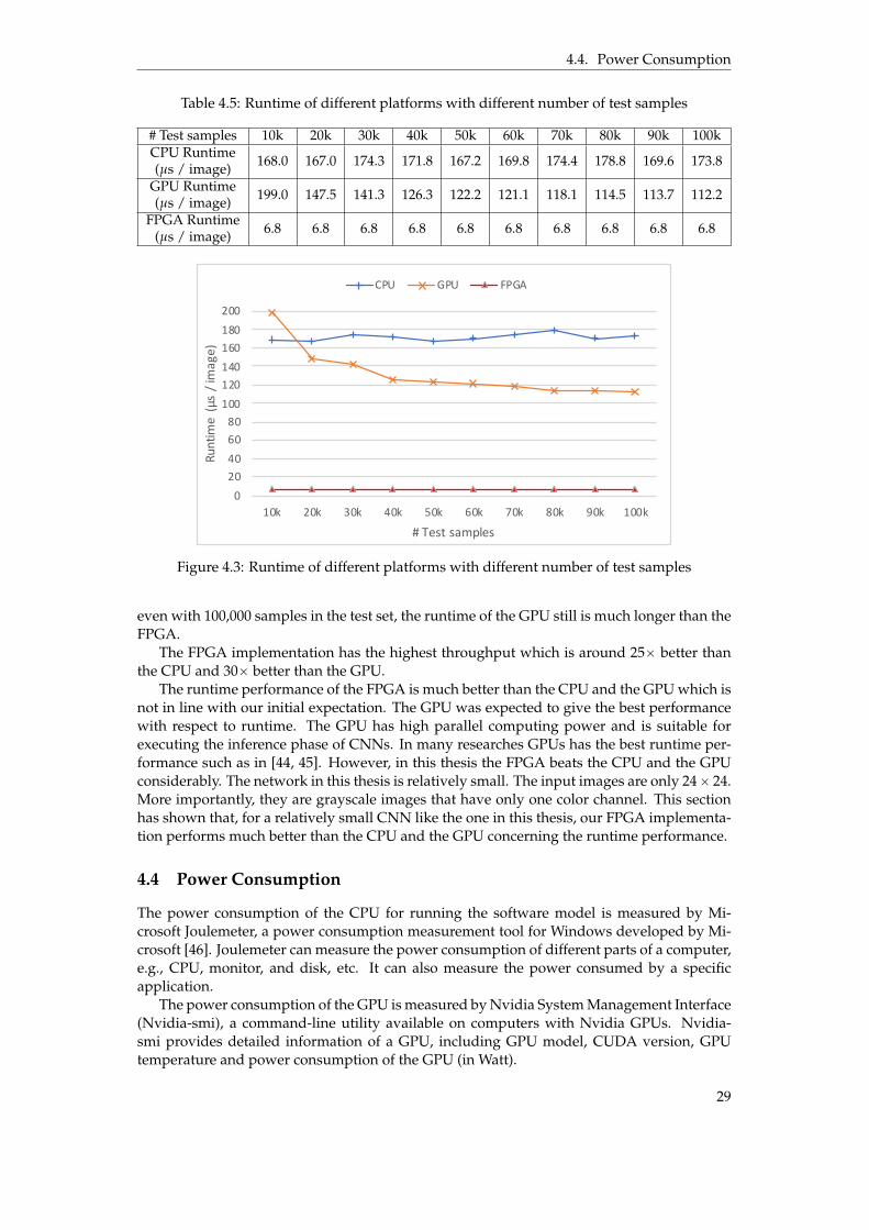
4.4. Power Consumption
Table 4.5: Runtime of different platforms with different number of test samples
# Test samples 10k 20k 30k 40k 50k 60k 70k 80k 90k 100kCPU Runtime(µs / image) 168.0 167.0 174.3 171.8 167.2 169.8 174.4 178.8 169.6 173.8
GPU Runtime(µs / image) 199.0 147.5 141.3 126.3 122.2 121.1 118.1 114.5 113.7 112.2
FPGA Runtime(µs / image) 6.8 6.8 6.8 6.8 6.8 6.8 6.8 6.8 6.8 6.8
020406080
100120140160180200
10k 20k 30k 40k 50k 60k 70k 80k 90k 100k
Runt
ime
(μs
/ im
age)
# Test samples
CPU GPU FPGA
Figure 4.3: Runtime of different platforms with different number of test samples
even with 100,000 samples in the test set, the runtime of the GPU still is much longer than theFPGA.
The FPGA implementation has the highest throughput which is around 25ˆ better thanthe CPU and 30ˆ better than the GPU.
The runtime performance of the FPGA is much better than the CPU and the GPU which isnot in line with our initial expectation. The GPU was expected to give the best performancewith respect to runtime. The GPU has high parallel computing power and is suitable forexecuting the inference phase of CNNs. In many researches GPUs has the best runtime per-formance such as in [44, 45]. However, in this thesis the FPGA beats the CPU and the GPUconsiderably. The network in this thesis is relatively small. The input images are only 24ˆ 24.More importantly, they are grayscale images that have only one color channel. This sectionhas shown that, for a relatively small CNN like the one in this thesis, our FPGA implementa-tion performs much better than the CPU and the GPU concerning the runtime performance.
4.4 Power Consumption
The power consumption of the CPU for running the software model is measured by Mi-crosoft Joulemeter, a power consumption measurement tool for Windows developed by Mi-crosoft [46]. Joulemeter can measure the power consumption of different parts of a computer,e.g., CPU, monitor, and disk, etc. It can also measure the power consumed by a specificapplication.
The power consumption of the GPU is measured by Nvidia System Management Interface(Nvidia-smi), a command-line utility available on computers with Nvidia GPUs. Nvidia-smi provides detailed information of a GPU, including GPU model, CUDA version, GPUtemperature and power consumption of the GPU (in Watt).
29

4.4. Power Consumption
We use PowerPlay Power Analyzer [47] in Quartus 15.1 to estimate the power consump-tion of the FPGA. According to [47], the accuracy of power estimation using PowerPlayPower Analyzer is ˘20% from silicon. To run power estimation with PowerPlay PowerAnalyzer, a Value Change Dump file (VCD) should be generated first by electronic designautomation (EDA) tools. A VCD file contains information about how a signal changes. Inthis thesis, we use ModelSim-SE to run gate-level simulations of the design. A VCD file thatcontains value change information of all signals and variables is generated by ModelSim-SEduring the simulation. Next, PowerPlay Power Analyzer reads VCD file and then computesthe toggle rates of all signals in the system based on the VCD file. Then PowerPlay PowerAnalyzer estimates the power consumption based on toggle rates and the information of thetarget device. Figure 4.4 is the power estimation report generated by PowerPlay Power An-alyzer. The PowerPlay Power Analyzer has high confidence in the estimation since we haveprovided sufficient toggle rate data, therefore it is reasonable to trust this estimation.
Figure 4.4: Power estimation report of the FPGA
Table 4.6 compares the power consumption of the CPU, GPU and FPGA.
Table 4.6: Power consumption of the the CPU, GPU and FPGA
Device CPU GPU FPGA(16-bits fixed point)Power (W) 25.4 23 4.2
The CPU consumes the highest power for running the software model, the GPU has aslightly lower power consumption compared to the CPU. The FPGA consumes the lowestpower which is 16.5% of CPU and 18.3% of GPU.
Figure 4.5 shows the power consumption and throughput of the CPU, GPU, and FPGA.The FPGA has the highest throughput but consumes the least power. Therefore the FPGAimplementation has the best efficiency. Table 4.7 lists the power efficiency of the three plat-forms. The power efficiency is computed as the number of operations per second per Watt(ops/s/W).
Table 4.7: Power efficiency
Device CPU GPU FPGAPower efficiency
(Gops/s/W) 0.29 0.27 43.29
The power efficiency of FPGA is around 149ˆ better than CPU and 160ˆ better than GPU.High power efficiency makes FPGA suitable for power-critical applications, and especiallysuitable for small CNNs. One of the future work could be implementing a larger CNN onCPUs, GPUs, and FPGAs respectively and see if our implementation still has better powerefficiency.
30
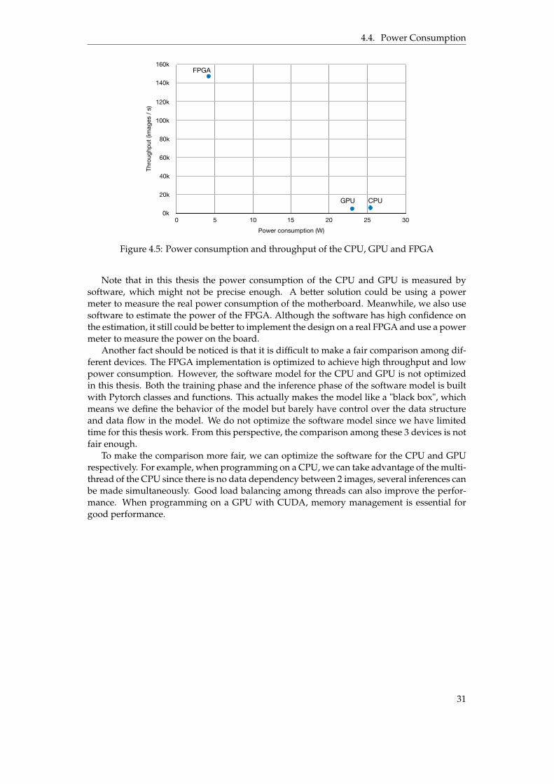
4.4. Power Consumption
ᤒ໒ 1
fpga 4.2 147.060
cpu 25.4 5.950
gpu 23 5.020
Thro
ughp
ut (i
mag
es /
s)
0k
20k
40k
60k
80k
100k
120k
140k
160k
Power consumption (W)0 5 10 15 20 25 30
FPGA
GPU CPU
�1
Figure 4.5: Power consumption and throughput of the CPU, GPU and FPGA
Note that in this thesis the power consumption of the CPU and GPU is measured bysoftware, which might not be precise enough. A better solution could be using a powermeter to measure the real power consumption of the motherboard. Meanwhile, we also usesoftware to estimate the power of the FPGA. Although the software has high confidence onthe estimation, it still could be better to implement the design on a real FPGA and use a powermeter to measure the power on the board.
Another fact should be noticed is that it is difficult to make a fair comparison among dif-ferent devices. The FPGA implementation is optimized to achieve high throughput and lowpower consumption. However, the software model for the CPU and GPU is not optimizedin this thesis. Both the training phase and the inference phase of the software model is builtwith Pytorch classes and functions. This actually makes the model like a "black box", whichmeans we define the behavior of the model but barely have control over the data structureand data flow in the model. We do not optimize the software model since we have limitedtime for this thesis work. From this perspective, the comparison among these 3 devices is notfair enough.
To make the comparison more fair, we can optimize the software for the CPU and GPUrespectively. For example, when programming on a CPU, we can take advantage of the multi-thread of the CPU since there is no data dependency between 2 images, several inferences canbe made simultaneously. Good load balancing among threads can also improve the perfor-mance. When programming on a GPU with CUDA, memory management is essential forgood performance.
31

5 Conclusion and Future Work
5.1 Conclusion
In this thesis, the inference phase of a digits recognition CNN has been implemented on anIntel Arria V FPGA. The system is optimized to achieve high throughput and low power con-sumption. The same CNN model is also implemented on a CPU and a GPU. The performanceof the CPU, GPU and FPGA are compared.
The FPGA implementation is pipelined to improve throughput. Fixed-point arithmetic isused to reduce hardware usage.
The FPGA implementation provides 100% inference accuracy with 13-bits or larger wordlengths. The FPGA achieves a throughput of 147,060 images/s, which is the highest amongthe 3 platforms. The FPGA has the best power efficiency (43.29 Gops/s/W), which is 149ˆbetter than the CPU and 160ˆ better than the GPU.
5.2 Answer to Research Questions
• Can FPGA implementation provide good performance with respect to inference accuracy?
Our FPGA implementation provides high accuracy for making inference. There is noaccuracy loss when we use 13-bits and longer word length fixed-point numbers.
• How fast can the implementation be to make a inference? Is it comparable to CPUs and GPUs?
It takes 6.8µs for the FPGA to make an inference. The CPU and the GPU spend 168µs and199µs respectively, to make an inference. The runtime performance of the FPGA is 25ˆ betterthan the CPU and 30ˆ better than the GPU. As discussed in chapter 4, we have proved thatthe FPGA implementation outperforms the CPU and the GPU for relatively small CNNs.
• How much is the power consumption of the CPU, GPU and FPGA? Which device has betterperformance and which one is more power-efficient?
The power consumption of the CPU, GPU and FPGA is listed in Table 4.6. The FPGAimplementation consumes the lowest power among the 3 devices. The FPGA also has thebest power efficiency as shown in Table 4.7.
32

5.3. Future Work
5.3 Future Work
The first thing we could do in the future is to implement the design on a real FPGA. In thatway, we could measure the performance more precisely. We can also have a camera connectedto the board and make real-time inference. However, very few cameras can generate imagesat the speed that the FPGA processes images. Therefore, another work can be done in thefuture is to sacrifice some throughput to further reduce the power consumption of the FPGA.
We have started with digits recognition because it is a relatively simple problem. In thefuture, we can extend the ideas in this thesis to address more complex CNNs such as facerecognition and object detection.
33

Bibliography
[1] Alex Krizhevsky, Ilya Sutskever, and Geoffrey E Hinton. “ImageNet Classification withDeep Convolutional Neural Networks”. In: Advances in Neural Information ProcessingSystems 25. Ed. by F. Pereira, C. J. C. Burges, L. Bottou, and K. Q. Weinberger. CurranAssociates, Inc., 2012, pp. 1097–1105. URL: http://papers.nips.cc/paper/4824- imagenet- classification- with- deep- convolutional- neural-networks.pdf.
[2] Fausto Milletari, Nassir Navab, and Seyed-Ahmad Ahmadi. “V-net: Fully convolu-tional neural networks for volumetric medical image segmentation”. In: 2016 FourthInternational Conference on 3D Vision (3DV). IEEE. 2016, pp. 565–571.
[3] Anil K Jain and Stan Z Li. Handbook of face recognition. Springer, 2011.
[4] Yann LeCun, Léon Bottou, Yoshua Bengio, Patrick Haffner, et al. “Gradient-based learn-ing applied to document recognition”. In: Proceedings of the IEEE 86.11 (1998), pp. 2278–2324.
[5] Teng Wang, Chao Wang, Xuehai Zhou, and Huaping Chen. “A Survey of FPGABased Deep Learning Accelerators: Challenges and Opportunities”. In: arXiv preprintarXiv:1901.04988 (2018).
[6] Chen Zhang, Peng Li, Guangyu Sun, Yijin Guan, Bingjun Xiao, and Jason Cong. “Op-timizing FPGA-based accelerator design for deep convolutional neural networks”. In:Proceedings of the 2015 ACM/SIGDA International Symposium on Field-Programmable GateArrays. ACM. 2015, pp. 161–170.
[7] Kalin Ovtcharov, Olatunji Ruwase, Joo-Young Kim, Jeremy Fowers, Karin Strauss, andEric S Chung. “Accelerating deep convolutional neural networks using specializedhardware”. In: Microsoft Research Whitepaper 2.11 (2015), pp. 1–4.
[8] Jiantao Qiu, Jie Wang, Song Yao, Kaiyuan Guo, Boxun Li, Erjin Zhou, Jincheng Yu,Tianqi Tang, Ningyi Xu, Sen Song, et al. “Going deeper with embedded FPGA platformfor convolutional neural network”. In: Proceedings of the 2016 ACM/SIGDA InternationalSymposium on Field-Programmable Gate Arrays. ACM. 2016, pp. 26–35.
[9] Naveen Suda, Vikas Chandra, Ganesh Dasika, Abinash Mohanty, Yufei Ma, SarmaVrudhula, Jae-sun Seo, and Yu Cao. “Throughput-optimized OpenCL-based FPGAaccelerator for large-scale convolutional neural networks”. In: Proceedings of the 2016
34

Bibliography
ACM/SIGDA International Symposium on Field-Programmable Gate Arrays. ACM. 2016,pp. 16–25.
[10] Ritchie Zhao, Weinan Song, Wentao Zhang, Tianwei Xing, Jeng-Hau Lin, Mani Sri-vastava, Rajesh Gupta, and Zhiru Zhang. “Accelerating binarized convolutionalneural networks with software-programmable FPGAs”. In: Proceedings of the 2017ACM/SIGDA International Symposium on Field-Programmable Gate Arrays. ACM. 2017,pp. 15–24.
[11] Karl Pauwels, Matteo Tomasi, Javier Diaz Alonso, Eduardo Ros, and Marc M Van Hulle.“A comparison of FPGA and GPU for real-time phase-based optical flow, stereo, andlocal image features”. In: IEEE Transactions on Computers 61.7 (2012), pp. 999–1012.
[12] John J Hopfield. “Artificial neural networks”. In: IEEE Circuits and Devices Magazine 4.5(1988), pp. 3–10.
[13] Vivienne Sze, Yu-Hsin Chen, Tien-Ju Yang, and Joel S Emer. “Efficient processing ofdeep neural networks: A tutorial and survey”. In: Proceedings of the IEEE 105.12 (2017),pp. 2295–2329.
[14] David Livingstone. Artificial neural networks: methods and applications. Springer, 2008.
[15] John Hertz, Anders Krogh, Richard G Palmer, and Heinz Horner. “Introduction to thetheory of neural computation”. In: Physics Today 44 (1991), p. 70.
[16] SN Sivanandam and SN Deepa. Introduction to neural networks using Matlab 6.0. TataMcGraw-Hill Education, 2006.
[17] Alex Krizhevsky, Ilya Sutskever, and Geoffrey E Hinton. “Imagenet classification withdeep convolutional neural networks”. In: Advances in neural information processing sys-tems. 2012, pp. 1097–1105.
[18] Vinod Nair and Geoffrey E Hinton. “Rectified linear units improve restricted Boltz-mann machines”. In: Proceedings of the 27th International Conference on Machine Learning(ICML-10). 2010, pp. 807–814.
[19] John S Bridle. “Probabilistic interpretation of feedforward classification network out-puts, with relationships to statistical pattern recognition”. In: Neurocomputing. Springer,1990, pp. 227–236.
[20] Bing Xu, Naiyan Wang, Tianqi Chen, and Mu Li. “Empirical evaluation of rectifiedactivations in convolutional network”. In: arXiv preprint arXiv:1505.00853 (2015).
[21] Carl Edward Rasmussen. “Gaussian processes in machine learning”. In: Summer Schoolon Machine Learning. Springer. 2003, pp. 63–71.
[22] Kevin P Murphy. Machine learning: a probabilistic perspective. MIT press, 2012.
[23] Daniel Svozil, Vladimir Kvasnicka, and Jiri Pospichal. “Introduction to multi-layerfeed-forward neural networks”. In: Chemometrics and Intelligent Laboratory Systems 39.1(1997), pp. 43–62.
[24] Quoc V Le et al. “A tutorial on deep learning part 2: Autoencoders, convolutional neu-ral networks and recurrent neural networks”. In: Google Brain (2015), pp. 1–20.
[25] Dominik Scherer, Andreas Müller, and Sven Behnke. “Evaluation of pooling opera-tions in convolutional architectures for object recognition”. In: International Conferenceon Artificial Neural Networks. Springer. 2010, pp. 92–101.
[26] Clément Farabet, Cyril Poulet, Jefferson Y Han, and Yann LeCun. “Cnp: An FPGA-based processor for convolutional networks”. In: 2009 International Conference on FieldProgrammable Logic and Applications. IEEE. 2009, pp. 32–37.
[27] Jinhwan Park and Wonyong Sung. “FPGA based implementation of deep neural net-works using on-chip memory only”. In: 2016 IEEE International Conference on Acoustics,Speech and Signal Processing (ICASSP). IEEE. 2016, pp. 1011–1015.
35

Bibliography
[28] Yufei Ma, Yu Cao, Sarma Vrudhula, and Jae-sun Seo. “Optimizing loop operation anddataflow in FPGA acceleration of deep convolutional neural networks”. In: Proceed-ings of the 2017 ACM/SIGDA International Symposium on Field-Programmable Gate Arrays.ACM. 2017, pp. 45–54.
[29] Yu-Hsin Chen, Joel Emer, and Vivienne Sze. “Eyeriss: A spatial architecture for energy-efficient dataflow for convolutional neural networks”. In: ACM SIGARCH ComputerArchitecture News. Vol. 44. 3. IEEE Press. 2016, pp. 367–379.
[30] Vinay Sriram, David Cox, Kuen Hung Tsoi, and Wayne Luk. “Towards an embed-ded biologically-inspired machine vision processor”. In: 2010 International Conferenceon Field-Programmable Technology. IEEE. 2010, pp. 273–278.
[31] Wenlai Zhao, Haohuan Fu, Wayne Luk, Teng Yu, Shaojun Wang, Bo Feng, Yuchun Ma,and Guangwen Yang. “F-CNN: An FPGA-based framework for training convolutionalneural networks”. In: 2016 IEEE 27th International Conference on Application-specific Sys-tems, Architectures and Processors (ASAP). IEEE. 2016, pp. 107–114.
[32] Frank Cabello, Julio León, Yuzo Iano, and Rangel Arthur. “Implementation of a fixed-point 2D Gaussian filter for image processing based on FPGA”. In: 2015 Signal Process-ing: Algorithms, Architectures, Arrangements, and Applications (SPA). IEEE. 2015, pp. 28–33.
[33] Eriko Nurvitadhi, Ganesh Venkatesh, Jaewoong Sim, Debbie Marr, Randy Huang, Ja-son Ong Gee Hock, Yeong Tat Liew, Krishnan Srivatsan, Duncan Moss, Suchit Sub-haschandra, et al. “Can FPGAs beat GPUs in accelerating next-generation deep neuralnetworks?” In: Proceedings of the 2017 ACM/SIGDA International Symposium on Field-Programmable Gate Arrays. ACM. 2017, pp. 5–14.
[34] Ben Cope, Peter YK Cheung, Wayne Luk, and Sarah Witt. “Have GPUs made FPGAsredundant in the field of video processing?” In: Proceedings. 2005 IEEE International Con-ference on Field-Programmable Technology, 2005. IEEE. 2005, pp. 111–118.
[35] Karpathy. ConvNetJS Deep Learning in your browser. URL: https://cs.stanford.edu/people/karpathy/convnetjs/ (visited on 08/29/2019).
[36] Serdar Yegulalp. Facebook brings GPU-powered machine learning to Python. URL: https:/ / www . infoworld . com / article / 3159120 / facebook - brings - gpu -powered-machine-learning-to-python.html (visited on 06/19/2019).
[37] Yann LeCun, Corinna Cortes, and CJ Burges. “MNIST handwritten digit database”. In:AT&T Labs [Online]. Available: http://yann. lecun. com/exdb/mnist 2 (2010), p. 18.
[38] Li Deng. “The MNIST database of handwritten digit images for machine learning re-search [best of the web]”. In: IEEE Signal Processing Magazine 29.6 (2012), pp. 141–142.
[39] Sebastien C Wong, Adam Gatt, Victor Stamatescu, and Mark D McDonnell. “Under-standing data augmentation for classification: when to warp?” In: 2016 InternationalConference on Digital Image Computing: Techniques And Applications (DICTA). IEEE. 2016,pp. 1–6.
[40] Dan Claudiu Ciresan, Ueli Meier, Luca Maria Gambardella, and Jürgen Schmidhuber.“Deep, big, simple neural nets for handwritten digit recognition”. In: Neural Computa-tion 22.12 (2010), pp. 3207–3220.
[41] Darryl Lin, Sachin Talathi, and Sreekanth Annapureddy. “Fixed point quantization ofdeep convolutional networks”. In: International Conference on Machine Learning. 2016,pp. 2849–2858.
[42] Suyog Gupta, Ankur Agrawal, Kailash Gopalakrishnan, and Pritish Narayanan. “Deeplearning with limited numerical precision”. In: International Conference on MachineLearning. 2015, pp. 1737–1746.
36

Bibliography
[43] Altera Corporation. Arria V Device Overview. English. Apr. 16, 2018.
[44] Lukas Cavigelli and Luca Benini. “Origami: A 803-gop/s/w convolutional network ac-celerator”. In: IEEE Transactions on Circuits and Systems for Video Technology 27.11 (2016),pp. 2461–2475.
[45] Aysegul Dundar, Jonghoon Jin, Berin Martini, and Eugenio Culurciello. “Embeddedstreaming deep neural networks accelerator with applications”. In: IEEE transactions onneural networks and learning systems 28.7 (2016), pp. 1572–1583.
[46] Michel Goraczko. Joulemeter: Computational Energy Measurement and Optimization. URL:https://www.microsoft.com/en-us/research/project/joulemeter-computational - energy - measurement - and - optimization/ (visited on08/29/2019).
[47] Altera Corporation. PowerPlay Power Analysis. English. Nov. 4, 2013.
37
![arXiv:1609.05317v1 [cs.CV] 17 Sep 2016 · 2016-09-20 · multi-layer anto-encoder. The decoder part is ne-tuned jointly with a convolu-tional neural network in an end-to-end manner](https://img.dokumen.tips/doc/110x75/5f84be404391f773ae5f61b0/arxiv160905317v1-cscv-17-sep-2016-2016-09-20-multi-layer-anto-encoder-the.jpg)


![arXiv:1705.05084v1 [cs.CV] 15 May 2017 · 2018. 10. 27. · In this paper, we propose a multi-scale super resolution (MSSR) convolu-tional neural network to issue these problems {](https://img.dokumen.tips/doc/110x75/6104236d668ca66e1b5ad8a8/arxiv170505084v1-cscv-15-may-2017-2018-10-27-in-this-paper-we-propose.jpg)