Embed Size (px)
Citation preview

Progress In Electromagnetics Research B, Vol. 52, 37–56, 2013
A DESIGN OF MINIATURIZED ULTRA-WIDEBANDPRINTED SLOT ANTENNA WITH 3.5/5.5 GHz DUALBAND-NOTCHED CHARACTERISTICS: ANALYSIS ANDIMPLEMENTATION
Mohamed Mamdouh M. Ali1, *, Ayman Ayd R. Saad2, andElsayed Esam M. Khaled1
1Electrical Engineering Department, Assiut University, Assiut, Egypt
2Electrical Engineering Department, South Valley University, Qena,Egypt
Abstract—A design and analysis of a novel proximity-fed printedslot antenna with 3.5/5.5 GHz dual band-notched characteristics arepresented. To obtain an ultra-wideband (UWB) response, a circularpatch with a rectangular conjunction arm is etched concentricallyinside a ground plane aperture. The antenna is proximity-fed bya microstrip line with an open shunt stub on the other side ofthe substrate. The designed antenna satisfies a −10 dB return lossrequirement in the frequency band from 2.7 to 17 GHz. In order toobtain dual band-notched properties at 3.5 and 5.5 GHz, an openring slot is etched off the circular patch and a π-shaped slot isetched off the microstrip feeding line, respectively. A curve fittingformulation is obtained to describe the influences of the notchedresonators on the corresponding notched frequencies. The proposedantenna is designed, simulated and fabricated. The measured datashow a good agreement with the simulated results and the equivalentcircuit results through the use of a modified Vector Fitting techniquefor a rational function approximation. The proposed antenna providesalmost omnidirectional radiation patterns, relatively flat gain and highradiation efficiency over the entire UWB frequency excluding the tworejected bands.
Received 13 April 2013, Accepted 10 May 2013, Scheduled 21 May 2013* Corresponding author: Mohamed Mamdouh M. Ali ([email protected]).

38 Ali, Saad, and Khaled
1. INTRODUCTION
Recently, UWB communication system is attracting more and moreattention because of its advantages such as low power consumption,high data rate transmissions as in the multimedia communications,robustness against jamming, and high degree of reliability. In 2002,the Federal Communication Commission (FCC) officially released theregulations for UWB technology with allocated spectrum from 3.1to 10.6 GHz for unlicensed UWB indoor medical, measurement andcommunication applications [1]. Consequently, an increased interestand intensive research work have been reported to the UWB antennadesign.
A problem of using the UWB in public applications is that thefrequency range for UWB systems will cause interference to the existingwireless communication systems, such as the IEEE 802.16 standardfor WiMAX system at 3.5 GHz (3.3–3.7 GHz) and the IEEE 802.11astandard for WLAN system at 5.5 GHz (5.15–5.825 GHz). In orderto avoid such interferences along these bands, a UWB antenna withmultiple band-notched characteristics is required. Various methodshave been proposed and developed in the literature to notch-out asingle- or multi-frequency band(s) [2–27].
The most popular method for a band-notching is inserting slots.Various slots have been suggested by many researchers to be insertedin the radiating element, ground plane, feeding line and vicinity ofthe radiating element [2–15]. The fractal structure is used to achieveboth size reduction and frequency band notched characteristic inUWB antennas [16–19]. More recently, several research groups haveattempted to reject certain frequency bands using the metamaterialstructures such as a split ring resonator (SRR) and a complementarysplit ring resonator (CSRR) [20–25]. Because of these structuresare electronically small resonators with very high Qs, they canbe considered as filters providing sharp notches or pass of certainfrequency bands. Also electromagnetic band gap (EBG) structuresare used to improve UWB antenna performance such as increasingthe antenna’s gain as well as produce a frequency band-notchedcharacteristic [26, 27]. These aforementioned methods can achieve agood single or dual band-notched property, but some of them arewith large size or complicated design procedure which makes themunsuitable for the UWB antennas themselves.
In this paper, we propose a novel proximity-fed UWB printed slotantenna with dual band-notched property. The proposed antenna cancover the UWB frequency range (2.7–17 GHz) and avoid interferencewith the 3.5 GHz band for WiMAX systems and the 5.5 GHz band for

Progress In Electromagnetics Research B, Vol. 52, 2013 39
WLAN systems with a simpler structure and smaller size than thosegiven in the literatures. Details of the antenna design with simulationand experiment results are presented and discussed. Curve fittingformulations for fast determination of notched frequency response isobtained. Moreover, a SPICE-compatible circuit modeling of theproposed antenna is obtained and verified through the use of themodified rational function modeling technique.
2. ANTENNA DESIGN AND CONSIDERATIONS
Based on several parametric studies, the geometry of the proposeddual band-notched UWB antenna is illustrated in Figure 1. Theantenna is printed on a 20(W ) × 25(L)mm2 FR4 substrate with arelative permittivity of 4.7, a loss tangent tanδ = 0.025 and a thicknessh = 1.5mm. The substrate is backed by a copper ground planeof the same surface area. A circular disk radiating patch of radiusR = 5.5mm is placed concentrically inside a rectangular slot of a17(Ws) × 15(Ls) mm2 etched off the ground plane. The center of thepatch and the ground plane slot are in the same vertical symmetricline of the substrate. A rectangular conjunction arm of size 1.0(Wr) × 3.5(Lr)mm2 is used to connect the radiating patch with theground plane. The circular patch is excited using a 50 Ω proximity-fedmicrostrip line placed on the other side of the substrate, with widthWf = 2.0mm and length, Lf = 11mm. The microstrip line is puton the other side of the substrate symmetrically with the verticalsymmetric line of the substrate and started with the lower edge ofthe ground plane. To improve the impedance matching, a smallrectangular slot 4.0(Wss)×3.5(Lss) mm2 is etched off the ground planeunderneath the feeding line in the other side of the substrate. Tofurther improve the impedance matching, an open stub is connected inshunt to the feeding line with dimension 2.0(Wstub) × 1.0(Lstub)mm2
at a distance Pstub = 1.0mm from the end of the feeding line, as shownin Figure 1(a).
To obtain dual band-notched characteristics at 3.5 GHz corre-sponding to WiMAX system and at 5.5 GHz corresponding to WLAN,an open ring slot is etched off the circular patch and a π-shaped slotis etched off the feeding line, respectively. The external radius of theopen ring is Ro = 5.0mm and its gap is g = 1.0mm. The ring isof a uniform width 1.5 mm. On the other hand, the three sides ofthe π-shaped slot are Lπ1, Lπ2, and Lπ3 as shown in Figure 1(b).These lengths are optimized to control the corresponding band-notchperformance. The π-shaped slot is of a uniform width 0.4 mm andof dimensions of Lπ1 = Lπ2 = 8.5mm, and Lπ3 = 1.4mm. The pro-

40 Ali, Saad, and Khaled
(a) (b)
y
x
Figure 1. The proposed dual band-notched UWB antenna. (a)Geometry of the antenna. (b) Specifications of the antenna microstripfeeding line with open shunt stub.
Front-view Back-view
Figure 2. Photograph of the front- and back-view of the fabricatedantenna.
posed antenna is fabricated after optimizing its shape, dimensions, andits notches resonators. A photograph of the implemented antenna isshown in Figure 2.
3. EFFECTS OF NOTCH PARAMETERS ON ANTENNAPERFORMANCE
The bandwidth and center frequency of the notched bands are the mostimportant parameters of a band-notched antenna. In this Section, we
Progress In Electromagnetics Research B, Vol. 52, 2013 41
study the effects of the slots resonators on the corresponding notched-bands of the proposed antenna.
Figure 3 shows the VSWR characteristic versus frequency withdifferent values of the external radius, Ro and the gap length, g of theopen ring slot. Figure 3(a) shows that as Ro increases the band-notchshifts toward the low frequencies and the antenna bandwidth decreases.Figure 3(b) illustrates that as the g increases which means that thecircumference length of the open ring decreases, the notched bandshifts toward the high frequencies. It is noticed that the bandwidth ofthe notch frequency can be easily tuned by adjusting the radius of thering and the length of its gap. When the external radius of the openring slot is Ro = 5.0mm and its gap is g = 1.0mm, with a uniformwidth of 1.5 mm, the antenna bandwidth is 2.7 to 17 GHz with a sharpband rejection from 3.3 to 3.8GHz.
(a) (b)
Figure 3. Simulated VSWR characteristics versus frequency of theproposed antenna with notched resonators. (a) For different values ofthe open ring radius, Ro. (b) For different values of the gap length, g.
Second, the effect of dimensions of the π-shaped slot integratedon the microstrip feed-line on the corresponding notched frequencyat 5.5GHz is demonstrated. The three lengths of the slot Lπ1, Lπ2,and Lπ3, are used to optimize the band-notch performance. Results ofthe simulated VSWR of the proposed antenna with different lengthsof Lπt are shown in Figure 4. The results illustrate that when thetotal length of the π-shaped slot decreases the central frequency of theband notch increases. The optimal dimensions of the π-shaped slot areLπ1 = Lπ2 = 8.5mm and Lπ3 = 1.4mm with a uniform width 0.4 mm.This optimal design gives a bandwidth from 2.7 to 17GHz with a sharpband rejection from 5.0 to 6.1GHz.

42 Ali, Saad, and Khaled
Figure 4. Simulated VSWRcharacteristics versus frequencyof the proposed antenna withnotched structures for differentlengths of the π-shaped slotetched off the microstrip feedingline.
Figure 5. Comparison betweenthe calculated and simulatedvalues of the notched frequenciesfor various total slots lengths ofthe proposed resonators.
The proposed band-notched UWB antenna has the capability toprovide easy tuning of the bandwidth with good and suitable bandrejection function by dimensions adjustment of the slots resonators.
As a first order of approximation, the dimensions of the slotsresonators can be chosen to be a half wavelength according to thefollowing formula
Lslot ≈ λg
2(1)
The wavelength can be approximately calculated by the formulas asfollows
λg =λ0√εeff
(2)
εeff =εr + 1
2+
εr − 12
[1 + 12
h
w
]−1/2
(3)
where λg and λ are the wavelength in the medium and in the freespace, respectively; εeff is the effective relative dielectric constant.
Therefore the notch frequency, fnotch is given by
fnotch ≈ c
2 ∗ Lslot√
εeff(4)
Using curve fitting, the relationship between the notched frequency,fnotch and the total length of the half wavelength of a slot resonator

Progress In Electromagnetics Research B, Vol. 52, 2013 43
can be approximated by second order polynomial as follows,Lt ≈ 0.51 (fnotch)2 − 9.7 (fnotch) + 55 3 ≤ fnotch ≤ 11 (5)
where Lt in mm and fnotch inGHz.The proposed formula to calculate the notched frequency is
validated by comparing the calculated results with the simulatedresults obtained from the EM simulator. Figure 5 shows thecomparison between calculated and simulated results of the notchedfrequency for various total slot lengths of the open ring slot as wellas the π-shaped slot. The simulated range of lower and upper limitsof the open ring slot is between 21.0 and 30.4mm. Consequently, theformula is valid when the range of the lower and upper limits of fnotch
between 3.5 and 4.4 GHz. On the other hand, the simulated range ofthe lower and upper limits of Lπt is between 9.4 and 18.4mm, whichcorresponding to fnotch between 5.2 and 10.5GHz.
The proposed formula can be used for fast determination of theband-notch responses of half wavelength resonators which describe theinfluences of these notched structures on the corresponding notchedfrequencies in the UWB range from 3 to 11GHz.
4. RESULTS AND DISCUSSIONS
The simulations of the antenna are performed using CST MicrowaveStudio commercial software. The measured and simulated resultsof the VSWR for the proposed antenna are illustrated in Figure 6.The simulated result obtained by HFSS software is also included forcomparison. It is apparent that the proposed antenna can cover anultra wide frequency band of 2.7–17 GHz for VSWR<2, with dualnotched bands of 3.3–3.8GHz for WiMAX system and 5.0–6.1 GHzfor WLAN system, respectively. The discrepancy in VSWR betweenthe simulated and the measured results may be attributed to thefabrication tolerance and facilities. Due to the small size of the antennait is difficult to do alignment between the top and bottom sides ofthe antenna. Also, some errors may be contributed from the spatialcloseness between the connector and the radiating slot as well as theshunt stub. In high frequencies there are little differences betweenthe simulated results obtained from the CST and HFSS simulators.Figure 7 shows the input impedance of the proposed antenna with andwithout open shunt stub. It is apparent that the input impedanceof the proposed antenna with open shunt stub is more adjusted andbetter than that of the antenna without the open shunt stub, whichenhance the impedance bandwidth of the antenna.
In order to better understand the mechanism of the band-notchedcharacteristics, the simulated current distributions at the centers

44 Ali, Saad, and Khaled
Figure 6. Measured andsimulated VSWR as a functionof frequency of the proposedantenna.
Figure 7. Simulated inputimpedance versus frequency ofthe proposed antenna with andwithout open shunt stub.
(a) (b)
Figure 8. Surface current distributions of the proposed antenna atnotched frequencies. (a) 3.55 GHz. (b) 5.55 GHz.
of notched-frequency bands of 3.55 and 5.55 GHz for the proposedantenna are investigated and shown in Figure 8. It can be seen thatthe surface currents at 3.55GHz mainly concentrated along the openring slot. The resonant surface current at 5.55 GHz mainly distributedalong the π-shaped slot. These current distributions cause the antennato be nonresponsive at the corresponding notch frequencies.
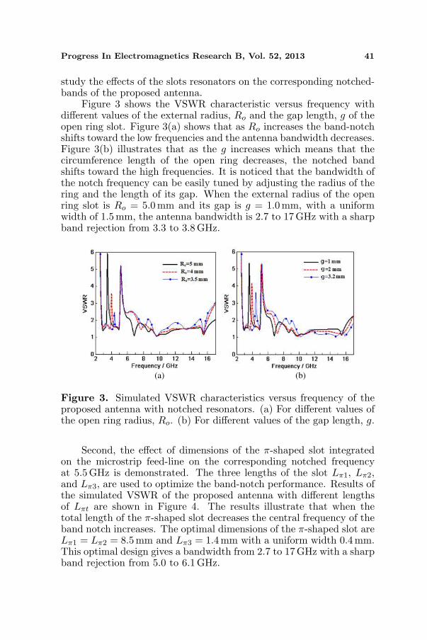
Figure 9 shows the normalized far-field radiation patterns of Eθ
and Eϕ in the y-z (E-plane) and x-z (H-plane) planes of the proposedantenna at frequencies 3.1, 4.5 and 7.5 GHz. It is observed that thesimulated patterns exhibit a relatively omnidirectional radiation in thex-zplane at these frequencies; whereas, simulated patterns in the y-zplane illustrate radiations look like E-plane radiation pattern of avertical dipole.
The simulated peak gain and the radiation efficiency of the
Progress In Electromagnetics Research B, Vol. 52, 2013 45
(a)
xz plane yz plane
(b)xz plane yz plane
(c)xz plane yz plane
Figure 9. Simulated radiation patterns of Eθ (dashed line) and Eϕ
(solid line) in the y-z and x-z planes of the proposed antenna atdifferent frequencies. (a) 3.1 GHz. (b) 4.5 GHz. (c) 7.5 GHz.
proposed antenna are shown in Figure 10. Stable gain with an averageof about 4 dBi is obtained throughout the operating band. Two sharpdips in the antenna gain can be observed in the notched-frequencybands in the vicinity of 3.55 and 5.55 GHz. This result presents thatthe proposed antenna has good dual band-notched characteristics atWiMAX and WLAN systems. The radiation efficiency is almost 75%overall the whole frequency band excluding the two rejected bands.
The proposed UWB antenna fulfills all the critical requirements

46 Ali, Saad, and Khaled
(a) (b)
Figure 10. (a) Simulated antenna peak gain, and (b) radiationefficiency versus frequencies for the proposed antenna with and withoutthe resonating slots.
including high radiation efficiency, low profile small size, stableradiation patterns and relatively constant gain. In addition, thedual notched-frequency bands at 3.3–3.8 GHz and at 5.0–6.1 GHzcan successfully block out the whole WiMAX and WLAN bands,respectively. Therefore, the potential interferences between theproposed UWB antenna and these systems can be excluded or reducedto minimum. In the other hand, the antenna bandwidth is moreenhanced in the higher frequency band, which added more benefit tothe proposed antenna to be used in other applications.
In practice, the proposed antenna is suitable to integrate withcompact UWB communication systems. As compared with thereported antennas in the literature, the proposed antenna withproximity-fed technique provides good behavior in a similar workingfrequency band with less complexity and smaller size. Table 1illustrates comparison between the behaviors of proposed antenna withthose similar designs of slot antenna configurations as given in theliterature with microstrip-fed as well as CPW-fed techniques.
5. EQUIVALENT CIRCUIT SYNTHESIZED
For further comprehension of the proposed antenna performance, aSPICE-compatible circuit modeling method is applied to the proposedantenna to establish its lumped-element equivalent circuit model.The method is described as follows: First, the response of theinput admittance/impedance of the proposed antenna obtained by

Progress In Electromagnetics Research B, Vol. 52, 2013 47
Table 1. Comparisons between the proposed antenna and the othersimilar antennas in literature.
Approach Feeding Type
Overall Size
(L X W)
(mm2)
Impedance BW
(VSWR 2)
Notched band(s), Notched Gain,
Techniques
Proposed Proximity–FED 20 X 25 2.7–17 GHz
3.3–3.8 GHz, –3.2 dBi
An Open ring slot etched off the patch
5.0–6.1 GHz, –4.5 dBi
A π–shaped slot etched off the feeding
line
Reference
[5]
CPW–FED 40 X 30 2–11 GHz
3.3–3.7 GHz, –6.5 dBi
A L–shape branch is attached to slotted
ground plane
5.15–5.825 GHz, –1 dBi
A L–shape branch is attached to slotted
ground plane
Reference
[6]
CPW–FED 39 X 35 2.6–14.34 GHz
3.3–3.7 GHz, –4 dBi
A C–shaped slot etched inside exciting
stub
5.04–6 GHz, –8dBi
A pair of open–circuit stubs
symmetrically added at the edge of the
slot
Reference
[7]
Microstrip–FED 31 X 31 2–11 GHz
3.3–4 GHz, –4.5 dBi
A pair of L–shaped slots etched on
either sides of the ground plane
5–5.7 GHz, –4.3 dBi
Modified a pair of L–shaped slots on
either side of the ground plane
Reference
[13]
Microstrip–FED 40 X 30 3.1–10.6 GHz
3.15–3.90 GHz, –10.38 dBi
A C–shaped slot etched off feeding line
5.10–5.95 GHz, –4.41 dBi
A parasitic strip is printed in circular
slot
≤
simulation or measurement is estimated in the frequency range ofinterest. There is no rule for the number of frequency points thatshould be sampled, but it is suggested to use no less than 100 points.Second, the simulated response of the input admittance/impedance isfitted by means of the Vector Fitting (VF) technique using MATLABRF Toolbox “rationalfit” to obtain a modified rational function [28].Finally, the rational function is converted into a SPICE-compatibleequivalent circuit and the synthesized component values are obtained.
The modified rational function approximation of a certainfrequency domain response F (s) using VF technique can be expressedas [29]:
F (s) =(∑N
k=1
resk
s− pk+ D
)e−s×Delay (6)
where resk and pk denote the k-th residues and poles, respectively,

48 Ali, Saad, and Khaled
which are either real quantities or come in complex conjugate pairs ofN identical sets of poles (order of approximation). s = jω representsthe complex frequency, and D and Delay are constant terms whichare real. All coefficients in Eq. (6) should be calculated so that anapproximation of F (s) is obtained over a given frequency interval. Ingeneral, VF solves this problem sequentially as a linear problem intwo stages: poles identification and residues identification, both withknown poles. The details of this procedure can be found in [30].
Without loss of generality, in this paper F (s) is applied to theadmittance-type function, Y (s), for the proposed antenna. The delayelement is always equal to zero because the presentation of the antennahas only one port [29]. The constant term Dis optional and can besynthesized with a resistance, R0 whose value is calculated as
R0 =1D
(7)
The equivalent circuit for the remaining parts of F (s) =∑N
k=1resks−pk
can be evaluated as [31].– Each real pole, F (s) = resk
s−pk, (for k = 1 to N) gives an RL-
branchLk =
1resk
, Rk = − pk
resk(8)
– Each complex conjugate pair, F (s) = res1s−p1
+ res2s−p2
, gives anRLC -branch
L =1
res1 + res2
C =res1 + res2
p1p2 +[−(p1 + p2) + res1p2+res2p1
res1+res2
]×
[res1p2+res2p1
res1+res2
]
R =1
res1 + res2×
[−(p1 + p2) +
res1p2 + res2p1
res1‘ + res2
]
R′ = − 1C
res1 + res2
res1p2 + res2p1(9)
The procedures to extract such elements can be synthesized asdescribed in [32].
The process can be started by a certain value of relative errorwhich corresponds to a certain value of N which is used as a minimumorder of approximation, say N = 2. The complete synthesis SPICE-compatible equivalent circuit for the input admittance of an antennacan provide either two real poles or one complex pair which can bemodeled as presented in Figure 11 (a pole of order N = 1 is called

Progress In Electromagnetics Research B, Vol. 52, 2013 49
(a) (b)
Figure 11. SPICE-compatible equivalent circuit for the inputadmittance of an antenna for N = 2 and D = 0. (a) For two realpoles. (b) For one complex conjugate pair.
a simple pole). Increasing the order of approximation N , will increasenumber of either resultant real poles or complex pairs.
Now use MATLAB RF Toolbox “rationalfit” to obtain a modifiedrational function. First, we compute the relative error as a vectorcontaining the dependent values of the data to be fitted. The defaulttolerance is −10 dB. If the model does not fit the original data withinthe specified tolerance, we increase the relative error-fitting tolerance,which increases the order of approximation N and increase the numberof either the resultant real poles or the complex pairs.
For instant, if the process is started with its default value relativeerror = −10 dB, the Y (s) will only fitted with six complex conjugate(N = 12) which causes the resulting approximation for Y (s) beextremely inaccurate. Consequently the root mean square errorbecomes large. For the proposed antenna the relative error-fittingtolerance after recalculation is reached to −40 dB that increase theorder of approximation to 28 and a very accurate approximation isachieved. The rational function approximation of Y (s) using VF (polesand residues) is listed in Table 2. The fitting procedure provides 14complex conjugate pairs. Figure 12 shows the magnitude and phaseerrors between the simulated results of the input admittance andthe results using “rationalfit” procedure. The figure illustrates verygood approximation and the root-mean-square error of the magnitudeis nearly 4.877e-004. Table 3 shows the components values for theequivalent circuit of the proposed antenna. The equivalent circuitmodel for the input admittance of the proposed antenna for N = 28and relative error = −40 dB is synthesized as shown in Figure 13(a).The VSWR characteristics of the proposed antenna are shown inFigure 13(b), in which very good agreement between simulated resultsand those obtained from the equivalent circuit modeling is observed.

50 Ali, Saad, and Khaled
Table 2. The rational function approximation for the inputadmittance Y (s) of the proposed antenna (when D = 0).
Type and No. of poles Poles (1e+11) Residues (1e+9)
Complex 1 –0.4231 ± 1.0943i 1.8093 ± 2.0516i
Complex 2 –0.0139 ± 0.9713i 0.0087 ± 0.0034i
Complex 3 –0.1325 ± 0.8921i 0.0608 ± 0.5051i
Complex 4 –0.0503 ± 0.7439i 0.0170 ± 0.0048i
Complex 5 –0.0392 ± 0.6377i 0.0219 ± 0.0103i
Complex 6 –0.0170 ± 0.5570i 0.0117 ± 0.0080i
Complex 7 –0.0659 ± 0.4759i 0.2793 ± 0.0193i
Complex 8 –0.0273 ± 0.4079i 0.0308 ± 0.0648i
Complex 9 –0.0294 ± 0.3533i 0.0456 ± 0.0077i
Complex 10 –0.0119 ± 0.3205i –0.0148 ± 0.0139i
Complex 11 –0.0052 ± 0.0839i 0.0430 ± 0.0156i
Complex 12 –0.0502 + 0.2423i 0.0803 ± 0.0108i
Complex 13 –0.0087 ± 0.1703i 0.0174 ± 0.0116i
Complex 14 –0.0075 ± 0.2146i –0.0095 ± 0.0006i
It is noted that the VF technique guarantees stable poles andalso enforcing passivity. With stable poles and passivity enforced, theresulting equivalent circuit may still have unphysical circuit elements(negative resistance, capacitance and inductance), as shown in Table 3,even though we use low order of approximation. But we will never getan unstable simulation since the circuit as a whole will always consumepower, whatever we connect to it [33]. However, numbers and valuesof the negative elements depend on the frequency range of the functionto be fitted as well as the order of approximation used in that fitting.Higher accuracy can be easily involved by increasing the order of theapproximation. But the complexity of the equivalent circuit will also beincreased at the same time. For instant, due to ultra-wide bandwidth,the resulting equivalent circuit may still have more negative circuitelements with large values, but the whole equivalent circuit will bepassive. A circuit having negative capacitance/inductance can present,

Progress In Electromagnetics Research B, Vol. 52, 2013 51
(a) (b)
Figure 12. Comparison of the input admittance for the proposedantenna between the simulate results and the “rationalfit” procedureresults. (a) Magnitude functions. (b) Phase angles.
Table 3. Synthesized components values for the proposed antenna.
Type andNo. of poles
L (H) R (Ω) C (F) R′(Ω)
Complex 1 2.76e–10 45.98238 1.32e–13 –92.4987Complex 2 5.75e–08 2238.108 1.60e–15 –17249.9Complex 3 8.22e–09 –5987.64 2.18e–16 6076.303Complex 4 2.94e–08 758.3636 5.71e–15 –11120.5Complex 5 2.28e–08 771.3169 8.83e–15 –4361.91Complex 6 4.28e–08 1700.955 5.14e–15 –5351.45Complex 7 1.79e–09 17.69234 2.46e–13 1234.426Complex 8 1.62e–08 –1349.12 6.82e–15 1655.607Complex 9 1.10e–08 –33.0948 7.11e–14 1580.878Complex 10 –3.37e–08 –1050.51 –1.54e–14 2256.993Complex 11 1.16e–08 41.27822 1.08e–12 –367.043Complex 12 6.22e–09 10.94282 2.69e–13 448.8052Complex 13 2.88e–08 352.2087 8.29e–14 –1148.25Complex 14 –5.26e–08 –113.187 –4.11e–14 36868.79
by duality, another inductive/capacitive element. In a negativecapacitance the current will be 180 opposite in phase to the currentin a positive capacitance. Instead of leading the voltage by 90it will lag the voltage, as in an inductor. Therefore a negative

52 Ali, Saad, and Khaled
(a) (b)
Figure 13. (a) Equivalent circuit synthesis of the proposed dualband-notched UWB antenna for N = 28 and D = 0. (b) VSWRcharacteristic as a function of frequency for the proposed antenna.
capacitance acts like an inductance in which the impedance has areverse dependence on frequency; decreasing instead of increasing actslike a real inductance. Similarly a negative inductance acts like acapacitance that has impedance which increases with frequency [34].
Finally, the major limitation of this approach is the fact that thistechnique is not systematic. In other words, the method does notcontain a physics-based approach. Nevertheless, it is stressed thatthis technique can be used as a tool to aid engineers in designingan actual passive circuit that can be used to mimic the scatteringparameter response of a UWB antenna [35]. In spite of this, goodagreement between the simulated results and the fitted data withacceptable equivalent model behaviors is obtained. The validity of themodeling method is verified, and high accurate results are achieved.The provided circuit model is useful to consider the effect of theproposed antenna when integrated with the whole communicationsystem. It also helps designers to predict the communication systemperformances.
6. CONCLUSIONS
In this paper, a miniaturized and compact UWB printed slot antennawith dual band-notched is presented. The antenna is based onmicrostrip structure with an open shunt stub, proximity-fed a circulardisk radiating patch. The proposed antenna achieves UWB conditions.It operates within a band from 2.7 to 17GHz. The proposedantenna is designed to have two band-notches to avoid the undesirable

Progress In Electromagnetics Research B, Vol. 52, 2013 53
interferences with the 3.5GHz band for WiMAX systems and the5.5GHz band for WLAN systems with a simple structure. The firstnotch is achieved by etching an open ring slot in the circular disk patch.Whereas the other notch is achieved by a π-shaped slot etched off thefeeding line. The parameters and the characteristics of the antennaare given. A detailed study of the influences of different parameterswas carried out. Curve fitting formulations are obtained to describethe influences of the notches resonators on the corresponding notchedfrequencies by using first and second order polynomial Moreover,with the help of VF technique, a SPICE-compatible lumped-elementequivalent circuit modeling for the proposed antenna is established.The proposed antenna is fabricated, and the measured data of theVSWR showed a good agreement with the simulated results alongwith the equivalent circuit modeling results. The proposed antennafeatured suitable radiation patterns with good gain flatness over theUWB frequency band excluding the two rejected bands.
REFERENCES
1. Federal Communications Commission Revision of Part 15 ofthe Commission’s Rule Regarding Ultra-Wideband TransmissionSystem, FCC, First Report and Order FCC, 02–48, 2002.
2. Khaled, E. E. M., A. A. R. Saad, and D. A. Salem, “Aproximity-fed annular slot antenna with different a band-notchmanipulations for ultra-wideband applications,” Progress InElectromagnetics Research B, Vol. 37, 289–306, 2012.
3. Dissanayake, T. and K. P. Esselle, “Prediction of the notchfrequency of slot loaded printed UWB antennas,” IEEE Trans.Antennas Propag., Vol. 55, No. 11, part: 2, 3320–3325, Nov. 2007.
4. Abbosh, M., M. E. Bialkowski, J. Mazierska, and M. V. Jacob,“A planar UWB antenna with signal rejection capability in the4–6GHz Band,” IEEE Micro. Wireless Comp. Lett., Vol. 16, No.5, 278–280, May 2006.
5. Liu, X., Y. Yin, P. Liu, J. Wang, and B. Xu, “A CPW-Feddual band-notched UWB antenna with a pair of bended dual-L-shape parasitic branches,” Progress In Electromagnetics Research,Vol. 136, 623–634, 2013.
6. Mandal, T., and S. Das, “An optimal design of CPW-fedUWB aperture antennas with WiMAX/WLAN notched bandcharacteristics,” Progress In Electromagnetics Research C, Vol. 35,161–175, 2013.
7. Li, W. M., T. Ni, S. M. Zhang, J. Huang, and Y. C. Jiao, “UWB

54 Ali, Saad, and Khaled
printed slot antenna with dual band-notched characteristic,”Progress In Electromagnetics Research Letters, Vol. 25, 143–151,2011.
8. Li, C. M., and L. H. Ye, “Improved dual band-notched UWBslot antenna with controllable notched bandwidths,” Progress InElectromagnetics Research, Vol. 115, 477–493, 2011.
9. Li, W.-M., T. Ni, T. Quan, and Y.-C. Jiao, “A compact CPW-fed UWB antenna with WiMAX-band notched characteristics,”Progress In Electromagnetics Research Letters, Vol. 26, 79–85,2011.
10. Sun, J.-Q., X.-M. Zhang, Y.-B. Yang, R. Guan, and L. Jin,“Dual band-notched ultra-wideband planar monopole antennawith M- and W-slots”, Progress In Electromagnetics ResearchLetters, Vol. 1, 1–8, 2010.
11. Tu, S., Y. C. Jiao, Y. Song, B. Yang, and X. Z. Wang, “Anovel monopole dual band-notched antenna with tapered slotfor UWB applications,” Progress In Electromagnetics ResearchLetters, Vol. 10, 49–57, 2009.
12. Zhang, J., S. W. Cheung, and T. I. Yuk, “CPW-coupled-fed elliptical monopole UWB antenna with dual-band notchedcharacteristic,” PIERS Proceedings, 823–827, Kuala Lumpur,Malaysia, March 27–30, 2012.
13. Gao, G. P., Z. L. Mei, and B. N. Li, “Novel circular slot UWBantenna With dual band-notched characteristic,” Progress InElectromagnetics Research C, Vol. 15, 49–63, 2010.
14. Yang, G., Q.-X. Chu, and T.-G. Huang, “A compact UWBantenna with sharp dual band-notched characteristics for lowerand upper WLAN band,” Progress In Electromagnetics ResearchC, Vol. 29, 135–148, 2012.
15. Mishra, S. K. and J. Mukherjee, “Compact printed dual band-notched U-shape UWB antenna,” Progress In ElectromagneticsResearch C, Vol. 27, 169–181, 2012.
16. Lui, W. J., C. H. Cheng, and H. B. Zhu, “Compact frequencynotched ultra-wideband fractal printed slot antennas,” IEEEMicro. Wireless Comp. Lett., Vol. 16, No. 4, 224–226, Apr. 2006.
17. Lui, W. J., C. H. Cheng, Y. Cheng, and H. Zhu, “Frequencynotched ultra-wideband microstrip Slot antenna with fractaltuning stub,” Electron. Lett., Vol. 41, No. 6, 294–296, Mar. 2005.
18. Karmakar, A., S. Verma, M. Pal, and R. Ghatak, “An ultrawideband monopole antenna with multiple fractal slots withdual band rejection characteristics,” Progress In Electromagnetics
Progress In Electromagnetics Research B, Vol. 52, 2013 55
Research C, Vol. 31, 185–197, 2012.19. Ali, J. K., A. J. Salim, A. I. Hammoodi, and H. Alsaedi, “An
ultra-wideband printed monopole antenna with a fractal basedreduced ground plane,” PIERS Proceedings, 613–617, Moscow,Russia, August 2012.
20. Kim, D.-O., N.-I. Jo, D.-M. Choi, and C.-Y. Kim, “Design ofthe ultra-wideband antenna with 5.2 GHz/5.8 GHz band rejectionusing rectangular split-ring resonators (SRRS) loading,” Journalof Electromagnetic Waves and Applications, Vol. 23, No. 17–18,2503–2512, 2009.
21. Kim, J., C. S. Cho, and J. W. Lee, “5.2 GHz notched ultra-wideband antenna using slot-type SRR,” Electron. Lett., Vol. 42,315–316, 2006.
22. Liu, L., Y. Z. Yin, C. Jie, J. P. Xiong, and Z. Cui, “A compactprinted antenna using slot-type CSRR for 5.2GHz/5.8GHz band-notched UWB application,” Microw. Opt. Techn. Lett., Vol. 50,3239–3242, 2008.
23. Yin, X. C., C. L. Ruan, C. Y. Ding, and J. H. Chu,“A compact ultra-wideband microstrip antenna with multiplenotches,” Progress In Electromagnetics Research, Vol. 84, 321–332, 2008.
24. Lai, H.-Y., Z.-Y. Lei, Y.-J. Xie, G.-L. Ning, and K. Yang, “UWBantenna with dual band rejection for WLAN/WiMAX bands usingCSRRs,” Progress In Electromagnetics Research Letters, Vol. 26,69–78, 2011.
25. Zhang, Y., W. Hong, C. Yu, Z.-Q. Kuai, Y.-D. Don, and J.-Y. Zhou, “Planar ultrawideband antennas with multiple notchedbands based on etched slots on the patch and/or split ringresonators on the feed line,” IEEE Trans. Antennas Propag.,Vol. 56, No. 9, 3063–3068, Sept. 2008.
26. Xu, F., Z. X. Wang, X. Chen, and X.-A. Wang, “Dual band-notched UWB antenna based on spiral electromagnetic-bandgapstructure,” Progress In Electromagnetics Research B, Vol. 39, 393–409, 2012.
27. Saad, A. A. R., D. A. Salem, and E. E. M. Khaled, “5.5 GHznotched ultra-wideband printed monopole antenna characterizedby electromagnetic band gap structures,” International Journalof Electronics and Communication Engineering (IJECE), Vol. 1,No. 1, 1–12, Aug. 2012.
28. MATLAB Program, The MathWorksTM, Inc., Version 7.10.0.499(R2010a), Feb. 2010.

56 Ali, Saad, and Khaled
29. Zeng, R. and J. Sinsky, “Modified rational function modelingtechnique for high speed circuits,” IEEE MTT-S Inter. Microw.Symp. Digest, 1951–1954, San Francisco, Jun. 2006.
30. Gustavsen, B. and A. Semlyen, “Rational approximation offrequency domain responses by vector fitting,” IEEE Trans. PowerDelivery, Vol.14, 1052–1061, Jul. 1999.
31. Ren, W., “A new circuit modeling methodology for RFIDantennas with vector fitting technique,” 6th Intern. Conf. WirelessComm. Networking and Mobile Computing (WiCOM), 1–4,Chengdu, China, Sept. 2010.
32. Antonini, G., “SPICE equivalent circuits of frequency-domainresponses,” IEEE Trans. Electrom. Compatibility, Vol. 45, No. 3,502–512, Aug. 2003.
33. Gustavsen, B. and A. Semlyen, “Enforcing passivity foradmittance matrices approximated by rational functions,” IEEETrans. Power System, Vol. 16, 97–104, Feb. 2001.
34. Hickman, I., Analog Circuits Cookbook, 2nd Edition, Newnes, NewYork, 1999.
35. DeJean, G. R. and M. M. Tentzeris, “The application of lumpedelement equivalent circuits approach to the design of single-portmicrostrip antennas,” IEEE Trans. Antennas Propag., Vol. 55,No. 9, 2472–2468, Sept. 2007.


![Printed Egg Curved Slot Antennas for Wideband Applications · wide-slot antenna fed by a microstrip line with a rotated slot for bandwidth enhancement is proposed in [1] with operating](https://img.dokumen.tips/doc/110x75/5fd1ea513ac4222b78003805/printed-egg-curved-slot-antennas-for-wideband-wide-slot-antenna-fed-by-a-microstrip.jpg)


![Miniaturized Triple Wideband CPW-Fed Patch Antenna With a ... · Double L-slot microstrip patch antenna array for WiMAX and WLAN applications is proposed in [20]. A coplanar waveguide](https://img.dokumen.tips/doc/110x75/5f14d7603b24ad1cb956d521/miniaturized-triple-wideband-cpw-fed-patch-antenna-with-a-double-l-slot-microstrip.jpg)