Embed Size (px)
Citation preview

A CONTINUOUS MODEL FOR THE TAPPED-INDUCTOR BOOST CONVERTER
R. D. Middlebrook
Cal i fornia Inst i tute of Technology Pasadena, Cal i fornia 91125
ABSTRACT
A continuous, 1ow-frequency, smal l -s ignal averaged model for the tapped-inductor boost converter with input f i l t e r i s developed and experimentally ver i f ied , from which the dc transfer function and the smal l -s ignal l ine input and duty rat io input describing functions can eas i ly be derived. A new effect due to storage-time modulation in the t ransistor switch is shown to explain observed excess f i l t e r damping resistance without associated loss in conversion ef f ic iency. The presence of an input f i l t e r can cause a severe disturbance, even a n u l l , in the control duty rat io describing function, with consequent potential performance d i f f i c u l t i e s in a converter regulator.
1. INTRODUCTION
A method of modeling switching converter transfer functions has been described by Wester and Middlebrook [1 ] , and applied to the basic buck, boost, and buck-boost converters in the continuous conduction mode. The principle is to replace the several d i f ferent , lumped, l inear models that apply in successive phases of the switching cycle by a s ingle lumped, l inear model whose element values are appropriate averages over a complete cycle of their successive values within the cycle. The result ing "averaged" model permits both the input-to-output ("line") and duty rat io-to-output ("control") transfer functions to be eas i ly obtained for both dc (steady state) and superimposed ac (describing function) inputs. The nature of the model derivation inherently res t r ic ts the va l id i ty to frequencies below the switching frequency, and model l inear i ty is ensured by independent restr ic t ion of the superimposed ac signal to small amplitudes. The result i s therefore a s m a l l - s i g n a l , low-frequency, averaged model.
The models obtained in [1] show that the l ine and control describing functions contain the anticipated low-pass LC f i l t e r response characterized by a pair of le f t half-plane poles and, i f there is nonzero resistance in ser ies with the capacitor, by a le f t half-plane real
zero. The pole-pair posit ions are conveniently ident i f ied in terms of the f i l t e r corner f requency and peaking factor , or Q-factor. Two results of part icular s igni f icance for the boost and buck-boost converters are that the f i l t e r corner frequency and Q-factor both vary with steady-state duty rat io D and, even more important, that the control describing function acquires a r ight half-plane real zero.
Several extensions and developments of the results of [1] are presented in th is paper.
1. A s m a l l - s i g n a l , low-frequency, averaged model i s derived for the tapped-inductor converter, of which the or ig inal ("simple") boost converter i s a special case.
At the same time, the c i rcu i t being modeled i s extended to include the l ine input f i l t e r that i s almost invariably present in a practical system, and the modeling process i s refined to include a more accurate representation of the c i rcu i t losses that affect the Q-factor. The motivation for the modeling refinement was to explain measured Q-factors that were s i g n i f i cantly lower than predicted by the or iginal model even when the most generous values for the physical loss- res is tances were allowed. However, although the refined model did indeed predict lower Q-factors, the quantitative effect was s t i l l insuf f ic ient to explain the observed d i s crepancies.
I t turned out that a quite different effect was responsible for the lower Q-factor, namely, modulation of the storage time of the t rans is tor switch. The physical cause-and-effect sequence i s as fol lows: an applied smal l -s ignal ac modulation of the switch duty rat io causes a corresponding modulation of the current carried by the switch at the instant of turn-off , and a consequent modulation of the storage time. The resul t i s that the actual switch output duty rat io modulation amplitude i s dif ferent from the switch drive modulation amplitude. I t may seem surpr is ing at f i r s t s ight that th is effect would cause only a lowering of the Q-factor , without affecting any of the other qual i tat ive or quantitative features of the model;
PESC 75 RECORD—63

nevertheless, this i s indeed confirmed by the other principal extension presented in this paper:
2. A storage-time modulation effect in the switch i s shown to result in an effective series resistance in the s m a l l - s i g n a l , low-frequency, averaged model of the tapped-inductor boost converter, whose presence lowers the apparent Q-factor of the low-pass f i l t e r character ist ic contained in both the l ine and control describing functions.
Experimental resul ts are presented for various conditions chosen s p e c i f i c a l l y to expose the functional dependence of the model element values upon the several parameters, in order to maximize the degree of model ver i f icat ion thereby obtained. In addition to such quantitative v e r i f i c a t i o n , the following general conclusions are of part icular interest :
1. The effective series resistance RM in the model due to t rans is tor switch storage-time modulation lowers the f i l t e r Q-factor, but i t does not lower the conversion ef f ic iency; in other words i t i s only an apparent resistance and not an actual loss resistance.
2. The presence of an LC input f i l t e r can cause a serious modification of the control describing function. A dip in the magnitude of the control describing function can occur in the neighborhood of the resonant frequency of the input LC f i l t e r . This dip is characterized by a complex pair of zeros in the control describing function. As the steady-state duty rat io i s increased, as happens in normal regulation adjustment of a closed-loop converter system, the complex pair of zeros cannot only reach the imaginary axis of the complex frequency plane, causing the dip in the magnitude response to become a n u l l , but can move into the r ight half-plane causing a large amount of additional phase l a g . A possible null in the control describing function magnitude response of course could severely degrade the performance, and the excessive phase lag could ser iously affect the s t a b i l i t y , of a closed-loop regulator system. The model presented here is useful in both the qual i tat ive and quantitative design of such a system to guard against such disastrous eventual i t ies .
2. DEVELOPMENT OF THE CONTINUOUS MODEL
The elements of a tapped-inductor boost converter are shown in F ig . 1. An input f i l t e r , which would invariably be used in a practical system, is included between the supply voltage V q
and the input of the converter i t s e l f . As far as the operation of the converter i s concerned,
and C s need be only the f i l t e r elements L s , R S , e x p l i c i t l y represented; the box around~the L $ is to imply that additional input f i l t e r elements may be present without affecting the nature of the converter operation. The resistances R § and R C
in F ig . 1 are always present in a practical c i rcu i t even i f they represent only capacitance esr .
Some waveforms in the c i rcu i t of F ig . 1 under steady state operation are shown in Fig. 2. The t rans is tor switch i s closed for a fraction
Ν turns
Fig, 1 . C i rcu i t of the tapped-inductor boost converter with input f i l t e r .
DT S
I _ amp-turns * ' Ν
( l -D)T s = D , T s
Fig . 2. Some waveforms in the c i rcu i t of F ig. 1: v s , i £ , and ν are continuous; ν i s quasi-continuous; i s i s discontinuous.
64—PESC 75 RECORD

T SD of i t s period T s = l / f s , where f s i s the switching frequency, and i s open for the remaining fraction T S D ' = T s ( l - D ) . While the switch i s closed, the current i s in the fraction N/n x of the total inductor turns Ν ramps up as energy is stored in the inductor; part of i s i s supplied from the input by i g , and the balance comes from discharge of C s causing a f a l l in the capacitance voltage v s . At the same time, the diode is open and the capacitance C d i s charges into the load R causing a fa l l in the voltage v c . While the switch i s open, the diode i s closed and the current i s in the total inductor turns Ν ramps down as the stored inductor energy discharges into the load and recharges C, causing a r ise in v c . Since i^ drops below i q , C s i s recharged causing a r ise in the voltage v s .
Boundary conditions l inking the waveforms in the two intervals depend upon the requirements that capacitance voltages and inductor ampere-turns cannot change instantaneously at the switching ins tants . Consequently, the voltages v $ and v c are continuous at the switching ins tants , whereas the output voltage ν has steps at the switching instants because of the drop in R c . S i m i l a r l y , the inductor ampere-turns i s continuous at the switching ins tants , and i t is convenient to i l l u s t r a t e this in terms of a quantity i Ä defined as "ampere-turns per turn," a lso shown in F i g . 2. Thus, i £ i s continuous but the actual inductor current i s has steps of rat io n x at the switching instants . Ident i f icat ion of i n i s an important step in the derivation of the continuous model.
Waveforms shown in F ig . 2 are for the "continuous conduction" mode of operation in which the instantaneous inductor current does not f a l l to zero at any point in the cycle , and the entire discussion and results of th is paper apply only to th is mode. Average, or dc, values of the waveforms are also shown in F ig . 2. The dc output voltage V is of course equal to the dc voltage V c on capacitance C.
A suitable equivalent of the c i rcu i t of F ig. 1 from which to begin derivation of the averaged model i s shown in Fi g. 3, and includes
F ig . 3. Switched model equivalent to the c i rcu i t of F ig. 1 ; s tar t ing point for derivation of the continuous model of F ig . 10.
several paras i t ic resistances of obvious physical or ig in which are important in determining the effective Q of the impl ic i t f i l t e r response character is t ic . There are two independent "driving" s i g n a l s : the l ine voltage V g and the duty rat io d. Each i s taken to have a dc part and smal l -s ignal ac part , so that Vg = V g + v g and d = D + d. Since the "complementary" duty rat io 1-d frequently occurs in the equations, i t i s given the symbol d' = 1-d, so that d' = 1-D-d = D ' - d . As a consequence of the dc and ac components of the two driving s i g n a l s , a l l other voltages and currents in the c i rcu i t also have dc and ac components, in part icular the output voltage ν = V + v. The analysis objective i s to f ind a continuous model (unlike the switched model of F ig . 3) from which the dcand ac components of the output voltage V and ν can be found from the dc and ac components of the two driving s igna ls V g , v g and D, ά.
The approach taken i s an extension of that in [1 ] , in which the smal l -s ignal ac components V g , a , etc. are taken to be slow compared with the switching frequency f s . This rest r ic t ion permits the nonlinear model of F ig . 3, which consists of two switched l inear models, to be approximated by a l inear model whose element values are appropriate averages of their values in the two intervals T s d and T - d ' . Furthermore, th is approach permits most of the analysis to be performed through successive transformations and reductions of c i rcu i t models; physical ins ight i s thus better retained, and understanding made eas ier , than i f analysis i s performed ent irely by algebraic manipulation. The resul t of this approach i s an "averaged" model from which the two transmission charact e r i s t i c s can be obtained for dc and for ac at frequencies below the switching frequency.
The objective i s to combine the two separate l inear models of the piecewise-l inear model of F ig . 3 into a s ing le l inear model. The procedure consists of a number of steps in manipulation of the model, which wi l l be presented here for a s l i g h t l y s impl i f ied version of F ig . 3 in which R $ , R w , R v , Rj,and R ç are set equal to zero. This i s done so that the method may be i l lus t ra ted without the burden of extra elements and terms which merely complicate the diagrams and equations. The effects due to these temporarily discarded elements w i l l , however, be restored into the f inal resu l ts . A l s o , a number of comments concerned with the s igni f icance and interpretation of certain steps wi l l be deferred unti l the end of the der ivat ion.
Step 1 . Draw separately the l inear models of F ig . 3 that apply during each of the intervals T s d , T $ d ' as shown in F i g s . 4(a) and 4(b) respectively. Identify the voltages and currents that are continuous across the switching ins tan ts , namely the capacitance voltages v s , v c , and the ampere-turns per turn of both the switched inductor, i £ , and the input f i l t e r inductor, i Q .
PESC 75 RECORD—65

φ
Cs
R u n x i , L/ηχ
(α) interval T s d
same topology i f the rat io i s 0:1 in Fig. 5(a) and 1:1 in F ig . 5(b) .
Step 3. Replace the ideal transformers in F ig . 5 by ideal dependent generators whose control l ing s igna ls are voltages or currents that are continuous across the switching instants . This i s done in Fig. 6. (Notation: squares are used to represent dependent generators, c i rc les represent independent generators.)
Cs Φ
(b) interval T s d ' = T 8 ( l -d)
Fig . 4. Step 1 in the model derivation (paras i t ic resistances in model of F ig . 3 omitted): separate l inear models that apply during the two intervals Τ d and Τ d ' . 3 s s
Step 2. Manipulate the models of F ig . 4 to have both the same topology and the same values of the continuous voltages and currents at corresponding po in ts , as shown in F ig . 5. In the present case, th is requires scal ing of the current n x i n in F ig . 4(a) to match the current i Ä in F ig . 4 (b) , which i s done by introduction of an ideal transformer of rat io l : n x in F ig . 5 (a ) ; since the voltage v s i s already the same in both models, the transformer i s introduced to the r ight of C s . To produce the same topology, a 1:1 transformer i s introduced in the same place in F ig . 5(b) . A l s o , since the current i Ä flows into C during interval T s d ' but does not during interval T s d , introduction of another ideal transformer to the le f t of C allows th is condition to be realized with the
nx.,mmnxvs
(a) interval T,d
(b) interval T sd'
Fig. 6. Step 3: replacement of ideal t ransformer by dependent generators controlled by continuous var iables.
Step 4. Coalesce the two topological ly identical models of F i g s . 6(a) and 6(b) into a s ingle model in which the various s igna ls have the average of their values throughout the entire period T s , as shown in F ig . 7. For
(dn?+d')R u
1% ^ r :
V c
c1
Ο: I Fig. 7. Step 4: coalesced models for the
two intervals into a s ingle averaged model; implies imposition of the low-frequency res t r ic t ion .
(b) interval T s d'
Fig . 5. Step 2 : introduction of ideal transformers to establ ish the same topology and to expose the same continuous variables for the two interva ls .
example, the dependent current generator which has a value n x i ^ for an interval T s d and a value i£ for an interval T s d ' has an average value ( d n x + d ' ) i £ over the entire period T s , and s imi la r ly for the other dependent generators. The pair on the r i g h t , of course, constitutes a special case in which the signal i s zero for one of the intervals . The coalescing process takes a s l i g h t l y different form for an element whose value i s not the same in the two in terva ls : the resistance ( d n x
2 + d ' ) R u in F ig. 7 i s the value
66—PESC 75 RECORD

having a voltage drop across i t equal to the average of the voltage drops in the two intervals T s d and T $ d ' .
Step 5. Substitute dc and ac components for the variables in F ig . 7. For example, the left-hand dependent current generator i s expressed as:
( d n x + d ' ) i £ = [ ( D + u ) n x + ( D ' - d ) ] ( I ^ i Ä )
= ( D n x + D ' ) ( I Ä + i Ä ) + ( n x - l ) I £ d + ( n x - l ) i Ä d
% ( D n x + D ' ) i £ + ( n x - l ) I £ d
The approximation of the f inal l ine i s neglect of the ac product term, which i s val id for small ac s igna ls superimposed on the dc. This generator, therefore, may be decomposed into a dependent generator proportional to i £ , and an independent generator proportional to the driving signal d, as shown in Fig. 8. This figure shows
( N 2 - i ) R u i , d |_ V c ;
Fig. 8. Step 5: substi tut ion of dc and ac components; implies imposition of the smal l -signal res t r ic t ion .
corresponding manipulations of the other three dependent generators of F ig . 7. The subst i tut ion process for the averaged resistance is as fol lows. The voltage across ( d n x
2 + d ' ) R u i s
<dV+ d'>RuV [(D+dJnZ+iD'-cD^d^^)
where again the product term in i^d is omitted. This voltage can be represented as that across a resistance plus an independent generator proportional to 3 , as shown in F ig . 8. For conciseness, the factor ΰη χ+ϋ' i s replaced by ϋ χ .
Step 6. Replace the dependent generators by corresponding ideal transformers, and add a resistance R M to the le f t of the D x transformer, as shown in P ig . 9. To compensate for th is addit ion, the reflected value D X
2 R U must be subtracted from the right-hand side of the D x
transformer so that the net resistance in th is branch i s then [ (Dn x
2 +D' ) - D x
2 ] R g , which reduces to D D ' ( n x - l ; 2 R u as shown in F ig . 9. One other change has been made in F ig . 9, namely the independent generator I £ d has been reflected from the r ight to the le f t side of the D' transformer.
R u
Φ . {nx-\)lxd
DD'(nx-l) R u ( η , - D R ^ d
• - - F + H +
(n x - l )V s d L u
Vcd
| : D X D': I
Fig . 9. Step 6: Restoration of ideal t ransformers in place of the dependent generators and adjustment of certain element pos i t ions .
As mentioned at the beginning of the der ivat ion, the resistances R s , R w , R y , R d ,and R c were omitted. I f these elements are included, the model of F ig . 9 becomes extended to that shown in F ig . 10, in which
è 3 . [ ( D - D - ) ( n x - l ) 2 R s - ( n x
2 - l ) R u
- ( " x V V - D ' ( R
CH R ) ] I * d
( D
(2)
(3)
(4)
(5)
RT = D D ' ( n x - l ) [ ( n x - l ) ( R S + R u ) ] + n X R W - R V ] (6)
R 2 E D D ' ( R D + R C | | R ) (7)
D n x R w + D / R v
Dn x + D' Λ
I : D x D': I Fig. 10. Continuous, dc and low-frequency
smal l -s ignal ac,averaged model for the tapped-inductor boost converter of F ig . 3 (paras i t ic resistances restored); D and d refer to duty rat io at the t rans is tor c o l lector.
The c i rcu i t of F ig . 10 is the complete continuous model of the tapped-inductor boost converter, including input f i l t e r , from which the dc and ac l ine and control transfer functions can eas i ly be obtained.
PESC 75 RECORD—67

The ideal transformers operate down to dc, and the dc output voltage V i s obtained as a function of V q and D by solution with the ac generators set equal to zero. Actua l ly , to allow for an unspecified input f i l t e r , i t i s more convenient to solve for the dc output voltage V as a function of D and of the dc voltage at the input f i l t e r output, which i s the same as the input f i l t e r capacitance voltage V $ . The dc component I £ of the inductor ampere-turns per turn current i s
D V χ χ
D , 2 R + R T
(8)
where
R T Ξ D x 2 [ R u + ( D n x R w + D , R v ) / D x ] + R l + R 2 + D ' 2 R d ( 9 )
i s the total effective resistance referred to the middle loop in F ig . 10. The dc output voltage i s then
1 V = D ' I R = - 4
D 1 + Rj/D R (10)
This equation represents the basic boost property of the converter; for a high-ef f ic iency system, the effective dc loss resistance Rj i s small compared with the reflected load r e s i s tance D , 2 R , so V ^ ( D X / D ' ) V S . For reduction to the simple boost converter, n x = 1 so D x = Dn x+D' = 1 , and then V % ( 1 / D ' ) V S .
The l ine describing function i s obtained from the model of F ig . 10 by solut ion for v / V g , and the control describing function i s obtained as ν /α through use of the generators ê ] , e 2 > eg , j i , and each of which i s proportional to d. Before consideration of such appl icat ions of the model, however, some comments wi l l be made concerning i t s form and derivat ion.
The essence of the procedure of the model derivation i s contained in step 4, in which the two models of F ig . 6 for the intervals T $ d and T s d ' are coalesced into a s ingle model. The exact average of the two current generators, n x i £ from F ig . 6(a) and i £ from Fig . 6 (b ) , i s < d n x i £ + d ' i £ ) . An essential approximation i s then made in the replacement of the average of the product of two variables by the product of their averages, so that <dn x i£ + d ' i n ) = <dn x i ,> + y < d ' i A > %<d>n x <i Ä > + < d ' ) < i \ > = (<d)n x + < d ' ) ) < i Ä > . I t i s this f inal form that i s shown against the left-hand dependent current generator in F ig . 7 , except that for s impl ic i ty in notation the averaging signs { ) have been omitted. As described in [1] , the above approximation i s va l id i f at least one of the variables i s continuous; in th is case, d i s not continuous ( i t changes from 1 to 0 ) , but i*£ is continuous. As also discussed in [1] , the averaging process imposes an upper frequency l imi t on the va l id i ty of the resu l t , and i t i s for this reason that the model of F ig . 10
i s a low-frequency averaged model, val id for ac signal frequencies much lower than the switching frequency.
The steps leading up to step 4 have the purpose not only of molding the separate l inear models for the two switching intervals into s imi lar topological forms, but also of sett ing up the quantit ies that are to be averaged in such a way that the current or voltage factor in the product is one that i s continuous across the switching instants . Thus, in F i g s . 6 and 7 , the quantit ies to be averaged a l l contain i 'o, ν , or v c (ac tua l ly , the state variables of the system) as one of the fac tors , and the inductor ampere-turns per turn i £ was s p e c i f i ca l ly ident i f ied for this purpose. In contrast , the actual inductor current i $ and the output voltage v, for example, are not continuous across the switching ins tants , as seen in F ig . 2, and their use i s therefore suppressed in the manipulations leading up to step 4, although the detai ls were not exp l ic i t because of omission of the various paras i t ic resistances.
In the f inal result of F ig . 10, a l l the paras i t ic resistances R $ , R w , R v , R u , R c , and a lso R u which was retained throughout the derivat i o n , appear in the same physical posit ions as in the or ig inal c i rcu i t of F i g . 3. (Although since R w and R y each appears in the or ig inal model for only one of the two switching in te rva ls , they appear in Fig. 10 in an appropriately averaged form with an obvious physical interpretat ion. I t i s for this reason that these averaged forms are purposely inserted in the shown posit ion in Fiq. 10, just as R(j in the adjacent posit ion was purposely added in step 6.)
In addition to the appearance of the paras i t ic resistances in the expected p laces, the model of F ig . 10 shows the presence of two additional resistances R] and R2 defined by Eqs. (6) and (7), which are related to the paras i t ic resistances. I t i s interesting to note that R-j and Rj are zero at both zero and unity dc duty rat io (D = 0 and D' = 0 ) , and have maximum values at D = D' = 0.5. The additional resistances R-j and R2 appear in the averaged model of F ig . 10 because of s t r i c t adherence in the derivation to the requirement that one of the two quantit ies in an averaged product must be continuous across the switching instant . However, as seen in the waveforms of F ig . 2, the output voltage v, for example, while not continuous may be considered quasi-continuous in that the steps are small compared to the total value. I f quasi-continuity i s accepted instead of s t r i c t continuity in step 4 of the der ivat ion, then the resistances R-j and R2 do not appear in the resul t . This s impl i f ied procedure was followed in [1] in the derivation of an averaged model for the simple boost converter.
To see the s igni f icance of the "extra" resistances R-j and Rp, consider the model of F i g . 10 reduced for determination of the l ine describing function v / V g . For this case of
68—PESC 75 RECORD

constant duty ra t io , the ê 's and j ' s are a i l zero, and for further s impl ic i ty let the input f i l t e r be omitted. Then, with the two t ransformers eliminated by appropriate ref lect ion of the elements in the outer loops into the center loop, the result ing reduced model i s as shown in F ig . 1 1 . The l ine describing function v / V g is simply that of a lossy LC
Rr D'v
D£R U D x (Dn x R w +D'R v ) R, R2 D' R d
φ OS
D Rc:
_c_. r v 2 '
Fig. 1 1 . Reduced version of averaged model of F ig . 1 0 for determination of the l ine describing function v / v g , without input f i l t e r ; R T i s the total effective series resistance.
f i l t e r whose Q-factor is determined (in part) by the total effective series resistance R j , defined in Eq. ( 9 ) and in F ig . 11 as the sum of the various paras i t ic resistance elements shown. Clear ly , R-j and Ro increase the effective loss and lower the Q.
spite of the constant duty rat io base drive. Since the t rans is tor col lector turn-off i s delayed after the base turn-off drive by the storage time, a possible explanation of the effect i s that the storage time is being modulated by the l ine ac s i g n a l . This could occur because the l ine ac signal modulates the current carried by the t rans is tor during the on-time, and the storage time i s dependent upon the col lector current to be turned of f .
In an attempt to establ ish a quantitative model of th is e f fect , an obvious s tar t ing point is an expression for storage time t s as a function of the col lector current Iç to be turned of f , and of the base drive condit ions. From well-known charge-control considerat ions, such an expression i s [2]
T S M1 ΣΒ2 + ^ 1
i J — n ^ j ( Π )
in which τ i s the base carr ier l i fet ime in the saturated on" condit ion, Iß] i s the forward base current jus t before turn-of f , Iߣ i s the turn-off (reverse) base dr ive , and 3 i s the active current gain for the col lector current I q at the end of the storage time. For typical turn-off overdrive such that Iß2 >> I c / 3 9 the log may be expanded to give
The or iginal motivation for the model derivation including s t r i c t continuity of one of the variables in an averaged product, which leads to the appearance of R] and Ro, was to explain measured Q factors in both the l ine and control describing functions that were s ign i f i can t ly smaller than those predicted in the absence of R] and Ro. However, although the improved model provided a qual i tat ive change in the r ight d i rect ion, the quantitative lowering of the Q caused by the addition R-j and Ro was insuf f ic ient to explain the observed resu l ts . An entirely different effect, discussed in the next sect ion, was found to be the cause of the observed low Q.
3 . MODEL EXTENSION FOR STORAGE TIME MODULATION EFFECT
When a measurement of the ac l ine describing function is made in the tapped-inductor boosf converter shown in F ig . 1 , an ac variat ion v g i s superimposed on the l ine voltage V g and the t ransis tor switch i s driven from a modulator in such a way that the base drive i s turned on and off with constant (dc) duty ra t io , without any control signal ac modulation. As described above, such measurements showed a Q-factor s i g n i f i c a n t l y lower than could be accounted for by reasonable values of known paras i t ic loss resistance.
However, in the course of such measurements, i t was noted that the t ransis tor switch duty rat io at the col lector was in fact being modulated by the injected l ine ac s i g n a l , in
t ^ t s so 31 B2 where
so x s *n ( l + I B 1 / I B 2 )
(12)
( 1 3 )
Hence, for constant base turn-on and turn-of f drive currents, the storage time decreases l inear ly with increasing lQ to be turned off .
The next step i s to incorporate this result into the duty rat io re lat ionship. I f the base is driven with duty rat io d B so that the on-drive is present for an interval T s d B of the switching period T s , then the col lector wi l l remain "on" for an interval T s d given by
V • V b + * s so that
where
d B + T
3 l B 2 T s
SO
M
( 1 4 )
( 1 5 )
( 1 6 )
i s a "modulation parameter" that describes how the col lector duty rat io d in Eq. ( 1 5 ) i s affected by the col lector current I q .
In the context of the tapped-inductor boost converter of F ig . 1 , the col lector current to be turned off i s the inductor current in the interval T s d , namely i s = n „ i £ (F ig . 2 ) . In general, the base drive duty rat io d B has dc and smal l -s ignal ac components dg = Dg + âo that contribute to the corresponding components = I £ + i Ä , so that ,
PESC 75 RECORD—69

from Eq. (15),
d = D so M
d B " I M (17)
The dc and smal l -s ignal ac terms in the above equation represent respectively the dc and smal l -s ignal ac col lector duty rat ios D and α that were employed in the development of the continuous model of F ig . 10. Al l that i s necessary, therefore, to account for the col lector storage time modulation effect i s to substi tute the above expressions wherever D and α occur in the model of F ig. 10 and the associated equations (1) through (7) . The dc subst i tut ion represents merely a small of fset in the dc duty r a t i o , and i s of no qual i tat ive concern. In the ac subst i tu t ion , the term of importance i s that in i £ , so that the f ive ê and 3 generators of F ig . 10 and Eqs. (1) through (5) each gains an additional generator as shown e x p l i c i t l y in F ig. 12, in which
^Ml
RM2 ~ V c ^ M
(18)
(19)
^M3 n x [ ( D - D ' ) ( n x - l ) 2 R s - ( " x 2 - l ) R u
K W - d - (R c | | R ) 3 I A / I „ (20)
— I / I D' r M
( 2 1 )
( 2 2 )
i. |K, i
êi e3 ê 2 / Λ
I ö Φ.
Fig . 12. Extension of model of F ig . 10 to include generators that represent the t ransis tor storage-time modulation ef fect .
In F ig . 12, the e and j generators are s t i l l given by Eqs. (1) through (5 ) , with άβ s u b s t i tuted for ά. However, now that the col lector storage modulation effect has been exp l ic i t l y accounted for in the model, i t i s more convenient merely to drop the sub Β and to redefine D and α to refer to the base drive duty rat io rather than to the col lector duty ra t io , so that the small difference between D and D ß
i s impl ic i t ly ignored and Eqs. (1) through (5) remain applicable as they stand.
Some further manipulation of F ig . 12 leads to a simpler and more useful model. F i r s t , i t i s noted from Eq. (17) that η χ Ι £ / Ι Μ
represents the difference between the col lector and base dc duty rat ios due to the influence of the col lector dc current η χ Ι ^ upon the storage time. For normal designs this difference wi l l be suf f ic ient ly small that η χ Ι ^ / Ι Μ << 1. I t then follows from Eqs. (21) and (22) that K-j << 1 and K2 << 1 , except perhaps for extreme conditions where η χ >> 1 (very low inductor tap r a t i o ) , or D 1 << 1 (approaching unity duty rat io D). In F ig . 12, the ac current K-jî i s summed with the ac current D x i £ at point A ] , and the current K 2 ? £ i s summed with at point A 2 ; therefore, to the extent that Κ ] , K2 << 1 both the K-j and the K? generators in F ig . 12 have negl ig ib le effect and can be omitted from the model.
Second, i t i s seen that each of the R^ dependent generators in F ig . 12 i s proportional to the ac current flowing through i t , and can therefore be direct ly replaced by the corresponding resistance.
The result ing model i s shown in Fig. 13, in which^the K-j and K2 generators are dropped and the e generators and R^ resistances are condensed to
e = θ ί + e 2 + e 3
RM = RM1 + RM2 + RM3
(23)
(24)
Some reduction and s impl i f icat ion in these expressions can be achieved by comparison of the contributing terms. From Eq. (10), V c = V = D ' I Ä R and i t can then be seen fron^Eqs. (2 ) , (3) and (19), (20) that the rat ios e 3 /e2 and RM3^RM2 are. on the order of the rat io between
DrixRw+D'Rv RMI + RM2+RM3 v \Dn x +D'
Φΐ
A I,+î,
Φ,
D x = Drix+D'
I : D x D':l
Fig. 13. Complete continuous, dc and low-frequency smal l -s ignal ac , averaged model for the tapped-inductor boost converter of F ig . 3, including the "modulation resistance" RM which i s present only in the ac model; D and 3 refer to duty rat io at the t ransistor base.
some combination of the paras i t ic resistances and the load resistance R; consequently, the contributions êo and R M 3 can be dropped in Eqs. (23) and (24). Then, from Eq. (10) with a s imi lar degree of approximation, V = ( D X / D ' ) V S and the remaining terms in Eqs. (23) and (24) can be combined to give
70—PESC 75 RECORD

3 l B 2 T s The f inal model i s a continuous, averaged
model for the tapped-inductor boost converter with input f i l t e r , including the t ransis tor switch storage-time modulation effect accounted for by the resistance R m . I t i s va l id for both dc and smal l -s ignal ac with the proviso that the resistance R ^ i s to be included only in the ac model and not in the dc model. This is necessary because of the step by which the model of F ig . 13 was obtained from that of Fig. 12: the total current through the R M
generators of F ig . 12 i s l £ + 1 \ » but t h e
generators^are functions only of the ac component î . In the f inal model of F ig. 13, the resistance R ^ i s enclosed in an oval as a reminder that i t i s to be included only in the ac model.
I t i s seen from Fig . 13 that inclusion of the storage-time modulation effect leads to a modification in the model that i s at least potential ly capable of explaining the observed properties: the appearance of the ac resistance Rjvj lowers the Q of the impl ic i t f i l t e r character is t ic , and the fact that the effect i s represented only by a resistance confirms that no other property of the model is affected.
The storage-time modulation effect i s manifested through two parameters: f i r s t , the parameter Ijvj defined in Eq. (16) i s determined by t rans is tor internal properties T s and e , and by the switch input c i rcu i t drive conditions described by the period T s and the turn-off base current Iß2> second, the parameter RM which, by Eqs. (18) through (20) and (23), i s inversely proportional to I j and is a function also of the switch output c i r c u i t , namely the boost converter element values and operating condit ions.
4. MODEL REDUCTION AND EXPERIMENTAL VERIFICATION
Although the qual i tat ive nature of the dc character ist ic V as a function of Vg and D and of the ac l ine describing function v / V g are obvious from the model of F ig. 13, the^nature of the ac control describing function ν / α is not so obvious because the driving signal^enters through the three separate generators ê , and J 2 - Understanding and interpretation of this character ist ic is therefore fac i l i t a ted by some further manipulation and reduction of the c i rcu i t of F ig . 13 for some special cases.
I f the input f i l t e r i s omitted, the generator becomes mmaterial, and one step in reduction of the model of F ig. 13 for calculation of the control describing function may be accomplished as in F ig . 14, in which the
D xV g = DXVS
R| = DD'(n x-l)[(n x-l)(R s+R u) + n x R w - R ,
R 2 = DD (R d + RCI!R)
RM = n / _y_ T s V D x I M
= D x /3I B 2 T S
D V = D V
:D * R C
D ' 2 R <
~c D' 2
F i g . 14. Par t i a l l y reduced version of averaged model of F ig . 13 for determination of the control describing function v / d , without input f i l t e r .
D x and D' ideal transformers have been eliminated by ref lect ion of the elements of the le f t and r ight loops into the center loop. The c i rcu i t of Fig.14 contains both the dc and ac models, and certain resistance combinations of interest are ident i f ied in the f igure: R^ i s the ac resistance to the le f t of J2» RT 1 S t ' i e total effective dc series loss resistance, and Rj. i s the total effective ac series damping resistance. The d is t inc t ion between Rt and Rj occurs because the storage-time modulation resistance R|v| contributes to ac damping, but does not contribute to loss because i t i s absent in the dc model.
A f inal reduction of the model i s made in F i g . 15, in which the two remaining independent
Φ v D ) E E - ( R , + s L ) j 2 = ^ ( 1 + ^ ) Vd
* _ n x D / 2 R
D'(V+v)
Rj I * H
D'VC = D'V
D x V g = D x V s
D x s D n x + D'
> D " R C
Fig. 15. Fully reduced version of model of F ig . 14, showing appearance of r ight hal f -plane zero ω ά ; Rj i s the total effective dc series loss resistance, and R^ i s the total effective ac series damping resistance.
generators are combined into a s ing le generator given by
vdl (R A + s L ) J 2 (27)
With substi tut ion for e and j 2 from Eqs. (25) and (5) , together with the dc relat ion V = D ' I £ R from Eq. (10), Eq. (27) becomes
v dl — - (R + sL) D , 2 R
Vd (28)
Again with neglect of the rat io of paras i t ic resistances to the reflected load resistance, the term in R £ may be dropped so that
Vd D (29)
PESC 75 RECORD—71

which i s also shown in F ig . 15, where
D , 2 R (30)
The response of the ac output voltage ν to the effective driving voltage v d i in F ig . 15 i s simply that of the lossy low-pass f i l t e r . In terms of sui tably normalized quant i t ies , the resul t for the overall control describing function v/d i s
ν
Vd
n x 0 + s / u z ) 0 + s A > a ) (31)
where
(32) ζ _ Q c (33)
1 _ Q'
and in which
D'
a ω ο
M ?
" o L
/ D ' \ ( 3 4 )
(35)
= ~h (36) Q t = π 2 - (37) /Ce t Rt
(38) (39)
are normalized parameters related to the or ig inal elements in F ig . 3. In the above r e s u l t s , terms in the rat io R^/D'^R have been neglected compared to unity.
Equation (31), referring to the model of F ig . 15, shows that , for the tapped-inductor boost converter of F ig . 1 without input f i l t e r , the control transmission frequency response is qua l i ta t ive ly the same as previously obtained for the simple boost converter in [1] , That i s , the response i s characterized by a low-pass f i l t e r whose corner frequency ω 0 ' and peaking factor Q' both change with dc duty rat io D, a zero ω ζ due to R c which i s constant, and a negative zero ω 9 which resul ts from the switch-
χ
/ increasing D
\
s - p lane
F ig . 16. Pole-zero pattern in the s-plane for the control describing function v/d obtained from the model of F ig . 15.
ing action and which also changes with D. The pole-zero pattern in the s-plane i s therefore as shown in F ig . 16, in which the pole pair and the zero ωζ are in the le f t half-plane and the zero ω ά i s in the r ight hal f -p lane. The arrows indicate motion with increasing D. I t i s interesting to note that i s in the r ight half plane because of the subtraction of tfve contribution of the generator J2 from that of the generator e in the s ingle generator Vçn in F ig . 15.
Experimental ver i f icat ion of various aspects of the continuous model of F ig . 13 have been made. The f i r s t objective was to confirm aspects of the model related to the storage-time modulation resistance R^. The c i rcu i t of F ig . 17 was constructed, which corresponds to that of F ig . 1 with the input f i l t e r omitted.
remote, sense
power supply
L=6.0mh ^ R b = 0.32i}
- O h
J _ 1 R B=374^
1 VBI=TVB2F5.7V
Fig . 17. Experimental tapped-inductor boost converter without input f i l t e r . Base drive duty rat io ac modulation i s imposed by v - I , and the result ing col lector duty rat io ac modulation i s monitored at V2-
In the c i rcu i t of F ig . 17, the inductor consisted of 100 turns of #20 wire of resistance R a = 0.14Ω to the n x = 2 tap, plus 100 turns of #24 wire of resistance R^ = 0 .32Ω wound on an Arnold A930157-2 MPP μ = 125 toroid. Independent measurements showed that the inductance at typical dc current levels was L = 6.0mh. The capacitor C was a combination of s o l i d tantalums which independent measurements showed to have a capacitance C = 45yf and esr = 0.28Ω. The 2N2880 power t rans is tor was switched through a base resistance Rß = 374Ω between voltages +Vßi = +5.7v and -V B £ = -5.7v by a modulator that provided f ixed-frequency, t ra i l ing-edge modulation controlled by dc and smal l -s ignal ac input voltages V-j and v-j.
A preliminary experiment was done to measure the modulation parameter I j determined by the switch t rans is tor and i t s input c i r c u i t . Combination of Eqs. (12) and (16) shows that the "normalized" storage time i s a l inear function of I r :
so M
(40)
From the waveforms of F ig . 2, i t i s eas i ly seen that I Q , which i s the current in the t rans is tor just before turn-of f , is given by
72—PESC 75 RECORD
V-V c D'T (41)
From Fig . 15, V % (D X /D«)V S and I Ä % ( D X / D ' 2 R ) V S > so the above equation reduces to
_ "xVs/ 1 , " X D D ' 2 T S \
D ' 2 \R 2D L / (42)
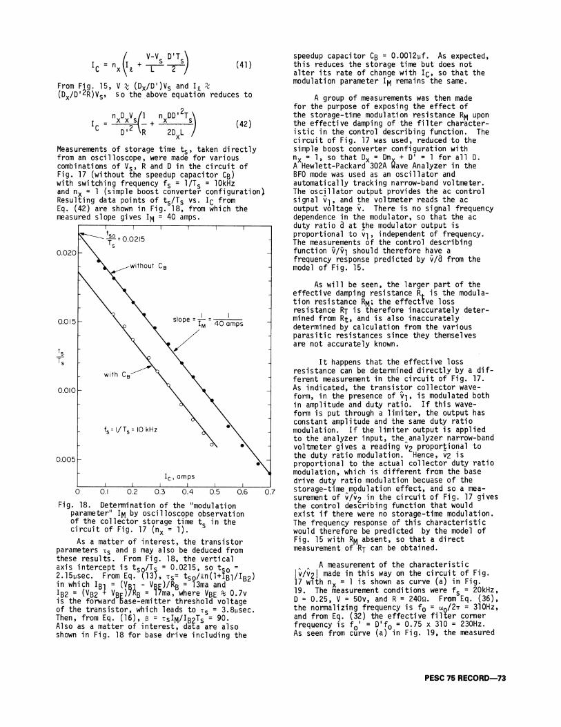
Measurements of storage time t s , taken direct ly from an osc i l loscope , were made for various combinations of V s , R and D in the c i rcu i t of F ig . 17 (without the speedup capacitor Cß) with switching frequency f s = 1/TS = 10kHz and n x = 1 (simple boost converter configuration) Resulting data points of t s / T s vs . I Q from Eq. (42) are shown in F ig . 18, from which the measured slope gives Iyi = 40 amps.
0 . 0 2 0
0 . 0 1 5
0 . 0 1 0
0 . 0 0 5
- ^ = 0 . 0 2 1 5 1 s
- w i t h o u t C B
I M 4 0 a m p s
Fig. 18. Determination of the "modulation parameter" 1^ by osci l loscope observation of the col lector storage time t s in the c i rcu i t of Fig. 17 ( n x = 1).
As a matter of interest , the t ransis tor parameters T s and 3 may also be deduced from these r e s u l t s . From Fig . 18, the vert ical axis intercept i s t S 0 / T c = 0.0215, so t s o = 0 l r From Eq. (13), x s = t S 0 / i n ( ] + l ^ / l S 2 ) 2.15ysec. in which I B i = ( V B i - V D C ) / R B =T3ma and"
Iß2 = ( VB2 + V B F ) / ^ B = ' ' m a > where VßE % 0.7v is the forward base-emitter threshold voltage of the t rans is to r , which leads to T s = 3.8ysec. Then, from Eq. (16), 3 = T S I M / I B ? T S = 9 0 -Also as a matter of in terest , data are also shown in F ig . 18 for base drive including the
speedup capacitor Cß = 0.0012yf. As expected, th is reduces the storage time but does not al ter i t s rate of change with Ι ς , so that the modulation parameter I|vj remains the same.
A group of measurements was then made for the purpose of exposing the effect of the storage-time modulation resistance R^ upon the effective damping of the f i l t e r characteri s t i c in the control describing function. The c i rcu i t of F ig . 17 was used, reduced to the simple boost converter configuration with n x = 1 , so that D x = Dn„+ D' = 1 for a l l D. A Hewlett-Packard 302A Wave Analyzer in the BFO mode was used as an o s c i l l a t o r and automatically tracking narrow-band voltmeter. The o s c i l l a t o r output provides the ac control signal v-j, and the voltmeter reads the ac output voltage v. There i s no signal frequency dependence in the modulator, so that the ac duty rat io α at the modulator output i s proportional to v-j, independent of frequency. The measurements of the control describing function v/v-j should therefore have a frequency response predicted by v/d from the model of F i g . 15.
As wi l l be seen, the larger part of the effective damping resistance R. i s the modulat ion resistance R^; the effective loss resistance Rj i s therefore inaccurately determined from Rt , and i s also inaccurately determined by calculat ion from the various paras i t ic resistances since they themselves are not accurately known.
I t happens that the effective loss resistance can be determined di rect ly by a d i f ferent measurement in the c i r c u i t of F ig . 17. As indicated, the t ransis tor col lector waveform, in the presence of v-j, i s modulated both in amplitude and duty ra t io . I f th is waveform i s put through a l imi ter , the output has constant amplitude and the same duty rat io modulation. I f the l imi ter output i s applied to the analyzer input, the^nalyzer narrow-band voltmeter gives a reading V2 proportional to the duty rat io modulation. Hence, V2 i s proportional to the actual col lector duty rat io modulation, which i s different from the base drive duty rat io modulation becuase of the storage-t ime^odulat ion e f fect , and so a measurement of v / V 2 in the c i rcu i t of F ig . 17 gives the control describing function that would exist i f there were no storage-time modulation. The frequency response of th is character ist ic would therefore be predicted by the model of Fig. 15 with R|vj absent, so that a direct measurement of Rj can be obtained.
A measurement of the character ist ic |v /voJ made in th is way on the c i rcu i t of F ig . 17 with η χ = 1 i s shown as curve (a) in F ig . 19. The measurement conditions were f s = 20kHz, D = 0.25, V = 50v, and R = 2 4 0 Ω . From Eq. (36), the normalizing frequency i s f 0 = ωρ/2π = 310Hz, and from Eq. (32) the effective f i l t e r corner frequency i s f r = D ' f o - 0.75 χ 310 = 230Hz. As seen from curve (a) in F ig . 19, the measured
PESC 75 RECORD—73

ι 1 JF Q ' = I 3 d b
db
I ι ι ι ι I ι ι ι ι I 10Hz 2 0 4 0 6 0 8 0 1 0 0 I kHz
Fig . 19. Exposure of effect of modulation resistance RM on the control describing function peaking factor Q' in the c i rcu i t of F ig . 17 with n x = 1 and D = 0.25; (a) determination of R t = 1.2Ω from observed Q' = 13db; (b ) , ( c ) , (d) predicted lower Q' when various calculated values of RM are included, and observed data points .
corner frequency i s essent ia l ly equal to th is predicted value. Curve (a) also indicates that the peaking factor i s Q' = 13db -> 4.47. From Eq. (35), the total effective damping is due to Qt, Qi » and Q c ; for the present case, from Eqs. (38) and (39), Q c = u ) 0 L / R c = 11.4/0.28 = 41 in which R c = 0.28Ω i s the capacitance es r , and QL = R/cu 0L = 240/11.4 = 21. Then, with use of the measured Q' = 4.47, Eq. (35) may be solved to give Q t = 9.39. F ina l ly , from Eq. (37) with R t replaced by R t because Rjvj i s absent under the conditions of th is measurement, Rj = W g L / Q t = 1.2Ω. This i s a reasonable value, since for n x = 1 R u i s the total inductor resistance R = R a
+ R k = 0.46Ω, which leaves 1.2 - 0.46 % 0.7Ω for the remaining paras i t ic resistances.
With R T thus direct ly determined from the response v/v2> attention can be returned to the actual control describing function v/v-i in which the modulation resistance R^ i s present in the model of F ig. 15. Curve (b) in F ig . 19 shows I v/v-j I for the c i rcu i t of F ig . 17 under the same conditions as for curve ( a ) , namely f s = 20kHz, D = 0.25, R = 240Ω. For n x = 1 , the expression given by Eq. (26) i s R^ = V/1|vj = t S V / 3 I B ? T S . A s previously determined by independent measurement, Ijvj = 40 amps for f s = 10kHz; therefore, since 1^ is proportional
to the switching period T s , I M = 20 amps under the condition f s = 20kHz for curve (b) in F i g . 19, and then R M = V / I M = 50/20 = 2.5Ω. With use of the value Rj = 1.2ω already found, the total effective series damping resistance in the model of F ig . 15 is R t = R j + R T = 2.5 + 1.2 = 3.7Ω, which from Eq. (3/) gives Q t = i o 0 L / R t = 11.4/3.7 = 3.08. Then, from Eq. (35) with QL = 21 , Q c = 41, and D = 0.25, the total effective peaking factor i s Q' = 1.94 -> 6 db. The direct measurement of curve (b) shows a Q' of about 5db, so that the presence of the modulation resistance R|vj = 2.5Ω in the model of F ig . 15 accounts both qual i ta t ive ly and quantitat ively for the considerable lowering of the peaking factor by about 8db.
Another result due to R^ i s a change in effective f i l t e r peaking factor Q1 with change of voltage operating level or of switching frequency, which would not occur in the absence of the storage-time modulation effect . In the simple boost converter with η χ = 1 , Rjvj = V/ÏM = T s V / ^ B 2 T s and is therefore proportional to both V and t s = 1/T S . Curve (c) in F ig . 19 shows the control transmission character ist ic under the same conditions as for curve (b) except that V s i s halved, which s imi lar ly scales a l l the dc values, including the output voltage V. Hence, for I M = 20 amps, Rjvj i s halved to 1.25Ω and Rj stays the same at 1.2Ω, so that Rt = 2.45Ω. With a l l other quantit ies the same, Q' = 2.90 + 9db which agrees well with the measured value of 8db in curve (c ) . Al ternat ive ly , i f V i s restored to 50v but the switching frequency i s halved to f s = 10kHz, I M doubles to 40 amps and Rjvj = 1.25Ω again, so that Q1 remains at 9db, which is the value measured in curve (d) in F ig . 19.
Attention i s now turned to measurements under conditions that expose the r ight hal f -plane zero O K in the model of Fig. 15. S t i l l for the simple boost converter configuration η χ = 1 , measurements of the control describing function ν/ν·| were taken on the c i rcui t of F i g . 17 under the condition f s = 20kHz, D = 0.6, V = 25v, and R = 162Ω. ^ a t a points of both magnitude and phase of v/v-j are shown in F ig . 20. The phase measurements were also taken with the Hewlett-Packard 302A Wave Analyzer, by techniques that have been described e lse where [3]. The control describing function predicted by the model of F ig . 15 is obtained as fol lows.
The normalizing frequency i s f ç = 310Hz, and from Eq. (32) the effective f i l t e r corner frequency i s f 0 ' = D ' f 0 = 0.4 χ 310 = 130Hz. From Eqs. (38) and (39), Q c = 41 and Q, = 14. At f = 20kHz, Ijyj = 20 amps and the corresponding Modulation resistance i s Ry| = V / I ^ = 25/20 =1,25ω. With the paras i t ic loss resistance s t i l l Rj = 1.2ω, the total effective series damping resistance is R t = R M + Rj = 2.45Ω, so from Eq. (37) Q t = 4 .61. men, from Eq. (35), the effective peaking factor i s Q' = 1.37 -> 3db. Next, from Eq.
74—PESC 75 RECORD

1 ι 1 I ' . • e Q ' = 3 d b
1 l l | ' ' I _
k o „ 0 ΝΛ'=Ι30Ηζ\ magnitude^
— predicted --
- -90° NR. \ #
• measured lOdb
--180° \ °
\ Ο V . ·
\· ° Q
-
- -270° phase'- y /
— predicted
~° u ο ο ο Ο " "0*73 ΰ" υ -
° measured fA = -720 Hz fs = 20 kHz N
simple boost : n x= 1 —· f z = 13 kHz
^ . 1 -
ι I ι , Ι 1 Ι Ι ι 1
ι ι i i |
" Ι ν 1. ( a )
t
• •
ι l l | ^ Q ' =9db
• •
τ " —ι 1 1 —
1^1 V = 25v (R M absent)
\ ·
fs = 20 kHz *»
( b ) . - · . 0'=2dbSj
• \ / V = 25v:
/ R M = 4 . o n
- I (c)
\ · \
\ · \
\ · X lOdb
\f V = 5 0 v : , Λ , r m = s . o n V v,
( R M present)
" •«&yQ /=-2db\»
î \ \ f0' = 2 3 0 H z \ * \
tapped boost: n x
. ι , , 1
= 2
ι i l l
\ · \ V fa =-5.8 kHz"
\ V 1
1 - l 1 U , I , L_J
100 Hz I kHz 10
Fig. 21. Exposure of effect of and the r ight half-plane zero ω on the control describing function in the c i rcu i t of F ig . 17 with n x = 2 and D = 0.25: (a) determination of Rj = 2.3Ω from observed Q' = 9db; (b ) , (c) predicted lower Q' when various calculated values of R|v| are included, and observed data points .
resistance i s then R t = RM + R T = 4.0 + 2.3 = 6.3Ω, which leads to Q t = 1.81 and a total effective peaking factor Q' = 1.22 ^ 2db, in good agreement with the observed value in curve (b) of F ig . 21. From Eq. (34), the r ight half-plane zero i s f a = - ( n x D ' 2 Q , / D x ) f = -(2 χ 0.752 χ 21/1.25)310 = -5.8kHz, a lso in good agreement with curve (b) of F ig. 21.
As a further check on the model, the previous set of measurements was repeated with al l dc levels doubled, so that V = 50v. The results are shown in curve (c) in F ig . 21; the only predicted change i s that Rjvj i s doubled because V is doubled, so Rjv| = 8.0Ω. Then, Rt = 8.0 + 2.3 = 10.3Ω so Qt = 1.1 which leads to Q' = 0.77 -> -2db, in good agreement with curve (c) of F ig . 21.
F ina l ly , some sets of measurements of the control describing function were made for the generalized tapped-inductor boost converter with an input f i l t e r . The experimental c i rcu i t with inductor tap at η χ = 2 i s shown in F ig . 22, and the t rans is tor drive conditions and the converter inductor and capacitor were the same as in F ig . 17. Independent measurements led to the input f i l t e r element values L s = 3.2mh, C s = 12yf, R 5 = 3.5Ω including the capacitor esr . The switching frequency was 20kHz.
Prediction of results from the c i rcu i t of F ig . 22 can be made from the general con-
100 Hz I kHz 10 kHz
Fig. 20. Exposure of effect of r ight hal f -plane zero ω ά on the control describing function in the c i rcu i t of F ig . 17 with n x = 1 and D = 0.6: the maximum phase lag exceeds 180°.
(33), f = Q c f 0 = 41 χ 310 = 13kHz, and from Eq. (347 (with n x = 1 and D x = 1) f a = - D , 2 Q , f 0 = - 0 . 4 2 χ 14 χ 310 = -720Hz. Thus, a l l the parameters in the control frequency response of Eq. (31) are known, and the corresponding predicted magnitude and phase asymptotes are shown in F ig . 20 for comparison with the measured data points. I t i s seen that agreement i s quite good; in par t icu lar , i t may be noted that the phase exceeds 180° lag as i s expected from the r ight half-plane zero f 4 ; the phase f a i l s to reach 270° lag because of the le f t half-plane zero ω ζ due to the capacitance esr .
Further series of measurements were made on the c i rcu i t of F ig . 17 in the tapped-inductor condition with n x = 2. A f i r s t set of data Λ
points for the control describing function v/v2 was taken under the conditions f s = 20kHz, D = 0.25, V = 25v, and R = 240Ω, and the results are shown in curve (a) in F ig . 2 1 . λ A S in the previous example with n x = 1 , the v/V2 character ist ic does not include the effect of R M , so that a direct measurement of the paras i t i c loss resistance may be obtained. From curve (a) in F ig. 21, the measured effective peaking factor is Q' = 9db -> 2.82, and Q c = 41 and QL = 21 as in the example with n x = 1 . Therefore, from Eq. (35), Q. = 4.9 and hence R x = 2.3Ω. Since the normalizing frequency i s f 0 = 310Hz, the effective f i l t e r corner frequency i s f 0 ' = D ' f 0 = 230Hz.
Λ Λ The actual control describing function v / V ] was then measured under the same condit ions, so that the effect of RM was included, and the results are shown in curve (b) in F ig . 21. The predicted value of R M i s obtained from Eq. (26), RM = n x 2 v / D x I M : for f s = 20kHz, I M = 20 amps as before; for n x = 2 and D = 0.25, D x = Dn x + D' = (0.25 ,x 2) + 0.75 = 1.25, so for V = 25v, R M = (22 X25)/(1.25x20) = 4.0Ω. The predicted value of the total effective series damping
PESC 75 RECORD—75

I_s= 3.2mh
Fig . 22. Experimental tapped-inductor boost converter with input f i l t e r .
tinuous model of F ig . 13. The dc and l ine transmission character ist ics are straightforward and wi l l not be discussed further. The nature of the control describing function i s not quite so obvious, and understanding of i t s sa l ien t qual i tat ive form i s fac i l i t a ted by some further steps in reduction of the model in order to f ind a simple equivalent driving generator proport ional to the ac duty rat io d.
Figures 23 and 24 show reduced forms of the general ac model of F ig . 13 that are analogous to those of F i g s . 14 and 15, but with retention of the input f i l t e r whose effect i s represented by i t s source impedance Z s looking back into
Rt
Fig. 23. Pa r t i a l l y reduced version of averaged model of F ig . 13 for determination of the control describing function ν / α , with input f i l t e r .
(±) v d l = e - ( R , + sL)7
- A V ^ ·· RT
D (V + v)
( î ) v d 2 = D / Z s ( - j, + j 2
Λ n x Γ s . / D x \ 2 Ζ 5Ί Rt
Vd
V ,2 >D R c
D R> D VC = D'V
-±r D XV 0 = D X D x = D n + D '
Fig. 24. Fully reduced version of model of F ig . 23, showing appearance of a minimum or possibly a null in the effective driving signal v d , in the neighborhood of the input f i l t e r resonant frequency ω δ where Z s
reaches a maximum.
the power supply as indicated in F ig . 22. As seen from Fig . 24, the total effective driving generator Vç| consists of the generator v ^ , previously ident i f ied in F ig . 15 as
v dl ( R A
+ s L ) J 2
j t i l •+ — Vd D x \ " a .
(43)
(44)
and an additional generator v ^ result ing from the presence of Z $ given by
\ i2 = D x 2 Z s ( f c 3] + h) (45)
From Eqs. (4) and (5 ) , this generator can be expressed as
2 η V Λ
ν .ο = D / Z c — — 5 - d d2 χ s D D , 2 R
(46)
in which the dc relation I n = V/D'R has been used. Hence, the total effective driving generator in F ig . 24 i s
\2 7 Ί
U ω ά \ d ' / R j Vd (47)
With substi tut ion for the frequency dependence of the source impedance Z s , Eq. (47) becomes
ν , η d _ χ Vd D
where
1 + — - ( ^ D'
2 κ ^ Ν β ) ] ' * i(k) * (k) s ' -J
(48)
(49)
The sa l ient features of the control describing function in the presence of the input f i l t e r can now be seen by inspection of the reduced model of F ig . 24, and Eq. (48). The source impedance Z s goes through a maximum value of about Q s ^ / R
s
a t approximately i t s resonant frequency ω 5 , so that Vd goes through a corresponding minimum value. In fac t , the minimum could actual ly be a null i f conditions are such that 2
This condition i s a function of dc duty rat io D. For the numerical values in the experimental c i rcu i t of F ig . 22, Qs = 4.66 and Eq. (51) predicts that a null should occur at D ^ 0.28. Computer solution of the model of F ig . 24 with Vd given by Eq. (48) showed that a null in the control describing function v/d actual ly occurred at D = 0.29. Further ins ight into the results was obtained by computer solution for the pole-zero locations of the control describing function for th is value of D and for another on either side of this value, namely D = 0.20, 0.29, and 0.5. Numerical values used were V s = 14v for D = 0.20, 0.29 and V s = 9.9v for D = 0.5; R M = V / I M with
76—PESC 75 RECORD

IM = 20 amps; and the value Rj = 2.3Ω previously determined for the n x = 2 converter was used for a l l three values of D, even though i t s value actual ly varies s l i g h t l y with D.
s - p l a n e
a ,b ,c
-13 kHz
-Ar-
8? -300-200-100 A
I
300
200
100 kHz
0
0 ΙΟΟΗζ I kHz 2 X f- 100 Hz
b a
-o-
X X
a: D = 0 . 2 0 , V s = Ι4ν
b: D = 0 . 2 8 , V s = I4v
c : D = 0 . 5 0 , V s =9 .9v
Fig . 25. Computer-calculated pole-zero pattern in the s-plane for the control describing function ν/α obtained from the model of F ig . 24 for the c i rcu i t of F ig . 22. A null occurs at D = 0.29 when the complex zero pair crosses the imaginary ax is .
f s = 2 0 k H z ^ .
D = 0 . 2 0 , V , = 14 ν
10 db
1 0 0 Hz I kHz 10 k H z
Fig . 26. Computer-calculated magnitude and phase of the control describing function for pole-zero pattern (a) in F ig . 25, showing the minimum in the magnitude response.
The results for the pole-zero posit ions are shown in F ig . 25. The l e f t half-plane zero, lower-frequency complex pole pai r , and the r ight half-plane zero represent the basic response of the converter effective low-pass f i l t e r , with the expected position-dependence upon D. The higher-frequency complex pole pair and complex zero pair represent the response due to the input f i l t e r , whose posit ions also depend upon D. In par t icu lar , i t i s noted that the complex
f s = 2 0 k H z N i
10 db
1 0 0 H z I kHz 10 kHz
Fig. 27. Computer-calculated magnitude and phase of the control describing function for pole-zero pattern (b) in F ig . 25, and data points obtained from the experimental c i r cuit of F ig. 22, showing the null in the magnitude response.
•0'
- 9 0 °
- 1 8 0 '
- 2 7 0 ° phase :
— pred ic ted
- 3 6 0 ° / ° m e a s u r e d
m a g n i t u d e : — p r e d i c t e d -
• m e a s u r e d - l O d b
f s = 2 0 k H z .
D = 0 . 5 0 , V s = 9 . 9 v
1 0 0 H z I kHz 10 k H z
Fig . 28. Computer-calculated magnitude and phase of the control describing function for pole-zero pattern (c) in F ig . 25, and data points obtained from the experimental c i rcu i t of F ig . 22, showing the large phase lag at high frequencies.
PESC 75 RECORD—77

zero pair crosses from the le f t half-plane to the r ight half-plane as D increases, with the expected null at D = 0.29.
The magnitude and phase plots corresponding to the three sets of computed pole-zero p o s i t ions are shown in F i g s . 26 through 28. Data points d i rect ly measured in the c i rcu i t of F ig . 22 are also shown for two of the sets of condit ions .
I t i s seen that good agreement i s obtained between the measured results and the prediction of the model of F ig. 24. From a practical point of view, the chief s igni f icance i s that a minimum in the control describing function can ex is t as a consequence of the presence of an input f i l t e r , and for a certain dc duty rat io the minimum could become a n u l l . I t i s noteworthy that a null can occur in spite of f in i te Qs (nonzero R ? ) in the input f i l t e r . Thus, i f such a converter were part of a regulator, normal internal adjustment of the dc duty ratio could cause a null in the loop ga in . Even more ser ious, values of dc duty rat io D greater than that for which the null occurs lead to a very large phase lag at high frequencies, much larger than for smaller values of D. This i s a consequence of the movement of the complex zero pair from the l e f t half-plane to the r ight hal f -p lane. Therefore, very severe regulator s t a b i l i t y problems could be experienced unless great care i s exercised in the design.
5. CONCLUSIONS
A s m a l l - s i g n a l , low-frequency, averaged model for the tapped-inductor boost converter with input f i l t e r has been developed and experimentally ver i f ied . The general model i s shown in Fig. 13, and from i t the dc transfer function and the ac l ine and control describing functions can be obtained.
The model of F ig . 13 i s obtained pr inc ipa l ly by manipulations of the c i rcu i t diagrams rather than by algebraic a n a l y s i s , so that physical ins ight into the s igni f icance of the steps i s retained throughout the derivat ion. In the absence of an input f i l t e r , the ac l ine and control describing functions are characterized by an effective low-pass f i l t e r described by a pair of le f t half-plane poles and a le f t half-plane zero; the control describing function has in addition a r ight half-plane zero. The posit ions of the poles and of the r ight half-plane zero change with dc duty rat io D.
The method of derivation of the averaged model i s a refinement of that described for the simple boost converter in [1] ; the refinement leads to a more accurate representation of the paras i t ic loss resistances in the model, and was an attempt to explain experimentally
measured values of the effective f i l t e r Q-factor that were substant ia l ly lower than those predicted by the or iginal model. However, i t was found that this refinement provided insuff ic ient quantitative correction, and that instead an entirely different effect was responsible for these lower Q-factors.
This new effect i s shown to be due to storage-time modulation in the t ransistor power switch, in which the effective duty rat io modulation at the col lector i s different from the driving duty rat io modulation at the base. The model of F ig . 13 incorporates th is effect in a modulation resistance R|v|, which i s shown enclosed in an oval as a reminder that i t i s to be included in the ac model only. The signi f icance of this result i s that the modulation resistance Rjv| contributes to the effective f i l t e r ac damping resistance but does not contribute to the effective dc loss r e s i s tance; consequently, the f i l t e r Q-factor is lowered, but the converter eff iciency is unaffected, by the presence of the modulation resistance R ^ . This resul t maybe considered a rare exception to Murphy's law, since the storage-time modulation effect produces a desirable damping effect without an associated undesirable loss of ef f ic iency.
Experimental measurements of both magnitude and phase of the control describing function are presented to verify the averaged model both qual i ta t ive ly and quanti tat ively. Experimental conditions were chosen spec i f i ca l l y to expose certain features of the model for individual ver i f ica t ion: for the simple boost converter of F ig . 17 with n x = 1 , F ig . 19 shows the damping effect due to the modulation resistance RJVJ and F ig . 20 exposes the r ight half-plane zero and associated excess phase l a g ; F ig . 21 shows the effect of Rjv| in the tapped-inductor converter with η χ = 2.
Experimental results are also presented for the control describing function of the system of F ig . 22, a tapped-inductor boost converter with η χ = 2 and with an input f i l t e r . The corresponding averaged model i s shown in F ig . 24, and the important feature i s that the control describing function acquires a complex pair of zeros that can move from the l e f t ha l f -plane to the r ight half-plane as the dc duty rat io D is increased, as would happen during normal adjustment in a practical closed-loop regulator. The signi f icance of this i s i l lus t ra ted in the magnitude and phase results of F i g s . 26 through 28, in which the magnitude plot has a minimum, in the neighborhood of the input f i l t e r resonant frequency, which actual ly becomes a null when the complex pair of zeros l i es on the imaginary a x i s . Furthermore, as the pair of zeros moves into the r ight hal f -plane, the magnitude null retreats to a minimum but the phase lag becomes exceedingly large. Unless recognized and properly accounted for , this effect could have disastrous effects upon the s t a b i l i t y of a closed-loop regulator.
78—PESC 75 RECORD

The physical ins ight into the nature of the properties of a tapped-inductor boost converter makes the averaged model a useful and easi ly applied design too l . The method of model derivation can be applied in a s imi lar manner to numerous other c i rcu i t configurat ions.
Thanks are due to Howard Ho and Alan Casse l , graduate students of the Cal i fornia Inst i tute of Technology, for their assistance in constructing the experimental converters and for the computer plots shown in F i g s . 26 through 28.
REFERENCES
[1] G. W. Wester and R. D. Middlebrook, "Low-Frequency Characterization of Switched dc-dc Converters," IEEE Power Processing and Electronics Spec ia l is ts Conference, 1972 Record pp. 9-20; a l s o , IEEE Trans. Aerospace and Electronic Systems, vol . AES-9 , no. 3, pp. 376-385, May 1973.
[2] C. L. Searle et a l , Elementary Circui t Properties of T rans is tors , SEEC vo l . 3, p. 284; John Wiley & Sons, 1964.
[3] R. D. Middlebrook, "Measurement of Loop Gain in Feedback Systems," International Journal of E lectronics , vo l . 38, no. 4, pp. 485-512, April 1975.
PESC 75 RECORD—79


![Modeling and Control of a Multi-stage Interleaved …by Cuk in buck-boost converter [6], [7]. In [8], Witulski has shown how a coupled inductor´ differs from normal inductor and transformer](https://img.dokumen.tips/doc/110x75/5f4d972268593756d475e471/modeling-and-control-of-a-multi-stage-interleaved-by-cuk-in-buck-boost-converter.jpg)