Embed Size (px)
Citation preview

A Configurable System-on-Chip Device Facilitates Customization
and Reuse
Danesh Tavana([email protected])
Steven K. Knapp([email protected])
S211

Agenda
• Embedded System Challenges• Industry Trends• The Next Logical Step: A Configurable
System-on-Chip• Technical Challenges
– System communication, device structure– Debugging – Maintaining hardware/software design flows
• Summary/Questions

The Embedded System Challenge
COMPROMISE!
Time toMarket
Perfor-mance
FeaturesPower
Cost Size

Industry Trends
• Advanced process technologies enable cost-effective system-on-a-chip designs and multi-million-gate FPGAs
• ASIC/FPGA densities now outstrip the capabilities to easily verify a design
• Adaptability is a desirable attribute• Integrating system logic (memory, CPU)
is expensive in FPGA logic

The Next Logical Step ...• Configurable System-on-Chip (CSoC)
– Pre-verified processor sub-system– Embedded programmable logic
Industry-Standard Processor
DedicatedUser Memory
ProgrammableLogic
Dedicated High Speed System Bus
CSoC
TelecomDatacom
Internet ApplianceNetworking
WirelessMobile Internet
High End ConsumerIndustrial Control
Many Others
Embedded SystemApplications

Configurable System-on-Chip • Pre-verified, configurable system
integrated on a single chip• Leverages standard logic design and
processor development tools• Leverages the design advantages of
both processors and programmable logic
• Fast time-to-market for embedded systems
• System-on-a-chip for the masses

Triscend E5 Configurable System-on-Chip
ConfigurableSystem Logic
(CSL)Matrix
PIOPIOPIOPIOPIO
PIO
8032"Turbo"Micro-
controller
PowerControl
Clock andCrystal
OscillatorControl
Power-OnReset
MemoryInterface
Unit
BusArbiter
Byte-wideSystem
RAM
JTAGInterface
HardwareBreakpoint
Unit
AddressMappers Add
ress
Bus
Dat
a B
us
Configurable SystemInterconnect (CSI) bus
Two-channel
DMAController
SelectorSelector
Selector
CSI Socket
8051/52Compatible
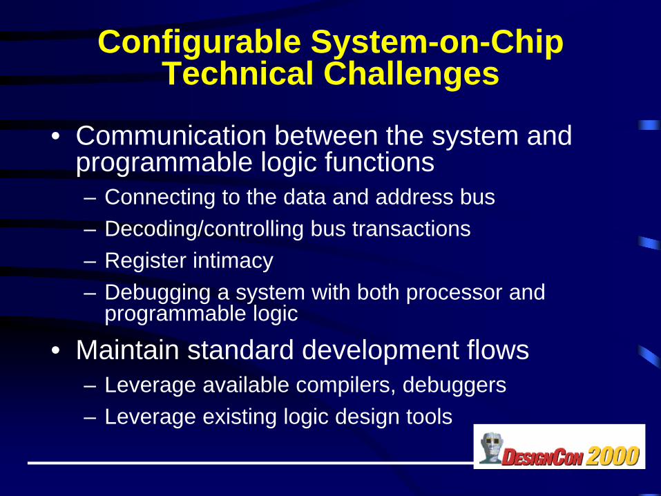
Configurable System-on-ChipTechnical Challenges
• Communication between the system and programmable logic functions– Connecting to the data and address bus– Decoding/controlling bus transactions – Register intimacy– Debugging a system with both processor and
programmable logic
• Maintain standard development flows– Leverage available compilers, debuggers– Leverage existing logic design tools

Two-Chip Solution: CPU+FPGA/ASIC
• I/Os between devices– Many pins required, even for
basic 8-bit interface– Adds delay to critical path– Extra power consumption and
EMI in two-chip solution
• Distributing address/data on-chip– Uses programmable interconnect– Adds delay to critical path– Variable delays in some
architectures– Some devices provide
bidirectional bussing
Proc
esso
r
DATA
ADDR
CONTROL
Write Decode Read Decode

?
Triscend Approach: CSI Bus Socket(Configurable System Interconnect)
Side-band Signals
CSI Socket Interface
Data Write
Data Read
Address
Sele
ctor
s
Bus Clock
Wait-StateControl
Con
figur
able
Sys
tem
Inte
rcon
nect
(CSI
) Bus
Con
figur
able
Sys
tem
Log
ic
(CSL
) Mat
rix
8032"Turbo"
Microcontroller
BreakpointControlHardware
Breakpoint Unit
DMA Request/Acknowledge
2-ChannelDMA Controller
• Distributes bus signals to embedded program-mable logic
• No I/O required• Predictable, synchronous
timing• Forward compatible with
future device families• Contention-free bussing • Wait-state control• DMA access• Integrated debugging

Selector
Match0
Match1
An A0A1A2
CSI Bus Address
RDSEL
WRSEL
READ
WRITE
BCLK
Bus Clock
RdSel
DATAData Read[7:0]
• Decode delay is constant(less than 5 ns after clock)
• Fast address decoding– Any address range– Access type
• Code• Data• Special Function
Register (SFR)Device SelectorsTE502 16TE505 32TE512 72TE520 128TE532 200

DMA Control Register(alternate Selector function)
REQSEL
ConfigurableSystem Logic
DM
A C
ontr
ol R
egis
ter
ACKSEL
DMAChannel 1
Request
Acknowledge
DMAChannel 0
Request
Acknowledge

CSL Cell Structure
Add
ress
Writ
e D
ata
RoutingMatrix
LUT FF
Data Read
LUT FF
CSL Cell = LUT+FF
• CSL cell perform various functions– Logic– Arithmetic– Memory– Bus– Sequential
• Intimate connection to the CSI system bus

CSL Logic StructureCSL Bank
• CSL = Configurable System Logic• CSI = Configurable System Interconnect
CSL Cell
CSI
Bus
Soc
ket
Selector
CSL Matrix
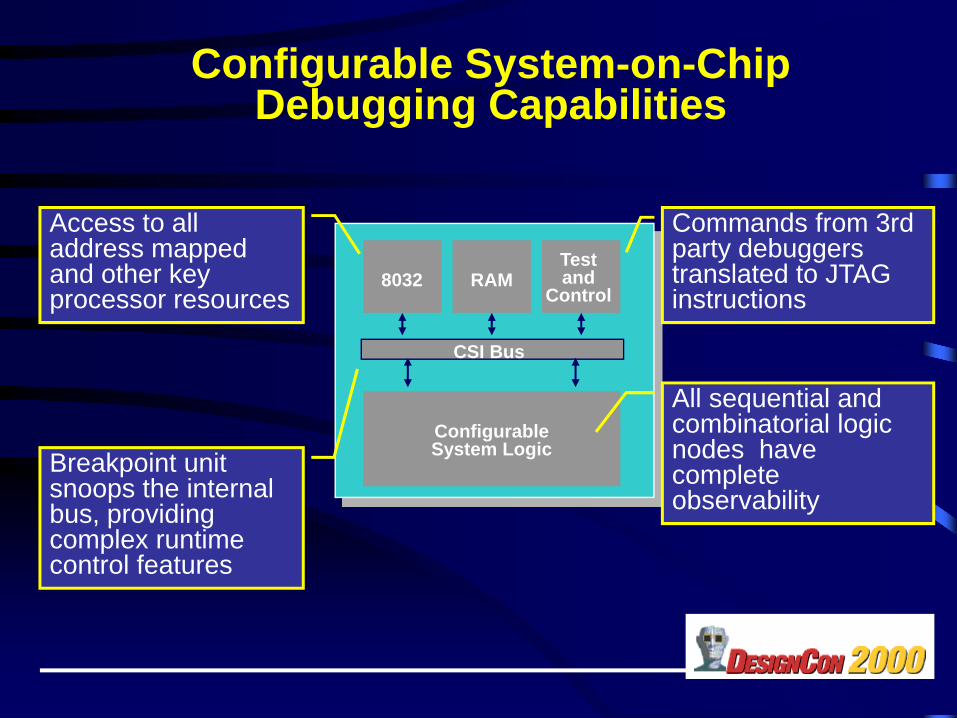
Configurable System-on-ChipDebugging Capabilities
8032 RAMTest and
Control
Configurable System Logic
CSI Bus
Commands from 3rd party debuggers translated to JTAG instructions
Access to all address mapped and other key processor resources
Breakpoint unit snoops the internal bus, providing complex runtime control features
All sequential and combinatorial logic nodes have complete observability

Triscend CSoC Design FlowTriscend FastChip™
Development Software
System Configuration
ProcessorDevelopment Tools
ProgramDevelopment
Designer’s standard tool flow
InstructionSimulation
NetlistCapture or Synthesis
FunctionalSimulation
3rd PartyEDA Tools
TriscendSoft Module
Library SourceCodeLibrary
DeviceProgramming
System Testand Debug
In-SystemDebug

FastChip Development System“Soft” Module
Library
DedicatedResources
“Soft” peripherals dragged intoCSL matrix
Resources UsedIndicators

Summary
• Advanced process technologies enable Configurable System-on-Chip devices
• High-density, cost-effective, and flexible
• Ideal for fast time-to-market for embedded systems applications
• On-chip communication, development flow, and debugging were top development challenges
• More to come ...

For More Information
www.triscend.com

Comparing 8052-class MCUsFeature
Average8052
Dallas80C320
PhilipsXA-GA
TriscendE5
8051/8052 binarycompatible Yes Yes No Yes
Max. Frequency 24 MHz 33 MHz 30 MHz 40 MHzInstruction cycle (clocks) 12 4 3 416-bit Timer/Counters 3 3 3 3+Watchdog Timer N/A Yes Yes YesUARTs 1 2 2 1+Interrupts 7 13 38 12+Data Pointers 1 2 - 2Wait-state support N/A N/A Yes YesPIO pins 32 32 32 60 to 316On-chip internal RAM 256 256 512 256On-chip MOVX RAM N/A N/A N/A 8K to 64KGlue-less memory interface N/A N/A N/A YesDMA channels N/A N/A N/A 2Maximum address space 64K 64K 1M/16M 64K/16MOn-chip debug hardware N/A N/A Yes Yes

Programmable I/O (PIO)
QEN
D
Flip-Flop/Latch
Input
RegisteredInput
Clock
ClockEnable
InputHysteresis
PAD
BusMinder™
DEN
QOutputEnable
DriveStrength
DEN
QOutput
DelayZero Hold
Time
4 mA or 12 mA drive
Optional pullup resistor, pulldown resistor,
or bus follower
3.3 V outputs,5 V-tolerant
Flip-flops in I/O padsfor improved setup,
clock-to-outputperformance

Comparing Logic Capacity
0
500
1000
1500
2000
2500
3000
3500
XC4003
/S05AT40
K05TE50
2
XC4005
XL/S10TE50
5AT40
K10
FLEX10K10
A
XC4010
XL/S20AT40
K20
XC4013
XL/S30TE51
2
XC4020
XL/S40AT40
K30
FLEX10K30
AXC40
28XL
TE520
AT40K40
FLEX10K50
AXC40
44XL
TE532
LUT+
FF P
airs
E505E512
E520
E532
• Triscend CSL cell = 1 LUT4+FF pair• Xilinx CLB = 2 LUT4+FF pair
• Altera FLEX LE = 1 LUT4+FF pair• Atmel logic cell = 1 LUT4+FF pair
E502