Embed Size (px)
Citation preview

University of South Carolina University of South Carolina
Scholar Commons Scholar Commons
Theses and Dissertations
2016
A Comparison Of FPGA Implementation Of Latency-Based Solvers A Comparison Of FPGA Implementation Of Latency-Based Solvers
For Power Electronic System Real-Time Simulation For Power Electronic System Real-Time Simulation
Matthew Aaron Milton University of South Carolina
Follow this and additional works at: https://scholarcommons.sc.edu/etd
Part of the Electrical and Electronics Commons
Recommended Citation Recommended Citation Milton, M. A.(2016). A Comparison Of FPGA Implementation Of Latency-Based Solvers For Power Electronic System Real-Time Simulation. (Master's thesis). Retrieved from https://scholarcommons.sc.edu/etd/3903
This Open Access Thesis is brought to you by Scholar Commons. It has been accepted for inclusion in Theses and Dissertations by an authorized administrator of Scholar Commons. For more information, please contact [email protected].
A COMPARISON OF FPGA IMPLEMENTATION OF LATENCY-BASED SOLVERS FORPOWER ELECTRONIC SYSTEM REAL-TIME SIMULATION
by
Matthew Aaron Milton
Bachelor of ScienceUniversity of South Carolina, 2015
Submitted in Partial Fulfillment of the Requirements
For the Degree of Master of Science in
Electrical Engineering
College of Engineering and Computing
University of South Carolina
2016
Accepted by:
Andrea Benigni, Director of Thesis
Jason Bakos, Reader
Cheryl L. Addy, Vice Provost and Dean of The Graduate School

c© Copyright by Matthew Aaron Milton, 2016All Rights Reserved.
ii

ABSTRACT
In the design of power systems, real-time simulation is a powerful tool to eval-
uate and validate designs before dedicating resources to develop such systems.
Through use of real-time simulation, one can study the behavior of a power sys-
tem in interaction with real, physical elements, all while avoiding the cost and risk
in constructing and testing such systems before a design is finalized. In recent
decades, effort has been made in the industry and academia to apply real-time
simulation to that of switching power converters through use of high-speed digital
signal processors (DSPs) and field programmable gate array (FPGA) devices. With
these existing approaches, individual converters have been successfully simulated
with relatively high switching frequency. At the advent of smart power grids of
ever growing size, with switching converters operating at over 100kHz switching
frequency, demand has increased to move high-fidelity, real-time simulation from
converter-level modeling to system-level to simulate these power systems com-
pletely. However, many of the current simulation methods have difficulty to scale
to system-level model size while maintaining capability to run in real-time for sys-
tems deploying high frequency converters. As such, efforts have been made to
explore new simulation approaches that can meet these requirements.
Simulation methods oriented towards high parallelism in their computations
are perfect candidates for scalable, system-level real-time simulation. Two such
methods include Latency-Based Linear Multi-step Compound Method (LB-LMC)
and Latency Insertion Method (LIM). These methods exploit sources of latency in
modeled systems to divide up computations into operations that can be performed
iii

simultaneously. Originally developed for software-based execution on traditional
processors and DSPs, these methods are implementable on FPGA devices to take
advantage of these devices hardware-based, low-latency execution and native par-
allelism.
In this work, FPGA implementations of the LIM and LB-LMC methods for
system-level real-time simulation of power systems are developed and compared
for scalability and implementation challenges. FPGA-based simulation engines are
developed for both methods on a Xilinx Virtex-7 FPGA evaluation platform. The
LB-LMC simulation engine was realized to operate in single or multiple pass ex-
ecution per simulation time step and apply mixed integration methods for model
computations of various electrical components and converters. This engine ap-
plies use of subsystem decomposition allowable by LB-LMC to reduce compu-
tation time costs and FPGA resources needed for larger power system models.
The LIM simulation engine was implemented to operate in a two pass, leapfrog
approach to compute simulation solutions every time step. A novel method to
handle converter switching action in LIM was developed to enable LIM to model
power switching converters. For both simulation engines, various power systems
were simulated in real-time with 50ns and below time steps, from a single three-
phase converter to an eight converter dual-bus shipboard power system. Simula-
tion accuracy of both methods’ FPGA implementation are compared to high pre-
cision software-based simulators. The scalability of each method in real-time was
analyzed and evaluated in terms of achievable time step, determined by compu-
tational delay, and resource usage on an FPGA. Finally, the FPGA implementation
of each method is compared for implementation challenges in modeling power
systems with these implementations.
iv

TABLE OF CONTENTS
ABSTRACT . . . . . . . . . . . . . . . . . . . . . . . . . . . . . . . . . . . . iii
LIST OF TABLES . . . . . . . . . . . . . . . . . . . . . . . . . . . . . . . . . viii
LIST OF FIGURES . . . . . . . . . . . . . . . . . . . . . . . . . . . . . . . . ix
CHAPTER 1 INTRODUCTION . . . . . . . . . . . . . . . . . . . . . . . . . 1
CHAPTER 2 BACKGROUND . . . . . . . . . . . . . . . . . . . . . . . . . . 4
2.1 Latency-Based Linear Multi-step Compound Method . . . . . . . . . 4
2.2 Latency Insertion Method . . . . . . . . . . . . . . . . . . . . . . . . . 7
2.3 FPGAs and Simulation Computation Implementation . . . . . . . . . 9
CHAPTER 3 LB-LMC REALIZATION ON FPGA . . . . . . . . . . . . . . . 13
3.1 FPGA Encapsulation . . . . . . . . . . . . . . . . . . . . . . . . . . . . 13
3.2 System Solver Realization . . . . . . . . . . . . . . . . . . . . . . . . . 15
3.3 Simulation Engine Composition . . . . . . . . . . . . . . . . . . . . . . 18
3.4 FPGA Implementation . . . . . . . . . . . . . . . . . . . . . . . . . . . 21
3.5 Test Models . . . . . . . . . . . . . . . . . . . . . . . . . . . . . . . . . 22
3.6 Implementation Results . . . . . . . . . . . . . . . . . . . . . . . . . . 24
v

CHAPTER 4 LIM REALIZATION ON FPGA . . . . . . . . . . . . . . . . . 30
4.1 FPGA Encapsulation . . . . . . . . . . . . . . . . . . . . . . . . . . . . 30
4.2 Simulation Engine Composition . . . . . . . . . . . . . . . . . . . . . . 31
4.3 Switching Power Converters in LIM . . . . . . . . . . . . . . . . . . . 32
4.4 FPGA Implementation . . . . . . . . . . . . . . . . . . . . . . . . . . . 38
4.5 Implementation Results . . . . . . . . . . . . . . . . . . . . . . . . . . 38
CHAPTER 5 SCALABILITY ANALYSIS . . . . . . . . . . . . . . . . . . . . . 42
5.1 LB-LMC . . . . . . . . . . . . . . . . . . . . . . . . . . . . . . . . . . . 43
5.2 LIM . . . . . . . . . . . . . . . . . . . . . . . . . . . . . . . . . . . . . . 45
5.3 Evaluation . . . . . . . . . . . . . . . . . . . . . . . . . . . . . . . . . . 47
CHAPTER 6 MODELING AND IMPLEMENTATION DISCUSSION . . . . . . . 52
6.1 LB-LMC Modeling on FPGA . . . . . . . . . . . . . . . . . . . . . . . . 52
6.2 LIM Modeling on FPGA . . . . . . . . . . . . . . . . . . . . . . . . . . 54
CHAPTER 7 FUTURE WORK . . . . . . . . . . . . . . . . . . . . . . . . . . 56
CHAPTER 8 CONCLUSION . . . . . . . . . . . . . . . . . . . . . . . . . . 59
REFERENCES . . . . . . . . . . . . . . . . . . . . . . . . . . . . . . . . . . 61
APPENDIX A LB-LMC ENGINE HLS C++ CODE . . . . . . . . . . . . . . 63
A.1 Capacitor Entity . . . . . . . . . . . . . . . . . . . . . . . . . . . . . . . 63
A.2 Inductor Entity . . . . . . . . . . . . . . . . . . . . . . . . . . . . . . . 64
A.3 Three Phase Half-Bridge Converter Entity . . . . . . . . . . . . . . . . 64
vi

A.4 Simulation Engine for Microgrid (Single Bus System) . . . . . . . . . 66
A.5 System Solver for Microgrid (Single Bus System) . . . . . . . . . . . . 68
APPENDIX B LIM ENGINE HLS C++ CODE . . . . . . . . . . . . . . . . . 73
B.1 Branch Entity . . . . . . . . . . . . . . . . . . . . . . . . . . . . . . . . 73
B.2 Node Entity . . . . . . . . . . . . . . . . . . . . . . . . . . . . . . . . . 73
B.3 Simulation Engine for Microgrid (Single Bus System) . . . . . . . . . 74
vii

LIST OF TABLES
Table 3.1 DC/AC Converter Model Parameters . . . . . . . . . . . . . . . . . 22
Table 3.2 Model Error for LB-LMC . . . . . . . . . . . . . . . . . . . . . . . . 26
Table 3.3 Resource Usage for Multi-cycle System Solver . . . . . . . . . . . . 29
Table 4.1 Model Error for LIM . . . . . . . . . . . . . . . . . . . . . . . . . . . 39
Table 5.1 LIM Scalability Results . . . . . . . . . . . . . . . . . . . . . . . . . 49
Table 5.2 LB-LMC Scalability Results . . . . . . . . . . . . . . . . . . . . . . . 50
viii

LIST OF FIGURES
Figure 2.1 Linear Networks with Nonlinear Components . . . . . . . . . . . 4
Figure 2.2 LB-LMC Solution Flow . . . . . . . . . . . . . . . . . . . . . . . . . 6
Figure 2.3 LIM Models . . . . . . . . . . . . . . . . . . . . . . . . . . . . . . . 7
Figure 2.4 LIM Time Base . . . . . . . . . . . . . . . . . . . . . . . . . . . . . . 8
Figure 2.5 Diagram of Example FPGA . . . . . . . . . . . . . . . . . . . . . . 9
Figure 2.6 Hardware Implementation of Difference Equation for LIMBranch Current . . . . . . . . . . . . . . . . . . . . . . . . . . . . . 11
Figure 3.1 Example of DC/AC Converter Component Entity . . . . . . . . . 14
Figure 3.2 Separation of Subsystems . . . . . . . . . . . . . . . . . . . . . . . 16
Figure 3.3 LB-LMC Simulation Engine . . . . . . . . . . . . . . . . . . . . . . 19
Figure 3.4 Finite State Machine for Multi-Cycle Simulation Engine . . . . . . 20
Figure 3.5 Three Phase DC/AC Converter . . . . . . . . . . . . . . . . . . . . 23
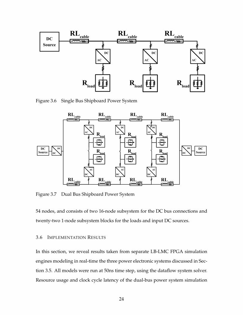
Figure 3.6 Single Bus Shipboard Power System . . . . . . . . . . . . . . . . . 24
Figure 3.7 Dual Bus Shipboard Power System . . . . . . . . . . . . . . . . . . 24
Figure 3.8 Top Level Design for Simulation Platform . . . . . . . . . . . . . . 25
Figure 3.9 Single-Bus Power System Analog Output under LB-LMC . . . . . 27
Figure 3.10 Dual-Bus Power System Analog Output under LB-LMC . . . . . 28
Figure 4.1 FPGA RTL Entities for LIM Models . . . . . . . . . . . . . . . . . . 31
ix
Figure 4.2 LIM Simulation Engine FPGA Design . . . . . . . . . . . . . . . . 32
Figure 4.3 Buck Converter . . . . . . . . . . . . . . . . . . . . . . . . . . . . . 33
Figure 4.4 Buck Converter LIM Model . . . . . . . . . . . . . . . . . . . . . . 33
Figure 4.5 Buck Converter Switching Action with LIM Model . . . . . . . . 34
Figure 4.6 Three-Phase AC/DC Converter as Inverter . . . . . . . . . . . . . 35
Figure 4.7 Three-Phase Inverter LIM Model . . . . . . . . . . . . . . . . . . . 35
Figure 4.8 Handling Switching Action in LIM Simulation Engine . . . . . . . 37
Figure 4.9 Analog Output for Single-Bus Power System under LIM Engine . 40
Figure 4.10 Analog Output for Dual-Bus Power System under LIM Engine . . 40
Figure 4.11 Deadband Interval Distortion Result . . . . . . . . . . . . . . . . . 41
Figure 5.1 Scalability Test Model . . . . . . . . . . . . . . . . . . . . . . . . . 48
Figure 5.2 Plot of LIM Scalability Results . . . . . . . . . . . . . . . . . . . . . 49
Figure 5.3 Plot of LB-LMC Scalability Results . . . . . . . . . . . . . . . . . . 51
x

CHAPTER 1
INTRODUCTION
In the design of power electronic systems, real-time simulation with hardware-in-
the-loop (HIL) techniques has in recent decades become an essential tool to eval-
uation and prototyping of new systems. The development and testing of power
electronic systems can be quite risky in terms of cost and safety, especially for high
power systems. Real-time simulation with HIL allows developers to reduce these
risks by emulating a portion of a system in actual time with a computational de-
vice or simulator, and then integrate this emulation with physical elements of the
system. Instead of having to construct a prototype of an unproven system por-
tion, one can use the simulation to observe the interaction of a system design with
physical components without dealing with the risks and costs of said prototype.
Examples of using HIL and real-time simulation for power electronic system ap-
plications are found in [1][2][3].
With the use of SiC-based, high-frequency switching converters in modern
power electronic systems, operating with switching frequencies of 100-200kHz
and greater, the need for small real-time simulation time steps to capture their
nonlinear dynamics has become a concern. These small time steps put tight time
constraints of the computational device used for the simulation. As such, a change
has occurred to move simulation from traditional computer processors to Digi-
tal Signal Processors (DSPs) and Field Programmable Gate Arrays (FPGAs) which
can compute for smaller time steps in real-time. In recent literature, various power
elements have been simulated entirely on FPGA, including a general power con-
1

verter, induction machine, and transformer [4][5][6], while a MMC converter has
been simulated with a CPU-and-FPGA mixed platform [7].
As the expansion of smart grids has grown in recent times, interest has in-
creased for real-time simulation for whole power electronic systems and grid-
connected power converters. Examples of current simulation work in this regard
are found in [8][9][10]. Many of these present approaches are not tailored for
scalable grid or system-level simulation of large power systems with numerous
converters and elements; especially for small time steps in real-time. Due to this
situation, effort has been made to develop methods for system-level real-time sim-
ulation.
For system-level, real-time simulation of modern power electronic systems,
scalable solver methods are needed to perform simulation of large models while
maintaining small time steps for high frequency dynamics. This scalability can
be achieved through the use of methods that exploit parallelism in their opera-
tions. One parallelizeable simulation method that exists is Latency-Based Linear
Multi-step Compound method (LB-LMC), defined in [11]. The LB-LMC method,
based on Resistive Companion method, exploits latency in components to sepa-
rate them from the system solution. This separation allows the components to be
solved in parallel before the system solver is complete. Besides the parallelism,
LB-LMC is suitable for real-time simulation due to predictable time steps, enabled
by pushing nonlinear elements into the components (which typically requires iter-
ative solving) and keeps the system solving side linear. Another method that fits
parallel execution well for real-time simulation is Latency Insertion Method (LIM),
first described in [12]. In LIM, circuits are modeled as branches and nodes with la-
tency inserted into each one. Applying this latency, the solutions for branches
and nodes can be separated and solved in parallel. All branches of a modeled
system are solved in parallel in one half time step and then the nodes are solved
2

all simultaneously in the remaining half time step. Solving the components with
non-iterative, explicit integration methods, the time step of LIM execution is fore-
seeable, making the method suitable for real-time execution like as with LB-LMC
method. To maximize parallelism and minimize computational delays for real-
time simulation, these methods can be readily implemented on FPGA devices to
exploit their native parallel execution and low hardware latencies, enabling time
steps below 50ns.
In this work, FPGA implementations of the LIM and LB-LMC methods for
system-level real-time simulation of power systems are developed and compared
for scalability and implementation challenges. Within Chapter 2, a brief overview
of these two simulation methods are discussed, followed by a discussion of FPGAs
and implementation of computations for these devices. Then, the FPGA realiza-
tion of LB-LMC method is presented in Chapter 3, detailing the encapsulation and
execution of this method on FPGAs, and providing demonstrating results for this
implementation. Afterward, in Chapter 4, the same coverage is given to the FPGA
implementation of LIM. With discussion of LB-LMC and LIM FPGA realization
covered, the scalability of the two methods in terms of computational delay and
resource usage are analyzed and tested, shown in Chapter 5. Finally, a short dis-
cussion on challenges and limitations of modeling power electronic systems with
these FPGA-implemented simulation methods is given in Chapter 6.
3

CHAPTER 2
BACKGROUND
2.1 LATENCY-BASED LINEAR MULTI-STEP COMPOUND METHOD
The Latency Based Linear Multi-step Compound Method (LB-LMC) is a highly
parallelizable simulation method designed for real-time simulation of dynamic
electrical systems. In this section we provide a summary description of this method
which is detailed in [11].
The LB-LMC method is derived from the Resistive Companion (RC) method,
solving dynamic systems as a set of linear equations Gx = b every simulation
time step, where G is the conductances of the system, b is the current contributions
of components, and x is the node voltages of the system. Unlike traditional RC
method, the LB-LMC method models all nonlinear components in a linear network
system as seen in Figure 2.1(a) as functional voltage sources with series resistance
(a) With Two Nonlinear Com-ponents
(b) With one Current-TypeNonlinear Component
Figure 2.1 Linear Networks with NonlinearComponents
4

or as shown in Figure 2.1(b), current sources with parallel conductance. These se-
ries resistances or parallel conductances are held fixed and are inserted into the G
conductance matrix to stay with standard form of RC components. The nonlinear
behavior of the nonlinear components are then reflected in the voltage or current
source that is updated every simulation step through an internal step that com-
putes the state equation of the component to update said source. The nonlinear
component state equations are expressed as:
dini
dt= f (v, i, xn
i , uni , t) (2.1)
dvnj
dt= f (v, i, xn
j , unj , t) (2.2)
, where v is the vector of the network node voltages, i is the vector of the network
branch currents, xni is the vector of the state variable internal to the i-th nonlinear
component, and ui is the vector of the input internal to the i-th nonlinear com-
ponent. Components with multiple terminals can be described by a mix of these
current and voltage sources. These equations are explicitly discretized to obtain:
Ini (k + 1) = f (v(k), i(k), xn
i (k), uni (k), k) (2.3)
Vnj (k + 1) = f (v(k), i(k), xn
j (k), unj (k), k) (2.4)
Since the state equations for Ini and Vn
j are explicitly discretized and only depend
on the solutions from previous time step, and the equations are independent from
one another, each nonlinear component can perform its internal step in parallel to
other components. From these state equations, the source contribution vector b
can be updated and the system solution each time step can be found with:
Gx(k + 1) = b(v(k), i(k), In(k), Vn(k), k) (2.5)
From having the conductance matrix G held constant due to consisting of only
fixed conductances, LU factorization for the LB-LMC method system solver can
5

Start
Build G,x,b from initialconditions
LU Factorization
t = t0
t = t + Δt
Forward and BackwardSubstitution
Ly = PbUx = y
Update vector b
T < TFinal
End Simulation
Yes
No
Initialize non linearcomponents(parallel)
Non linear componentsinternal step
(parallel)
Update across and through
values for xn
1
Update across and through
values for xn
i
(parallel)
Figure 2.2 LB-LMC Solution Flow
be performed offline, and only forward and backward substitution to solve the
system is performed each time step.
Figure 2.2 shows the solution flow for LB-LMC. In this flow, G, x, and b are
built from initial conditions and the LU factorization of the conductance matrix
is performed. Once all non-linear components are initialized, the simulation loop
begins. Each iteration consists of each component performing its own internal
step in parallel, then the source vector b is updated. From the updated b vector,
the system solution x is computed via forward and backward substitution and
saved for the next step. The simulation loop continues until final simulation time
is reached.
6

(a) Branch Model (b) Node Model
Figure 2.3 LIM Models
2.2 LATENCY INSERTION METHOD
LIM is a finite difference method for transient circuit simulation, first defined in
[12]. Beginning with a circuit having no latency, say a resistive network, reac-
tive latency is then inserted into all branches and nodes of a circuit so that branch
currents and node voltages both become continuous first-order functions of time.
Then it is possible to solve the networks through a set of algebraic steps as de-
scribed later. LIM has linear computational complexity and therefore it is highly
scalable; consequently, it strongly reduces the computational effort required for
the simulation of the network. A network has latency if each branch of the net-
work contains an inductance and each node of the network provides a capacitive
path to ground; if these values are not naturally present or if the present values
are small and thus present latency much smaller than the time features of interest,
additional capacitance or inductance can be added to increase latency (and hence
the allowable time step).
As shown in Figure 2.3(a) any generic branch is composed of a series combi-
nation of a resistance, an inductance and a voltage source; applying KVL to the
7

Figure 2.4 LIM Time Base
circuit of Figure 2.3(a), we can write the characteristic branch equation as:
Vn+1/2i −Vn+1/2
j = Lij
(In+1ij − In
ij
∆t
)+ Rij In
ij + En+1/2ij (2.6)
From equation (2.6) it is possible to calculate the unknown branch current:
In+1ij = In
ij +∆tLij
(Vn+1/2
i −Vn+1/2j − Rij In
ij + En+1/2ij
)(2.7)
Equation (2.7) must be computed for all the branches of the network at each time
step. As shown in Figure 2.3(b), each generic node is connected to ground via a
parallel combination of a conductance, a capacitance, and a current source; apply-
ing KCL to the circuit of Figure 2.3(b) we can write the characteristic node equation
as:
Ci
(Vn+1/2
i −Vn−1/2i
∆t
)+ GiVn+1/2
i − Hni =
Mi
∑j+1
Inik (2.8)
Where Mi is the number of branches connected to the node i. From equation (2.8)
it is possible to calculate the unknown node voltage:
Vn+1/2i =
CiVn−1/2i∆t + Hn
i −∑Mij=1 In
ikCi∆t + Gi
(2.9)
Equation (2.9) is computed for all the nodes of the network at each half time step.
Using a leapfrog approach, the current through each branch and the voltage at
each node can be updated alternately. The time is discretized and the current and
voltage quantities are allocated in half time step; see Figure 2.4. The leapfrog struc-
ture of LIM integration is very important for power electronics converter mod-
eling. It allows to represent ideal switching phenomena by linking nodes and
8

Figure 2.5 Diagram of Example FPGA
branches through their respective ideal voltage and current sources, with out in-
troducing any additional delay in the integration.
2.3 FPGAS AND SIMULATION COMPUTATION IMPLEMENTATION
In recent years, Field Programmable Gate Arrays (FPGAs) have been widely used
to perform real-time simulation of power systems. As seen in Figure 2.5, FPGAs
are programmable logic devices consisting of an array of Look Up Tables (LUTs),
Multiplexers (Mux), integer Digital Signal Processors (DSPs), and other digital
logic elements which can be programmatically configured and linked together to
create new digital circuits; examples of these circuits include signal switchers and
converters, computational units, and even complete processors. These circuits can
be created to operate independently from one another, enabling possibility of high
parallelism of operations on a FPGA. Moreover, due to the hardware nature of FP-
GAs, operations performed by logic circuits on them have low-latency compared
to performing same operations on a traditional processor or full DSPs. Integer op-
erations, for instance, can be performed on FPGAs in mere nanoseconds in com-
9

binational logic fashion while similar operations on a CPU can take microseconds,
requiring numerous clock cycles to compute result. From their high parallelism
and low-latency, FPGAs are ideal for handling computations needed for real-time
simulation.
Typically in software-based simulation, the use of floating-point data types,
such as IEEE 754, are used to represent numerical values in models due to their
high precision and dynamic range. However, computations with floating-point
data typically require complex, high-latency, pipelined operations to handle the so-
phisticated data format. Such operations can require large amount of resources on
a FPGA to implement, especially in using multiple computational units in parallel,
and induce computational delay which can impede the ability to reach nanosecond
time steps needed for real-time simulation of systems with high frequency dynam-
ics. An alternative to floating-point data types on FPGA is fixed-point representa-
tion. Fixed-point represents numerical values with fractional elements where the
decimal point is held fixed. Under fixed-point form, data bits before the decimal
point represent integral portion of a value, while bits after the point represent the
fractional part. Due to the simple and fixed nature of this data type, operations on
fixed-point values can be performed as if the values are whole integers. As such,
fixed-point operations can be easily instanced with simple combinational logic for
integer arithmetic which can execute in a pipeline-less, dataflow manner. Fixed-
point computational delay from this dataflow logic can depend almost solely on
propagation delay of the comprised logic primitives. Since fixed-point arithmetic
hardware is much simpler than floating-point hardware, the propagation delays
can be kept low. along with low resource usage and delay, many FPGA platforms
have built-in integer DSP slices or blocks which can be applied to accelerate opera-
tions and reduce delays of integer and fixed-point arithmetic. Despite the benefits
of using fixed-point, the main downside to using this numerical representation is
10
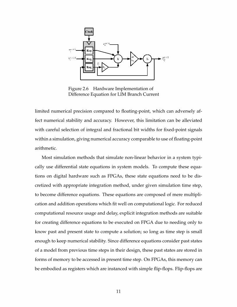
Figure 2.6 Hardware Implementation ofDifference Equation for LIM Branch Current
limited numerical precision compared to floating-point, which can adversely af-
fect numerical stability and accuracy. However, this limitation can be alleviated
with careful selection of integral and fractional bit widths for fixed-point signals
within a simulation, giving numerical accuracy comparable to use of floating-point
arithmetic.
Most simulation methods that simulate non-linear behavior in a system typi-
cally use differential state equations in system models. To compute these equa-
tions on digital hardware such as FPGAs, these state equations need to be dis-
cretized with appropriate integration method, under given simulation time step,
to become difference equations. These equations are composed of mere multipli-
cation and addition operations which fit well on computational logic. For reduced
computational resource usage and delay, explicit integration methods are suitable
for creating difference equations to be executed on FPGA due to needing only to
know past and present state to compute a solution; so long as time step is small
enough to keep numerical stability. Since difference equations consider past states
of a model from previous time steps in their design, these past states are stored in
forms of memory to be accessed in present time step. On FPGAs, this memory can
be embodied as registers which are instanced with simple flip-flops. Flip-flops are
11
state-based logic, so a digital clock is needed that drives the updates of the regis-
ters every time step. A complete FPGA implementation diagram of a difference
equation for LIM branch current (2.7) is seen in Figure 2.6.
12

CHAPTER 3
LB-LMC REALIZATION ON FPGA
3.1 FPGA ENCAPSULATION
In this section, the encapsulation of the LB-LMC method elements for FPGA im-
plementation is explained.
3.1.1 Component Entities
For each nonlinear component type used to model a system, a FPGA entity is de-
veloped. As input, these component entities take the system solution computed
in a previous time step. Along with system solution, component entities can also
take other input signals to control behavior of the entity, such as switch controller
signals for a DC/AC converter component. At the beginning of each time step, the
component entities sample and register their inputs. From these inputs and past
internal states, the components perform their internal step for (2.3) and/or (2.4)
and compute their source contributions.
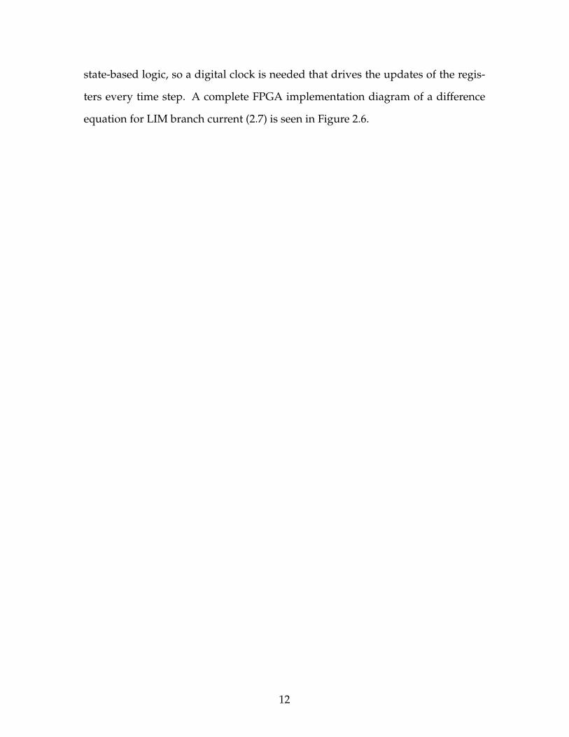
An example component entity for a DC/AC converter (see Figure 3.5) is de-
picted in Figure 3.1. The DC/AC converter entity takes five inputs that are the
DC bus and AC phase voltages on the terminals of the converter, and three switch
control inputs to control the output phase modulation. Each time step, the compo-
nent will register its past states and inputs from step k then use these to execute its
internal step. The internal step for the converter involves handling the switching
action of the converter through toggling bus capacitor voltages and filter inductor
13
DC/ACConverter
xDCi
xDCj
bACout1-3
SWCtrl1-3
XACout1-3
bDCi
bDCj
bDCi⇐vc1(k+1)GcapbDCj⇐vc2(k+1)Gcapb ACout 1⇐ il1(k+1)bACout 2⇐ il2(k+1)bACout 3⇐ il3(k+1)
vc 1(k+1)=Δ tC
(i p−ac 1−bc1−cc1)+vc 1(k )
vc 2(k+1)=Δ tC
(in−ac 2−bc 2−cc 2)+vc 2(k )
il1(k+1)=il1(k)+Δ tL
(a−X ACout 1(k )−Ril1(k ))
il2(k+1)=il2(k)+Δ tL
(b−X ACout 2(k)−Ril2(k ))
il3(k+1)=il3(k )+Δ tL
(c−X ACout 3(k )−Ril3(k ))
InputRegisters
i p=Gcap(XDCi−vc 1(k ))in=Gcap (XDCj−vc 2(k ))
a=v c1(k )(SWctrl1)+vc 2(k )(¬SWctrl 1)b=vc 1(k )(SW ctrl2)+vc 2(k )(¬SWctrl 2)c=vc 1(k )(SWctrl 3)+vc 2(k )(¬SW ctrl3)
ac 1=il1(k)(SWctrl 1)bc1=il2(k)(SWctrl 2)cc 1=il3(k )(SWctrl3)ac2=il1(k)(¬SWctrl 1)bc2=il2(k)(¬SWctrl 2)cc 2=il3(k )(¬SWctrl 3)
Figure 3.1 Example of DC/AC Converter Component Entity
currents (a, b, c, ac1, bc1, cc1, etc.) and computing the said capacitor and inductors
states for the current time step k + 1. The source contribution computational step
(dashed block) computes the source currents for the bus capacitors and feeds these
currents and the inductor currents out as the contribution output.
3.1.2 System Solver Entity
A dedicated system solver FPGA entity is created to compute the system solution.
This solver entity takes as input the component source contributions and accu-
mulates these contributions together to create the whole source vector b used to
compute the system solution. The entity provides the system solution vector x as
output which are fed back to component entities as input for the next time step
execution.
Unlike the original LB-LMC method, the system solver entity does not use
forward-backward substitution for system solution computation but instead uses
14

an inverted conductance matrix precomputed offline and multiple algebraic sum
of product (SOP) expressions to find system solution. In this approach, the sys-
tem solution is found by solving (2.5) for the vector x like in (3.1), where A is the
inverted G conductance matrix (A = G−1).
b = f (v(k), i(k), In(k), Vn(k), k)
x(k + 1) = Ab(3.1)
This solution is computed by expanding the multiplication between A and b
matrices into SOP expressions, like seen in (3.2), which are to be each computed
individually from one another. Since the inverted conductance matrix is fixed, the
A terms in the SOP expressions can be defined as constants in said expressions.
x = Ab⇒
A11b1 + A12b2 + · · ·+ A1nbn
A21b1 + A22b2 + · · ·+ A2nbn
...
An1b1 + An2b2 + · · ·+ Annbn
(3.2)
One main benefit of using this approach over forward-backward substitution is
division operations are not required in calculations which tend to be computation-
ally more expensive time-wise and use more FPGA resources compared to addi-
tion and multiplication operations. Moreover, this approach has only SOP expres-
sions for the system that can be solved for system solution elements in parallel. A
disadvantage to using this approach is that since the A matrix is precomputed of-
fline and the SOP expressions are dependent solely on the system being modeled,
the system solver entity and its expressions will have to be recreated or modified
for each new system that is to be simulated.
3.2 SYSTEM SOLVER REALIZATION
In this section, we detail how the system solver can be designed to realize desired
FPGA resource usage and computational latency.
15
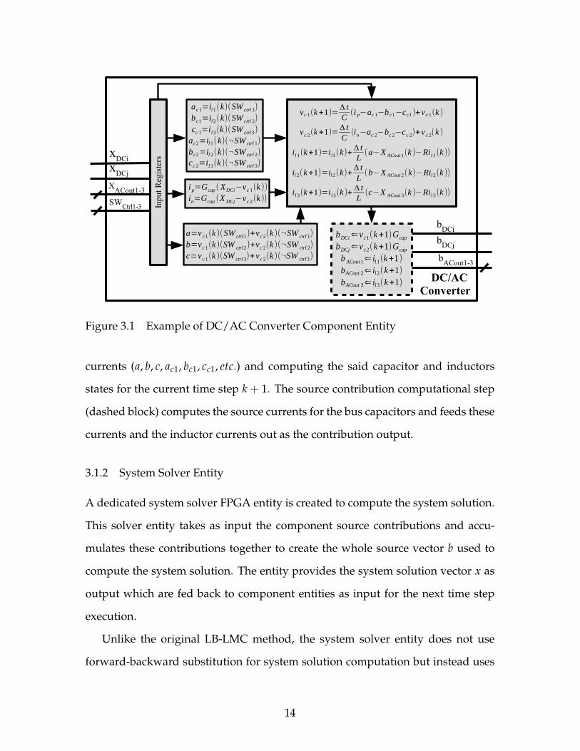
Figure 3.2 Separation of Subsystems
3.2.1 Subsystem Decomposition
Due to how the nonlinear behavior of components is moved to the source con-
tribution computations from the conductance matrix in LB-LMC, it is possible to
have multi-terminal components modeled as separate elements whose conduc-
tances are independent from one another. Then, the elements’ behavior is coupled
together via the component’s internal step to properly model the whole compo-
nent. From exploiting this separation of elements, the overall system model is
expressed to contain independent subsystems which appear as independent diag-
onal blocks on the conductance matrix. A subsystem solver can be created from
each diagonal block matrix and operated separately to compute a sub-vector of
the solution. These subsystem solvers can be encapsulated into the top level sys-
tem solver. The impact of using subsystem solvers is that the number of terms per
system solution equation can be reduced substantially, lowering amount of FPGA
hardware resources required.
16

An example of this subsystem separation for a 12-node system is shown in Fig-
ure 3.2. In this example, the system has two 4-node subsystem blocks and four
1-node blocks. If this system was solved without subsystem decomposition, 144
multiplications and 132 additions would be needed. However, with the decom-
position, the operations are reduced to 36 multiplication and 24 additions, signif-
icantly reducing resources needed for the system solver. The shipboard power
system models we present in this paper are expressed with a similar structure as
this example.
3.2.2 System Solver Architecture
The system solver is implementable using two types of architecture: dataflow that
solves solution equations in parallel within one pass, and multi-cycle which solves
solution equations in multiple iterations within single time step. These architec-
ture designs are explained below.
Dataflow Execution
In the dataflow implementation, the system solver solves all of its SOP solution
equations in parallel, computing solutions without delay as component source
contributions are produced. This approach allows solutions to be produced with
minimal delay induced from requiring multiple clock cycles. This method requires
that each solution equation has its own dedicated computational unit on the host
FPGA, composed of smaller combinational operator units for multiply and add
that are cascaded together in dataflow manner.
Multiple Cycle Execution
Another approach to implementing the system solver is to compute the system
solution in multiple clock cycles per time step. The computation operations of
17

the system solver are broken up into units which are reused and iterated every
clock cycle. Results from every iteration are compiled or accumulated to reach the
system solution. The reuse of the same computational units every iteration allows
reduction of FPGA resource usage for larger system models though at the expense
of additional computational latency per time step.
An effective usage of multi-cycle execution is to iterate the solving of each sub-
system block in a model. With such a setup, each subsystem block is solved each
cycle of the system solver. If a model has sizable but few subsystem blocks, then
using same subsystem solver and iterating it per subsystem can noticeably reduce
resource usage while maintaining low enough clock latency for nanosecond-range
time steps.
3.3 SIMULATION ENGINE COMPOSITION
This section provides explanation of how the entity encapsulations of the compo-
nents and system solver are linked together on FPGA hardware to perform simu-
lations.
To perform simulation of a system with the FPGA-adapted LB-LMC method,
a simulation engine like seen in Figure 3.3 is composed, consisting of multiple
component entities and one system solver entity tailored to the system simulated.
In the engine, a component entity for each nonlinear component of the system
is instanced and their source contribution outputs are linked to the appropriate
inputs of the instanced system solver entity. The system solution output of the
system solver is fed back to the component entities’ inputs, the components taking
solution elements that corresponds to their model terminals. If component entities
require input from peripherals such as a switch controller, the appropriate FPGA
elements are added to the design and linked to the requiring component entities.
The updates of the components is performed with a digital clock on rising edge.
18

Figure 3.3 LB-LMC Simulation Engine
The execution scheduling of the simulation engine depends on whether the
dataflow or multi-cycle system solver is used:
Single Pass with Dataflow System Solver
In use of the dataflow execution system solver, the simulation engine execution is
performed in one pass, bounded to a system clock whose period is equal to the
simulation time step. On the start of the time step, the component entities sam-
ple their inputs for the system solution from past time step and any peripheral
inputs. Then, the components perform their computations. As source contribu-
tions’ values are computed, the dataflow system solver will immediately compute
the current time step system solution without wait. The choice of time step clock
period is selected to be greater than the computational time needed by the simu-
19

Figure 3.4 Finite State Machine for Multi-Cycle Simulation Engine
lation engine. The time step is set to be greater than the computational delay so as
to ensure the simulation engine operates in stable manner.
Multiple Passes with Multi-cycle System Solver
For the simulation engine using the multi-cycle solver, the composition of the en-
gine is similar to the single pass design, but multiple clock cycles are required to
compute a system solution per time step period. In general, the component entities
will likely need fewer clock cycles or none to compute their solutions compared
to the multi-cycle system solver. Moreover, these component entities need to com-
pute their solutions before the solver can begin. As such, a finite state machine
is required to synchronize the execution of the component and system solver en-
tities to one another and to the simulation time step. This finite state machine is
20

created to have the component entities solve their contributions first, and then al-
low the system solver to compute the system solution. Once the system solution
is computed, the state machine has the engine wait until the beginning of the next
time step period. This state machine driven operation is shown in Figure 3.4. The
bounding of the entities’ solution computation to each engine state is done through
use of start input signals of each entity which is triggered by the state machine in
each state.
3.4 FPGA IMPLEMENTATION
We discuss in this section the implementation of the LB-LMC simulation engines
in regard to how computation execution is scheduled for parallelism and how nu-
merical quantities are stored and processed.
For high scalability of performance of the LB-LMC method on FPGAs, the par-
allelism of FPGA hardware is exploited to accelerate computations. To utilize this
high parallelism, all equation computations in component entities are expressed
to be executed independently where possible, allocated to dedicated arithmetic
units for each equation so that they can be solved in parallel. Furthermore, to
avoid serial data paths in component entity computations, solution equations are
expressed to avoid dependencies between one another where allowed by the com-
ponent’s model and solution integration method. Furthermore, all component en-
tities are instanced with independent hardware.
Parallelism is also exploited in the system solver. For the dataflow solver, all
system solution equations like seen in (3.2) are expressed to have dedicated arith-
metic hardware provided to each one so they can be scheduled to run simultane-
ously. Moreover, the equations are implemented in dataflow manner, as discussed
before, in the form of pure combinational logic composed of Lookup Table (LUT)
and DSP slices which compute new solutions as soon as source contribution results
21

Table 3.1 DC/AC Converter ModelParameters
VDC CDC_Bus LFilter CFilter RLoad12000 0.001 0.0001 1.0e-6 7.0
change. This execution manner allows solutions to be computed as soon as possi-
ble without having to wait for all source contributions to be computed by the com-
ponent entities. In the multi-cycle system solver, the solution equations, though
terms are looped, are also all implemented with separate hardware as well. Due to
the repeated use of the arithmetic hardware in the multi-cycle solver for each solu-
tion equation during each time step, this hardware is pipelined to reduce number
of cycles needed to reach a solution to be equal to number of terms per equation
plus any cycles needed to fill the pipelines.
So that computational delays for the component entities and system solver is
reduced and mostly dependent on the low propagation delays of the FPGA prim-
itives, fixed-point arithmetic logic is used instead of floating-point logic for all
calculations performed within.
3.5 TEST MODELS
In this section, the power electronic system models used to evaluate the LB-LMC
FPGA simulation engine is discussed. Each model is of increasing size and com-
plexity.
3.5.1 Three-Phase DC/AC Converter
A three-phase DC/AC converter, depicted in Figure 3.5, is modeled in LB-LMC
method using parameters seen in Table 3.5. The converter operates with 12kV DC
input. Switching frequency for the converter is 100kHz. The component entity of
the converter model separates its internal elements into independent subsystems
22
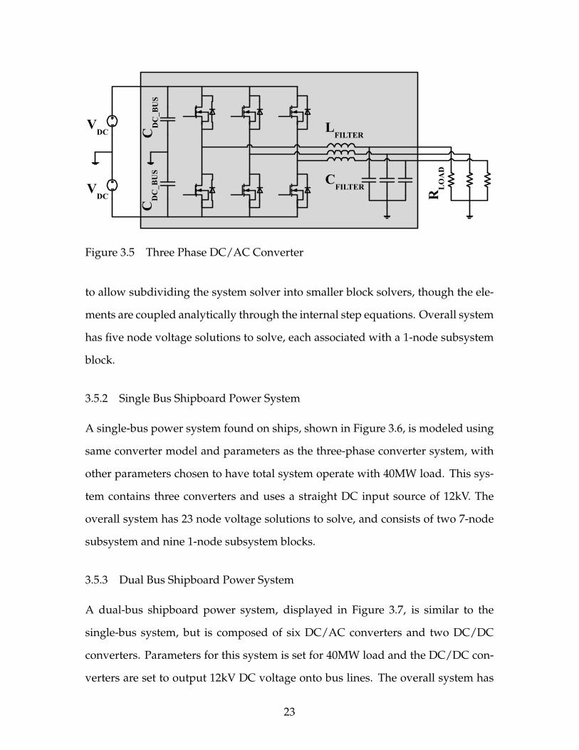
LFILTER
CFILTER
CDC_BUS
RLOAD
VDC
CDC_BUS
VDC
Figure 3.5 Three Phase DC/AC Converter
to allow subdividing the system solver into smaller block solvers, though the ele-
ments are coupled analytically through the internal step equations. Overall system
has five node voltage solutions to solve, each associated with a 1-node subsystem
block.
3.5.2 Single Bus Shipboard Power System
A single-bus power system found on ships, shown in Figure 3.6, is modeled using
same converter model and parameters as the three-phase converter system, with
other parameters chosen to have total system operate with 40MW load. This sys-
tem contains three converters and uses a straight DC input source of 12kV. The
overall system has 23 node voltage solutions to solve, and consists of two 7-node
subsystem and nine 1-node subsystem blocks.
3.5.3 Dual Bus Shipboard Power System
A dual-bus shipboard power system, displayed in Figure 3.7, is similar to the
single-bus system, but is composed of six DC/AC converters and two DC/DC
converters. Parameters for this system is set for 40MW load and the DC/DC con-
verters are set to output 12kV DC voltage onto bus lines. The overall system has
23
DCSource
DC
AC
DC
AC
DC
AC
RLOAD
RLOAD
RLOADRloadRload Rload
Rload
Rload
Rload
RLcable
RLcable
RLcable
Figure 3.6 Single Bus Shipboard Power System
DC
AC
DC
AC
DC
AC
AC
DC
AC
DC
AC
DC
DC
DC
DC
DC
DCSource
Rload
Rload
Rload
Rload
Rload
RLcable
Rload
Rload
RLcable
RLcable
RLcable
RLcable
RLcable
RLcable
RLcable
Rload
Rload
Rload
Rload
Rload
Rload
Rload
Rload
Rload
Rload
DCSource
Figure 3.7 Dual Bus Shipboard Power System
54 nodes, and consists of two 16-node subsystem for the DC bus connections and
twenty-two 1-node subsystem blocks for the loads and input DC sources.
3.6 IMPLEMENTATION RESULTS
In this section, we reveal results taken from separate LB-LMC FPGA simulation
engines modeling in real-time the three power electronic systems discussed in Sec-
tion 3.5. All models were run at 50ns time step, using the dataflow system solver.
Resource usage and clock cycle latency of the dual-bus power system simulation
24

Figure 3.8 Top Level Design for Simulation Platform
engine using the multi-cycle system solver is also presented to show the change in
results from moving to single-pass to multi-pass operation.
3.6.1 Setup
For all three models, the same top-level FPGA design was used, shown in Figure
3.8. The simulation engine was developed in C++ under Xilinx Vivado HLS 2015.4,
and the complete top-level design was composed in standard Vivado using VHDL
for the Xilinx Virtex-7 VC707 evaluation board; C++ code found in Appendix A.
All numerical operations in the simulation engine were performed with fixed point
logic defined with HLS ap_fixed library, using 72-bit width with 43-bit fractional
precision. The engine controller seen in Figure 3.8 handles the start and reset of
the simulation engine, as well as the wait state of the simulation engine’s finite
state machine when using a multi-cycle system solver. All models were run with
open-loop switching control to minimize impact of correcting control action on
simulation results.
25
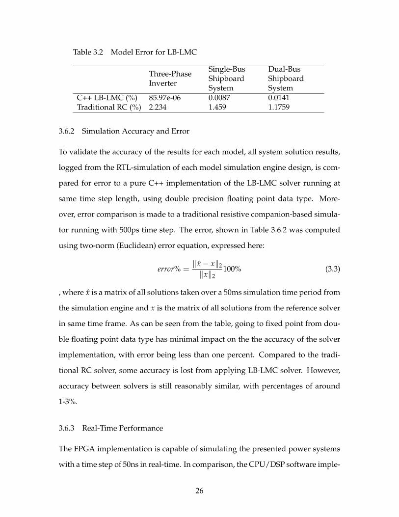
Table 3.2 Model Error for LB-LMC
Three-PhaseInverter
Single-BusShipboardSystem
Dual-BusShipboardSystem
C++ LB-LMC (%) 85.97e-06 0.0087 0.0141Traditional RC (%) 2.234 1.459 1.1759
3.6.2 Simulation Accuracy and Error
To validate the accuracy of the results for each model, all system solution results,
logged from the RTL-simulation of each model simulation engine design, is com-
pared for error to a pure C++ implementation of the LB-LMC solver running at
same time step length, using double precision floating point data type. More-
over, error comparison is made to a traditional resistive companion-based simula-
tor running with 500ps time step. The error, shown in Table 3.6.2 was computed
using two-norm (Euclidean) error equation, expressed here:
error% =‖x− x‖2
‖x‖2100% (3.3)
, where x is a matrix of all solutions taken over a 50ms simulation time period from
the simulation engine and x is the matrix of all solutions from the reference solver
in same time frame. As can be seen from the table, going to fixed point from dou-
ble floating point data type has minimal impact on the the accuracy of the solver
implementation, with error being less than one percent. Compared to the tradi-
tional RC solver, some accuracy is lost from applying LB-LMC solver. However,
accuracy between solvers is still reasonably similar, with percentages of around
1-3%.
3.6.3 Real-Time Performance
The FPGA implementation is capable of simulating the presented power systems
with a time step of 50ns in real-time. In comparison, the CPU/DSP software imple-
26

VO
LTA
GES
(V)
TIME (10ms/div)-0.02 0 0.02 0.04 0.06
-6000
-4000
-2000
0
2000
4000
6000
Figure 3.9 Single-Bus Power System Analog Output underLB-LMC
mentation of the LB-LMC method seen in [11] is only able to simulate in real-time
at 15µs for a micro-grid power system similar to the single-bus shipboard system.
The adaptation of the LB-LMC method from a software solution to a hardware
solution has allowed for substantial decrease in computational time while still en-
abling real-time simulation of larger models.
3.6.4 Demonstration
The simulation engine designs of the two shipboard systems are loaded onto the
VC707 FGPA board and analog output of each model was captured, via an oscil-
loscope, from their respective engine; results seen in Figures 3.9 and 3.10. For the
single-bus system model results, three AC output phases from one of the DC/AC
converters is shown. The dual-bus system results displays two of the output
phases and the positive and negative DC bus line voltages. The results for the
single-bus system were captured while switch control for the DC/AC converters
was set to reduce phase output voltage by half suddenly. Similarly, the dual-bus
system results were captured while the switch control of the DC/DC converters
27

VO
LTA
GES
(V)
TIME (10ms/div)-0.08 -0.06 -0.04 -0.02 0
-6000
-4000
-2000
0
2000
4000
6000
Figure 3.10 Dual-Bus Power System Analog Output underLB-LMC
powering the system was set to reduce bus voltage to simulate sudden drop in
DC/DC converter voltages. Ringing in the dual-bus system voltages is consistent
with traditional Resistive Companion Method version of said system, and is ex-
pected due to operating without closed-loop control to correct for the oscillations,
as well as the sudden change in voltage by the control.
3.6.5 Multi-cycle System Solver Resource Usage
To evaluate impact on resource usage from using a multi-cycle system solver with
subsystem iteration, the system solver for the dual-bus shipboard system was im-
plemented in Vivado with the dataflow design and the multi-cycle design for a
50ns clock cycle, where the dataflow is expected to compute its solution before
50ns while the multi-cycle design is clocked every 50ns. Each version of the solver
was implemented separate from the top-level design so that the resource usage re-
ports shown the system solvers’ usage only. The multi-cycle version was designed
to use same subsystem solver unit for the two subsystems in the shipboard system
and compute all solutions and be prepared to receive new source contribution in-
28

Table 3.3 Resource Usage for Multi-cycle SystemSolver
Dataflow Multi-CycleCycles 0 2DSP 724 (26%) 466 (17%)LUT 54172 (18%) 36349 (12%)FF 0 (0%) 3830 (0.6%)
puts within two cycles; effectively doubling the feasible time step. Both versions
solved the 1-node subsystems all in parallel to the subsystem computations. The
resource usage of the two system solver architectures and their usage percentage
on the Virtex-7 FPGA is shown in Table 3.3. As can be seen from the results, using
the multi-cycle design reduced DSP and LUT usage of the total system solver by
approximately 33-36% compared to the dataflow design while still allowing the
simulation engine to perform with a reasonable 100ns time step. Though not an
one-to-one tradeoff between latency and resource usage, this resource reduction
is significant enough to highlight that this multi-cycle approach can enable simu-
lation engines of large models to potentially fit on a given FPGA where resource
usage of a dataflow solver may not allow. Flip-flop usage went up from needing
to maintain memory for the iterations of the multi-cycle architecture, but usage
percentage on the Virtex-7 is insignificant at below one percent.
29

CHAPTER 4
LIM REALIZATION ON FPGA
In this chapter, the realization of Latency Insertion Method on FPGA is presented.
First, how LIM components are encapsulated into FPGA entities is discussed, fol-
lowed by how these entities are linked together to compose a simulation solver
engine. Then, the handling of switching action of switching converters in LIM
models are explained. Finally, implementation details are discussed and real re-
sults from real-time simulation with implemented LIM engines are given.
4.1 FPGA ENCAPSULATION
LIM maps well to FPGA architecture due to the high parallelizability of branch and
node models, and to the natural expression of the model equations as difference
equations which align with the discrete hardware of FPGA devices. To implement
a LIM-modeled circuit in a FPGA design, a structural entity is created for both the
branch model and the node model; see Figure 4.1. For the branch model, its en-
tity takes as input signals node voltages Vn+1i and Vn+1
j , and dependent voltage
source En+1ij , and outputs the branch current In+1
ij . The entity for the node model
takes as input the branch current sum ∑Mij=1 In
ik (as single signal) and dependent
current source Hni , and outputs node voltage Vn+1/2
i . Parameterizing these enti-
ties for particular circuit branches and nodes (setting L, R, and C), the parameters
of the entities can be set through generics which configure them during FPGA
synthesis of simulated models’ design. In each LIM entity design, their respective
model equations (2.7)(2.9) are implemented as signed fixed-point computational
30

Figure 4.1 FPGA RTL Entities for LIM Models
logic synthesized from the difference forms of said equations. These equations are
updated once every full time step, using registers to retain past time step states
(Inij,V
n−1/2i ) and entity output for next half time step entity input (In+1
ij ,Vn+1/2i ).
4.2 SIMULATION ENGINE COMPOSITION
To compose a simulation computation engine FPGA design that will simulate a
modeled circuit, branch entity output current signals are connected to input signal
ports of the node entities, and output voltage signals are connected to input ports
of the branch entities, corresponding to topology of modeled circuit in question;
like seen in Figure 4.2. If multiple branch currents are to feed into a node, they
are summed together and the result is given to corresponding node. Driving the
updates of the LIM model entities, a digital clock is fed into all entities which
clocks the internal state and output registers. Since a time step is divided into two
halves, one for branches and the other for nodes, the time step clock has a period
half that of the desired time step length (twice as fast) to have one clock period
per half time step. So that branches and nodes are updated in leapfrog fashion,
a simple finite state machine of two states is used to decide when branches and
nodes can update through start signals for each.
31
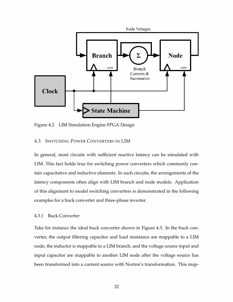
Figure 4.2 LIM Simulation Engine FPGA Design
4.3 SWITCHING POWER CONVERTERS IN LIM
In general, most circuits with sufficient reactive latency can be simulated with
LIM. This fact holds true for switching power converters which commonly con-
tain capacitative and inductive elements. In such circuits, the arrangements of the
latency components often align with LIM branch and node models. Application
of this alignment to model switching converters is demonstrated in the following
examples for a buck converter and three-phase inverter.
4.3.1 Buck Converter
Take for instance the ideal buck converter shown in Figure 4.3. In the buck con-
verter, the output filtering capacitor and load resistance are mappable to a LIM
node, the inductor is mappable to a LIM branch, and the voltage source input and
input capacitor are mappable to another LIM node after the voltage source has
been transformed into a current source with Norton’s transformation. This map-
32

Figure 4.3 Buck Converter
Figure 4.4 Buck Converter LIM Model
ping to LIM components is shown in Figure 4.4. The question arises on how to
handle the switching action of the buck converter with LIM. As seen in previous
discussion on LIM, branch and node models contain respectively a voltage source
E and a current source H which can be arbitrarily altered during simulation. Using
these model sources, the switching action can be handled by altering the values of
H and E in LIM component models in sync with the switching states of a simulated
converter. Applying this idea to the topology of the buck converter with continu-
ous mode switching like seen in Figure 4.5, one can equate during switch-on state
the E term of the inductor branch to the input voltage across the input capacitor
node, and equate the H term of the input capacitor node to the inductor branch
33

(a) Switch On (b) Switch On in LIM
(c) Switch Off (d) Switch Off in LIM
Figure 4.5 Buck Converter Switching Action with LIM Model
current. During the off state of this converter, both H and E are set to zero. By al-
tering H and E terms according to a switching control signal, the switching action
of the converter using LIM is simulated. Other converters, such as the three phase
inverter discussed below, can also be simulated with LIM in similar approach. For
switching behavior in general, H and E terms of switching power converter LIM
models are typically functions of the LIM branch currents and node voltages, with
functions being selected based on switching state of converter.
4.3.2 Three-Phase DC/AC Converter
A three-phase DC-AC converter can be modeled following an approach very sim-
ilar to the one adopted for the buck converter. As can be seen from the converter’s
topology as an inverter, seen in Figure 4.6, the inductors can be mapped to LIM
branch models each, the DC bus capacitance can be modeled as LIM nodes, along
with the output capacitor filter and resistive load. This mapping of the DC/AC
34
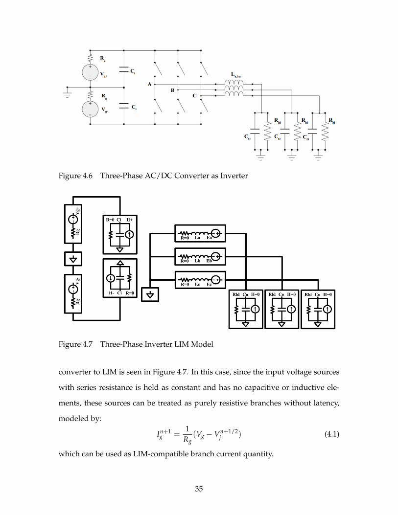
Figure 4.6 Three-Phase AC/DC Converter as Inverter
Figure 4.7 Three-Phase Inverter LIM Model
converter to LIM is seen in Figure 4.7. In this case, since the input voltage sources
with series resistance is held as constant and has no capacitive or inductive ele-
ments, these sources can be treated as purely resistive branches without latency,
modeled by:
In+1g =
1Rg
(Vg −Vn+1/2j ) (4.1)
which can be used as LIM-compatible branch current quantity.
35

To handle the switching action of the three-phase converter, The H terms for the
input node models can be set as functions of the three inductor branch currents,
like so:H+ = −Iasa − Ibsb − Icsc
H− = −Ia sa − Ib sb − Ic sc
(4.2)
where sa through sc and their inversions are the three-phase converter’s modulat-
ing switch control signals per phases a-c, either of value zero or one. Then, for the
E terms of the branch models, their functions can be declared as:
Ea = V+sa + V− sa
Eb = V+sb + V− sb
Ec = V+sc + V− sc
(4.3)
where V+ and V− are teh voltages of the DC bus capacitance nodes, respectively.
To model switching action with deadband interval for this converter, extra
functions are applied for H and E when both switches are off (zero). In this case,
the functions for one of the converter legs is:
H′+ =
0.0 Ia > 0.0
+Ia Ia ≤ 0.0(4.4)
H′− =
0.0 Ia ≤ 0.0
−Ia Ia > 0.0(4.5)
Ea =
V− Ia > 0.0
V+ Ia < 0.0
Va Ia = 0.0
(4.6)
where Va is the output phase voltage. The H′+ from each converter leg are added to
get H+ for complete converter during deadband interval; the same for H−. These
36

(a) Per-Function Method (b) Per-Signal Method
Figure 4.8 Handling Switching Action in LIM Simulation Engine
equations assume that the converter switches have anti-parallel diodes across them
which conduct appropriately during deadband interval.
4.3.3 Converter Switching Behavior Handling on FPGA
Since H and E terms of branches and nodes of switching circuits are generally
functions of branch currents and node voltages, switching behavior can be im-
plemented by feeding results of functions of these current or voltage signals into
a multiplexer whose output feeds into respective H or E input of a LIM entity,
as shown in Figure 4.8(a). Based on the switch state of the converter driven by
a switch control signal, whether continuous or discontinuous mode, appropriate
function can be selected via the multiplexer. Seen in Figure 4.8(b), another way
to handle switching behavior is to have branch current and node voltage signals
switched on or off as input to the H and E functions with multiplexers, based
on the switching signal. In any case, the H and E functions are implemented as
simple dataflow computational expressions which are expected to produce stable
output within the half time step of entity that is recipient of said functions’ results.
Selection of handling method is largely dependent on the converter model to be
simulated with LIM.
37

4.4 FPGA IMPLEMENTATION
This section presents the implementation of the LIM simulation engine in regard
to how computation execution is scheduled for parallelism and how numerical
quantities are stored and processed.
Similar to LB-LMC, the parallelism of FPGAs is exploited by having the equa-
tions of the branch and node entities expressed to be independently from one an-
other through using dedicated computational elements for each equation. Each
entity is designed to operate separately and in parallel to its own type (branch or
node) and only depend on results provided from prior half time steps as input. The
same setup also applies to computational units needed to handle switching action
for both branches and nodes, and branch current summation for node entities. All
operations performed in each half time step update are implemented to finish in
one pass through use of dataflow computational design, requiring two complete
passes for a full time step. For same reasons as in LB-LMC FPGA implementation,
discussed in Section 3.4, fixed point arithmetic is used for all calculations.
4.5 IMPLEMENTATION RESULTS
4.5.1 Setup
To demonstrate implementation of LIM models of power systems, the test models
found in Section 3.5 were re-implemented with the LIM FPGA simulation engine,
using same top-level design as seen in Figure 3.8, with the LB-LMC simulation en-
gine replaced with the LIM one. Again, the same Xilinx VC707 evaluation board
was used in the setup. The simulation engines were developed in C++ with Xil-
inx Vivado VHLS 2015.4 and used 64-bit signed fixed point data types with 35
fractional bits; C++ code found in Appendix B. All engines ran at 40ns time step,
using a 20ns clock source.
38

Table 4.1 Model Error for LIM
Three-PhaseInverter
Single-BusShipboardSystem
Dual-BusShipboardSystem
C++ LIM (%) 0.0266 0.0488 0.0551Traditional RC (%) 1.7394 1.5036 1.4523
4.5.2 Simulation Accuracy and Error
To validate the accuracy of the LIM FPGA simulation engine for each of the test
models, both branch current and node voltage results were logged from RTL-
simulation of each model engine design. Then, the results were compared for
error to offline C++ implementation of the LIM solver running at same time step
with double precision floating type and afterwards compared to traditional resi-
tive companion based simulator running with 400ps time step. Error was com-
puted using (3.3). Results were taken over a 50ms simulation time period after
results have reached steady state for the models. The computed error results are
shown in Table 4.1. Despite going to fixed point type which typically has lower
precision than floating point representation, the FPGA implementation of LIM had
low error well below one percent compared to the C++ implementation with dou-
ble precision float. In comparison to the traditional RC Solver, error was between
1.45 to 1.74 percent, which though not ideal, is reasonable in approximating the
given models analytically.
4.5.3 Demonstration
As was done for the LB-LMC simulation engine, the engine designs for the ship-
board systems were loaded onto the Xilinx VC707 FPGA and analog output from
the board was logged, as seen in Figures 4.9 and 4.10. The output phases of one
of the converters for the single bus system were captured while the switch control
suddenly changed output voltage to higher level. For the dual-bus system, the DC
39
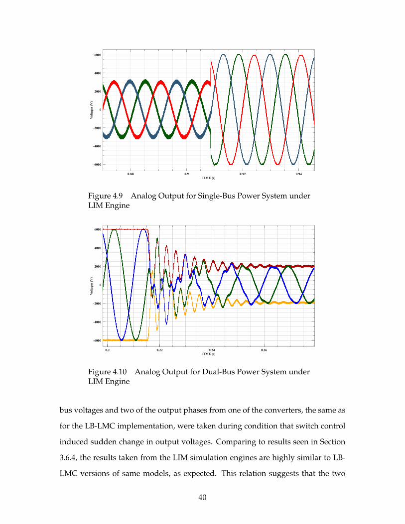
Vol
tage
s (V
)
TIME (s)0.88 0.9 0.92 0.94
-6000
-4000
-2000
0
2000
4000
6000
Figure 4.9 Analog Output for Single-Bus Power System underLIM Engine
Vol
tage
s (V
)
TIME (s)0.2 0.22 0.24 0.26
-6000
-4000
-2000
0
2000
4000
6000
Figure 4.10 Analog Output for Dual-Bus Power System underLIM Engine
bus voltages and two of the output phases from one of the converters, the same as
for the LB-LMC implementation, were taken during condition that switch control
induced sudden change in output voltages. Comparing to results seen in Section
3.6.4, the results taken from the LIM simulation engines are highly similar to LB-
LMC versions of same models, as expected. This relation suggests that the two
40
Vol
tage
(V)
TIME (s)0.25 0.255 0.26 0.265 0.27 0.275 0.28 0.285
-100
-50
0
50
100
Figure 4.11 Deadband Interval Distortion Result
simulation methods, though different in their implementation and structure, are
analytically equivalent within reasonable boundaries, at least for these test mod-
els.
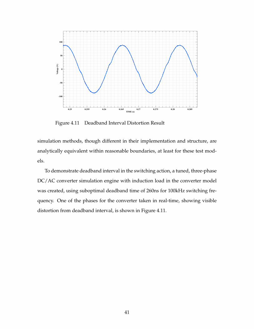
To demonstrate deadband interval in the switching action, a tuned, three-phase
DC/AC converter simulation engine with induction load in the converter model
was created, using suboptimal deadband time of 260ns for 100kHz switching fre-
quency. One of the phases for the converter taken in real-time, showing visible
distortion from deadband interval, is shown in Figure 4.11.
41

CHAPTER 5
SCALABILITY ANALYSIS
One of the important aspects to choosing a simulation method for FPGA imple-
mentation is how the method scales on such hardware as the size and complexity
of the simulated system grows. One element of scalability is computational delay
which affects the size of time step usable. Should a simulation method require
quadratic or even linear scaling of delay as the model grows, the time step achiev-
able for large systems may become too great to precisely capture model behavior
in real-time during simulation. As such, it is desirable to have computational de-
lay scale sublinearly or stay constant as a model grows in size. Another element
is amount of resources required to realize the computations. To acheive low com-
putational delay in the nanosecond range, it is required to exploit parallelism on
FPGAs to maximize number of computations in a given time. This parallelism
is achieved by giving each computation of an equation or expression in a system
model dedicated resources on the given FPGA. Therefore, as a model grows in
size, so does the resources needed to simulate the model. Since all FPGAs have
finite amount of resources to give for a simulation engine of a given method, un-
derstanding how resources scales with model size is important to ensure larger
system models can fit on a choosen FPGA device. In this chapter, the computation
delay and resource usage of LB-LMC and LIM are analyzed at element level, and
the methods are compared within this regard using real-world results taken from
a model of increasing size.
42

5.1 LB-LMC
This section discusses the scalability of the FPGA implementation of the LB-LMC
solver as model size increases, in terms of achievable time step (computation de-
lay), clock cycle latency, and FPGA resource usage.
5.1.1 Components
The number of operations required to compute the internal states and source con-
tributions of a component is largely dependent on the component model and in-
tegration method used. However, the total number of operations required for a
collection of components of same model and type will scale linearly as more com-
ponents of same type are instanced in a simulation engine. This linear scaling
of operations also applies to resource usage as each operation of same type uses
similar amount of resources. Though resource usage will increase linearly with
number of components, the computational delay for all components of same type
to perform their operations will stay constant due to the parallel operation of said
components.
5.1.2 Dataflow System Solver
As the size of a modeled, independent system or subsystem grows to n solutions,
the number of operations required for the solver grows by an order of 2, with num-
ber of multiplications needed being n2, and additions being n(n− 1). If each oper-
ation type (multiplication or addition) is mapped to unchanging FPGA resources
without any FPGA synthesis optimizations, the amount of resources needed for
the dataflow will also grow by an order of 2 as well. Due to this growth of re-
sources, the system solver can act as a bottleneck that determines how large of a
model and its simulation engine can fit on a given FPGA device. To reduce num-
ber of operations and FPGA resources in the dataflow system solver, the modeled
43

system is broken up into subsystems where possible and each subsystem is given
its own solver with reduced size n.
The computation delay of the dataflow system solver will grow sublinearly
as a model size increases due to the multiplication and addition operations per-
formed in parallel, dataflow manner on FPGA hardware. This scaling is unlike
a traditional CPU or DSP whose computational time or delay for the solving of
these system equations will grow with an order of 2 as the number of solutions
increases, due to performing all operations sequentially.
5.1.3 Multi-cycle System Solver
The number of operations implemented in hardware of the multi-cycle system
solver is inversely proportional to the number of iterations selected for the solver
to compute a solution. Resource usage will scale similarly, though extra resources
are required to enable multi-iteration computation and pipelining. Computational
time of the system solver is a function of cycles needed for the solver to reach so-
lution, where the time is a product of the number of cycles, including extra cycles
for pipeline priming, and the clock period used.
5.1.4 Simulation Engine Time Step and Computation Delay
The time step usable for the simulation engine is dependent on the computational
delay and latency of the components and system solver. With the dataflow system
solver, the time step must be greater than the sum of computational delay required
for the slowest component entity type and the delay needed for the system solver
to have all solutions computed and stabilized; this sum being the total computa-
tional delay of the simulation engine:
∆t > tsolver + tcomp_delay (5.1)
44

For larger system models, it is expected that the simulation engine computational
delay will be dominated by the system solver delay as component model entities’
delays do not grow with system size and expected to typically be small in compu-
tational complexity. To greatly reduce system solver delay, and reduce time step,
subsystem decomposition can be used within the system solver as noted before.
In the case of using a multi-cycle system solver, the system solver will again
greatly influence the time step for the simulation engine due the solver’s need for
multiple cycle latency needed to reach the system solution each time step. The
computation time of the simulation engine will be the number of cycles needed
for system solver to reach solution times the clock period used to clock the solver,
plus the delay needed for the slowest type of component entities to perform their
operations. From this relation, the time step will have to be:
∆t > nsol_cyclestclk + tcomp_delay (5.2)
Reduction of multi-cycle system solver latency, and in turn the time step, can be
achieved through reducing the number of cycles needed to compute the solution
through performing more system solution equation operations per cycle, or to an
lesser effect, reduce the clock period. In either case, the tradeoff is higher usage of
FPGA resources.
5.2 LIM
This section discusses the scalability of the FPGA implementation of the LIM solver
as model size increases, in terms of achievable time step (computation delay), clock
cycle latency, and FPGA resource usage.
45

5.2.1 Entities
Due to the fixed nature of the component entities in LIM, the number of opera-
tions within a branch and a node component will stay constant, regardless of the
system model and its size. Therefore, the total number of operations needed for a
given number of branches and nodes in a model grows linearly with the model in
question. Since resources realize these operations, they will increase at same scale
as said operations. Though resource usage grows linearly, computational delays
for both branch and node entities shall stay relatively constant due to entities of
same type all updated in parallel.
5.2.2 Simulation Engine Time Step and Computation Delay
Due to the leapfrog approach used to handle the simulation flow of the LIM en-
gine, and using the same clock period for branch updates and node updates, the
achievable time step for a given system model will always be greater than or equal
to twice the said clock period, expressed as:
∆t ≥ 2tclk (5.3)
This clock period tclk is a function of how long the engine takes to compute the
longest half time step update period, whether for branch updates or node updates.
The computation time for the update periods is influenced by switching action
computations performed under either component update time for converter sim-
ulation and by computational time needed to sum branch currents together for a
given node component during node update period; on top of computational time
for branches and nodes themselves. For branch updates, the compute time will be:
tbranch = tswitch_compute + tupdate (5.4)
and for the node updates:
tnode = tswitch‖sum_compute + tupdate (5.5)
46
, where tswitch‖sum_compute is the time needed to perform the longest current sum-
mation and switching action calculations in parallel. From these computational
times, the time step is determined by:
∆t ≥ 2MAX(tbranch, tnode) (5.6)
5.3 EVALUATION
In this section, the scalability evaluation of each method implementation is pre-
sented. To perform evaluation, a single-bus power system was used as the test
case, where the size of the model was increased by cascading converters onto the
DC bus incrementally. This model was implemented under each method on the
FPGA evaluation board and the estimated resource usage and computational de-
lay reported by Xilinx Vivado for each incrementation.
5.3.1 Setup
As a test case for the scalability evaluation of both LIM and LB-LMC FPGA imple-
mentations, the signal bus system model shown in Figure 5.1 was developed under
both methods with increasing N number of converters and their corresponding ca-
ble segments and loads. For each size of the model, the simulation engine of the
model under each simulation method was synthesized and implemented under
Xilinx Vivado 2015.4 for Xilinx Virtex-7 485t VC707 evaluation board and the tim-
ing and resource usage report generated by said tool was recorded; only the results
of the simulation engine and not of any peripheral entities (switch control, analog
output) were noted. The size of the model was increased by three converters for
every run after the first converter, until the simulation engine of the model could
longer fit, either by running out of resources or route paths on the FPGA. The
models were synthesized for the fastest clock period (and time step) achievable
for a given model size; if a model FPGA implementation could not meet desired
47

Figure 5.1 Scalability Test Model
timing, the clock period used for the design was increased by 5ns and the design
was re-implemented for the new timing. The LB-LMC engine in the test was run
in single pass per time step operation and required 72-bit fixed point for precise
computation; the LIM engine requires only 64-bit fixed point to achieve similar
accuracy as the LB-LMC setup. For N number of converters included in the model
under LB-LMC, the number of inductor models for the cable line increased by 2N
and the number of capacitors for the converter output filtering increased by 3N.
The number of circuit nodes in the model increased by 7N + 2. Under LIM, both
the branch entity and node entity amount increased by 5N.
5.3.2 LIM Results
The LIM simulation engine scalability results are shown in Figure 5.2 and Table
5.1. The computational delay is the estimated longest time needed by the LIM
engine to update one half time step, either the branch half or the node half. As
expected, the results show that LIM is very scalable on an FPGA, having linear
increase in resources as converters are added to the model, with 140 DSPs and ap-
proximately 10000 LUTs needed for every converter and corresponding circuit ele-
ments; this usage allowing up to 17 converter models to be instanced on the FPGA.
48

Table 5.1 LIM Scalability Results
N Computational Delay (ns) Time Step (ns) LUTs DSPs1 18.068 40 10149 1404 18.281 40 40478 5607 19.307 40 70939 98010 19.271 40 101341 140013 19.935 40 131792 182016 19.963 40 162634 224017 19.809 40 172903 2380
LUT
N Converters0 1 2 3 4 5 6 7 8 9 10 11 12 13 14 15 16 17
20000400006000080000
100000120000140000160000
Com
puta
tiona
l Del
ay (n
s)
N Converters0 1 2 3 4 5 6 7 8 9 10 11 12 13 14 15 16 17
18.5
19
19.5
20
DSP
N Converters0 1 2 3 4 5 6 7 8 9 10 11 12 13 14 15 16 17
500
1000
1500
2000
Figure 5.2 Plot of LIM Scalability Results
The computational delay stayed relatively constant for every N of converters in-
cluded, with delay approximately between 18 and 20 ns, allowing each model size
examined to use a 40ns time step. It is suspected that the variation in delay is
primarily from routing delays between resources on the FPGA, these delays in-
creasing as resource utilization on the FPGA becomes more congested.
49

Table 5.2 LB-LMC Scalability Results
N Computational Delay (ns) Time Step (ns) LUTs DSPs1 43.184 45 8862 2644 44.594 45 39475 9637 44.503 45 69347 165710 45.738 45 98988 235510 48.478 50 105735 2354
5.3.3 LB-LMC Results
The scalability results for the LB-LMC simulation engine are presented in Figure
5.3 and Table 5.2. As predicted, the resource usage of LB-LMC on FPGA approx-
imately scaled linearly, with LUTs increasing to additional 9925 on average for
every new converter added to the model with corresponding elements, and DSPs
increasing by 236 on average for every new converter segment cascaded to the
model. However, the amount of resources needed for each tested size of the model
was higher than that of the LIM engine usage, limiting number of converters to a
count of 10. It is expected that the extra resource usage is from needing to use
72-bit fixed point data sizes to keep result accuracy reasonable, which is higher
than 64-bit size used by LIM model for similar accuracy. Use of larger word size
requires more resources to perform computations. Furthermore, LB-LMC engine
uses a system solver that LIM does not have, this solver growing larger as the
model size increases and serving as extra overhead to the LB-LMC engine. The
computational delay scaled sublinearly as expected like LIM, but minimum time
step allowed by the delay was 5ns greater than LIM for same model. Moreover,
the computational delay grew at quicker rate than with LIM, causing the model
engine to fail desired timing with 10 converters and needing to raise time step
to 50ns for this size. At 50ns time step, the model engine needed 48.5ns to reach
solutions every time step, higher than 44.5 and 45.7 ns from other runs, though
the larger increase is likely from routing delays and effort made by Xilinx Vivado
50

LUT
N Converters0 1 2 3 4 5 6 7 8 9 10
20000
40000
60000
80000
100000
Com
puta
tiona
l Del
ay (n
s)
N Converters0 1 2 3 4 5 6 7 8 9 10
43.5
44
44.5
45
45.5
DSP
N Converters0 1 2 3 4 5 6 7 8 9 10
500
1000
1500
2000
Figure 5.3 Plot of LB-LMC Scalability Results
place-and-route tool to meet given 50ns time step. In any case, the greater increase
in computational delay is expected to stem from system equations in the system
solver increasing in length as more components and nodes are added to the test
model. Though the equations come out to be dataflow computional units where
multiplication operations are performed in parallel, the summuation of all multi-
plication results still needs to be accumulated to acquire the final result for a given
node voltage. This summuation, using dual input addition units for each add, is
a sequential process where the result of two additions need to be added together
and so forth. As a sequential process, computational delay is expected to increase.
51

CHAPTER 6
MODELING AND IMPLEMENTATION DISCUSSION
In creating a power system model for FPGA implementation with a given simula-
tion method, it is important to understand the limitations and challenges in getting
such models to work in such a setup. Limitations can include, though not limited
to, whether a system model can be instanced in a given method, if possible, with-
out significant network transformations and modifications, or whether a model
can be executed without becoming numerical instable or inaccurate for given time
step or data word size. Other challenges can involve the process of implementing
the model on FPGA once said model is created, such as pre-computing system ma-
trices and developing solvers. In this chapter, these limitations and challenges for
creating power system models for the FPGA implementations of LB-LMC method
and LIM are discussed and compared.
6.1 LB-LMC MODELING ON FPGA
A major limitation of the FPGA implementation of LB-LMC is the system solver.
Unlike LIM, LB-LMC requires a system solver that is separate from the circuit com-
ponent entities that make up a given power system model. This system solver de-
pends on a pre-computed conductance matrix G that describes the conductances
of the system network. For every model to be simulated, the conductance ma-
trix, and its inversion G−1, must be computed offline from the LB-LMC simulation
engine. As such, if any parameter of the model needs to be altered, say for exam-
ple the load for a power converter, the matrix must be recomputed every time and
52

the FPGA implementation needs to be re-synthesized as well; a lengthy process for
large system models using existing FPGA synthesis tools. The re-computation and
re-synthesis is also required if the time step is changed as the time step is included
in calculations of conductances for components with latency, such as capacitors
and inductors; this prevents the possibilities of effectively changing the time step
of a simulation after a model has been loaded onto a given FPGA.
Beyond the conductance matrix, the system solver also requires modifications
or recreation for different or changing system topologies before a model can be
synthesized for FPGA execution. As the system topology is altered, the linear
equations that model the system will also change, requiring modeling equations
in the system solver to be altered. For instance, if new components are added to
a model and linked to nodes, the sub-solver of the system solver that accumulates
the b vector of the system will need to modified to take the source contributions
from the new components. Furthermore, should non-independent elements be
added to a model that instances new nodes in the system network, the size and
number of equations as seen in (3.2) will need to be expanded as well.
Despite the issue with the conductance matrix and system solver, LB-LMC is
requires little to no modification to a given system model to be implemented in it.
Unlike LIM, LB-LMC can support most circuit elements and topologies. This sup-
port lies in LB-LMC method’s use of linear equations to model and solve system
network models, similar to how Resistive Companion (RC) method works which
is used in commercial simulation tools such as SPICE. Moreover, due to LB-LMC
method’s roots from RC method, LB-LMC supports a wide variety of integration
methods, implicit/explicit or mixed, to approximate state equations for latency in-
ducing circuit elements to enable desired modeling stability and accuracy for given
time step size. These benefits allow LB-LMC to be highly versatile and robust for
simulating virtually any power system to be evaluated.
53
6.2 LIM MODELING ON FPGA
Despite proving to be highly scalable for real-time simulation on FPGA as noted
in Chapter 5, LIM does suffer from the issue of requiring rigid topology structure
for system models which LB-LMC lacks. In traditional LIM, branches must always
be composed of inductor with optional series resistance and voltage source, and
nodes must comprise of a capacitor to ground with optional parallel conductance
and current source. However, many electrical networks do not fit this structure,
such as having capacitors serving as a branch between two nodes. Ideally, most
systems can be made to fit LIM structure through network transformations, exam-
ples including but not limited to Thevenin and Norton transformations, but some
topologies would require overly extensive modifications to be practical. Then, for
branches and nodes in a system that contain no latency elements (sources and re-
sistances), latency must be artificially inserted into a model to fit LIM structure,
thereby making the model less of an accurate approximation of a given system.
For LIM to be more versatile, LIM will need to be expanded with new compati-
ble branch and node entities to enable less rigid topology requirements; such as
branch capacitors, node inductors, and non-latency elements.
Along with topology issues, LIM is sensitive to numerical stability for larger
time steps or small latencies. Traditional LIM uses an explicit integration to ap-
proximate the state equations of the branches and nodes, as seen in (2.7) and (2.9).
From this use of explicit integration, should the latency (capacitance or inductance)
be significantly smaller than for a given time step, computed solutions for each
half time step in LIM can become unstable, causing the model to fail. Though the
nanosecond range time steps achievable with LIM on FPGA allow usage of small
capacitances and inductances in real-time, instability can arise when attempting to
model detailed system models that incorporate all parasitic effects that often are
minuscule.
54

Though LIM is inflexible in system topology and latency inclusion, this method
is more robust in FPGA implementation compared to LB-LMC. Not needing a sys-
tem solver, or related conductance matrix, like LB-LMC, LIM only requires enti-
ties for each branch and node for a model to be instanced and then to link them
together. Without a large, central element needing to change with the model, com-
ponent parameters can be more readily altered, including time step. This setup
even enables the possibility of changing parameters and time step after a model
design has been synthesized and loaded onto a FPGA through replacing the cur-
rently used parameter constants with configurable registers or block RAM units on
a FPGA. However, should the topology need to change though, the model design
will still need to be re-synthesized again.
55

CHAPTER 7
FUTURE WORK
While the present work on the LB-LMC and LIM implementations on FPGA have
brought high-fidelity and scalable tools to simulate power systems, much work
can be done to take the implementations further to improve practical usefulness
and robustness of said implementations. Currently, the FPGA simulation engines
have to be hand-developed for every system model to simulate. For larger models,
this development can become tedious and highly error-prone, especially if multi-
ple models have to be instanced. Instead, further work can be done to automati-
cally generate the RTL code for the simulation engines from a given power system
model. This work can be done through creating software tools which take the
netlist and parameters of a system model and then generate the appropriate code
of the simulation engine for the model that can be synthesized for FPGA execution.
Other work that can be performed is expanding development of the multi-pass
execution for the LB-LMC simulation engines. In present state, the LB-LMC sim-
ulation engine with multi-pass execution gains greatest resource usage reduction
when the sub-system solver execution is looped, though usage reduction is not as
great as expected. Other attempts of implementing multi-pass execution, includ-
ing looping the solving of each linear equation in the system solver, have caused
resource usage increases beyond using single pass execution. Efforts can be made
to reduce resource usage further for multi-pass execution while still maintaining
adequate time steps for high frequency switching converter modeling. Moreover,
other work can be explored to incorporate pipelined floating-point arithmetic op-
56

erations into the multi-pass execution to dramatically improve simulation preci-
sion and error over using fixed-point arithmetic.
One element that can be improved is the limited versatility of the LIM FPGA
implementation. Currently, only inductor branches and capacitor nodes have been
implemented as entities in the LIM simulation engine design. While these two en-
tities can model a wide variety of power electronic systems, many other systems
cannot be modeled with only these two. For instance, three-phase wye or delta
configuration of inductors, commonly seen in power loads, cannot be modeled
with the branch entities because the configuration requires inductors to be con-
nected together without nodes entities in-between. Moreover, power converters in
full bridge topology that incorporate filter capacitors between switch legs will re-
quire a branch capacitor. Other LIM-compatible components, including branch ca-
pacitors, node inductors, and transformer elements that are mentioned in [12], can
be implemented in the FPGA simulation engine design to enable further amount
of power electronic systems to be modeled.
Another thing that can be taken further is optimizing the FPGA simulation
engines for reduced resource usage and computational delay. While the scala-
bility of the two methods on FPGA are admirable, the size of the models is still
limited by the amount of resources available on FPGAs, keeping potential for ex-
tensively sized power system models from existing. Significant reduction of re-
sources, through changing data word size and re-expressing model equations for
less operations, can allow larger models to be simulated on FPGA with LB-LMC
or LIM. Decrease in computational delay for simulation methods would be also
be something to explore in future work to improve scalability of LB-LMC and to
reduce time steps below 40ns.
Finally, work can be taken further to enable hardware-in-the-loop (HIL) and
power HIL (PHIL) simulation with the simulation engine FPGA implementations
57
for both methods. The current simulation platform implementation presented in
this work could be expanded to allow simulated power electronic systems to in-
teract with physical elements such as closed-loop controller units, AC machines,
and more. With the real-time execution of the developed simulation engines and
availability of analog IO boards, the potential for HIL simulation for testing with
real systems and external closed-loop power system control exists. However, HIL
simulation with the engines was not fully explored due to time constraints. This
situation can be remedied in future iterations of this work.
58

CHAPTER 8
CONCLUSION
The demand in scalable, system-level, real-time simulation for power electronic
systems has increased in recent years. FPGA implementations of existing latency-
based simulation methods, LB-LMC and LIM, were developed, analyzed, and
compared to see if they can meet these demands and provide new benefits to high
fidelity, real-time simulation. The LB-LMC method was implemented on a Virtex-7
FPGA, with various component entities solving themselves in parallel before hav-
ing the system solver linearly compute total system solution in single or multiple
pass execution per time step. LIM was realized on same FPGA, operating in two-
pass, leapfrog execution where all branches update in parallel together during first
half time step and then all nodes simultaneously update in second half time step.
Switching action of power converters were modeled with altering the voltage and
current source terms of the LIM entities during respective half time step update
period. After analysis, these two methods implemented on FPGA proved to be
highly scalable. The LB-LMC method was able to simulate power systems with
up to ten converters, running with time steps between 45 to 50ns. Likewise, LIM
implementation was able to simulate systems with up to seventeen converters,
running with a time step of 40ns and below for all test cases. Both methods scaled
in resource usage linearly for every converter incorporated into the model, though
LIM had lesser increase in resources as model size increased when compared to
LB-LMC method. Despite the scalability of LIM implementation on FPGA, LIM
does suffers from limited versatility of possible system models and numerical in-
59

stability when latency is too small or time steps are too large for given system
dynamics. On the other hand, the LB-LMC method, while suffering from need of
a costly system solver that needs to be altered for every system model, is capable
of stably modeling a vastly larger variety of power electronic system models with
little to no modification to said models due to roots in the widely proven resistive
companion method. With the two implementations, new groundwork is made for
the progression of system-level, real-time simulation of power electronic systems.
60

REFERENCES
[1] L. Bin, X. Wu, H. Figueroa, and A. Monti, “A low-cost real-time hardware-in-the-loop testing approach of power electronics controls,” IEEE Trans. Ind.Electron., vol. 54, pp. 919–931, Feb. 2007.
[2] L. Yunwei, D. Vilathgamuwa, and L. P. Chiang, “Design, analysis, and real-time testing of a controller for multibus microgrid system,” IEEE Trans. PowerElectron., vol. 19, pp. 1195–1204, May 2005.
[3] Z. Ivanovic, E. Adžic, M. Vekic, S. Grabic, N. Celanovic, and V. Katic, “Hilevaluation of power flow control strategies for energy storage connected tosmart grid under unbalanced conditions,” IEEE Trans. Power Electron., vol. 27,pp. 4699–4710, Nov. 2012.
[4] M. Matar and R. R. Iravani, “FPGA implementation of the power electronicconverter model for real-time simulation of electromagnetic transients,” IEEETrans. Power Del., vol. 25, pp. 852–860, Feb. 2010.
[5] N. R. Tavana and V. Dinavahi, “Real-time nonlinear magnetic equivalent cir-cuit model of induction machine on FPGA for hardware-in-the-loop simula-tion,” IEEE Trans. Energy Convers., vol. 31, pp. 520–530, Feb. 2016.
[6] J. Liu and V. Dinavahi, “A real-time nonlinear hysteretic power transformertransient model on FPGA,” IEEE Trans. Ind. Electron., vol. 61, pp. 1254–1260,Jul. 2014.
[7] H. Saad, T. Ould-Bachir, J. Mahseredjian, C. Dufour, S. Dennetiere, andS. Nguefeu, “Real-time simulation of MMCs using CPU and FPGA,” IEEETrans. Power Electron., vol. 30, pp. 259–267, Jan. 2015.
[8] J. Jin-Hong, K. Jong-Yul, K. Hak-Man, K. Seul-Ki, C. Changhee, K. Jang-Mok,A. Jong-Bo, and N. Keo-Yamg, “Development of hardware inthe-loop simu-lation system for testing operation and control functions of microgrid,” IEEETrans. Power Electron., vol. 25, pp. 2919–2929, Dec. 2010.
61
[9] V. Jalili-Marandi, L. Pak, and V. Dinavahi, “Real-time simulation of grid-connected wind farms using physical aggregation,” IEEE Trans. Ind. Electron.,vol. 57, pp. 3010–3021, Sep. 2010.
[10] W. Li, G. Joós, and J. Bélanger, “Real-time simulation of a wind turbine gen-erator coupled with a battery supercapacitor energy storage system,” IEEETrans. Ind. Electron., vol. 57, pp. 1137–1145, Apr. 2010.
[11] A. Benigni and A. Monti, “A parallel approach to real-time simulation ofpower electronics systems,” IEEE Trans. Power Electron., vol. 30, pp. 5192–5206, Sep. 2015.
[12] J. E. Schutt-Aine, “Latency insertion method (LIM) for the fast transient sim-ulation of large networks,” IEEE Trans. Circuits Syst. I, vol. 48, pp. 81–89, Jan.2001.
62

APPENDIX A
LB-LMC ENGINE HLS C++ CODE
A.1 CAPACITOR ENTITY
1 # include " Capacitor .hpp"23 Capacitor :: Capacitor ( NumType dt , NumType cap)4 : dt(dt), cap(cap), hoc2( NumType (2.0)*cap/dt)5 , epos_past (0.0) , eneg_past (0.0) ,delta_v (0.0) ,delta_v_past (0.0)6 , current (0.0) ,current_eq (0.0) ,current_past (0.0) ,current_eq_past
(0.0)7 {}89 void Capacitor :: operator ()( NumType epos , NumType eneg , NumType *
bout)10 {11 # pragma HLS inline1213 # pragma HLS latency min =0 max =01415 // register past values16 epos_past = epos;17 eneg_past = eneg;18 current_past = current ;19 current_eq_past = current_eq ;20 delta_v_past = delta_v ;2122 delta_v = AddSubType ( epos_past ) - AddSubType ( eneg_past );2324 current = (hoc2)*( delta_v ) - ( current_eq_past );2526 current_eq = ( current ) + (hoc2)*( delta_v );2728 *bout = current_eq ;29 }
63

A.2 INDUCTOR ENTITY
1 # include " Inductor .hpp"23 Inductor :: Inductor ( NumType dt , NumType ind)4 : dt(dt), ind(ind), hol2(dt/ NumType (2.0)/ind)5 , epos_past (0.0) , eneg_past (0.0) ,delta_v (0.0) ,delta_v_past (0.0)6 , current (0.0) ,current_eq (0.0) ,current_past (0.0) ,current_eq_past
(0.0)7 {}89 void Inductor :: operator ()( NumType epos , NumType eneg , NumType *
bout)10 {11 # pragma HLS inline1213 # pragma HLS latency min =0 max =01415 // register past values16 epos_past = epos;17 eneg_past = eneg;18 current_past = current ;19 current_eq_past = current_eq ;20 delta_v_past = delta_v ;2122 delta_v = AddSubType ( epos_past ) - AddSubType ( eneg_past );2324 current = hol2* delta_v - current_eq_past ;2526 current_eq = -current - hol2* delta_v ;2728 *bout = current_eq ;29 }
A.3 THREE PHASE HALF-BRIDGE CONVERTER ENTITY
1 # include " ThreePhaseHBConverter .hpp"23 ThreePhaseHBConverter :: ThreePhaseHBConverter ( NumType dt , NumType
cap , NumType ind , NumType res)4 : dt(dt), cap(cap), ind(ind), res(res), hoc(dt/cap), hol(dt/ind),
cap_conduct (10000.0)5 ,vc1 (0.0) ,vc2 (0.0) ,il1 (0.0) ,il2 (0.0) ,il3 (0.0) ,ipos (0.0) ,ineg
(0.0)6 ,epos_past (0.0) ,eneg_past (0.0) ,eout1_past (0.0) ,eout2_past (0.0) ,
eout3_past (0.0)7 ,il1_past (0.0) ,il2_past (0.0) ,il3_past (0.0) ,vc1_past (0.0) ,
vc2_past (0.0)
64

8 ,sw1(false),sw2(false),sw3(false)9 {}
1011 void ThreePhaseHBConverter :: operator ()( NumType epos , NumType eneg
, NumType eout1 , NumType eout2 , NumType eout3 ,12 NumType * bpos , NumType * bneg , NumType * bout1 , NumType * bout2 ,
NumType * bout3 ,13 bool sw_ctrl1 , bool sw_ctrl2 , bool sw_ctrl3 )14 {15 # pragma HLS inline1617 # pragma HLS latency min =0 max =01819 epos_past = epos;20 eneg_past = eneg;21 eout1_past = eout1;22 eout2_past = eout2;23 eout3_past = eout3;24 il1_past = il1;25 il2_past = il2;26 il3_past = il3;27 vc1_past = vc1;28 vc2_past = vc2;29 sw1 = sw_ctrl1 ;30 sw2 = sw_ctrl2 ;31 sw3 = sw_ctrl3 ;3233 AddSubType a1 , a2 , a3 , b1 , b2 , b3 , a, b, c;3435 if(sw1)36 {37 a1 = il1_past ;38 b1 = 0.0;39 a = vc1_past ;40 }41 else42 {43 a1 = 0.0;44 b1 = il1_past ;45 a = vc2_past ;46 }4748 if(sw2)49 {50 a2 = il2_past ;51 b2 = 0.0;52 b = vc1_past ;53 }54 else55 {56 a2 = 0.0;57 b2 = il2_past ;58 b = vc2_past ;59 }
65
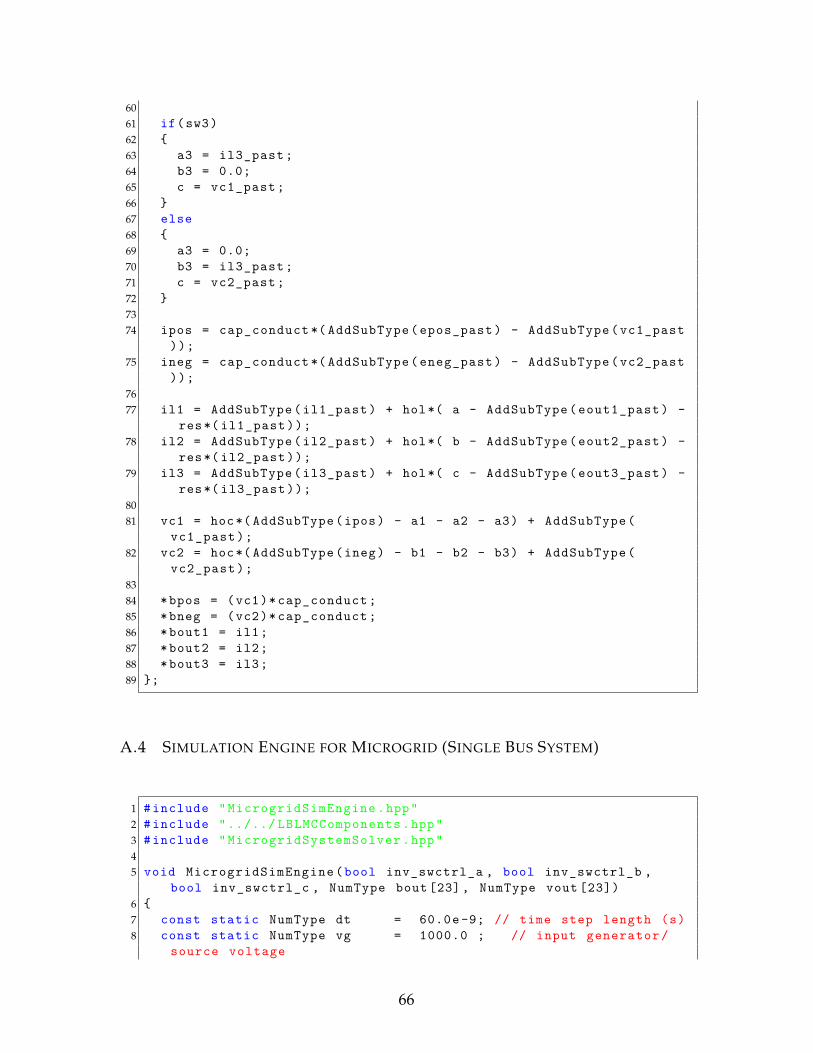
6061 if(sw3)62 {63 a3 = il3_past ;64 b3 = 0.0;65 c = vc1_past ;66 }67 else68 {69 a3 = 0.0;70 b3 = il3_past ;71 c = vc2_past ;72 }7374 ipos = cap_conduct *( AddSubType ( epos_past ) - AddSubType ( vc1_past
));75 ineg = cap_conduct *( AddSubType ( eneg_past ) - AddSubType ( vc2_past
));7677 il1 = AddSubType ( il1_past ) + hol *( a - AddSubType ( eout1_past ) -
res *( il1_past ));78 il2 = AddSubType ( il2_past ) + hol *( b - AddSubType ( eout2_past ) -
res *( il2_past ));79 il3 = AddSubType ( il3_past ) + hol *( c - AddSubType ( eout3_past ) -
res *( il3_past ));8081 vc1 = hoc *( AddSubType (ipos) - a1 - a2 - a3) + AddSubType (
vc1_past );82 vc2 = hoc *( AddSubType (ineg) - b1 - b2 - b3) + AddSubType (
vc2_past );8384 *bpos = (vc1)* cap_conduct ;85 *bneg = (vc2)* cap_conduct ;86 *bout1 = il1;87 *bout2 = il2;88 *bout3 = il3;89 };
A.4 SIMULATION ENGINE FOR MICROGRID (SINGLE BUS SYSTEM)
1 # include " MicrogridSimEngine .hpp"2 # include " ../../ LBLMCComponents .hpp"3 # include " MicrogridSystemSolver .hpp"45 void MicrogridSimEngine (bool inv_swctrl_a , bool inv_swctrl_b ,
bool inv_swctrl_c , NumType bout [23] , NumType vout [23])6 {7 const static NumType dt = 60.0e -9; // time step length (s)8 const static NumType vg = 1000.0 ; // input generator /
source voltage
66

9 const static NumType rg = 0.001 ; // input generator /source series resistance
10 const static NumType line_l = 0.0001 ; // line/businductance per segment
11 const static NumType line_r = 0.1 ; // line/bus seriesresistance per segment
12 const static NumType inv_cin = 0.001 ; // input buscapacitance of 3p inverters
13 const static NumType inv_cfilt = 1.0e-6 ; // outputcapacitance of 3p inverters
14 const static NumType inv_lfilt = 0.0001 ; // outputinductance of 3p inverters
15 const static NumType inv_rfilt = 0.0 ; // output seriesresistance of 3p inverters
16 const static NumType load_r = 10.0 ; // load resistance ofthe inverters
1718 // ///////////////////////////////////////////19 // signals2021 NumType inv_b [15];22 NumType cap_b [9];23 NumType ind_b [6];24 NumType srcv_b [2];2526 static NumType v[23]; // zero indexed , so v[0] = v12728 // ///////////////////////////////////////////29 // components3031 srcv_b [0] = vg/rg;32 srcv_b [1] = vg/rg;3334 static Inductor l01(dt , line_l );35 static Inductor l02(dt , line_l );36 static Inductor l03(dt , line_l );37 static Inductor l04(dt , line_l );38 static Inductor l05(dt , line_l );39 static Inductor l06(dt , line_l );4041 static ThreePhaseHBConverter inv1(dt , inv_cin , inv_lfilt ,
inv_rfilt );42 static ThreePhaseHBConverter inv2(dt , inv_cin , inv_lfilt ,
inv_rfilt );43 static ThreePhaseHBConverter inv3(dt , inv_cin , inv_lfilt ,
inv_rfilt );4445 static Capacitor c01(dt , inv_cfilt );46 static Capacitor c02(dt , inv_cfilt );47 static Capacitor c03(dt , inv_cfilt );48 static Capacitor c04(dt , inv_cfilt );49 static Capacitor c05(dt , inv_cfilt );50 static Capacitor c06(dt , inv_cfilt );51 static Capacitor c07(dt , inv_cfilt );
67
52 static Capacitor c08(dt , inv_cfilt );53 static Capacitor c09(dt , inv_cfilt );5455 // ///////////////////////////////////////////56 // simulation loop5758 l01(v[ 0],v[ 1], ind_b+ 0);59 l02(v[ 2],v[ 3], ind_b+ 1);60 l03(v[ 4],v[ 5], ind_b+ 2);61 l04(v[ 7],v[ 8], ind_b+ 3);62 l05(v[ 9],v[10] , ind_b+ 4);63 l06(v[11] ,v[12] , ind_b+ 5);6465 inv1(v[ 2],v[ 9],v[14] ,v[15] ,v[16] , inv_b+ 0,inv_b+ 1,inv_b+ 2,
inv_b+ 3,inv_b+ 4, inv_swctrl_a , inv_swctrl_b , inv_swctrl_c );66 inv2(v[ 4],v[11] ,v[17] ,v[18] ,v[19] , inv_b+ 5,inv_b+ 6,inv_b+ 7,
inv_b+ 8,inv_b+ 9, inv_swctrl_a , inv_swctrl_b , inv_swctrl_c );67 inv3(v[ 6],v[13] ,v[20] ,v[21] ,v[22] , inv_b +10, inv_b +11, inv_b +12,
inv_b +13, inv_b +14, inv_swctrl_a , inv_swctrl_b , inv_swctrl_c );6869 c01(v[14] , 0.0, cap_b +0);70 c02(v[15] , 0.0, cap_b +1);71 c03(v[16] , 0.0, cap_b +2);72 c04(v[17] , 0.0, cap_b +3);73 c05(v[18] , 0.0, cap_b +4);74 c06(v[19] , 0.0, cap_b +5);75 c07(v[20] , 0.0, cap_b +6);76 c08(v[21] , 0.0, cap_b +7);77 c09(v[22] , 0.0, cap_b +8);7879 MicrogridSystemSolver (inv_b , cap_b , ind_b , srcv_b , bout , v);8081 // output solution vector82 for(int i = 0; i <23;i++)83 {84 # pragma HLS UNROLL8586 vout[i] = v[i];87 }88 }
A.5 SYSTEM SOLVER FOR MICROGRID (SINGLE BUS SYSTEM)
1 # include " MicrogridSystemSolver .hpp"23 void MicrogridSystemSolver ( NumType inv_b [15] , NumType cap_b [9],
NumType ind_b [6], NumType srcv_b [2], NumType bout [23] ,NumType v[23])
4 {5 # pragma HLS INTERFACE ap_none port=inv_b
68

6 # pragma HLS ARRAY_PARTITION variable =inv_b dim =17 # pragma HLS INTERFACE ap_none port=cap_b8 # pragma HLS ARRAY_PARTITION variable =cap_b dim =19 # pragma HLS INTERFACE ap_none port=ind_b
10 # pragma HLS ARRAY_PARTITION variable =ind_b dim =111 # pragma HLS INTERFACE ap_none port= srcv_b12 # pragma HLS ARRAY_PARTITION variable = srcv_b dim =11314 # pragma HLS ARRAY_PARTITION variable =bout dim =115 # pragma HLS ARRAY_PARTITION variable =v dim =11617 NumType v_block1 [7];18 NumType v_block2 [7];19 NumType v_independ [9];2021 NumType b[23];22 NumType b_block1 [7];23 NumType b_block2 [7];24 NumType b_independ [9];2526 // solve for source vector b from component b contributions27 bVectorSolverMicrogrid (inv_b , cap_b , ind_b , srcv_b , b);2829 // break out b vector elements for solvers30 for(int i = 0; i< 7; i++)31 {32 # pragma HLS UNROLL3334 b_block1 [i] = b[i];35 b_block2 [i] = b[i+7];36 }3738 b_independ [0] = b[14];39 b_independ [1] = b[15];40 b_independ [2] = b[16];41 b_independ [3] = b[17];42 b_independ [4] = b[18];43 b_independ [5] = b[19];44 b_independ [6] = b[20];45 b_independ [7] = b[21];46 b_independ [8] = b[22];4748 // solve the voltage solutions49 vBlockSolverMicrogrid (b_block1 , v_block1 );50 vBlockSolverMicrogrid (b_block2 , v_block2 );51 vIndependentSolverMicrogrid (b_independ , v_independ );5253 // feed out the outputs54 v[ 0] = v_block1 [0];55 v[ 1] = v_block1 [1];56 v[ 2] = v_block1 [2];57 v[ 3] = v_block1 [3];58 v[ 4] = v_block1 [4];59 v[ 5] = v_block1 [5];
69

60 v[ 6] = v_block1 [6];6162 v[ 7] = v_block2 [0];63 v[ 8] = v_block2 [1];64 v[ 9] = v_block2 [2];65 v[10] = v_block2 [3];66 v[11] = v_block2 [4];67 v[12] = v_block2 [5];68 v[13] = v_block2 [6];6970 v[14] = v_independ [0];71 v[15] = v_independ [1];72 v[16] = v_independ [2];73 v[17] = v_independ [3];74 v[18] = v_independ [4];75 v[19] = v_independ [5];76 v[20] = v_independ [6];77 v[21] = v_independ [7];78 v[22] = v_independ [8];7980 // feed out b vector for external logging81 for(int i=0; i <23;i++)82 {83 # pragma HLS UNROLL8485 bout[i] = b[i];86 }87 }8889 void bVectorSolverMicrogrid ( NumType inv_b [15] , NumType cap_b [9],
NumType ind_b [6], NumType srcv_b [2], NumType b[23])90 {91 # pragma HLS ARRAY_PARTITION variable =inv_b dim =192 # pragma HLS ARRAY_PARTITION variable =cap_b dim =193 # pragma HLS ARRAY_PARTITION variable =ind_b dim =194 # pragma HLS ARRAY_PARTITION variable = srcv_b dim =195 # pragma HLS ARRAY_PARTITION variable =b dim =19697 b[ 0] = srcv_b [0] + ind_b [0];98 b[ 1] = -ind_b [0];99 b[ 2] = inv_b [0*5 + 0] + ind_b [1];
100 b[ 3] = -ind_b [1];101 b[ 4] = inv_b [1*5 + 0] + ind_b [2];102 b[ 5] = -ind_b [2];103 b[ 6] = inv_b [2*5 + 0];104105 b[ 7] = ind_b [3] - srcv_b [1];106 b[ 8] = -ind_b [3];107 b[ 9] = inv_b [0*5 + 1] + ind_b [4];108 b[10] = -ind_b [4];109 b[11] = inv_b [1*5 + 1] + ind_b [5];110 b[12] = -ind_b [5];111 b[13] = inv_b [2*5 + 1];112
70

113 b[14] = inv_b [0*5+2] + cap_b [0];114 b[15] = inv_b [0*5+3] + cap_b [1];115 b[16] = inv_b [0*5+4] + cap_b [2];116117 b[17] = inv_b [1*5+2] + cap_b [3];118 b[18] = inv_b [1*5+3] + cap_b [4];119 b[19] = inv_b [1*5+4] + cap_b [5];120121 b[20] = inv_b [2*5+2] + cap_b [6];122 b[21] = inv_b [2*5+3] + cap_b [7];123 b[22] = inv_b [2*5+4] + cap_b [8];124125 }126127 void vIndependentSolverMicrogrid ( NumType b_independ [9], NumType
v_independ [9])128 {129 # pragma HLS ARRAY_PARTITION variable = b_independ dim =1130 # pragma HLS ARRAY_PARTITION variable = v_independ dim =1131132 for(int i = 0; i <9; i++)133 {134 # pragma HLS UNROLL135 v_independ [i] = b_independ [i]* Microgrid_A_independent ;136 }137 }138139 void vBlockSolverMicrogrid0Loop ( NumType b_block [7], NumType
v_block [7])140 {141 # pragma HLS ARRAY_PARTITION variable = b_block dim =1142 # pragma HLS ARRAY_PARTITION variable = v_block dim =1143144 for(int i=0;i <7;i++)145 {146 # pragma HLS UNROLL147148 v_block [i] = b_block [0]* Microgrid_A_block [i][0] + b_block
[1]* Microgrid_A_block [i][1] + b_block [2]* Microgrid_A_block [i][2] + b_block [3]* Microgrid_A_block [i][3] +
149 b_block [4]* Microgrid_A_block [i][4] + b_block[5]* Microgrid_A_block [i][5] + b_block [6]* Microgrid_A_block [i][6];
150 }151 }152153 void vBlockSolverMicrogrid7Loop ( NumType b_block [7], NumType
v_block [7])154 {155 # pragma HLS ARRAY_PARTITION variable = b_block dim =1156 # pragma HLS ARRAY_PARTITION variable = v_block dim =1157158 NumType t[7] = { 0,0,0,0,0,0,0 };159
71

160 for(int i = 0; i <7; i++)161 {162 # pragma HLS PIPELINE II=1163164 for(int j = 0; j <7; j++)165 {166 # pragma HLS UNROLL167 t[j] = b_block [i]* Microgrid_A_block [j][i] + t[j];168 }169 }170171 for(int i = 0; i < 7; i++)172 {173 # pragma HLS UNROLL174 v_block [i] = t[i];175 }176 }
72

APPENDIX B
LIM ENGINE HLS C++ CODE
B.1 BRANCH ENTITY
1 # include " LIMBranch .hpp"23 LIMBranch :: LIMBranch ( NumType l, NumType r, NumType dt) :4 l(l), r(r), dt(dt), hol(dt/l), k( NumType (1.0) - hol*r), i_past
(0.0)5 {}67 void LIMBranch :: update ( NumType vi , NumType vj , NumType e, NumType
* i)8 {9 # pragma HLS latency min =0 max =0
10 # pragma HLS inline off1112 i_past = i_past *k + hol *(vi - vj + e);13 *i = i_past ;14 }
B.2 NODE ENTITY
1 # include " LIMNode .hpp"23 LIMNode :: LIMNode ( NumType g, NumType c, NumType dt) :4 g(g), c(c), dt(dt), divc( NumType (1.0) /(c/dt + g)), coh(c/dt),
v_past (0.0)5 {}67 void LIMNode :: update ( NumType i_sum , NumType h, NumType * v)8 {9 # pragma HLS latency min =0 max =0
10 # pragma HLS inline off1112 v_past = divc *( (coh* v_past ) + (h - i_sum) );13 *v = v_past ;14 }
73

B.3 SIMULATION ENGINE FOR MICROGRID (SINGLE BUS SYSTEM)
1 # include " MicrogridModel .hpp"2 # include " ../../ LIMParams .hpp"3 # include <ap_utils .h>45 void MicrogridModel (bool swa , bool swb , bool swc , NumType vout
[17] , NumType iout [15])6 {7 # pragma HLS ARRAY_PARTITION variable =vout dim =18 # pragma HLS ARRAY_PARTITION variable =iout dim =19
10 # pragma HLS latency min =1 max =11112 // parameters ///////////////////////////13 const static NumType dt = LIM_TIMESTEP ;1415 const static NumType vg = 6000.0;1617 const static NumType inv_lfilt = 0.0001;18 const static NumType inv_cfilt = 1.0e -6;19 const static NumType inv_rfilt = 0.0;20 const static NumType inv_cin = 0.001;21 const static NumType load_g = 1.0/7.0; // 1.0/ load_r2223 const static NumType line_l = 1.0e -5;24 const static NumType line_r = 0.01;2526 // //////////////////////////////////////27 // //////////////////////////////////////2829 // input voltage sources ////////////////30 const static NumType vgp = vg;31 const static NumType vgn = -vg;3233 // bus branches /////////////////////////3435 static LIMBranch bus_b1 (line_l , line_r , dt);36 static LIMBranch bus_b2 (line_l , line_r , dt);37 static LIMBranch bus_b3 (line_l , line_r , dt);38 static LIMBranch bus_b4 (line_l , line_r , dt);39 static LIMBranch bus_b5 (line_l , line_r , dt);40 static LIMBranch bus_b6 (line_l , line_r , dt);4142 // converter elements ///////////////////4344 static LIMBranch inv1_ba (inv_lfilt , inv_rfilt , dt);45 static LIMBranch inv1_bb (inv_lfilt , inv_rfilt , dt);46 static LIMBranch inv1_bc (inv_lfilt , inv_rfilt , dt);47 static LIMNode inv1_cinp (0.0 , inv_cin , dt);48 static LIMNode inv1_cinn (0.0 , inv_cin , dt);49 static LIMNode inv1_loada (load_g , inv_cfilt , dt);
74

50 static LIMNode inv1_loadb (load_g , inv_cfilt , dt);51 static LIMNode inv1_loadc (load_g , inv_cfilt , dt);5253 static LIMBranch inv2_ba (inv_lfilt , inv_rfilt , dt);54 static LIMBranch inv2_bb (inv_lfilt , inv_rfilt , dt);55 static LIMBranch inv2_bc (inv_lfilt , inv_rfilt , dt);56 static LIMNode inv2_cinp (0.0 , inv_cin , dt);57 static LIMNode inv2_cinn (0.0 , inv_cin , dt);58 static LIMNode inv2_loada (load_g , inv_cfilt , dt);59 static LIMNode inv2_loadb (load_g , inv_cfilt , dt);60 static LIMNode inv2_loadc (load_g , inv_cfilt , dt);6162 static LIMBranch inv3_ba (inv_lfilt , inv_rfilt , dt);63 static LIMBranch inv3_bb (inv_lfilt , inv_rfilt , dt);64 static LIMBranch inv3_bc (inv_lfilt , inv_rfilt , dt);65 static LIMNode inv3_cinp (0.0 , inv_cin , dt);66 static LIMNode inv3_cinn (0.0 , inv_cin , dt);67 static LIMNode inv3_loada (load_g , inv_cfilt , dt);68 static LIMNode inv3_loadb (load_g , inv_cfilt , dt);69 static LIMNode inv3_loadc (load_g , inv_cfilt , dt);7071 // currents and voltages ////////////////72 static NumType voltages [17];73 static NumType currents [15];7475 // internal voltages and currents ///////76 static NumType inv1_isums [5];77 static NumType inv1_e [3];78 static NumType inv1_h [2];79 static NumType inv2_isums [5];80 static NumType inv2_e [3];81 static NumType inv2_h [2];82 static NumType inv3_isums [5];83 static NumType inv3_e [3];84 static NumType inv3_h [2];8586 NumType87 inv1_a1 , inv1_a2 , inv1_a3 , inv1_b1 , inv1_b2 , inv1_b3 , inv1_x1 ,
inv1_x2 , inv1_y1 , inv1_y2 , inv1_z1 , inv1_z2 ,88 inv2_a1 , inv2_a2 , inv2_a3 , inv2_b1 , inv2_b2 , inv2_b3 , inv2_x1 ,
inv2_x2 , inv2_y1 , inv2_y2 , inv2_z1 , inv2_z2 ,89 inv3_a1 , inv3_a2 , inv3_a3 , inv3_b1 , inv3_b2 , inv3_b3 , inv3_x1 ,
inv3_x2 , inv3_y1 , inv3_y2 , inv3_z1 , inv3_z2 ;9091 // //////////////////////////////////////92 // //////////////////////////////////////9394 // update ///////////////////////////9596 {// stage 197 # pragma HLS protocol floating98 # pragma HLS latency min =0 max =099 // switching action
100
75

101 // branches102 bus_b1 . update ( voltages [0], voltages [1], 0.0, currents + 0);103 bus_b2 . update ( voltages [1], voltages [2], 0.0, currents + 1);104 bus_b3 . update ( voltages [2], voltages [3], 0.0, currents + 2);105 bus_b4 . update ( voltages [4], voltages [5], 0.0, currents + 3);106 bus_b5 . update ( voltages [5], voltages [6], 0.0, currents + 4);107 bus_b6 . update ( voltages [6], voltages [7], 0.0, currents + 5);108109 if(swa)110 {111 inv1_x1 = voltages [1];112 inv2_x1 = voltages [2];113 inv3_x1 = voltages [3];114 }115 else116 {117 inv1_x1 = voltages [5];118 inv2_x1 = voltages [6];119 inv3_x1 = voltages [7];120 }121 // ---------------------------122 if(swb)123 {124 inv1_y1 = voltages [1];125 inv2_y1 = voltages [2];126 inv3_y1 = voltages [3];127 }128 else129 {130 inv1_y1 = voltages [5];131 inv2_y1 = voltages [6];132 inv3_y1 = voltages [7];133 }134 // ---------------------------135 if(swc)136 {137 inv1_z1 = voltages [1];138 inv2_z1 = voltages [2];139 inv3_z1 = voltages [3];140 }141 else142 {143 inv1_z1 = voltages [5];144 inv2_z1 = voltages [6];145 inv3_z1 = voltages [7];146 }147148 inv1_e [0] = inv1_x1 ;149 inv1_e [1] = inv1_y1 ;150 inv1_e [2] = inv1_z1 ;151 inv2_e [0] = inv2_x1 ;152 inv2_e [1] = inv2_y1 ;153 inv2_e [2] = inv2_z1 ;154 inv3_e [0] = inv3_x1 ;
76

155 inv3_e [1] = inv3_y1 ;156 inv3_e [2] = inv3_z1 ;157158 inv1_ba . update (0.0 , voltages [ 8], inv1_e [0], currents + 6);159 inv1_bb . update (0.0 , voltages [ 9], inv1_e [1], currents + 7);160 inv1_bc . update (0.0 , voltages [10] , inv1_e [2], currents + 8);161 inv2_ba . update (0.0 , voltages [11] , inv2_e [0], currents + 9);162 inv2_bb . update (0.0 , voltages [12] , inv2_e [1], currents + 10);163 inv2_bc . update (0.0 , voltages [13] , inv2_e [2], currents + 11);164 inv3_ba . update (0.0 , voltages [14] , inv3_e [0], currents + 12);165 inv3_bb . update (0.0 , voltages [15] , inv3_e [1], currents + 13);166 inv3_bc . update (0.0 , voltages [16] , inv3_e [2], currents + 14);167168 } // end stage 1169170 {// stage 2171 # pragma HLS protocol floating172 // currents entering / exiting nodes173 inv1_isums [0] = -currents [0] + currents [1];174 inv1_isums [1] = -currents [3] + currents [4];175 inv1_isums [2] = -currents [6];176 inv1_isums [3] = -currents [7];177 inv1_isums [4] = -currents [8];178179 inv2_isums [0] = -currents [1] + currents [2];180 inv2_isums [1] = -currents [4] + currents [5];181 inv2_isums [2] = -currents [9];182 inv2_isums [3] = -currents [10];183 inv2_isums [4] = -currents [11];184185 inv3_isums [0] = -currents [2];186 inv3_isums [1] = -currents [5];187 inv3_isums [2] = -currents [12];188 inv3_isums [3] = -currents [13];189 inv3_isums [4] = -currents [14];190191 if(swa)192 {193 inv1_a1 = currents [6];194 inv1_b1 = 0.0;195196 inv2_a1 = currents [9];197 inv2_b1 = 0.0;198199 inv3_a1 = currents [12];200 inv3_b1 = 0.0;201 }202 else203 {204 inv1_a1 = 0.0;205 inv1_b1 = currents [6];206207 inv2_a1 = 0.0;208 inv2_b1 = currents [9];
77

209210 inv3_a1 = 0.0;211 inv3_b1 = currents [12];212 }213 // ---------------------------214 if(swb)215 {216 inv1_a2 = currents [7];217 inv1_b2 = 0.0;218219 inv2_a2 = currents [10];220 inv2_b2 = 0.0;221222 inv3_a2 = currents [13];223 inv3_b2 = 0.0;224 }225 else226 {227 inv1_a2 = 0.0;228 inv1_b2 = currents [7];229230 inv2_a2 = 0.0;231 inv2_b2 = currents [10];232233 inv3_a2 = 0.0;234 inv3_b2 = currents [13];235 }236 // ---------------------------237 if(swc)238 {239 inv1_a3 = currents [8];240 inv1_b3 = 0.0;241242 inv2_a3 = currents [11];243 inv2_b3 = 0.0;244245 inv3_a3 = currents [14];246 inv3_b3 = 0.0;247 }248 else249 {250 inv1_a3 = 0.0;251 inv1_b3 = currents [8];252253 inv2_a3 = 0.0;254 inv2_b3 = currents [11];255256 inv3_a3 = 0.0;257 inv3_b3 = currents [14];258 }259260 inv1_h [0] = -inv1_a1 - inv1_a2 - inv1_a3 ;261 inv1_h [1] = -inv1_b1 - inv1_b2 - inv1_b3 ;262 inv2_h [0] = -inv2_a1 - inv2_a2 - inv2_a3 ;
78

263 inv2_h [1] = -inv2_b1 - inv2_b2 - inv2_b3 ;264 inv3_h [0] = -inv3_a1 - inv3_a2 - inv3_a3 ;265 inv3_h [1] = -inv3_b1 - inv3_b2 - inv3_b3 ;266267 // nodes268 voltages [0] = vgp;269 voltages [4] = vgn;270271 inv1_cinp . update ( inv1_isums [0], inv1_h [0], voltages + 1);272 inv1_cinn . update ( inv1_isums [1], inv1_h [1], voltages + 5);273 inv1_loada . update ( inv1_isums [2] ,0.0 , voltages + 8);274 inv1_loadb . update ( inv1_isums [3] ,0.0 , voltages + 9);275 inv1_loadc . update ( inv1_isums [4] ,0.0 , voltages + 10);276277 inv2_cinp . update ( inv2_isums [0], inv2_h [0], voltages + 2);278 inv2_cinn . update ( inv2_isums [1], inv2_h [1], voltages + 6);279 inv2_loada . update ( inv2_isums [2] ,0.0 , voltages + 11);280 inv2_loadb . update ( inv2_isums [3] ,0.0 , voltages + 12);281 inv2_loadc . update ( inv2_isums [4] ,0.0 , voltages + 13);282283 inv3_cinp . update ( inv3_isums [0], inv3_h [0], voltages + 3);284 inv3_cinn . update ( inv3_isums [1], inv3_h [1], voltages + 7);285 inv3_loada . update ( inv3_isums [2] ,0.0 , voltages + 14);286 inv3_loadb . update ( inv3_isums [3] ,0.0 , voltages + 15);287 inv3_loadc . update ( inv3_isums [4] ,0.0 , voltages + 16);288289 // feed out the outputs /////////////////290291 for(int i = 0; i < 17; i++)292 {293 # pragma HLS unroll294295 vout[i] = voltages [i];296 }297298 for(int i = 0; i< 15; i++)299 {300 # pragma HLS unroll301302 iout[i] = currents [i];303 }304 }// end stage 2305 }
79