Embed Size (px)
Citation preview
A Comparator-Based Switched-Capacitor Delta Sigma Modulator
by
Jingwen Ouyang
S.B. EE, Massachusetts Institute of Technology, 2008
Submitted to the Department of Electrical Engineering and Computer Science
in Partial Fulfillment of the Requirements for the Degree of
Master of Engineering in Electrical Engineering and Computer Science
at the
Massachusetts Institute of Technology
August, 2009
©2009 Massachusetts Institute of Technology. All rights reserved.
Author______________________________________________________________________ Department of Electrical Engineering and Computer Science
Aug 17, 2009 Certified by__________________________________________________________________
Jeffrey Hinrichs Staff Engineer
VI-A Company Thesis Supervisor Certified by__________________________________________________________________
Joel L. Dawson Professor of Electrical Engineering
M.I.T. Thesis Supervisor Accepted by__________________________________________________________________
Dr. Christopher J. Terman Chairman, Department Committee on Graduate Theses
A Comparator-Based Switched-Capacitor Delta Sigma Modulator
by
Jingwen Ouyang
Submitted to the Department of Electrical Engineering and Computer Science On August 21, 2009, in Partial Fulfillment of the
Requirements for the Degree of Master of Engineering in Electrical Engineering and Computer Science
ABSTRACT
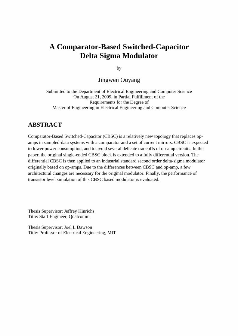
Comparator-Based Switched-Capacitor (CBSC) is a relatively new topology that replaces op-amps in sampled-data systems with a comparator and a set of current mirrors. CBSC is expected to lower power consumption, and to avoid several delicate tradeoffs of op-amp circuits. In this paper, the original single-ended CBSC block is extended to a fully differential version. The differential CBSC is then applied to an industrial standard second order delta-sigma modulator originally based on op-amps. Due to the differences between CBSC and op-amp, a few architectural changes are necessary for the original modulator. Finally, the performance of transistor level simulation of this CBSC based modulator is evaluated.
Thesis Supervisor: Jeffrey Hinrichs Title: Staff Engineer, Qualcomm
Thesis Supervisor: Joel L Dawson Title: Professor of Electrical Engineering, MIT
1
Contents
Chapter 1 Introduction ..................................................................................................... 7
1.1 Motivation ............................................................................................................. 7
1.2 Thesis Organization ............................................................................................... 8
Chapter 2 Intro to CBSC ................................................................................................ 10
2.1 CBSC Circuits vs Op-Amp Based Circuits ......................................................... 10
2.2 CBSC Charge Transfer Phase ............................................................................. 12
2.3 CBSC Application in Pipelined ADC ................................................................. 14
Chapter 3 An Op-Amp Based ΔΣ Ideal Circuit Design ................................................. 17
3.1 Operation and Architecture ................................................................................. 17
3.2 Circuit Implementation ....................................................................................... 20
Chapter 4 CBSC 2nd Order ΔΣ Modulator ..................................................................... 23
4.1 Differential CBSC without Preset Phase ............................................................. 23
4.2 CBSC Feed-Forward Path ................................................................................... 27
4.3 Delay ............................................................................................................. 31
2
4.4 Capacitor Sizing .................................................................................................. 32
4.5 Sampling Switches .............................................................................................. 33
4.6 CBSC Logic Block .............................................................................................. 36
4.7 Comparator .......................................................................................................... 39
4.8 Current Source ..................................................................................................... 42
4.9 Prototype CBSC 2nd Order ΔΣ Modulator ........................................................... 48
Chapter 5 Simulation Result .......................................................................................... 50
5.1 SNR ..................................................................................................................... 50
5.2 Power Usage ........................................................................................................ 53
Chapter 6 Conclusion ..................................................................................................... 54
Chapter 7 Future Work and Ideas .................................................................................. 55
Appendix A Calculations............................................................................................... 56
Appendix B Schematics ................................................................................................ 68
3
List of Figures
Figure 2–1: Op-amp based switched-capacitor gain stage transfer phase. (a)
Switched-capacitor circuit. (b) The output voltage exponentially settles
to the final values. (c) The summing node voltage exponentially settles
to the virtual ground condition.[4] .............................................................. 11
Figure 2–2: Comparator-based switched-capacitor gain stage charge transfer phase.
(a) Switched-capacitor circuit with an idealized zero delay comparator.
(b) The output voltage ramps to the final value. (c) The summing node
voltage ramps to the virtual ground condition. [4] ...................................... 11
Figure 2–3: Preset phase (P). (a) Switch P Closes. (b) grounded and brought
below [4] ............................................................................................. 13
Figure 2–4: Coarse charge transfer phase ( 1). (a) Current sourse 1 charges output.
(b) and ramp and overshoot their ideal values.[4] ............................ 13
Figure 2–5: Fine charge transfer phase ( 2). (a) Current source 2 discharges output.
(b) and ramp to their final values. [4] ................................................ 14
Figure 2–6: CBSC pipelined ADC design [4] .................................................................. 15
Figure 2–7: Sampling phase of pipelined ADC ................................................................ 15
Figure 3–1: Noise shaping curves and noise spectrum in ΔΣ modulator .......................... 18
Figure 3–2: Block diagram of a 2nd-order feed-forward ΔΣ modulator ............................ 19
4
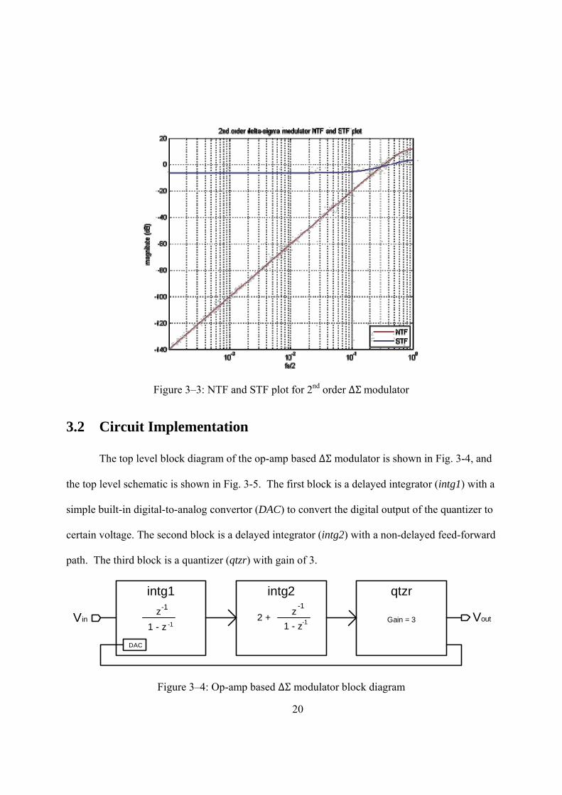
Figure 3–3: NTF and STF plot for 2nd order ΔΣ modulator .............................................. 20
Figure 3–4: Op-amp based ΔΣ modulator block diagram ................................................. 20
Figure 3–5: Top level Schematics of an op-amp based 2nd order ΔΣ modulator .............. 21
Figure 3–6: non-overlapping clock, phase-1 (P1) and phase-2 (P2) ................................ 22
Figure 4–1: Single ended to differential conversion ......................................................... 24
Figure 4–2: Pseudo differential design [7] ........................................................................ 24
Figure 4–3: Additional set of current course branch helps to make the CBSC operate
without constrain on the input range ........................................................... 26
Figure 4–4: Differential CBSC Block Diagram................................................................ 26
Figure 4–5: Current conflict between two CBSC driving stages ...................................... 28
Figure 4–6: CBSC ΔΣ modulator block diagram .............................................................. 29
Figure 4–7: Latched comparator used in quantizer ........................................................... 30
Figure 4–8: Sampling capacitor setups for quantizer ....................................................... 30
Figure 4–9: Single ended version of intg1 with dummy branch ....................................... 31
Figure 4–10: Demonstration of transmission gate on-resistance ..................................... 33
Figure 4–11: a sample RC circuit with step input current. ............................................... 34
Figure 4–12: a) Ideal behavior of comparator input voltage. b) Two types of effect
caused by on-resistance of the switch. c) Resulting behavior after error
correction. .................................................................................................... 35
Figure 4–13: State machine diagram for logic block ........................................................ 36
Figure 4–14: Example of the use of SR-FF. a) Set up. b) Resulting signal. ..................... 38
Figure 4–15: comparator design for CBSC block ............................................................. 39
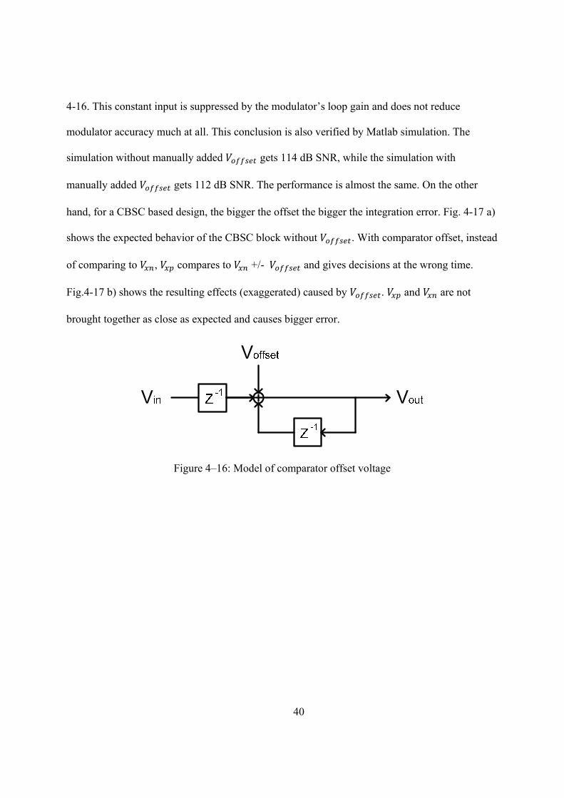
Figure 4–16: Model of comparator offset voltage ............................................................ 40
5
Figure 4–17: Error caused by comparator offset. A) Expected behavior. B) Error
cases ............................................................................................................ 41
Figure 4–19: Comparator offset distribution .................................................................... 42
Figure 4–19: Initial design of current mirror. A) E1 high, current source is on. B) E1
low, current source is off. ............................................................................ 43
Figure 4–20: Comparison between the ideal current source and actual current source
output currents ............................................................................................. 44
Figure 4–21: basic structure of charge-pump style current source ................................... 44
Figure 4–22: Equivalent circuit of charge-pump style current source when all the
branches are off. is on the order of mega ohms ................................ 45
Figure 4–23: Switch signals needs to match so that they reach about the
same time ..................................................................................................... 46
Figure 4–24: Switches are sized in a way that Is2 = Is3 << Is1 to reduce the turn-off
glitch at the output ....................................................................................... 46
Figure 4–25: Simplified schematic of current source in CBSC block .............................. 47
Figure 4–26: Top level schematics of a CBSC 2nd order ΔΣ modulator ........................... 49
Figure 5–1: Spectrum comparison of different versions of ΔΣ modulator ....................... 52
6
List of Tables
Table 1–1: Comparison of the four types of ADCs ............................................................ 8
Table 3–1: Coefficient values ........................................................................................... 19
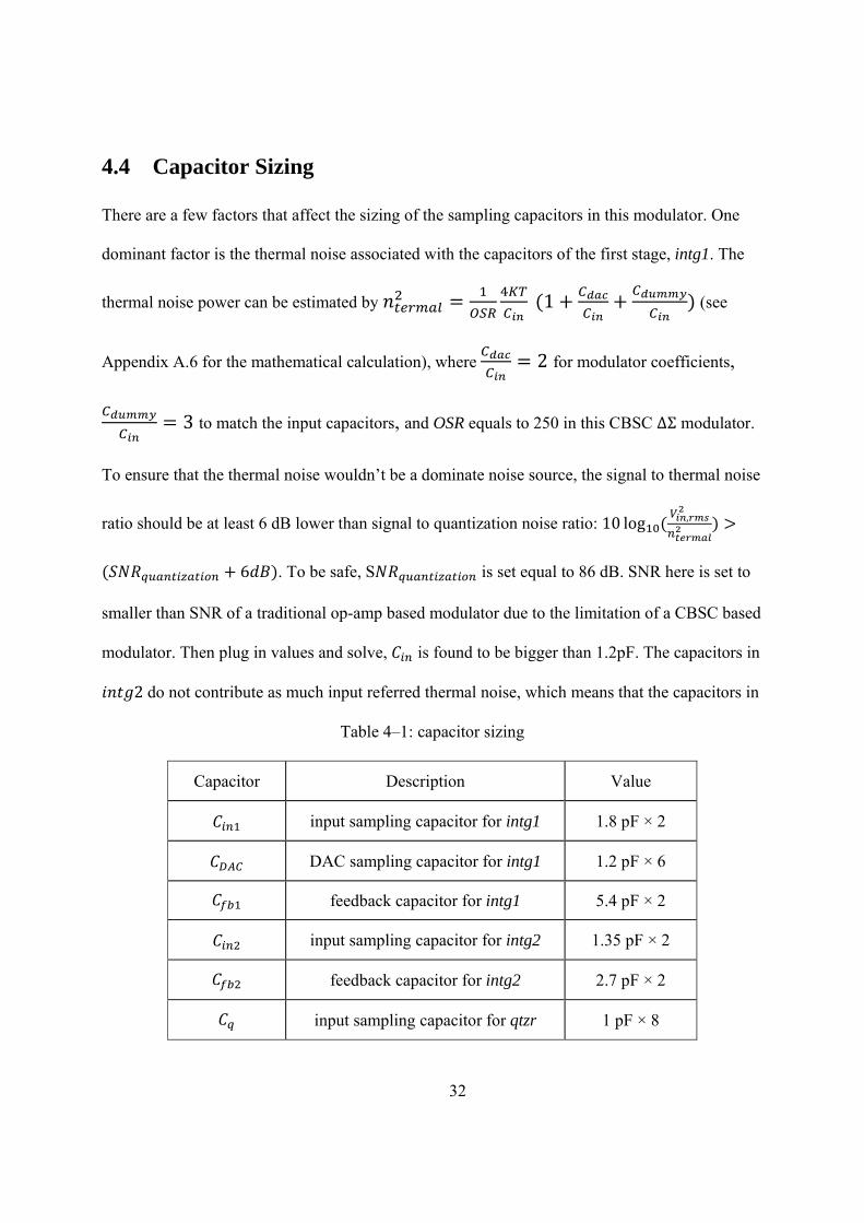
Table 4–1: capacitor sizing ............................................................................................... 32
Table 4–2: Set-reset flip flop operation table [8] .............................................................. 37
Table 5–1: Simulation setups ............................................................................................ 51
Table 5–2: resulting SNR from different versions ............................................................ 52
Table 5–3: Current usage comparison between the op-amp based and the CBSC
based ΔΣ modulator ..................................................................................... 53
7
Chapter 1
Introduction
1.1 Motivation
Advancement in modern technology has led to an increasing number of digital applications.
However, because we live in an analog world, we need to convert the analog signals into digital
signals before we can process them. The building block that is being used to accomplish this task
is called an Analog-to-Digital Converter (ADC). There are a few major ways to build an ADC.
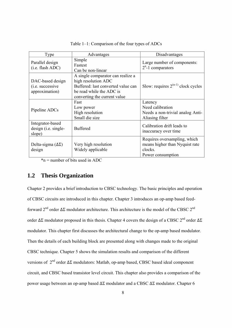
Each of them has its pros and cons [1] [2] [3]. As can be seen in Table 1-1, ΔΣ ADCs have the
advantage of offering the highest resolution of the various types.
However, ΔΣ ADCs have several drawbacks as well. It has becoming more and more
challenging to compensate op-amps for high gain-bandwidth in scaled technologies[4]. These
ADCs also suffer an increase in power consumption (mainly from op-amp usage) in order to
maintain conversion speed while the power supply is lowered [4]. In another words, op-amp has
become the bottleneck of ΔΣ ADCs in terms of meeting the power consumption and speed
requirements. As a potential solution to this problem, Comparator-based switched-capacitor
(CBSC) circuits are introduced in [4] to eliminate the usage of op-amps. This thesis discusses the
design and performance of a 2nd order ΔΣ modulator using CBSC circuits.
8
Table 1–1: Comparison of the four types of ADCs
Type Advantages Disadvantages
Parallel design (i.e. flash ADC)
Simple Fastest Can be non-linear
Large number of components: 2n-1 comparators
DAC-based design (i.e. successive approximation)
A single comparator can realize a high resolution ADC Buffered: last converted value can be read while the ADC is converting the current value
Slow: requires 2(n-1) clock cycles
Pipeline ADCs
Fast Low power High resolution Small die size
Latency Need calibration Needs a non-trivial analog Anti-Aliasing filter
Integrator-based design (i.e. single-slope)
Buffered Calibration drift leads to inaccuracy over time
Delta-sigma (ΔΣ) design
Very high resolution Widely applicable
Requires oversampling, which means higher than Nyquist rate clocks. Power consumption
*n = number of bits used in ADC
1.2 Thesis Organization
Chapter 2 provides a brief introduction to CBSC technology. The basic principles and operation
of CBSC circuits are introduced in this chapter. Chapter 3 introduces an op-amp based feed-
forward 2nd order ΔΣ modulator architecture. This architecture is the model of the CBSC 2nd
order ΔΣ modulator proposed in this thesis. Chapter 4 covers the design of a CBSC 2nd order ΔΣ
modulator. This chapter first discusses the architectural change to the op-amp based modulator.
Then the details of each building block are presented along with changes made to the original
CBSC technique. Chapter 5 shows the simulation results and comparison of the different
versions of 2nd order ΔΣ modulators: Matlab, op-amp based, CBSC based ideal component
circuit, and CBSC based transistor level circuit. This chapter also provides a comparison of the
power usage between an op-amp based ΔΣ modulator and a CBSC ΔΣ modulator. Chapter 6

9
discusses the advantages and the disadvantages of the CBSC ΔΣ modulator. In the end, future
work and ideas are suggested in Chapter 7.
10
Chapter 2
Intro to CBSC
2.1 CBSC Circuits vs Op-Amp Based Circuits
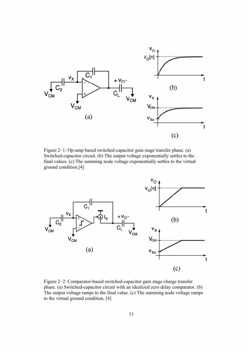
Fig. 2-1 and Fig. 2-2 from [4] both use the switched-capacitor architecture; however, in Fig. 2-2
the op-amp in Fig. 2-1 is replaced by a comparator. The main difference between the two
building blocks is that the op-amp forces the virtual ground while the comparator detects the
virtual ground. The output voltage plots show that they both have similar behavior, except that
one settles exponentially while the other one settles linearly. It can also be mathematically
proven that the comparator-based circuit works the same as the op-amp based circuit (see
Appendix A.1 and A.2).
There are several advantages of the comparator-based switched-capacitor (CBSC)
topology. First, just like the op-amp based switched capacitor circuits, the CBSC circuits use
two-phase clocking, sampling phase and evaluation phase. The difference is that in a CBSC
circuit all the current sources connected to the output nodes are off at the end of the evaluation
phase, which is good for low-voltage applications [5]. Second, preliminary analyses indicate that
detecting the virtual ground condition (CBSC circuits) is more energy efficient than forcing the
virtual ground (op-amp based circuits)[6]. Also, the op-amp approach has a feedback path, which
11
Figure 2–1: Op-amp based switched-capacitor gain stage transfer phase. (a) Switched-capacitor circuit. (b) The output voltage exponentially settles to the final values. (c) The summing node voltage exponentially settles to the virtual ground condition.[4]
Figure 2–2: Comparator-based switched-capacitor gain stage charge transfer phase. (a) Switched-capacitor circuit with an idealized zero delay comparator. (b) The output voltage ramps to the final value. (c) The summing node voltage ramps to the virtual ground condition. [4]
12
needs to be stabilized. The techniques used to stabilize the amplifier require increased power
consumption to maintain the same operational speed [4]. On the other hand, CBSC does not have
a stability problem because it has an open-loop. Thus, CBSC doesn’t consume as much power.
Finally, the CBSC design methodology is expected to be applicable to a wide range of
capacitively loaded switched-capacitor circuits and expected to be compatible with most known
architectures [4]. However, successful implementation of CBSC ΔΣ modulator with real test
results is not demonstrated in literature yet.
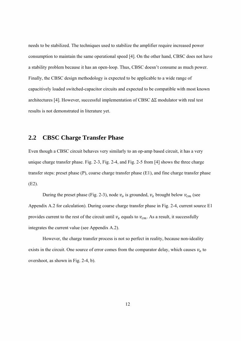
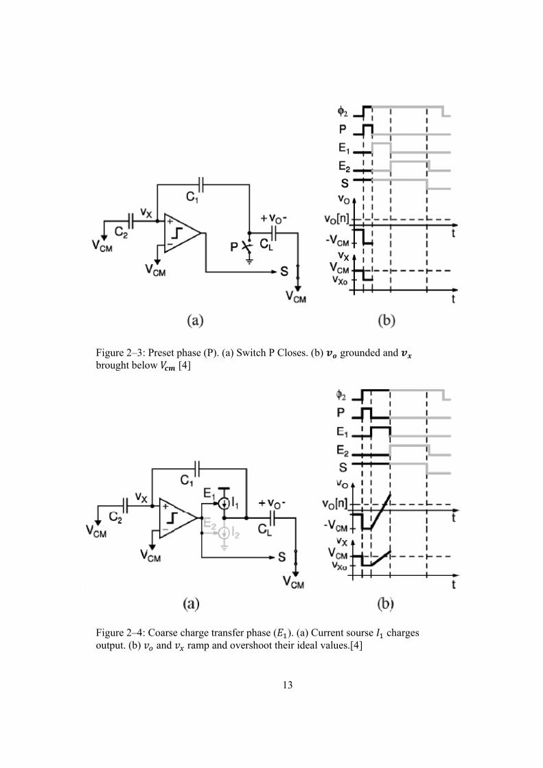
2.2 CBSC Charge Transfer Phase
Even though a CBSC circuit behaves very similarly to an op-amp based circuit, it has a very
unique charge transfer phase. Fig. 2-3, Fig. 2-4, and Fig. 2-5 from [4] shows the three charge
transfer steps: preset phase (P), coarse charge transfer phase (E1), and fine charge transfer phase
(E2).
During the preset phase (Fig. 2-3), node is grounded, brought below (see
Appendix A.2 for calculation). During coarse charge transfer phase in Fig. 2-4, current source E1
provides current to the rest of the circuit until equals to . As a result, it successfully
integrates the current value (see Appendix A.2).
However, the charge transfer process is not so perfect in reality, because non-ideality
exists in the circuit. One source of error comes from the comparator delay, which causes to
overshoot, as shown in Fig. 2-4, b).
13
Figure 2–3: Preset phase (P). (a) Switch P Closes. (b) grounded and brought below [4]
Figure 2–4: Coarse charge transfer phase ( ). (a) Current sourse charges output. (b) and ramp and overshoot their ideal values.[4]
14
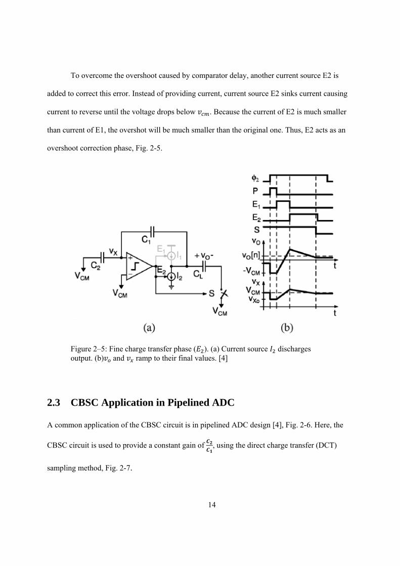
To overcome the overshoot caused by comparator delay, another current source E2 is
added to correct this error. Instead of providing current, current source E2 sinks current causing
current to reverse until the voltage drops below . Because the current of E2 is much smaller
than current of E1, the overshot will be much smaller than the original one. Thus, E2 acts as an
overshoot correction phase, Fig. 2-5.
Figure 2–5: Fine charge transfer phase ( ). (a) Current source discharges output. (b) and ramp to their final values. [4]
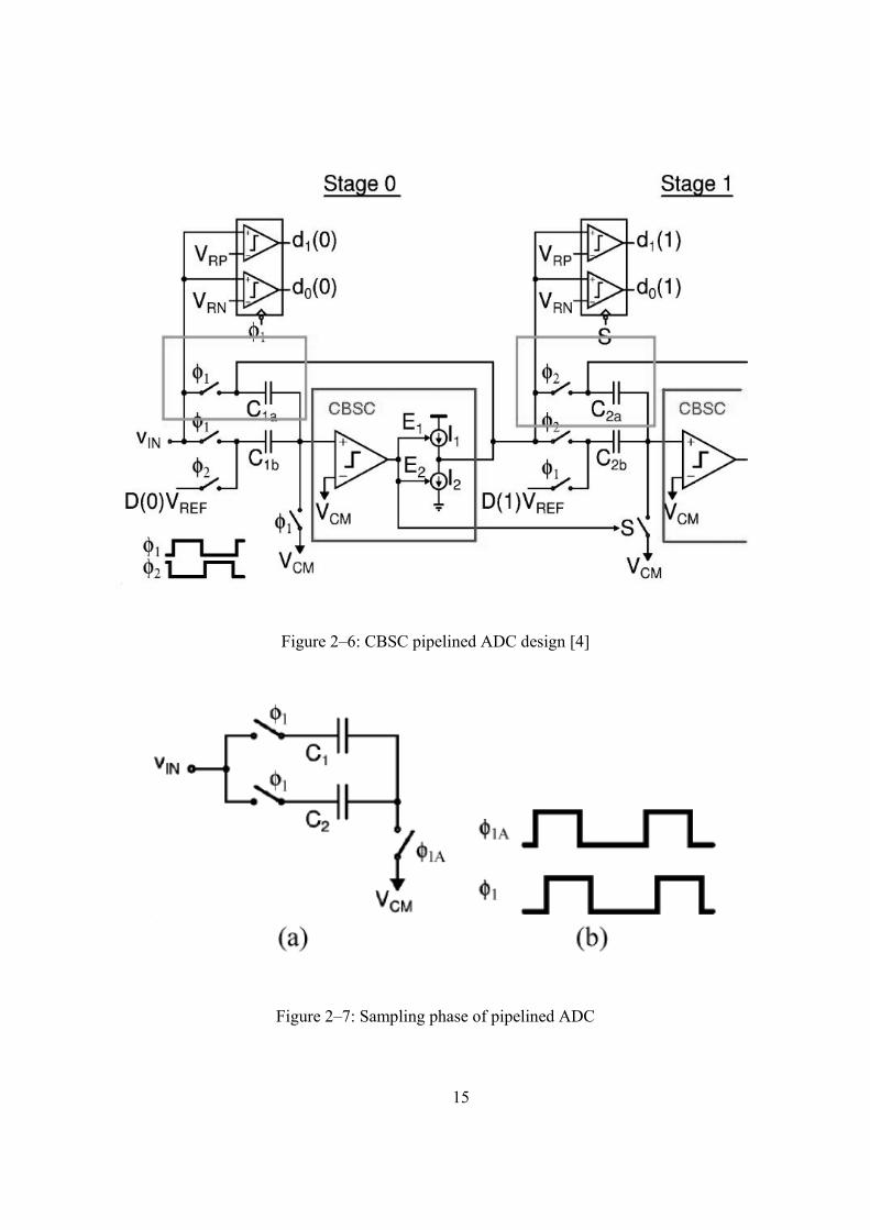
2.3 CBSC Application in Pipelined ADC
A common application of the CBSC circuit is in pipelined ADC design [4], Fig. 2-6. Here, the
CBSC circuit is used to provide a constant gain of , using the direct charge transfer (DCT)
sampling method, Fig. 2-7.
15
Figure 2–6: CBSC pipelined ADC design [4]
Figure 2–7: Sampling phase of pipelined ADC
16
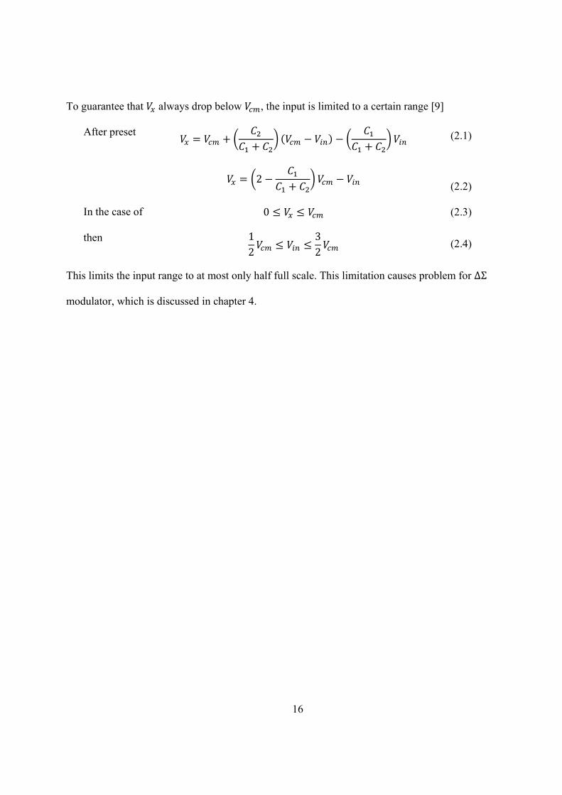
To guarantee that always drop below , the input is limited to a certain range [9]
After preset
2
(2.1)
(2.2)
In the case of 0 (2.3)
then 12
32 (2.4)
This limits the input range to at most only half full scale. This limitation causes problem for ΔΣ
modulator, which is discussed in chapter 4.
17
Chapter 3
An Op-Amp Based Ideal Circuit Design
The basic theory of the comparator-based switched-circuit (CBSC) is explained in Chapter 2.
The next step is to apply this theory to a practical design of a 2nd-order ΔΣ modulator. This
chapter provides a brief overview of a particular op-amp based ΔΣ modulator structure that is
being converted to a CBSC version.
3.1 Operation and Architecture
ΔΣ modulation is based on the technique of oversampling to reduce the noise in the band of
interest (left shaded area of Fig. 3-1 [7]), which also avoids using high-precision analog circuits
for the anti-aliasing filter [7]. Another important property of ΔΣ modulator is noise shaping. For
a first order ΔΣ modulator, noise is being shaped by the function 1 ; for a nth
order ΔΣ modulator, noise is being shaped by the function 1 , resulting in in-band
quantization noise variance to equal to [7], where OSR represents the
oversampling rate. On the system level, there are many ways to realize a ΔΣ modulator. Richard
Schreier has provided a very convenient MATLAB tool box “delsig” (available at
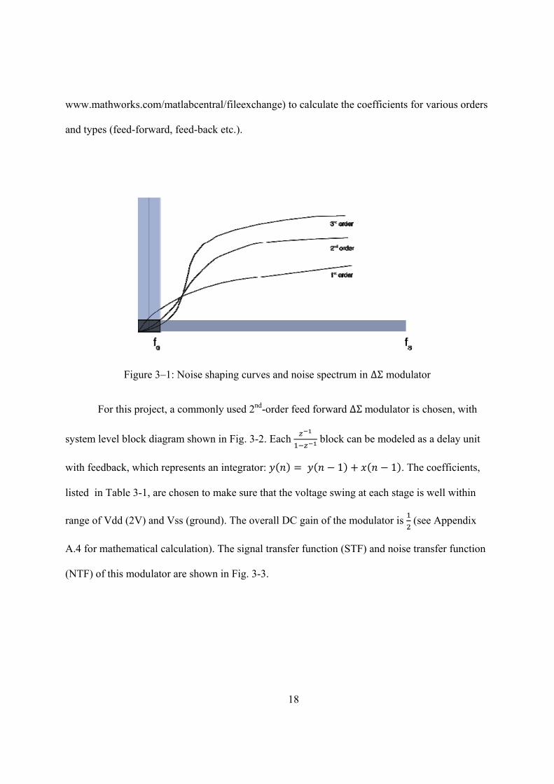
18
www.mathworks.com/matlabcentral/fileexchange) to calculate the coefficients for various orders
and types (feed-forward, feed-back etc.).
Figure 3–1: Noise shaping curves and noise spectrum in ΔΣ modulator
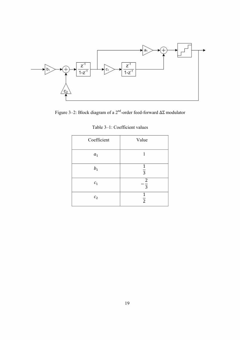
For this project, a commonly used 2nd-order feed forward ΔΣ modulator is chosen, with
system level block diagram shown in Fig. 3-2. Each block can be modeled as a delay unit
with feedback, which represents an integrator: 1 1 . The coefficients,
listed in Table 3-1, are chosen to make sure that the voltage swing at each stage is well within
range of Vdd (2V) and Vss (ground). The overall DC gain of the modulator is (see Appendix
A.4 for mathematical calculation). The signal transfer function (STF) and noise transfer function
(NTF) of this modulator are shown in Fig. 3-3.
19
Figure 3–2: Block diagram of a 2nd-order feed-forward ΔΣ modulator
Table 3–1: Coefficient values
Coefficient Value
1
13
23
12
20
Figure 3–3: NTF and STF plot for 2nd order ΔΣ modulator
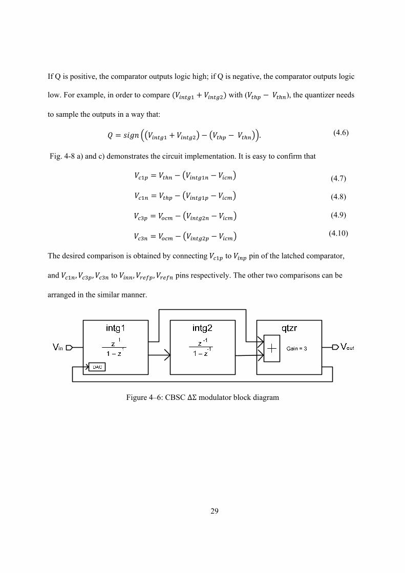
3.2 Circuit Implementation
The top level block diagram of the op-amp based ΔΣ modulator is shown in Fig. 3-4, and
the top level schematic is shown in Fig. 3-5. The first block is a delayed integrator (intg1) with a
simple built-in digital-to-analog convertor (DAC) to convert the digital output of the quantizer to
certain voltage. The second block is a delayed integrator (intg2) with a non-delayed feed-forward
path. The third block is a quantizer (qtzr) with gain of 3.
intg1 intg2 qtzr
DAC
Vin Vout1 - z
-1
-1z
1 - z
-1
-1
zGain = 32 +
Figure 3–4: Op-amp based ΔΣ modulator block diagram
21
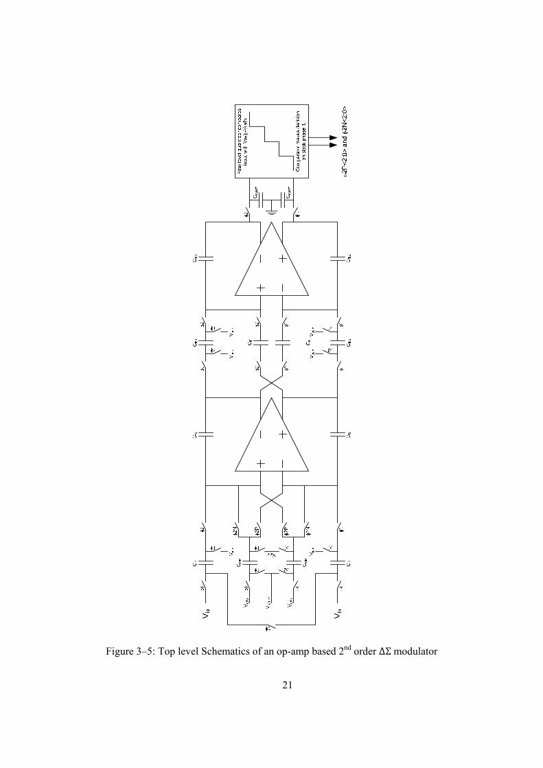
Figure 3–5: Top level Schematics of an op-amp based 2nd order ΔΣ modulator
22
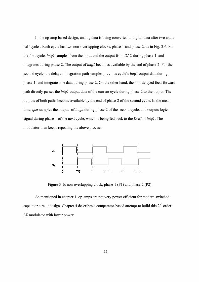
In the op-amp based design, analog data is being converted to digital data after two and a
half cycles. Each cycle has two non-overlapping clocks, phase-1 and phase-2, as in Fig. 3-6. For
the first cycle, intg1 samples from the input and the output from DAC during phase-1, and
integrates during phase-2. The output of intg1 becomes available by the end of phase-2. For the
second cycle, the delayed integration path samples previous cycle’s intg1 output data during
phase-1, and integrates the data during phase-2. On the other hand, the non-delayed feed-forward
path directly passes the intg1 output data of the current cycle during phase-2 to the output. The
outputs of both paths become available by the end of phase-2 of the second cycle. In the mean
time, qtzr samples the outputs of intg2 during phase-2 of the second cycle, and outputs logic
signal during phase-1 of the next cycle, which is being fed back to the DAC of intg1. The
modulator then keeps repeating the above process.
Figure 3–6: non-overlapping clock, phase-1 (P1) and phase-2 (P2)
As mentioned in chapter 1, op-amps are not very power efficient for modern switched-
capacitor circuit design. Chapter 4 describes a comparator-based attempt to build this 2nd order
ΔΣ modulator with lower power.
23
Chapter 4
CBSC 2nd Order Modulator
Mathematically, the CBSC block works pretty much the same as an op-amp; however, there are
many differences when it comes to circuit design. This chapter describes some changes made to
the basic 2nd order ΔΣ Modulator structure, and the implementation of a CBSC version.
4.1 Differential CBSC without Preset Phase
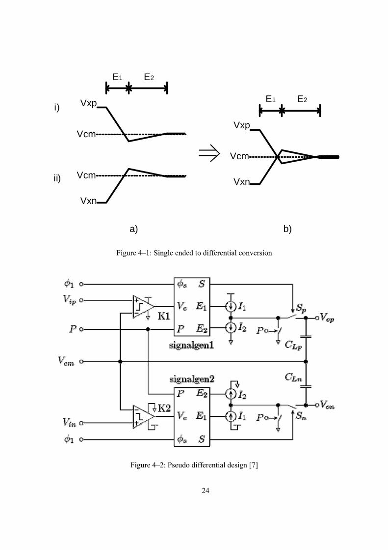
In order to get better performance, a differential version is designed based on the original
single-ended CBSC circuit. It is very easy to get a pseudo differential version. Imagine that there
are two inputs at the input of two identical single-ended CBSC integrators: the input at is
initially larger than input common mode voltage ( ), and the input at is smaller than .
The resulting and voltages are shown in Fig. 4-1 a). Put the two single-ended CBSC
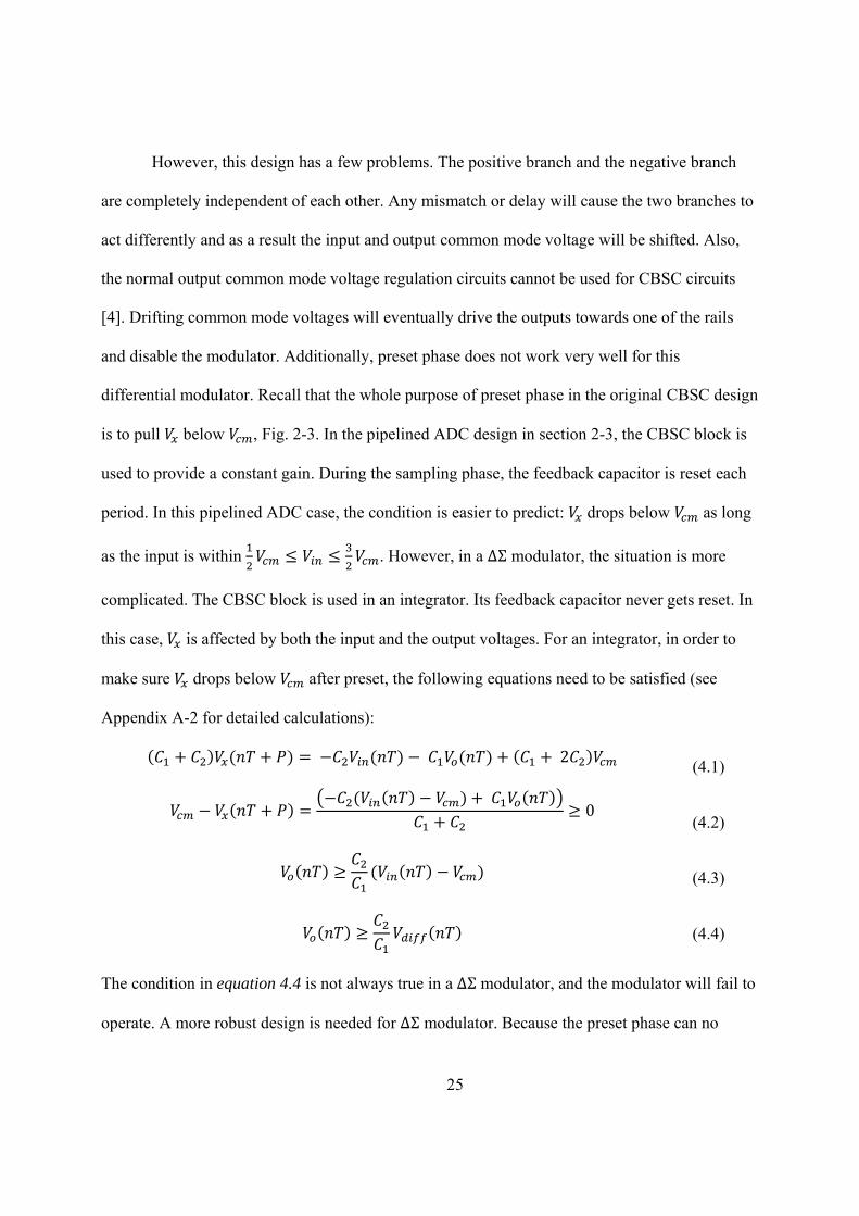
blocks together, Fig. 4-1 b), we get a pseudo differential version, Fig. 4-2 [10].
24
b)
E1 E2
Vxp
Vxn
E1 E2
Vxp
Vxn
Vcm
Vcm
Vcm
a)
i)
ii)
Figure 4–1: Single ended to differential conversion
Figure 4–2: Pseudo differential design [7]
25
However, this design has a few problems. The positive branch and the negative branch
are completely independent of each other. Any mismatch or delay will cause the two branches to
act differently and as a result the input and output common mode voltage will be shifted. Also,
the normal output common mode voltage regulation circuits cannot be used for CBSC circuits
[4]. Drifting common mode voltages will eventually drive the outputs towards one of the rails
and disable the modulator. Additionally, preset phase does not work very well for this
differential modulator. Recall that the whole purpose of preset phase in the original CBSC design
is to pull below , Fig. 2-3. In the pipelined ADC design in section 2-3, the CBSC block is
used to provide a constant gain. During the sampling phase, the feedback capacitor is reset each
period. In this pipelined ADC case, the condition is easier to predict: drops below as long
as the input is within . However, in a ΔΣ modulator, the situation is more
complicated. The CBSC block is used in an integrator. Its feedback capacitor never gets reset. In
this case, is affected by both the input and the output voltages. For an integrator, in order to
make sure drops below after preset, the following equations need to be satisfied (see
Appendix A-2 for detailed calculations):
2
0
(4.1)
(4.2)
(4.3)
(4.4)
The condition in equation 4.4 is not always true in a ΔΣ modulator, and the modulator will fail to
operate. A more robust design is needed for ΔΣ modulator. Because the preset phase can no
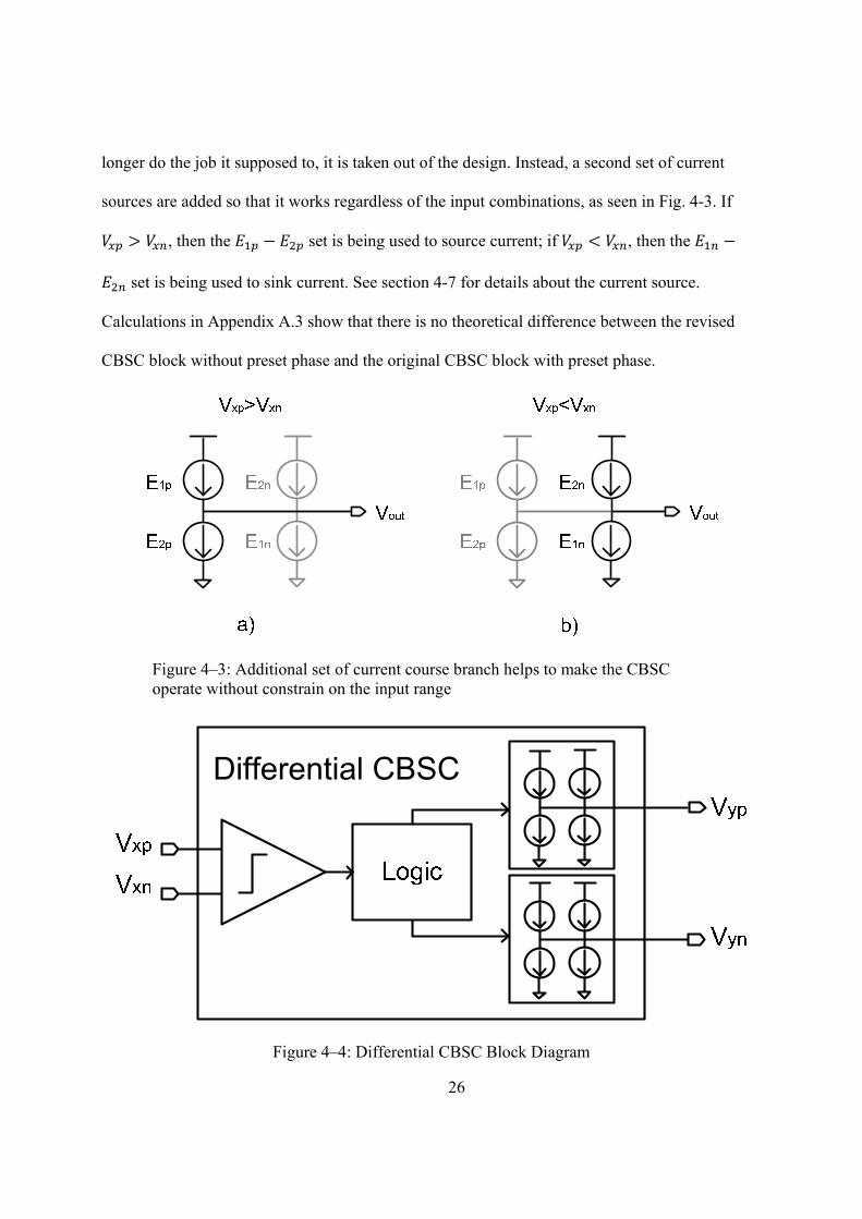
26
longer do the job it supposed to, it is taken out of the design. Instead, a second set of current
sources are added so that it works regardless of the input combinations, as seen in Fig. 4-3. If
, then the set is being used to source current; if , then the
set is being used to sink current. See section 4-7 for details about the current source.
Calculations in Appendix A.3 show that there is no theoretical difference between the revised
CBSC block without preset phase and the original CBSC block with preset phase.
Figure 4–3: Additional set of current course branch helps to make the CBSC operate without constrain on the input range
Figure 4–4: Differential CBSC Block Diagram
27
4.2 CBSC Feed-Forward Path Issue
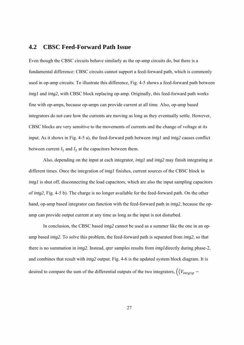
Even though the CBSC circuits behave similarly as the op-amp circuits do, but there is a
fundamental difference: CBSC circuits cannot support a feed-forward path, which is commonly
used in op-amp circuits. To illustrate this difference, Fig. 4-5 shows a feed-forward path between
intg1 and intg2, with CBSC block replacing op-amp. Originally, this feed-forward path works
fine with op-amps, because op-amps can provide current at all time. Also, op-amp based
integrators do not care how the currents are moving as long as they eventually settle. However,
CBSC blocks are very sensitive to the movements of currents and the change of voltage at its
input. As it shows in Fig. 4-5 a), the feed-forward path between intg1 and intg2 causes conflict
between current and at the capacitors between them.
Also, depending on the input at each integrator, intg1 and intg2 may finish integrating at
different times. Once the integration of intg1 finishes, current sources of the CBSC block in
intg1 is shut off, disconnecting the load capacitors, which are also the input sampling capacitors
of intg2, Fig. 4-5 b). The charge is no longer available for the feed-forward path. On the other
hand, op-amp based integrator can function with the feed-forward path in intg2, because the op-
amp can provide output current at any time as long as the input is not disturbed.
In conclusion, the CBSC based intg2 cannot be used as a summer like the one in an op-
amp based intg2. To solve this problem, the feed-forward path is separated from intg2, so that
there is no summation in intg2. Instead, qtzr samples results from intg1directly during phase-2,
and combines that result with intg2 output. Fig. 4-6 is the updated system block diagram. It is
desired to compare the sum of the differential outputs of the two integrators,
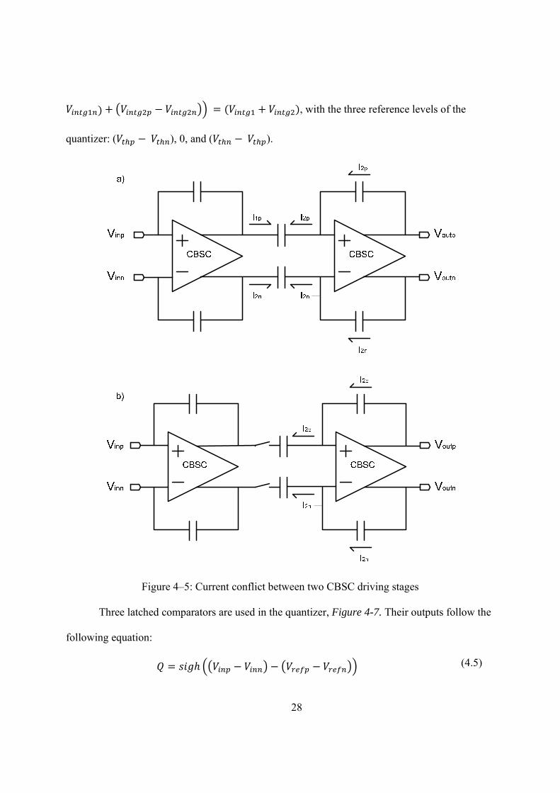
28
, with the three reference levels of the
quantizer: ( ), 0, and ( ).
Figure 4–5: Current conflict between two CBSC driving stages
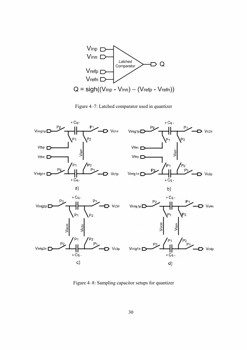
Three latched comparators are used in the quantizer, Figure 4-7. Their outputs follow the
following equation:
(4.5)
29
If Q is positive, the comparator outputs logic high; if Q is negative, the comparator outputs logic
low. For example, in order to compare with ( ), the quantizer needs
to sample the outputs in a way that:
. (4.6)
Fig. 4-8 a) and c) demonstrates the circuit implementation. It is easy to confirm that
(4.7)
(4.8)
(4.9)
(4.10)
The desired comparison is obtained by connecting to pin of the latched comparator,
and , , to , , pins respectively. The other two comparisons can be
arranged in the similar manner.
Figure 4–6: CBSC ΔΣ modulator block diagram
30
Figure 4–7: Latched comparator used in quantizer
Figure 4–8: Sampling capacitor setups for quantizer
31
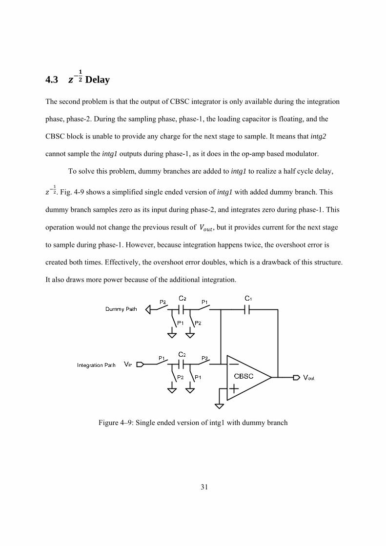
4.3 Delay
The second problem is that the output of CBSC integrator is only available during the integration
phase, phase-2. During the sampling phase, phase-1, the loading capacitor is floating, and the
CBSC block is unable to provide any charge for the next stage to sample. It means that intg2
cannot sample the intg1 outputs during phase-1, as it does in the op-amp based modulator.
To solve this problem, dummy branches are added to intg1 to realize a half cycle delay,
. Fig. 4-9 shows a simplified single ended version of intg1 with added dummy branch. This
dummy branch samples zero as its input during phase-2, and integrates zero during phase-1. This
operation would not change the previous result of , but it provides current for the next stage
to sample during phase-1. However, because integration happens twice, the overshoot error is
created both times. Effectively, the overshoot error doubles, which is a drawback of this structure.
It also draws more power because of the additional integration.
Figure 4–9: Single ended version of intg1 with dummy branch
32
4.4 Capacitor Sizing
There are a few factors that affect the sizing of the sampling capacitors in this modulator. One
dominant factor is the thermal noise associated with the capacitors of the first stage, intg1. The
thermal noise power can be estimated by 1 (see
Appendix A.6 for the mathematical calculation), where 2 for modulator coefficients,
3 to match the input capacitors, and OSR equals to 250 in this CBSC ΔΣ modulator.
To ensure that the thermal noise wouldn’t be a dominate noise source, the signal to thermal noise
ratio should be at least 6 dB lower than signal to quantization noise ratio: 10 log ,
6 . To be safe, S is set equal to 86 dB. SNR here is set to
smaller than SNR of a traditional op-amp based modulator due to the limitation of a CBSC based
modulator. Then plug in values and solve, is found to be bigger than 1.2pF. The capacitors in
2 do not contribute as much input referred thermal noise, which means that the capacitors in
Table 4–1: capacitor sizing
Capacitor Description Value
input sampling capacitor for intg1 1.8 pF × 2
DAC sampling capacitor for intg1 1.2 pF × 6
feedback capacitor for intg1 5.4 pF × 2
input sampling capacitor for intg2 1.35 pF × 2
feedback capacitor for intg2 2.7 pF × 2
input sampling capacitor for qtzr 1 pF × 8
33
intg2 could be even smaller. However, because leakage currents have greater effect on smaller
capacitors than larger ones, the capacitors cannot be too small. Also, larger capacitors require
larger current. As a result, the capacitor sizes are set as shown in Table 4-1 for a better overall
performance of the modulator. The optimal values yet need to be found.
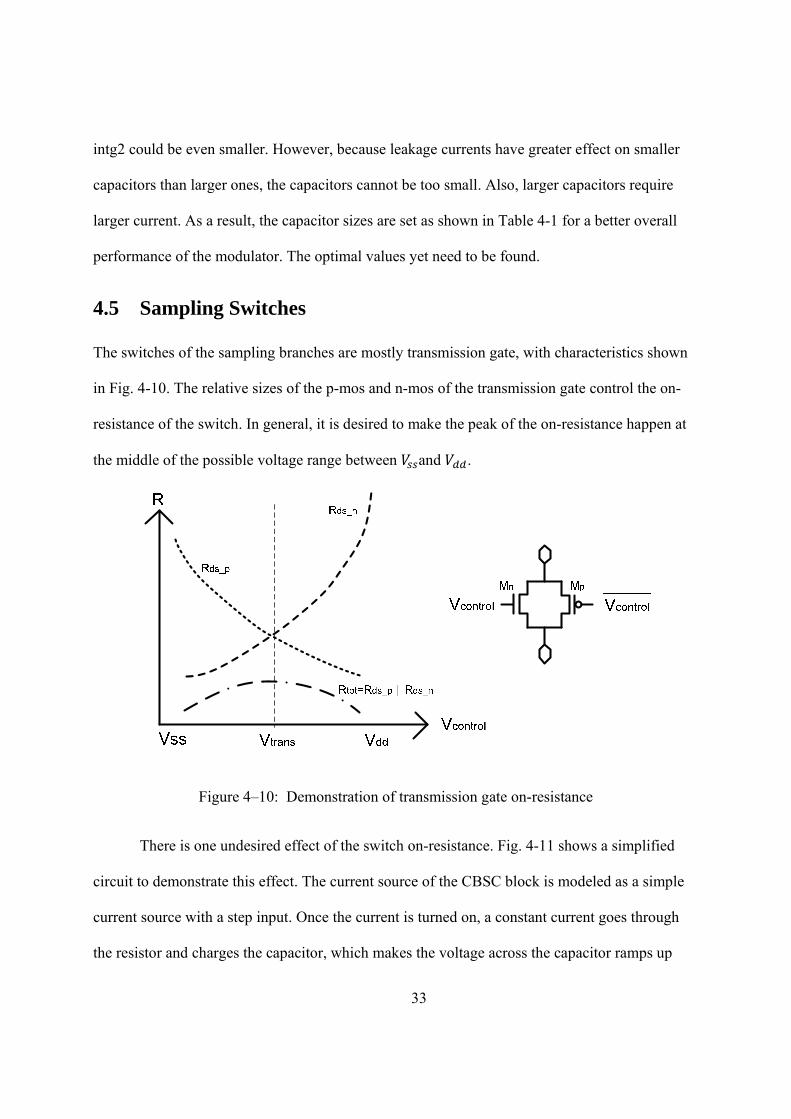
4.5 Sampling Switches
The switches of the sampling branches are mostly transmission gate, with characteristics shown
in Fig. 4-10. The relative sizes of the p-mos and n-mos of the transmission gate control the on-
resistance of the switch. In general, it is desired to make the peak of the on-resistance happen at
the middle of the possible voltage range between and .
Figure 4–10: Demonstration of transmission gate on-resistance
There is one undesired effect of the switch on-resistance. Fig. 4-11 shows a simplified
circuit to demonstrate this effect. The current source of the CBSC block is modeled as a simple
current source with a step input. Once the current is turned on, a constant current goes through
the resistor and charges the capacitor, which makes the voltage across the capacitor ramps up
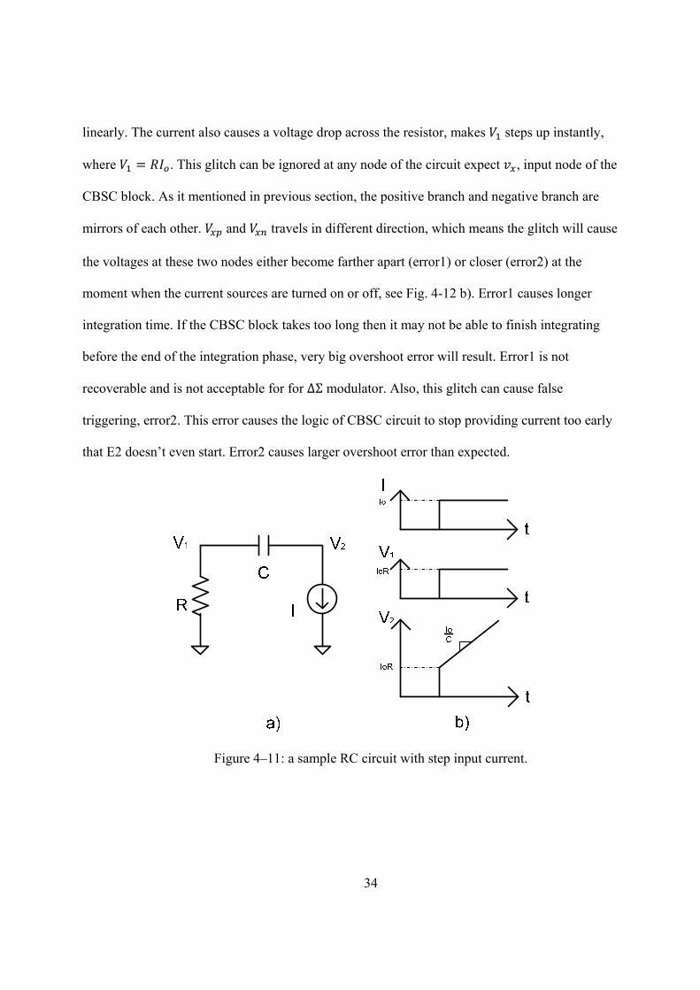
34
linearly. The current also causes a voltage drop across the resistor, makes steps up instantly,
where . This glitch can be ignored at any node of the circuit expect , input node of the
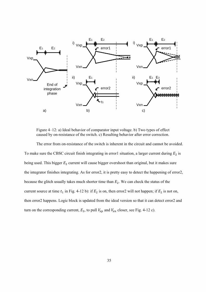
CBSC block. As it mentioned in previous section, the positive branch and negative branch are
mirrors of each other. and travels in different direction, which means the glitch will cause
the voltages at these two nodes either become farther apart (error1) or closer (error2) at the
moment when the current sources are turned on or off, see Fig. 4-12 b). Error1 causes longer
integration time. If the CBSC block takes too long then it may not be able to finish integrating
before the end of the integration phase, very big overshoot error will result. Error1 is not
recoverable and is not acceptable for for ΔΣ modulator. Also, this glitch can cause false
triggering, error2. This error causes the logic of CBSC circuit to stop providing current too early
that E2 doesn’t even start. Error2 causes larger overshoot error than expected.
Figure 4–11: a sample RC circuit with step input current.
35
i)
ii)
a) b)
E1 E2
E1 E2
E1
error1
error2
Vxp
Vxn
Vxp
Vxn
Vxp
Vxn
i)
ii)
c)
E1 E2
E1
error1
error2
Vxp
Vxn
Vxp
Vxn
E3
End of integration
phase
t1
Figure 4–12: a) Ideal behavior of comparator input voltage. b) Two types of effect caused by on-resistance of the switch. c) Resulting behavior after error correction.
The error from on-resistance of the switch is inherent in the circuit and cannot be avoided.
To make sure the CBSC circuit finish integrating in error1 situation, a larger current during is
being used. This bigger current will cause bigger overshoot than original, but it makes sure
the integrator finishes integrating. As for error2, it is pretty easy to detect the happening of error2,
because the glitch usually takes much shorter time than . We can check the status of the
current source at time in Fig. 4-12 b): if is on, then error2 will not happen; if is not on,
then error2 happens. Logic block is updated from the ideal version so that it can detect error2 and
turn on the corresponding current, , to pull and closer, see Fig. 4-12 c).
36
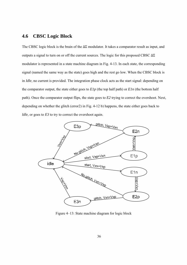
4.6 CBSC Logic Block
The CBSC logic block is the brain of the ΔΣ modulator. It takes a comparator result as input, and
outputs a signal to turn on or off the current sources. The logic for this proposed CBSC ΔΣ
modulator is represented in a state machine diagram in Fig. 4-13. In each state, the corresponding
signal (named the same way as the state) goes high and the rest go low. When the CBSC block is
in Idle, no current is provided. The integration phase clock acts as the start signal: depending on
the comparator output, the state either goes to E1p (the top half path) or E1n (the bottom half
path). Once the comparator output flips, the state goes to E2 trying to correct the overshoot. Next,
depending on whether the glitch (error2) in Fig. 4-12 b) happens, the state either goes back to
Idle, or goes to E3 to try to correct the overshoot again.
Figure 4–13: State machine diagram for logic block
37
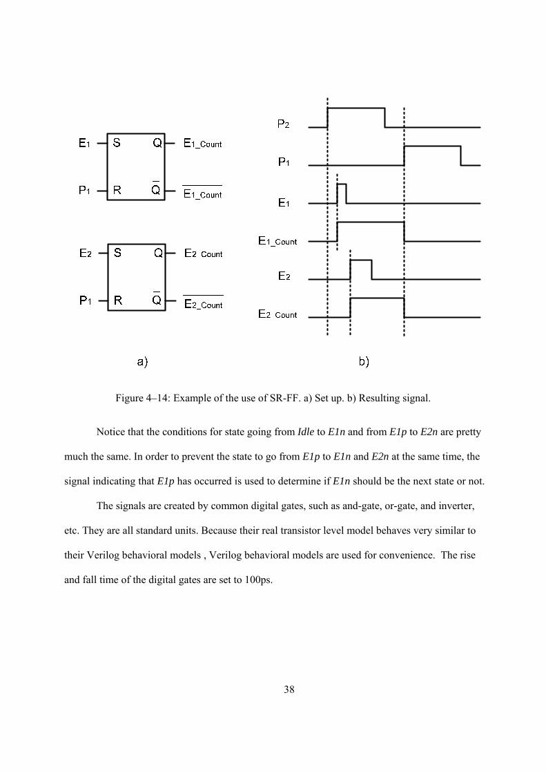
As shown in the state machine diagram, it's the change of the comparator output values
( or ) that triggers the change of states. In order to know which state is next, logic block
needs to know what the current state is. For this purpose, set-reset flip flops (SR-FF) are used as
counters. The operation of the SR-FF are summarized in Table 4-2 [8]. The reset (R) signal is the
sampling clock for each SR-FF, so that the states are reset in idle state. The set (S) signal is the
corresponding signal in each state. Once that signal goes high, the SR-FF is set and will not be
reset till the next phase. For example, in order to create _ and _ signals to indicate
that or have come up, the SR-FFs are connected as shown in Fig. 4-14 a), the outputs are
shown in Fig. 4-14 b). E _ and E _ are low in the beginning. During , remains low
the whole time. Once E goes high, SR-FF set _ to high. After drops low, E goes high,
SR-FF set _ to high. Then, _ and _ remains high until goes high to reset
them. These output signals created by the SR-FF are good indications of whether certain state
has occurred or not.
Table 4–2: Set-reset flip flop operation table [8]
SR Flip-Flop operationCharacteristic table Excitation table
S R Action Q(t) Q(t+1) S R Action 0 0 Keep state 0 0 0 X No change 0 1 Q = 0 0 1 1 0 Set 1 0 Q = 1 1 0 0 1 Reset
1 1 Unstable combination,race condition 1 1 X 0 No change
('X' denotes a do not care condition; meaning the signal is irrelevant)
38
Figure 4–14: Example of the use of SR-FF. a) Set up. b) Resulting signal.
Notice that the conditions for state going from Idle to E1n and from E1p to E2n are pretty
much the same. In order to prevent the state to go from E1p to E1n and E2n at the same time, the
signal indicating that E1p has occurred is used to determine if E1n should be the next state or not.
The signals are created by common digital gates, such as and-gate, or-gate, and inverter,
etc. They are all standard units. Because their real transistor level model behaves very similar to
their Verilog behavioral models , Verilog behavioral models are used for convenience. The rise
and fall time of the digital gates are set to 100ps.
39
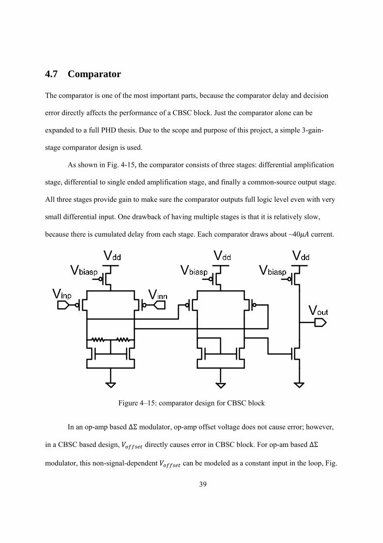
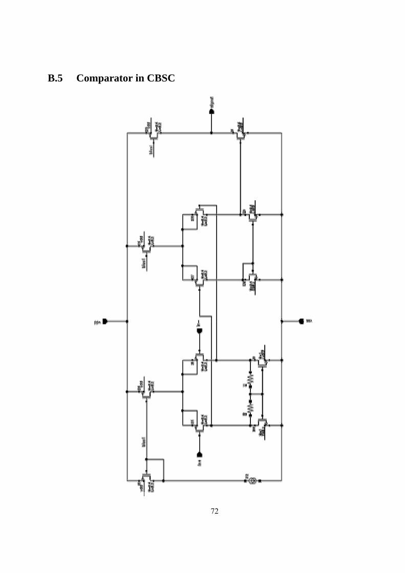
4.7 Comparator
The comparator is one of the most important parts, because the comparator delay and decision
error directly affects the performance of a CBSC block. Just the comparator alone can be
expanded to a full PHD thesis. Due to the scope and purpose of this project, a simple 3-gain-
stage comparator design is used.
As shown in Fig. 4-15, the comparator consists of three stages: differential amplification
stage, differential to single ended amplification stage, and finally a common-source output stage.
All three stages provide gain to make sure the comparator outputs full logic level even with very
small differential input. One drawback of having multiple stages is that it is relatively slow,
because there is cumulated delay from each stage. Each comparator draws about ~40 current.
Figure 4–15: comparator design for CBSC block
In an op-amp based ΔΣ modulator, op-amp offset voltage does not cause error; however,
in a CBSC based design, directly causes error in CBSC block. For op-am based ΔΣ
modulator, this non-signal-dependent can be modeled as a constant input in the loop, Fig.
40
4-16. This constant input is suppressed by the modulator’s loop gain and does not reduce
modulator accuracy much at all. This conclusion is also verified by Matlab simulation. The
simulation without manually added gets 114 dB SNR, while the simulation with
manually added gets 112 dB SNR. The performance is almost the same. On the other
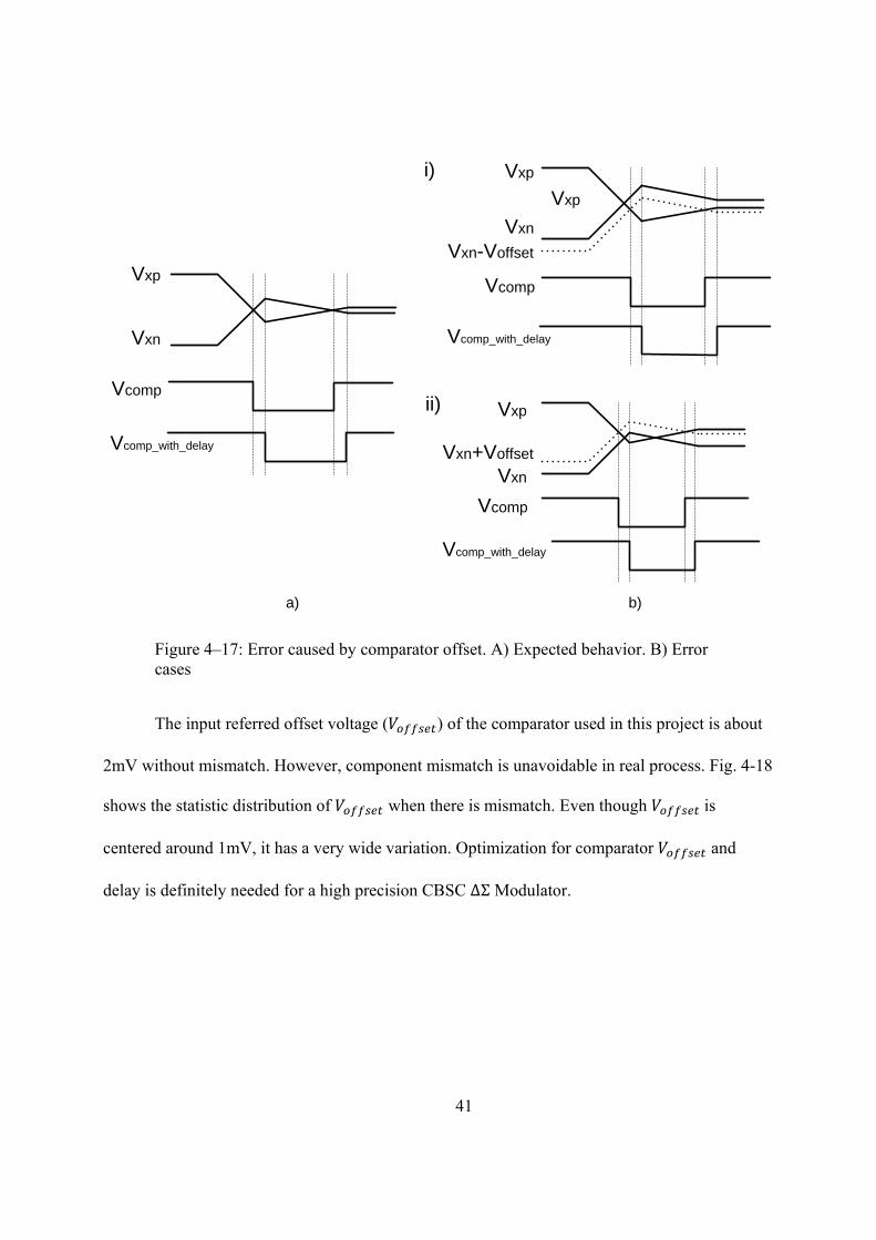
hand, for a CBSC based design, the bigger the offset the bigger the integration error. Fig. 4-17 a)
shows the expected behavior of the CBSC block without . With comparator offset, instead
of comparing to , compares to +/- and gives decisions at the wrong time.
Fig.4-17 b) shows the resulting effects (exaggerated) caused by . and are not
brought together as close as expected and causes bigger error.
Figure 4–16: Model of comparator offset voltage
41
Vxp
Vxp
Vxn
Vxp
VxnVxn-Voffset
Vxp
VxnVxn+Voffset
i)
ii)
a) b)
Vcomp
Vcomp
Vcomp
Vcomp_with_delay
Vcomp_with_delay
Vcomp_with_delay
Figure 4–17: Error caused by comparator offset. A) Expected behavior. B) Error cases
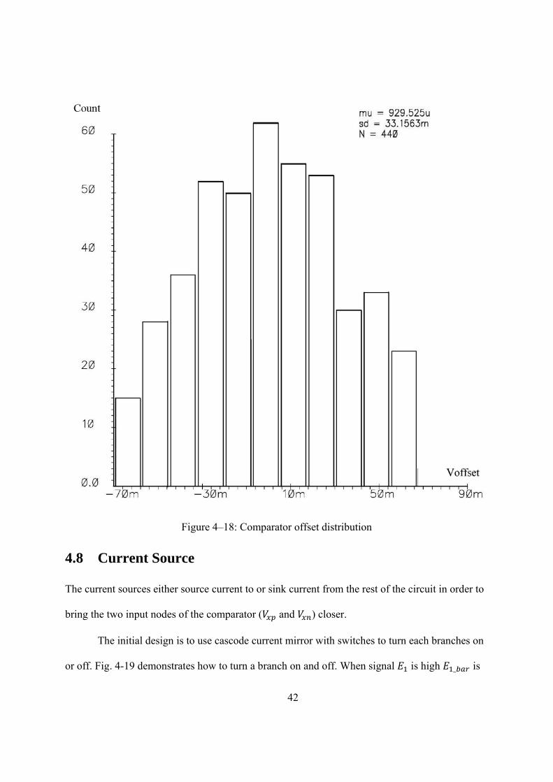
The input referred offset voltage ( ) of the comparator used in this project is about
2mV without mismatch. However, component mismatch is unavoidable in real process. Fig. 4-18
shows the statistic distribution of when there is mismatch. Even though is
centered around 1mV, it has a very wide variation. Optimization for comparator and
delay is definitely needed for a high precision CBSC ΔΣ Modulator.
42
Figure 4–18: Comparator offset distribution
4.8 Current Source
The current sources either source current to or sink current from the rest of the circuit in order to
bring the two input nodes of the comparator ( and ) closer.
The initial design is to use cascode current mirror with switches to turn each branches on
or off. Fig. 4-19 demonstrates how to turn a branch on and off. When signal is high _ is
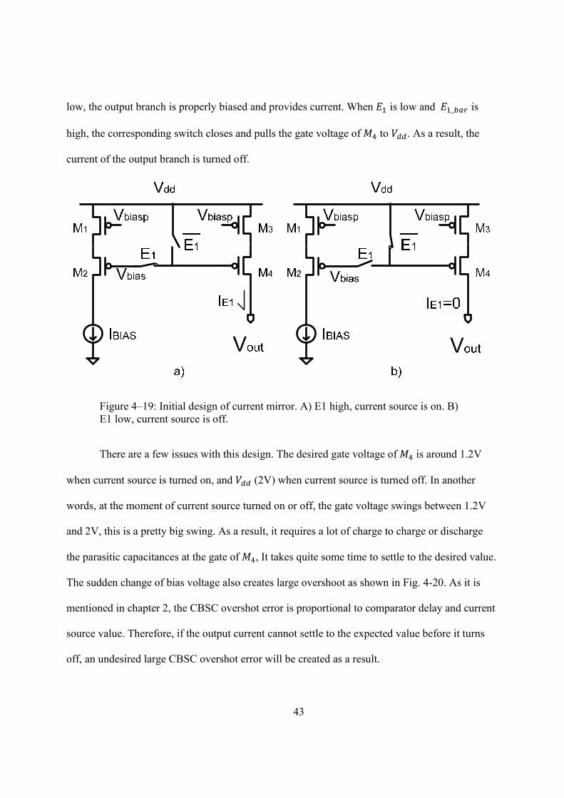
43
low, the output branch is properly biased and provides current. When is low and _ is
high, the corresponding switch closes and pulls the gate voltage of to . As a result, the
current of the output branch is turned off.
Figure 4–19: Initial design of current mirror. A) E1 high, current source is on. B) E1 low, current source is off.
There are a few issues with this design. The desired gate voltage of is around 1.2V
when current source is turned on, and (2V) when current source is turned off. In another
words, at the moment of current source turned on or off, the gate voltage swings between 1.2V
and 2V, this is a pretty big swing. As a result, it requires a lot of charge to charge or discharge
the parasitic capacitances at the gate of , It takes quite some time to settle to the desired value.
The sudden change of bias voltage also creates large overshoot as shown in Fig. 4-20. As it is
mentioned in chapter 2, the CBSC overshot error is proportional to comparator delay and current
source value. Therefore, if the output current cannot settle to the expected value before it turns
off, an undesired large CBSC overshot error will be created as a result.
44
Figure 4–20: Comparison between the ideal current source and actual current source output currents
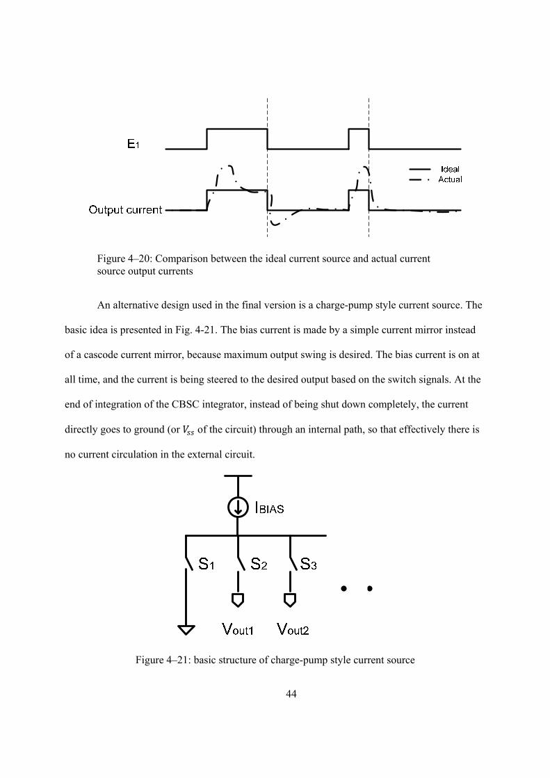
An alternative design used in the final version is a charge-pump style current source. The
basic idea is presented in Fig. 4-21. The bias current is made by a simple current mirror instead
of a cascode current mirror, because maximum output swing is desired. The bias current is on at
all time, and the current is being steered to the desired output based on the switch signals. At the
end of integration of the CBSC integrator, instead of being shut down completely, the current
directly goes to ground (or of the circuit) through an internal path, so that effectively there is
no current circulation in the external circuit.
Figure 4–21: basic structure of charge-pump style current source
45
This charge-pump style current source can reach its desired value much faster than the
switched current mirror version. Because the charge-pump style current source doesn’t change
any bias voltage of the bias current during transition, it avoids the large overshoot and long
settling time.
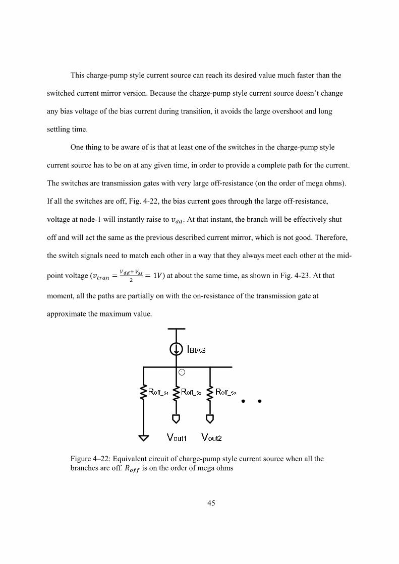
One thing to be aware of is that at least one of the switches in the charge-pump style
current source has to be on at any given time, in order to provide a complete path for the current.
The switches are transmission gates with very large off-resistance (on the order of mega ohms).
If all the switches are off, Fig. 4-22, the bias current goes through the large off-resistance,
voltage at node-1 will instantly raise to . At that instant, the branch will be effectively shut
off and will act the same as the previous described current mirror, which is not good. Therefore,
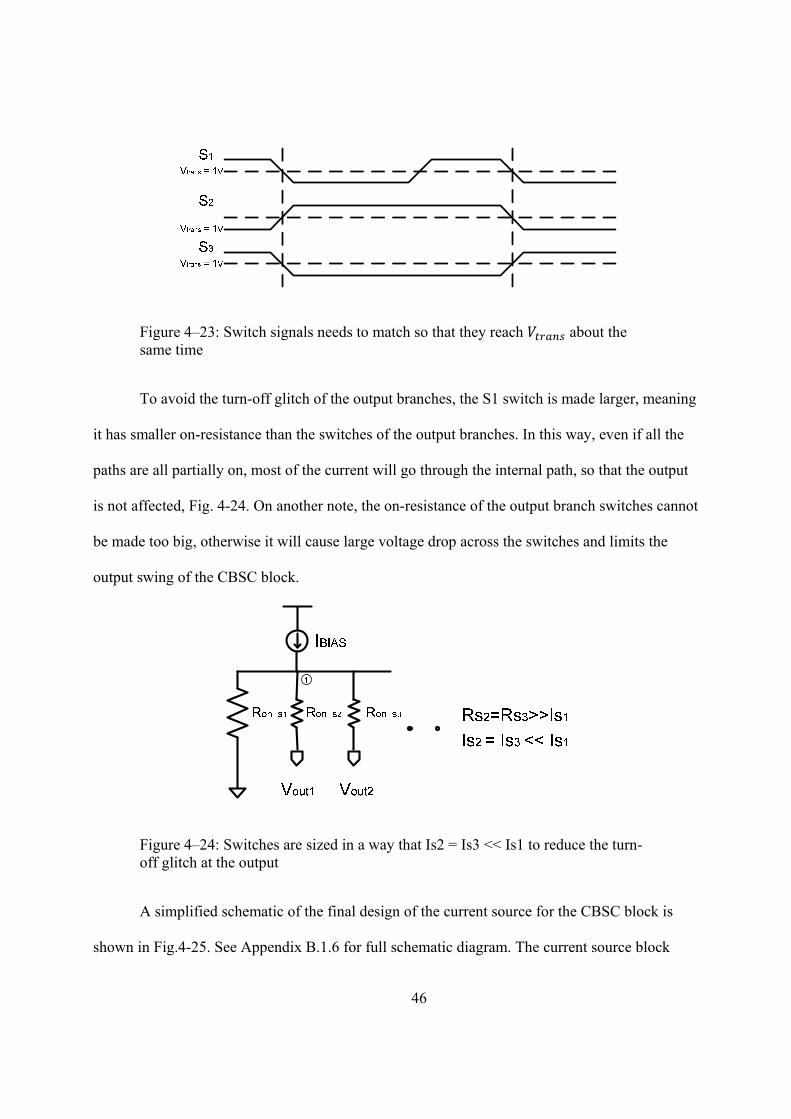
the switch signals need to match each other in a way that they always meet each other at the mid-
point voltage ( 1 ) at about the same time, as shown in Fig. 4-23. At that
moment, all the paths are partially on with the on-resistance of the transmission gate at
approximate the maximum value.
Figure 4–22: Equivalent circuit of charge-pump style current source when all the branches are off. is on the order of mega ohms
46
Figure 4–23: Switch signals needs to match so that they reach about the same time
To avoid the turn-off glitch of the output branches, the S1 switch is made larger, meaning
it has smaller on-resistance than the switches of the output branches. In this way, even if all the
paths are all partially on, most of the current will go through the internal path, so that the output
is not affected, Fig. 4-24. On another note, the on-resistance of the output branch switches cannot
be made too big, otherwise it will cause large voltage drop across the switches and limits the
output swing of the CBSC block.
Figure 4–24: Switches are sized in a way that Is2 = Is3 << Is1 to reduce the turn-off glitch at the output
A simplified schematic of the final design of the current source for the CBSC block is
shown in Fig.4-25. See Appendix B.1.6 for full schematic diagram. The current source block
47
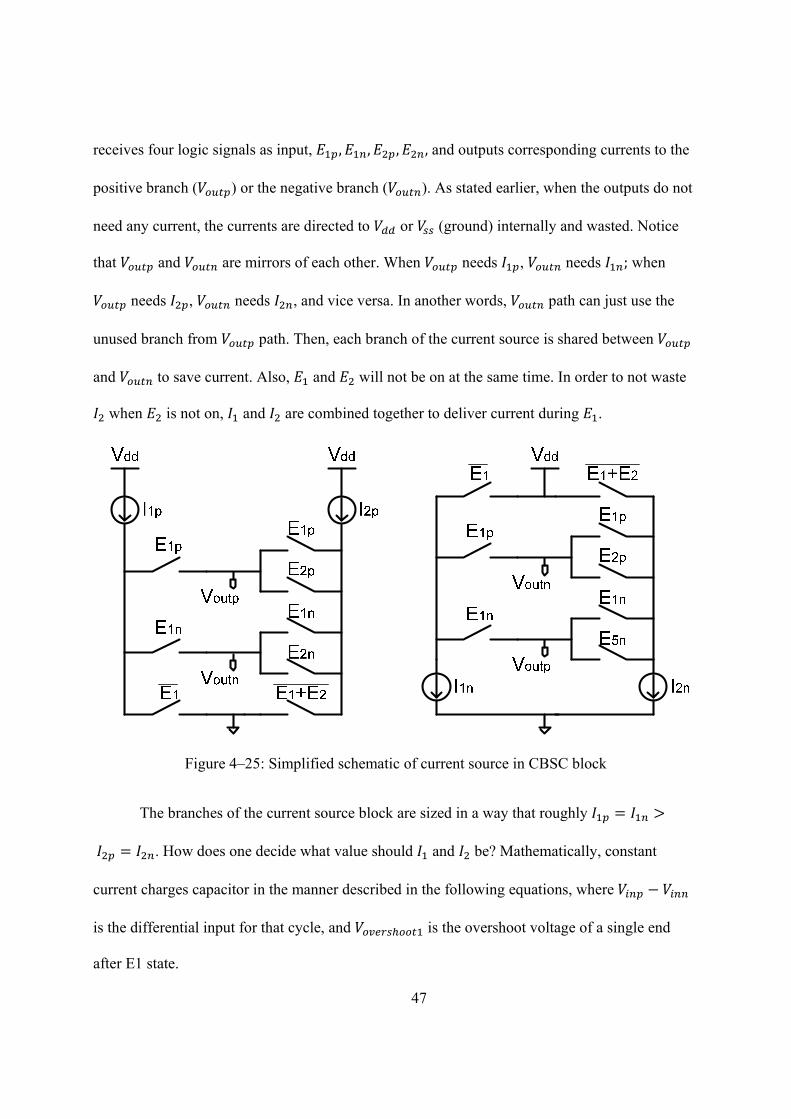
receives four logic signals as input, , , , , and outputs corresponding currents to the
positive branch ( ) or the negative branch ( ). As stated earlier, when the outputs do not
need any current, the currents are directed to or (ground) internally and wasted. Notice
that and are mirrors of each other. When needs , needs ; when
needs , needs , and vice versa. In another words, path can just use the
unused branch from path. Then, each branch of the current source is shared between
and to save current. Also, and will not be on at the same time. In order to not waste
when is not on, and are combined together to deliver current during .
Figure 4–25: Simplified schematic of current source in CBSC block
The branches of the current source block are sized in a way that roughly
. How does one decide what value should and be? Mathematically, constant
current charges capacitor in the manner described in the following equations, where
is the differential input for that cycle, and is the overshoot voltage of a single end
after E1 state.
48
| | 2 (4.11)
2 (4.12)
The goal is to find a current pair ( and ), so that integration time of each
cycle. A minimal is desired, because the size of direct affects the final overshoot voltage:
the smaller the smaller overshoot, and the better accuracy as a result. Ideally
should be almost constant for a particular comparator and a particular value. Using the largest
possible differential input for safely, one can find an estimated current pair using the above
equations. It’s only an estimate because there are a lot of non-idealities in real circuit design,
such as comparator delay is signal dependent and does not stay constant, etc. Minor tweaks are
necessary for optimal performance.
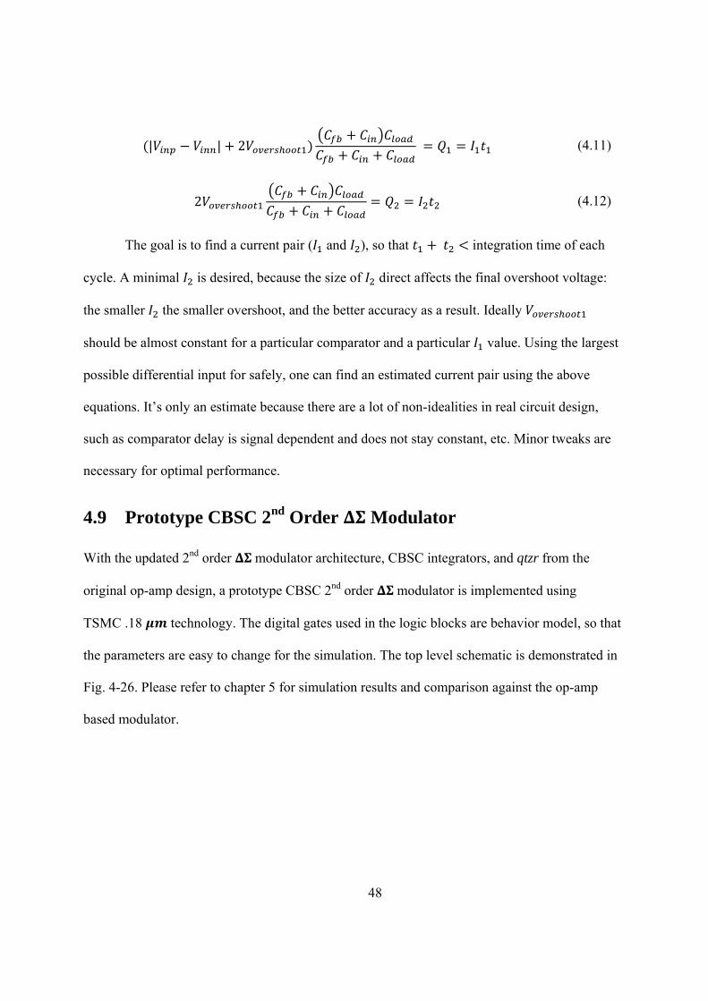
4.9 Prototype CBSC 2nd Order Modulator
With the updated 2nd order modulator architecture, CBSC integrators, and qtzr from the
original op-amp design, a prototype CBSC 2nd order modulator is implemented using
TSMC .18 technology. The digital gates used in the logic blocks are behavior model, so that
the parameters are easy to change for the simulation. The top level schematic is demonstrated in
Fig. 4-26. Please refer to chapter 5 for simulation results and comparison against the op-amp
based modulator.
49
Figure 4–26: Top level schematics of a CBSC 2nd order ΔΣ modulator
50
Chapter 5
Simulation Result
5.1 SNR
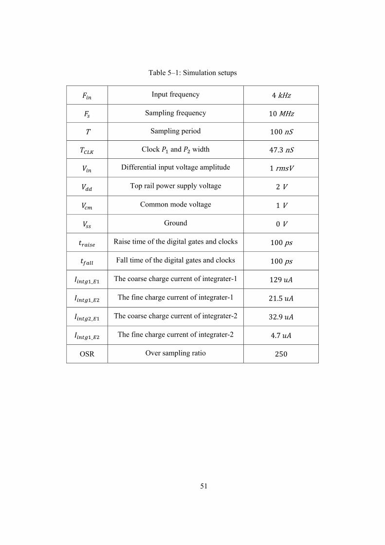
Cadence is used to simulate different versions of the modulator. The setup is in Table 5-1.
Matlab then is used to process the sum of qtzr output data and create spectrums for comparison,
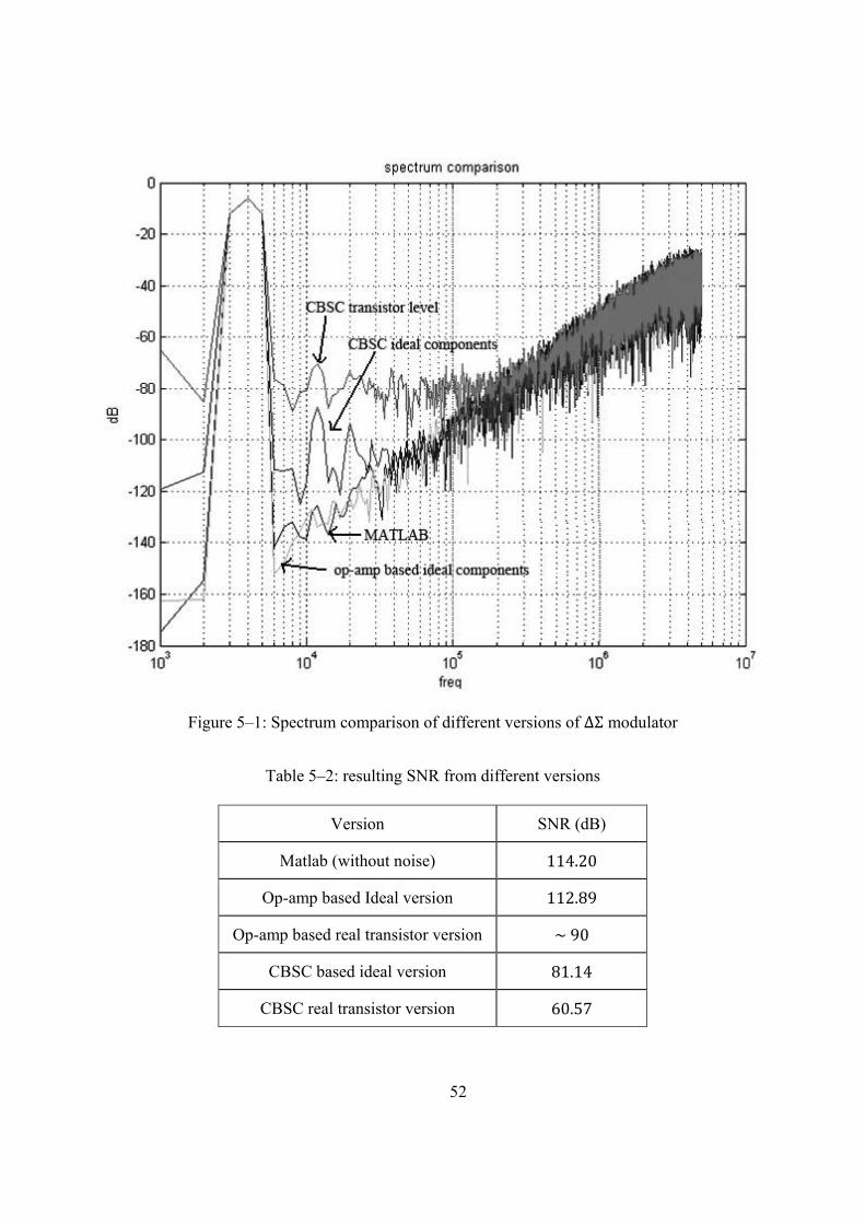
Fig. 5-1. The resulting SNR for each version is listed in Table 5-2.
The CBSC based ideal circuit version has a 30 dB drop from the mathematically
calculated noise-free result, while the op-amp based ideal circuit version can perform almost
perfectly. The reason for the performance difference is that for the ideal circuit, the op-amp gain
can be set very large and achieve almost no error. However, the logic for CBSC version is
generated using several stages of digital gates. Even though digital gates are generally very fast,
long enough delay is accumulated after several stages. As a result, overshoot error is unavoidable,
which decreases the accuracy.
The accuracy of the CBSC ΔΣ modulator is further decreased from the ideal version to
the transistor level design. The main error comes from the comparator overshoot error and delay.
The glitch caused by the on-resistance of the switch is also a factor. More careful design is
necessary to push the performance of this transistor level design.
51
Table 5–1: Simulation setups
Input frequency 4 kHz
Sampling frequency 10 MHz
T Sampling period 100 nS
Clock and width 47.3 nS
Differential input voltage amplitude 1 rmsV
Top rail power supply voltage 2 V
Common mode voltage 1 V
Ground 0 V
Raise time of the digital gates and clocks 100 ps
Fall time of the digital gates and clocks 100 ps
_ The coarse charge current of integrater-1 129
_ The fine charge current of integrater-1 21.5
_ The coarse charge current of integrater-2 32.9
_ The fine charge current of integrater-2 4.7
OSR Over sampling ratio 250
52
Figure 5–1: Spectrum comparison of different versions of ΔΣ modulator
Table 5–2: resulting SNR from different versions
Version SNR (dB)
Matlab (without noise) 114.20
Op-amp based Ideal version 112.89
Op-amp based real transistor version ~ 90
CBSC based ideal version 81.14
CBSC real transistor version 60.57

53
5.2 Power Usage
Despite the lower accuracy, the CBSC ΔΣ modulator shows a big advantage in power saving
over the op-amp based design. Table 5-2 is a comparison of the power usage and performance of
the two designs. The power usage of qtzr is not listed, because qtzr from the original op-amp
version is used for the CBSC modulator. If we use ENOB over power usage as a figure of merit
to compare the two versions, CBSC modulator shows its advantage. In this project, the CBSC
modulator is a trial version. There is lots of room for improvements. The performance should be
able to be pushed closer to ideal and achieve close to 80 dB SNR.
Table 5–3: Current usage comparison
Op-amp based CBSC based
Current Usage
Intg1 700 Current source 330.5
Comparator 33.5
Intg2 150 Current source 107.8
Comparator 28.5
Total 850 438.3
ENOB 16 bit 9.7 bit
FOM = ENOB/Power 9.41 bit/nW 11.065 bit/nW
54
Chapter 6
Conclusion
A new comparator-based switched-capacitor 2nd order ΔΣ modulator is presented. This CBSC
modulator has a number of advantages compared to the original op-amp based design.
As demonstrated in chapter 5, the CBSC modulator consumes much less power, but has
yet to match the performance of the op-amp based design. It is appropriate in applications that
have very tight power requirement but not very strict accuracy. One may argue that power and
accuracy are always a trade-off: if targeting lower accuracy, an op-amp can use less power also.
However, there is a limit. When the current is lower than a certain limit, op-amps will not settle
at all. For example, the original modulator would not be able to operate at the power level of this
CBSC modulator. Also, CBSC methodology is more amenable to design in scaled technology.
Instead of forcing the virtual ground, CBSC design detects the equal condition in an open-loop
manner, so it does not have stability issues as op-amps. Finally, CBSC is compatible with most
known architectures, with minor change.
One issue of CBSC design is discussed in section 4.2: CBSC designs can only drive
switched-capacitor loads. CBSC design cannot drive another stage directly. For those designs
that have a direct driving stage, architectural adoption is needed.
55
Chapter 7
Future Work and Ideas
Some suggestion and ideas for future work:
• An optimized design (shorter delay and low offset voltage) of the comparator in CBSC
will help increase the accuracy.
• Overshoot cancellation technique in [4] may shorten the integration time or increase
accuracy, because a smaller fine charge current can be used.
• To further save power, the current source and comparator can be turned off while they are
not being used (in idle state). However, in order to avoid possible harmful turn-on
transient behaviors, an advanced clock may need to be used to turn them on a little bit
before their outputs are supposed to be used.
• The smaller the capacitors used in the integrators the smaller the charging currents. To
further save power, one may use smaller capacitors. But be careful with the leakage
currents.
• Noise, non-ideality, and non-linearity analysis
56
Appendix A
Calculations
This appendix provides some mathematical proofs to the functionalities of CBSC circuits
discussed in this paper. The comparison between the CBSC circuits and the traditional op-amp
based circuits are demonstrated also.
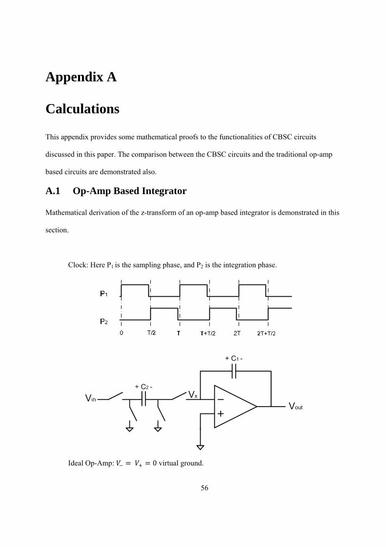
A.1 Op-Amp Based Integrator
Mathematical derivation of the z-transform of an op-amp based integrator is demonstrated in this
section.
Clock: Here P1 is the sampling phase, and P2 is the integration phase.
Ideal Op-Amp: 0 virtual ground.
57
At :
2 2 0
At :
2 2 0
2 2
At :
2
Combine the above results:
2
2
2
Z-transform:
1
1
58
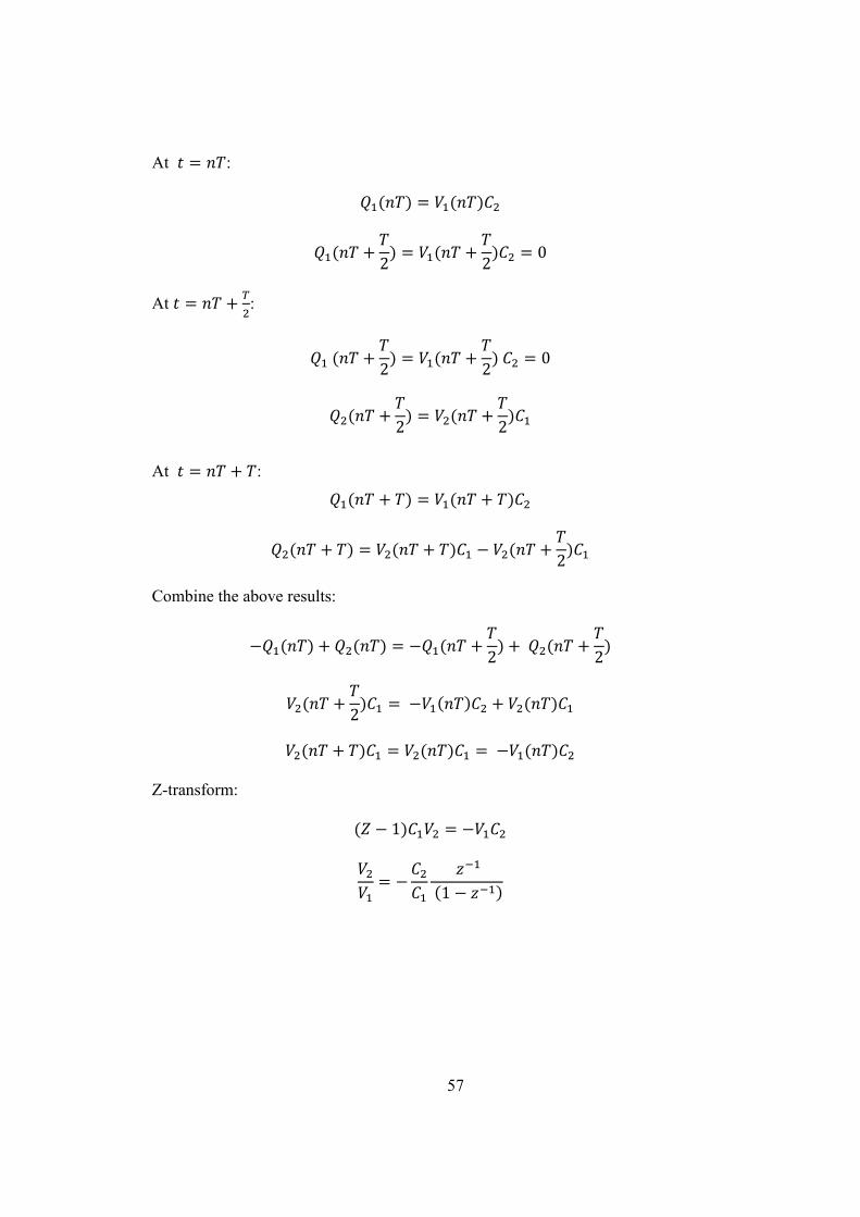
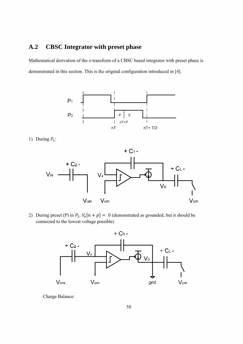
A.2 CBSC Integrator with preset phase
Mathematical derivation of the z-transform of a CBSC based integrator with preset phase is
demonstrated in this section. This is the original configuration introduced in [4].
1) During :
2) During preset (P) in : 0 (demonstrated as grounded, but it should be connected to the lowest voltage possible)
Charge Balance:
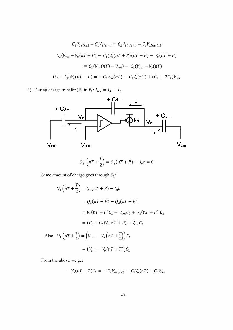
59
2
3) During charge transfer (E) in :
2 0
Same amount of charge goes through :
2
Also
From the above we get
–
60
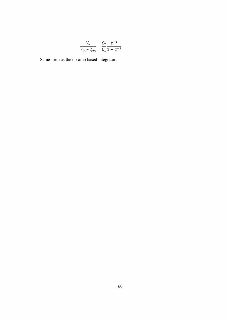
– 1
Same form as the op-amp based integrator.
61
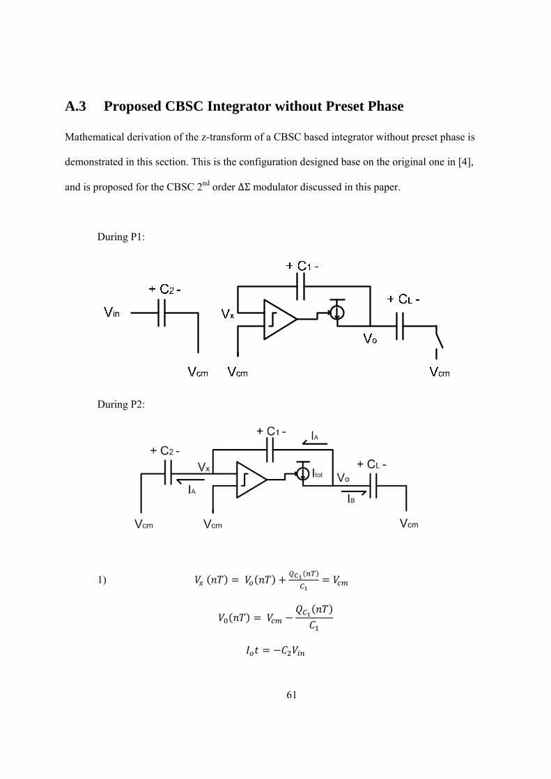
A.3 Proposed CBSC Integrator without Preset Phase
Mathematical derivation of the z-transform of a CBSC based integrator without preset phase is
demonstrated in this section. This is the configuration designed base on the original one in [4],
and is proposed for the CBSC 2nd order ΔΣ modulator discussed in this paper.
During P1:
During P2:
1)
62
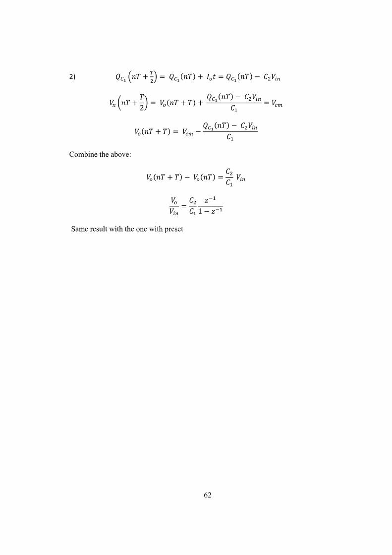
2)
2
Combine the above:
1
Same result with the one with preset
63
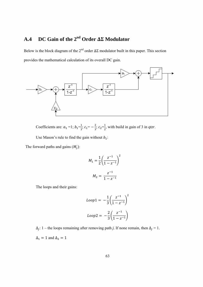
A.4 DC Gain of the 2nd Order Modulator
Below is the block diagram of the 2nd order ΔΣ modulator built in this paper. This section
provides the mathematical calculation of its overall DC gain.
Coefficients are: =1; = ; = ; = , with build in gain of 3 in qtzr.
Use Mason’s rule to find the gain without :
The forward paths and gains ( :
12 1
1
The loops and their gains:
1 13 1
2 23 1
Δ : 1 – the loops remaining after removing path j. If none remain, then Δ = 1.
Δ 1 and Δ 1
64
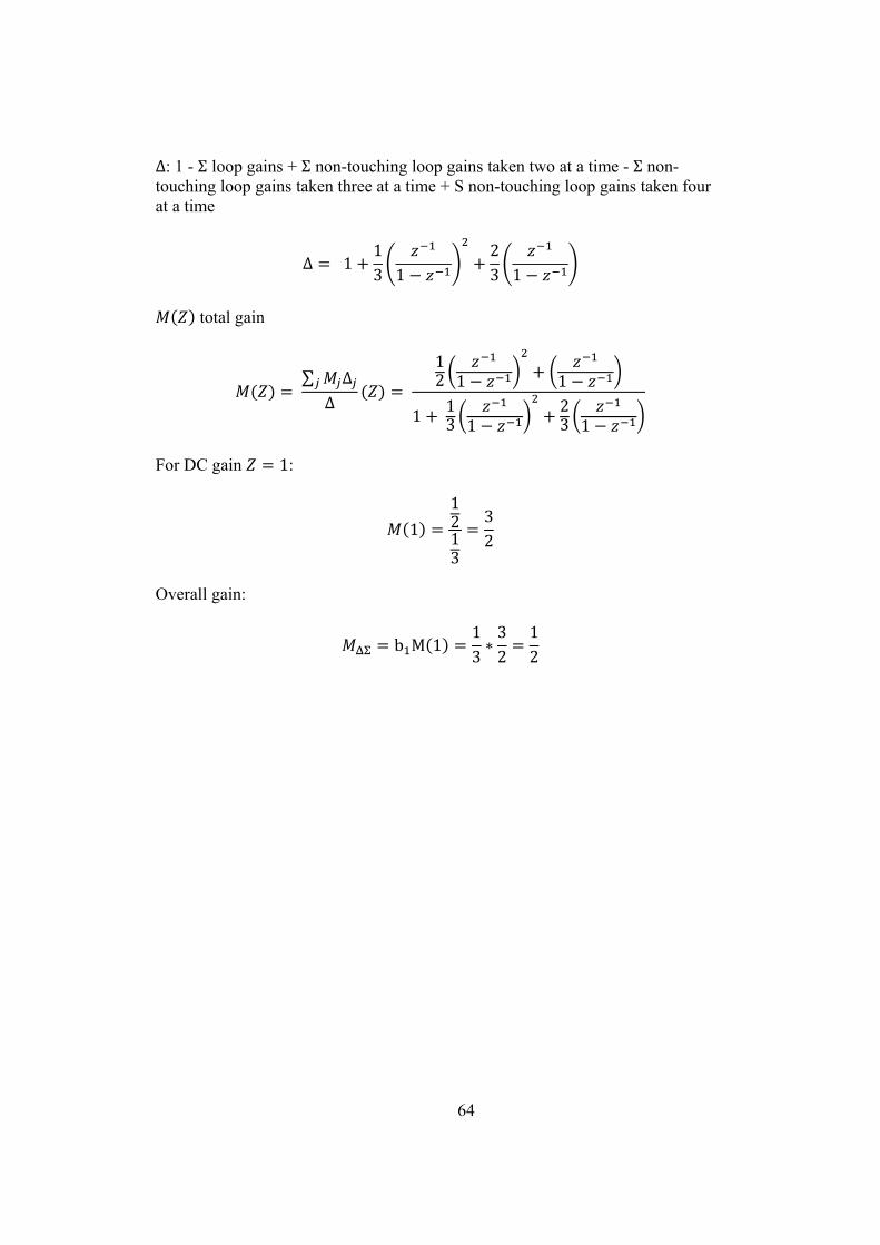
Δ: 1 - Σ loop gains + Σ non-touching loop gains taken two at a time - Σ non-touching loop gains taken three at a time + S non-touching loop gains taken four at a time
Δ 113 1
23 1
total gain
∑ Δ
Δ
12 1 1
1 13 123 1
For DC gain 1:
11213
32
Overall gain:
b M 113
32
12
65
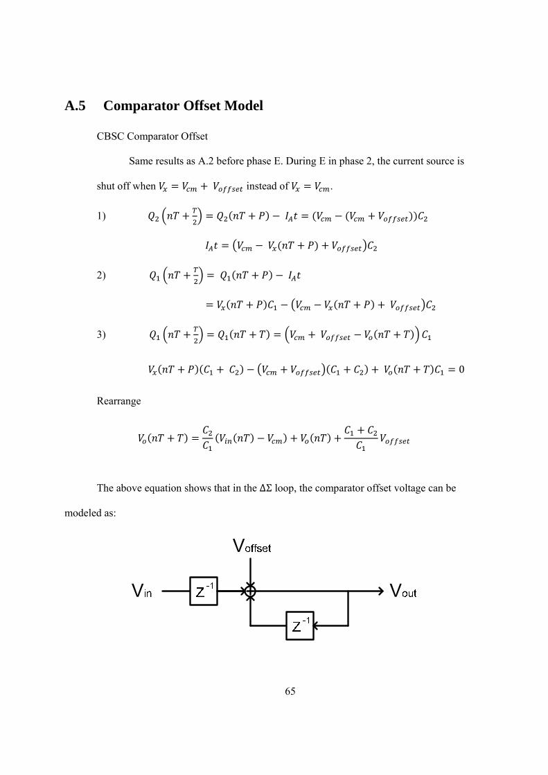
A.5 Comparator Offset Model
CBSC Comparator Offset
Same results as A.2 before phase E. During E in phase 2, the current source is
shut off when instead of .
1)
2)
3)
0
Rearrange
The above equation shows that in the ΔΣ loop, the comparator offset voltage can be
modeled as:
66
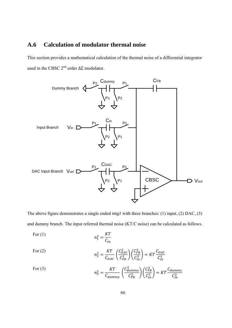
A.6 Calculation of modulator thermal noise
This section provides a mathematical calculation of the thermal noise of a differential integrator
used in the CBSC 2nd order ΔΣ modulator.
CBSC
VinP1
P1
P1
P1P2
P2
P2
P2
Cin
Cdummy CFB
Vout
Dummy Branch
Input Branch
VrefP1
P1
P2
P2
CDAC
DAC Input Branch
The above figure demonstrates a single ended intg1 with three branches: (1) input, (2) DAC, (3)
and dummy branch. The input referred thermal noise (KT/C noise) can be calculated as follows.
For (1)
For (2)
For (3)
67
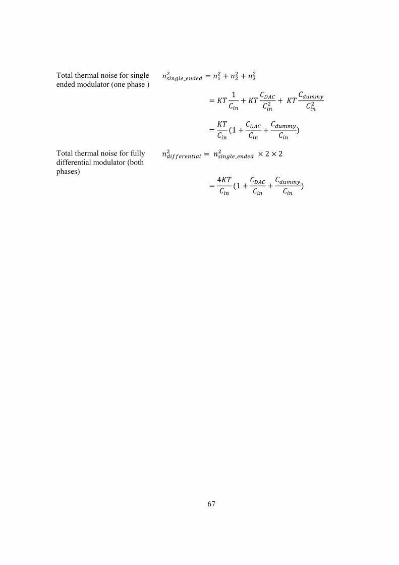
Total thermal noise for single ended modulator (one phase )
_
1
1
Total thermal noise for fully differential modulator (both phases)
_ 2 2
41
68
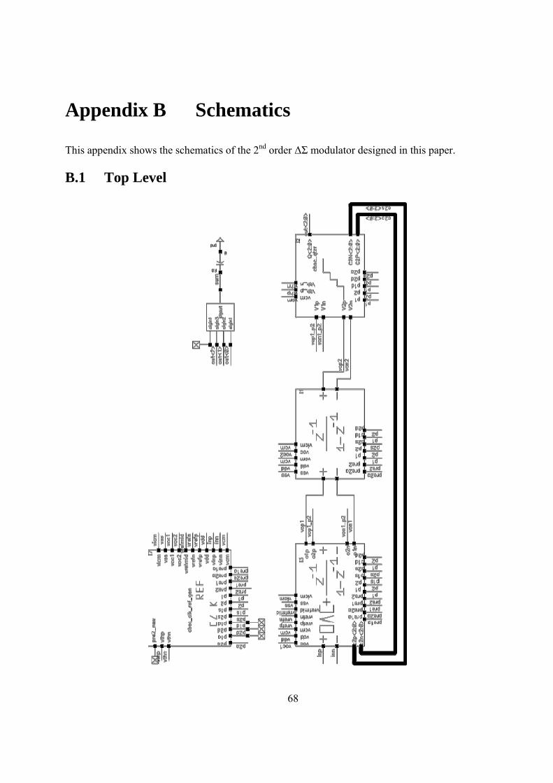
Appendix B Schematics
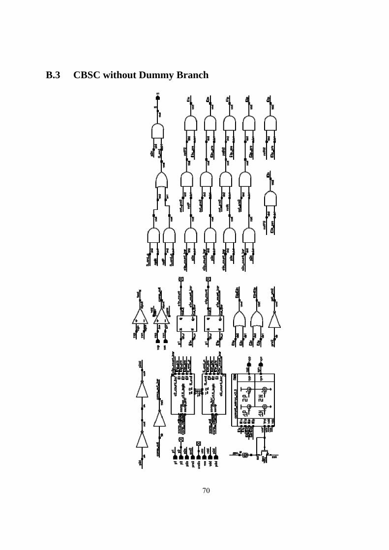
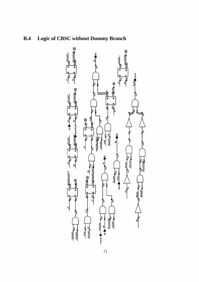
This appendix shows the schematics of the 2nd order ΔΣ modulator designed in this paper.
B.1 Top Level
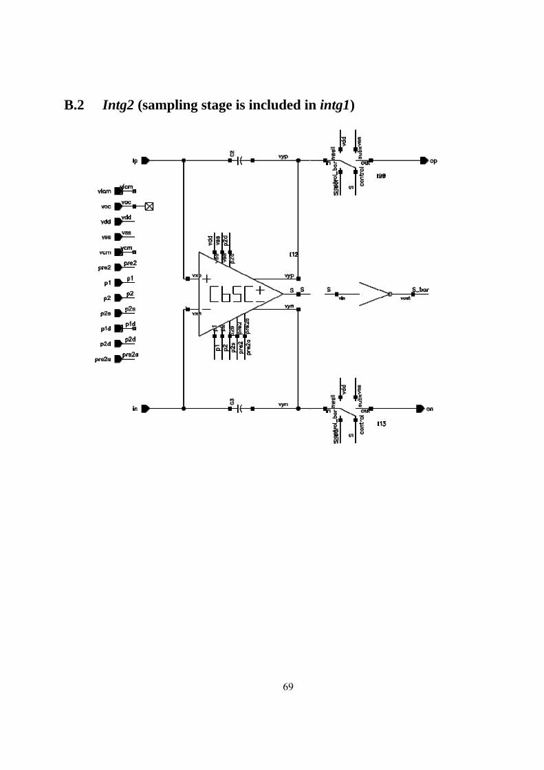
69
B.2 Intg2 (sampling stage is included in intg1)
70
B.3 CBSC without Dummy Branch
71
B.4 Logic of CBSC without Dummy Branch
72
B.5 Comparator in CBSC
73
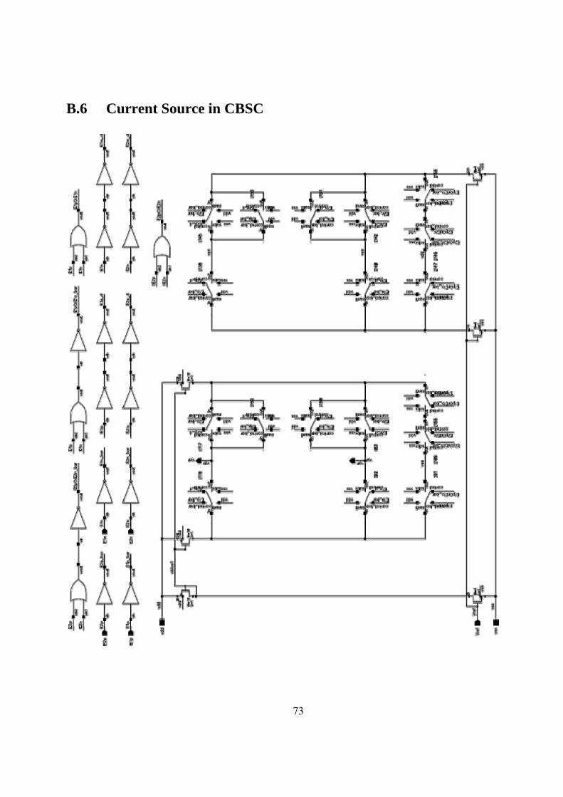
B.6 Current Source in CBSC
74
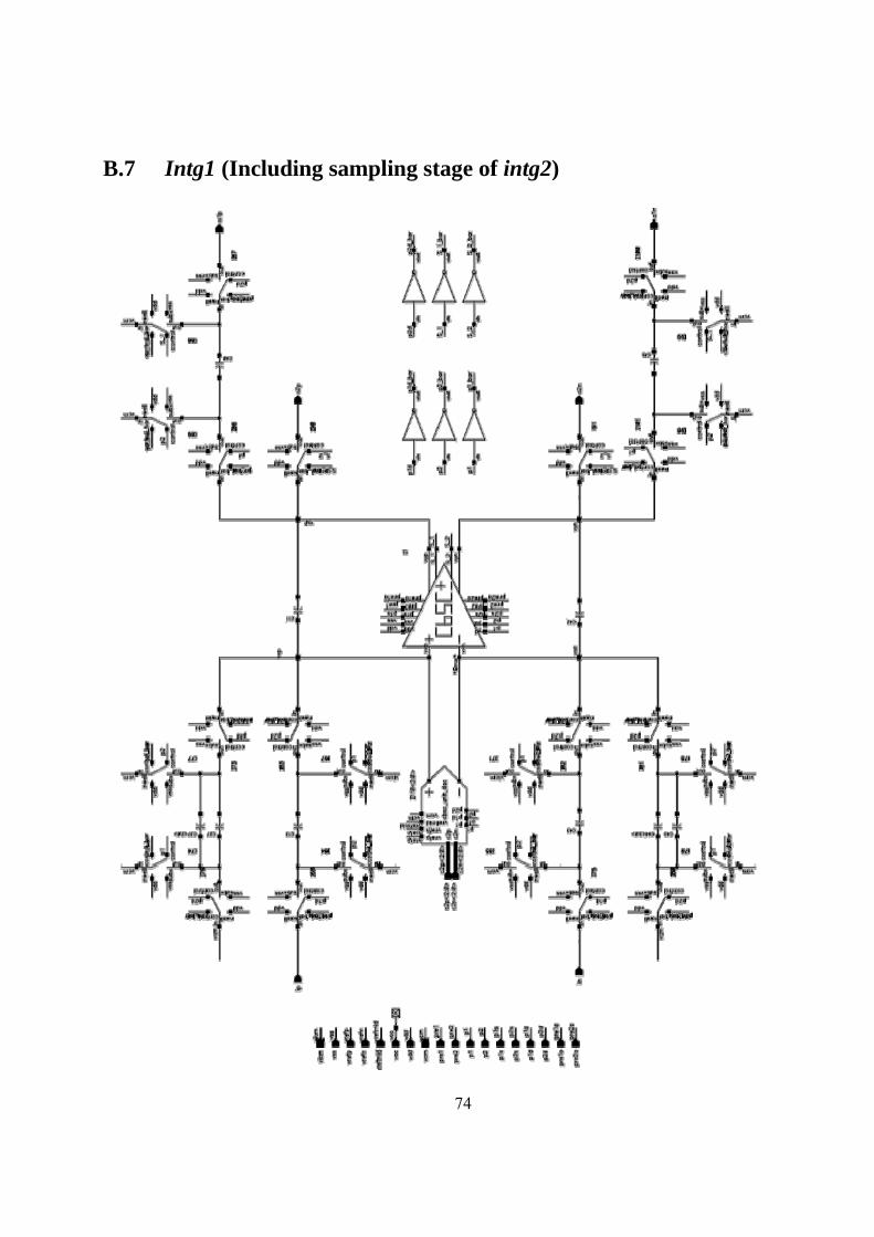
B.7 Intg1 (Including sampling stage of intg2)
75
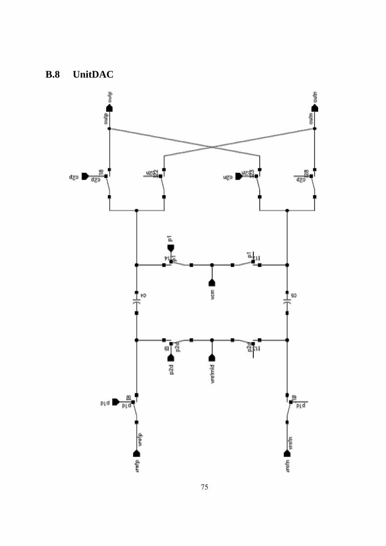
B.8 UnitDAC
76
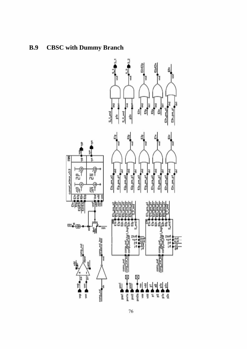
B.9 CBSC with Dummy Branch
77
B.10 Logic of CBSC with Dummy Branch
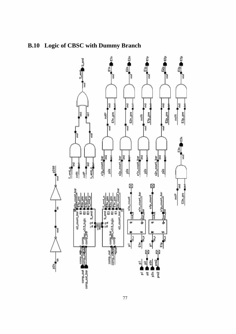
78
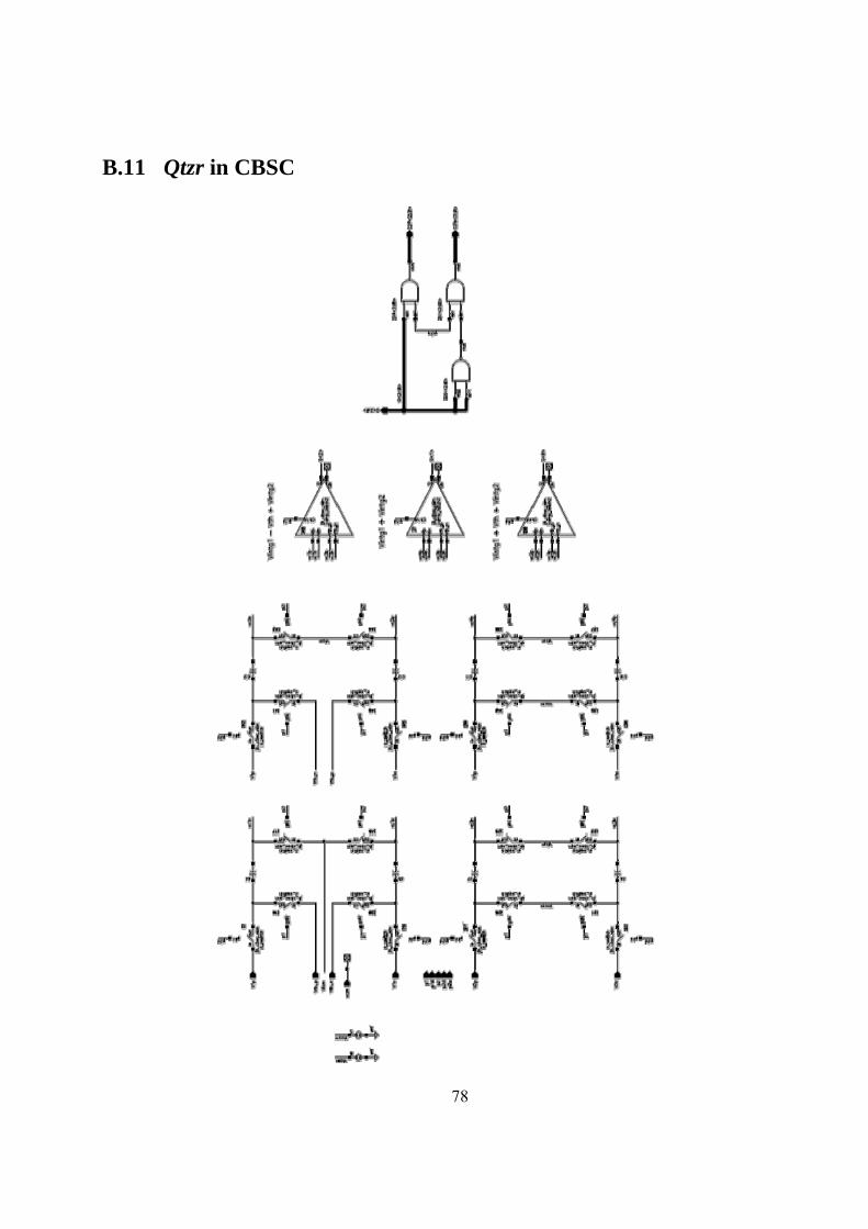
B.11 Qtzr in CBSC
79
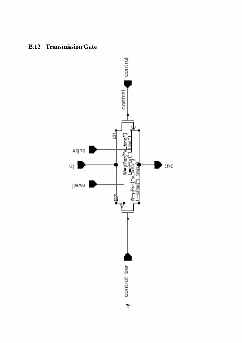
B.12 Transmission Gate
80
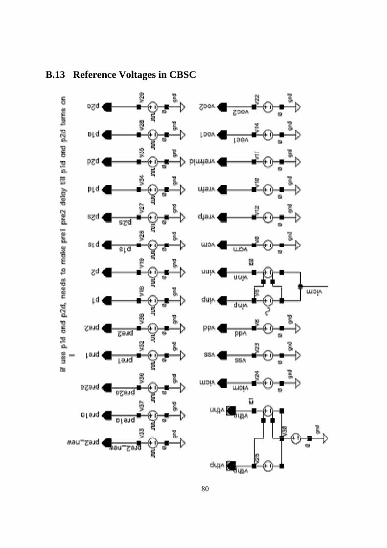
B.13 Reference Voltages in CBSC
81
Reference
[1] G. Torres, “How analog-to-digital converter (ADC) works,” [Online Document], Available HTTP: http://www.hardwaresecrets.com/article/317
[2] Z. Moussaoui and G. Miller, “Digital power control highlights,” [Online Document], Available HTTP: http://www.intersil.com/data/wp/WP0589.pdf
[3] R. Schreier and G. Temes, “Understanding delta-sigma data converters,” New Jersey: IEEE Press, 2005
[4] T Sepke, J. K. Fiorenza, C. G. Sodini, P. Holloway, and H.-S. Lee, “Comparator based switched capacitor circuits for scaled CMOS technologies” in IEEE J. Solid-State Circuits, Vol. 41, no. 12, pp. 2658-2668, Dec. 2006.
[5] M. Guyton and H.-S. Lee, “Low-voltage comparator-based switched-capacitor sigma-delta ADC” [Online Document], Available HTTP: http://mtlweb.mit.edu/research/annual_reports/2006/pdf/cs/cs_29.pdf
[6] T Sepke, J. K. Fiorenza, C. G. Sodini, P. Holloway, and H.-S. Lee, “Comparator based switched capacitor circuits for scaled CMOS technologies” in IEEE ISSCC Dig. Tech. Papers, Feb. 2006, pp. 220-221
[7] Katanzag, “Delta-sigma modulation” [Online document], 2006, Available HTTP: http://en.wikipedia.org/wiki/Flip-flop_(electronics)
[8] Mano, M. Morris; Kime, Charles R, Logic and Computer Design Fundamentals, 3rd Edition. Upper Saddle River, NJ, USA: Pearson Education International. pp. pg283. ISBN 0-13-1911651.
[9] Todd C. Sepke, “Comparator Design and Analysis for Comparator-Based Switched-Capacitor Circuits”, 2006, MIT internal thesis collection
[10] M. Momeni, D. Prelog, B. Horvat, M. Glesner, “Comparator-Based Switched-Capacitor, Delta-Sigma Modulation”, in Contemporary Engineering Sciences, Vol. 1, 2008, no. 1, 1 - 13