Embed Size (px)
Citation preview

Eduardo José Resende Ortigueira Licenciatura em Ciências da Engenharia Electrotécnica e de
Computadores
A Combined LNA-Oscillator-Mixer For Biomedical Applications
Dissertação para obtenção do Grau de Mestre em Engenharia Electrotécnica e de Computadores
Orientador: Prof. Doutor Luís Augusto Bica Gomes de Oliveira
Júri:
Presidente: Prof. Doutor João Carlos de Palma Goes Arguente: Prof. Doutor João Pedro Abreu de Oliveira
Vogal: Prof. Doutor Jorge Manuel dos Santos Ribeiro Fernandes
Novembro 2011


Copyright
A Combined LNA-Oscillator-Mixer For Biomedical Applications
Eduardo José Resende Ortigueira - Todos os direitos reservados.
A Faculdade de Ciências e Tecnologia e a Universidade Nova de Lisboa têm o direito, perpétuo e
sem limites geográcos, de arquivar e publicar esta dissertação através de exemplares impressos
reproduzidos em papel ou de forma digital, ou por qualquer outro meio conhecido ou que venha
a ser inventado, e de a divulgar através de repositórios cientícos e de admitir a sua cópia e
distribuição com objectivos educacionais ou de investigação, não comerciais, desde que seja dado
crédito ao autor e editor.
III


Dedicated to my family, friends and girlfriend. . .
V


Acknowledgements
First I would like to address a special appreciation to the Department of Electrical Engineering
of the Faculty of Science and Technology as a learning and research infrastructure. It provides,
to all its students, large experience and knowledge under strong and friendly guidance and over
a nice working atmosphere and support throughout their academic pursuits. I could not think
of a better place to start this important journey of my life and I am sincerely glad for having
attended this institution. I am also thankful to many professors I have met across my academic
journey, specially Prof. Adolfo Steiger Garção, Prof. João Carlos Goes, Prof. Nuno Paulino and
Prof. João Pedro Oliveira for introducing me to the amazing world of electronics.
However I want to express my particular gratitude for the person, who perhaps, was the main
responsible for this thesis been done, my advisor, Prof. Luís Oliveira specially due to the single
and unique working environment he provides for all his students. Not for one second he showed
lack of commitment and dedication and I am strongly aware that his guidance and support was
priceless and fundamental for me to grow as a student and as a researcher
I would also like to gratefully acknowledge dear appreciation to my oce colleagues Arito Melo,
Hugo Lopes, Ivan Bastos, João Pacheco, Leonardo Canha and Tiago Brito for all the technical
advices, working atmosphere and fellowship they provided while doing this thesis.
During the time I spent in college I met also great co-workers that eventually became close
friends and whom I shared many good moments and whom I look forward to calling each of
them friends and colleagues for many years to come. For Frederico Gonçalves, Miguel Oliveira
and Paulo Figueiras also a dedicated thanks.
However many other contributed for the successful ending of one of the most important chapters
of my life. I want to present my gratitude to all of them. First a thanks to my friends António
Seixas, Daniel Bernardo, José Belo, Ricardo Bernardino and Tiago Lobo for being the best friends
I could wish for. Second but not least I want to thank my mother Laurinda Ortigueira, my father
Manuel Ortigueira and my sister Joana Ortigueira for the endless love, patience, understanding
and for encountering always means to motivate me and lead me into right directions and for giving
me unconditional support even when there were times where I was not worthy of such. Finally I
would like to thank my girlfriend, Guida Pereira, for being of the most important cornerstones
of my life. I want to say that each and everyone of you can share in my accomplishment. This
work is dedicated to all of you, knowing that without your support none of this would have been
possible.
VII


UNIVERSIDADE NOVA DE LISBOA
Resumo
Faculdade de Ciências e Tecnologia
Departamento de Engenharia Electrotécnica e de Computadores
Mestrado em Engenharia Electrotécnica e de Computadores
por
Nesta tese um LNA-Oscilador-Misturador, o LOM, é apresentado. Este circuito combinado é
possível devido á exploração do comportamento não linear de um oscilador Two-Integrator. A
metodologia de projecto utilizada possui algumas vantagens visto que reduz signicantemente o
número de transistores ao mesmo tempo que possibilita reutilização de corrente. O resultado é
um front-end de RF de tamanho reduzido, baixo custo e baixo consumo de potência. Um andar
de common-gate é utilizado para implementação do amplicador de baixo ruído o que torna o
circuito apresentado capaz de cobrir as bandas de frequência WMTS, desde os 600 MHz até aos
1.4 GHz. O sistema foi totalmente implementado com MOSFETs sem uso de elementos reactivos
e um protótipo do circuito, utilizando tecnologia UMC CMOS de 130 nm, é apresentado. Técni-
cas simples e qualitativas são utilizadas, tanto no design como na optimização, a qual tendo em
vista as redução de área e de potência consumida, sem atenção especial por outras medidas de
performance. O circuito apresenta um consumo total de 8.2 mW, extraídos de uma fonte de 1.2
V, e uma área de 110.96x92.32 µm2.
Palavras-chave: Circuitos MOSFET-only, Oscilador Two-integrator, Osciladores em Quadratura,
Receptores Low-IF, Misturadores Activos, LNA-Oscilador-Misturador Combinado.
IX


UNIVERSIDADE NOVA DE LISBOA
Abstract
Faculdade de Ciências e Tecnologia
Departamento de Engenharia Electrotécnica e de Computadores
Mestrado em Engenharia Electrotécnica e de Computadores
by
In this thesis a combined LNA-oscillator-mixer, the LOM, is presented. This combined circuit
is possible by exploiting the Non-Linear Behavior of a Two-Integrator oscillator. This design
approach has some advantages since it lowers signicantly the number of transistors used as well
as it allows current reuse. The result is a low size, low cost and low power RF front-end. A
common-gate stage is used to implement the LNA, which turns the circuit capable to cover the
WMTS frequency bands from 600 MHz to 1.4 GHz. The system is a MOSFET only circuit im-
plemented without any reactive components and a circuit prototype using UMC 130 nm CMOS
technology is presented. Simple and qualitative techniques are used to design and optimize the
circuit for power consumption and area understate with no special regards about other measure-
ments of performance. The circuit has an overall consumption of 8.2 mW drawn from a 1.2 V
supply and an area of 110.96x92.32 µm2.
Keywords: MOSFET-only Circuits, Two-integrator Oscillator, Quadrature Oscillators, Low-IF
Receivers, Active Mixers, Combined LNA-Oscillator-Mixer.
XI


Contents
Copyright III
Acknowledgements VII
Resumo IX
Abstract XI
List of Figures XV
List of Tables XIX
Abbreviations XXI
1 Introduction 1
1.1 Background and Motivation . . . . . . . . . . . . . . . . . . . . . . . . . . . . . . 1
1.2 Thesis Organization . . . . . . . . . . . . . . . . . . . . . . . . . . . . . . . . . . 3
1.3 Main Contributions . . . . . . . . . . . . . . . . . . . . . . . . . . . . . . . . . . . 4
2 Receiver Architectures and RF Blocks 5
2.1 Receiver Architectures . . . . . . . . . . . . . . . . . . . . . . . . . . . . . . . . . 5
2.1.1 Heterodyne Receiver . . . . . . . . . . . . . . . . . . . . . . . . . . . . . . 6
2.1.2 Homodyne receiver . . . . . . . . . . . . . . . . . . . . . . . . . . . . . . . 8
2.1.3 Low IF receivers . . . . . . . . . . . . . . . . . . . . . . . . . . . . . . . . 8
2.2 CMOS Implementation Basic Concepts . . . . . . . . . . . . . . . . . . . . . . . . 10
2.2.1 Gain . . . . . . . . . . . . . . . . . . . . . . . . . . . . . . . . . . . . . . . 10
2.2.2 Input Impedance . . . . . . . . . . . . . . . . . . . . . . . . . . . . . . . . 12
2.2.3 Noise . . . . . . . . . . . . . . . . . . . . . . . . . . . . . . . . . . . . . . . 14
2.2.3.1 Thermal Noise . . . . . . . . . . . . . . . . . . . . . . . . . . . . 14
2.2.3.2 Flicker Noise . . . . . . . . . . . . . . . . . . . . . . . . . . . . . 15
2.2.3.3 Noise Factor . . . . . . . . . . . . . . . . . . . . . . . . . . . . . 16
2.2.4 Linearity . . . . . . . . . . . . . . . . . . . . . . . . . . . . . . . . . . . . 17
2.2.4.1 1 dB Compression Point . . . . . . . . . . . . . . . . . . . . . . . 18
2.2.4.2 Intermodulation Distortion . . . . . . . . . . . . . . . . . . . . . 18
2.3 CMOS Common Gate Stage . . . . . . . . . . . . . . . . . . . . . . . . . . . . . . 20
2.4 CMOS Dierential Pair . . . . . . . . . . . . . . . . . . . . . . . . . . . . . . . . 22
2.5 Mixers . . . . . . . . . . . . . . . . . . . . . . . . . . . . . . . . . . . . . . . . . . 25
2.5.1 Mixer Concepts . . . . . . . . . . . . . . . . . . . . . . . . . . . . . . . . . 26
XIII

Contents
2.5.2 Passive Mixer . . . . . . . . . . . . . . . . . . . . . . . . . . . . . . . . . . 28
2.5.3 Active Mixers . . . . . . . . . . . . . . . . . . . . . . . . . . . . . . . . . . 29
2.6 Oscillators . . . . . . . . . . . . . . . . . . . . . . . . . . . . . . . . . . . . . . . . 31
2.6.1 Oscillator Basic Concepts . . . . . . . . . . . . . . . . . . . . . . . . . . . 31
2.6.1.1 Barkhausen Criterium . . . . . . . . . . . . . . . . . . . . . . . . 31
2.6.1.2 Phase Noise . . . . . . . . . . . . . . . . . . . . . . . . . . . . . . 32
2.6.1.3 Quality Factor . . . . . . . . . . . . . . . . . . . . . . . . . . . . 34
2.6.1.4 Quadrature Outputs . . . . . . . . . . . . . . . . . . . . . . . . . 35
2.6.2 LC Oscillators . . . . . . . . . . . . . . . . . . . . . . . . . . . . . . . . . 36
2.6.3 RC Oscillators . . . . . . . . . . . . . . . . . . . . . . . . . . . . . . . . . 37
3 Single Balanced Mixer and Gilbert Cell 39
3.1 Introduction . . . . . . . . . . . . . . . . . . . . . . . . . . . . . . . . . . . . . . . 39
3.2 Voltage Conversion Gain . . . . . . . . . . . . . . . . . . . . . . . . . . . . . . . . 41
3.3 Noise Analysis . . . . . . . . . . . . . . . . . . . . . . . . . . . . . . . . . . . . . 47
3.3.1 Switching Pair Average Transconductance . . . . . . . . . . . . . . . . . . 47
3.3.2 Single Balanced Mixer Noise Factor . . . . . . . . . . . . . . . . . . . . . 48
3.4 MOSFET-Only Gilbert Cell Simulation . . . . . . . . . . . . . . . . . . . . . . . 52
4 Two Integrator Oscillator 61
4.1 Introduction . . . . . . . . . . . . . . . . . . . . . . . . . . . . . . . . . . . . . . . 61
4.2 Barkhausen Criterion . . . . . . . . . . . . . . . . . . . . . . . . . . . . . . . . . . 64
4.2.1 Phase Condition . . . . . . . . . . . . . . . . . . . . . . . . . . . . . . . . 64
4.2.2 Gain Condition . . . . . . . . . . . . . . . . . . . . . . . . . . . . . . . . . 66
4.3 Linear Model and Carrier Characterization . . . . . . . . . . . . . . . . . . . . . 69
4.4 Two Integrator Oscillator Behaviors . . . . . . . . . . . . . . . . . . . . . . . . . 70
4.4.1 Linear Behavior . . . . . . . . . . . . . . . . . . . . . . . . . . . . . . . . . 71
4.4.2 Non-Linear Behavior . . . . . . . . . . . . . . . . . . . . . . . . . . . . . . 72
4.4.3 Simulation and Discussion . . . . . . . . . . . . . . . . . . . . . . . . . . . 74
5 LOM Design and Simulation 79
5.1 Introduction . . . . . . . . . . . . . . . . . . . . . . . . . . . . . . . . . . . . . . . 79
5.2 Low Noise Amplier Validation And Discussion . . . . . . . . . . . . . . . . . . . 81
5.3 Combined LNA-Oscillator-Mixer . . . . . . . . . . . . . . . . . . . . . . . . . . . 86
6 Conclusion and Future Work 101
6.1 Conclusion . . . . . . . . . . . . . . . . . . . . . . . . . . . . . . . . . . . . . . . . 101
6.2 Future Work . . . . . . . . . . . . . . . . . . . . . . . . . . . . . . . . . . . . . . 104
A Trapezoid Wave Fourier Expansion And Time Description 109
B Published Paper And Award 117
XIV

List of Figures
2.1 Heterodyne Receiver . . . . . . . . . . . . . . . . . . . . . . . . . . . . . . . . . . 7
2.2 Image Problem in Heterodyne Receiver . . . . . . . . . . . . . . . . . . . . . . . . 7
2.3 Quadrature Homodyne Receiver . . . . . . . . . . . . . . . . . . . . . . . . . . . . 8
2.4 Low IF Receiver With Hartley Image rejection Architecture . . . . . . . . . . . . 9
2.5 Low IF Receiver With Weaver Image Rejection . . . . . . . . . . . . . . . . . . . 10
2.6 MOSFET Model and Operation Regions . . . . . . . . . . . . . . . . . . . . . . . 11
2.7 MOS Saturation Region I-V Curve And Transconductance Determination . . . . 11
2.8 Body Eect Demonstrated Using Small Signal Analysis . . . . . . . . . . . . . . . 12
2.9 Input Impedance Using Thevenin Model . . . . . . . . . . . . . . . . . . . . . . . 13
2.10 Resistor Thermal Noise Model . . . . . . . . . . . . . . . . . . . . . . . . . . . . . 14
2.11 Power Spectrum of Flicker Noise And Thermal Noise . . . . . . . . . . . . . . . . 15
2.12 MOSFET Flicker Noise Model . . . . . . . . . . . . . . . . . . . . . . . . . . . . . 16
2.13 Noisy Diport . . . . . . . . . . . . . . . . . . . . . . . . . . . . . . . . . . . . . . 16
2.14 1dB Compression Point . . . . . . . . . . . . . . . . . . . . . . . . . . . . . . . . 18
2.15 CG Stage and Small Signal Model . . . . . . . . . . . . . . . . . . . . . . . . . . 20
2.16 Common Gate Small Signal Model With Noise Sources . . . . . . . . . . . . . . . 21
2.17 Common Source Stage and CMOS Dierential Pair . . . . . . . . . . . . . . . . . 22
2.18 CMOS Dierential Pair Current Balance . . . . . . . . . . . . . . . . . . . . . . . 23
2.19 Common Source Stage Small Signal Model . . . . . . . . . . . . . . . . . . . . . . 24
2.20 Basic Mixing Operation . . . . . . . . . . . . . . . . . . . . . . . . . . . . . . . . 25
2.21 Down-Conversion Resulting Spectrum . . . . . . . . . . . . . . . . . . . . . . . . 26
2.22 IIP3 Determination . . . . . . . . . . . . . . . . . . . . . . . . . . . . . . . . . . . 28
2.23 Passive Mixer Using Active Device . . . . . . . . . . . . . . . . . . . . . . . . . . 29
2.24 Single Balanced Mixer . . . . . . . . . . . . . . . . . . . . . . . . . . . . . . . . . 30
2.25 Gilbert Cell . . . . . . . . . . . . . . . . . . . . . . . . . . . . . . . . . . . . . . . 30
2.26 Simple Feedback System . . . . . . . . . . . . . . . . . . . . . . . . . . . . . . . . 31
2.27 Ideal Carrier and Carrier With Phase-Noise . . . . . . . . . . . . . . . . . . . . . 32
2.28 Phase-Noise Eect in Down-Conversion . . . . . . . . . . . . . . . . . . . . . . . 33
2.29 Phase-Noise SSB . . . . . . . . . . . . . . . . . . . . . . . . . . . . . . . . . . . . 33
2.30 Carrier Spectrum Regarding Variations in The Quality Factor . . . . . . . . . . . 34
2.31 LC Oscillator . . . . . . . . . . . . . . . . . . . . . . . . . . . . . . . . . . . . . . 36
2.32 LC Oscillator Linear Model . . . . . . . . . . . . . . . . . . . . . . . . . . . . . . 36
2.33 Relaxation Oscillator . . . . . . . . . . . . . . . . . . . . . . . . . . . . . . . . . . 37
3.1 Single-Balanced Mixer . . . . . . . . . . . . . . . . . . . . . . . . . . . . . . . . . 40
3.2 LO Signal . . . . . . . . . . . . . . . . . . . . . . . . . . . . . . . . . . . . . . . . 41
3.3 Typical Dierential Pair Responses . . . . . . . . . . . . . . . . . . . . . . . . . . 43
XV

List of Figures
3.4 Ideal First and Second Order Responses Of The Dierential Pair . . . . . . . . . 44
3.5 Reference Square and Triangular Wave . . . . . . . . . . . . . . . . . . . . . . . . 44
3.6 p1(t) Fourier Coecients . . . . . . . . . . . . . . . . . . . . . . . . . . . . . . . . 45
3.7 Single Balanced Mixer With CG Stage . . . . . . . . . . . . . . . . . . . . . . . . 46
3.8 Dierential Pair I-V Characteristic and Equivalent Transconductance . . . . . . . 47
3.9 Non-Zero Transconductance . . . . . . . . . . . . . . . . . . . . . . . . . . . . . . 48
3.10 Wideband Gilbert Cell . . . . . . . . . . . . . . . . . . . . . . . . . . . . . . . . . 53
3.11 Biasing Resistors Implemented With Active Loads . . . . . . . . . . . . . . . . . 53
3.12 MOSFET-only Gilbert Cell Design Orientation . . . . . . . . . . . . . . . . . . . 54
3.13 Switching Pair Current Characteristic Degeneration . . . . . . . . . . . . . . . . . 55
3.14 MOSFET-only Gilbert Cell Design Values . . . . . . . . . . . . . . . . . . . . . . 55
3.15 Gilbert Cell Conversion Gain And Noise Factor Curves . . . . . . . . . . . . . . . 57
3.16 Simulated Conversion Gain and NF as a Function Of the Load Transistor Width 57
3.17 Gilbert Cell IIP3 . . . . . . . . . . . . . . . . . . . . . . . . . . . . . . . . . . . . 59
3.18 Switching Pair Current Characteristic in the Optimal Point . . . . . . . . . . . . 59
4.1 CMOS Two-Integrator Oscillator . . . . . . . . . . . . . . . . . . . . . . . . . . . 62
4.2 Two-Integrator Capacitor . . . . . . . . . . . . . . . . . . . . . . . . . . . . . . . 63
4.3 Capacitor Charge in The Two-Integrator Oscillator . . . . . . . . . . . . . . . . . 63
4.4 Steady State Oscillations . . . . . . . . . . . . . . . . . . . . . . . . . . . . . . . . 64
4.5 Direct Coupling in the Two-Integrator Oscillator . . . . . . . . . . . . . . . . . . 65
4.6 Cross Coupling in the Two-Integrator Oscillator . . . . . . . . . . . . . . . . . . . 66
4.7 Cross-Coupled Dierential Pair . . . . . . . . . . . . . . . . . . . . . . . . . . . . 67
4.8 Small Signal Analysis of Cross-Coupled Dierential Pair . . . . . . . . . . . . . . 67
4.9 Amplitude Stabilization . . . . . . . . . . . . . . . . . . . . . . . . . . . . . . . . 68
4.10 Transistor Variable Transconductance and Dierential Pair Periodic Transconduc-tance . . . . . . . . . . . . . . . . . . . . . . . . . . . . . . . . . . . . . . . . . . . 69
4.11 Linear Model of the Two-Integrator Oscillator . . . . . . . . . . . . . . . . . . . . 69
4.12 Currents Produced by the Dierential Pair and Regions of Operation . . . . . . . 71
4.13 High Level Model in Linear Behavior . . . . . . . . . . . . . . . . . . . . . . . . . 71
4.14 Two-Integrator Output Waveform in Linear Behavior . . . . . . . . . . . . . . . . 72
4.15 High Level Model in Non-Linear Behavior . . . . . . . . . . . . . . . . . . . . . . 73
4.16 Two-Integrator Output Waveform in A Non-Linear Behavior . . . . . . . . . . . . 73
4.17 MOSFET-only Two-Integrator . . . . . . . . . . . . . . . . . . . . . . . . . . . . 74
4.18 Two-Integrator Design Values . . . . . . . . . . . . . . . . . . . . . . . . . . . . . 75
4.19 MOSFET-only Two-Integrator Parameters and Simulation Results . . . . . . . . 76
4.20 Two-Integrator Switching Pair Current Characteristics . . . . . . . . . . . . . . . 76
4.21 Two-Integrator Switching Pair Optimal Current Characteristics . . . . . . . . . . 77
5.1 Single Balanced Mixer Structure in the Two Integrator Oscillator . . . . . . . . . 80
5.2 Common-Source Stage Impedance Matching . . . . . . . . . . . . . . . . . . . . . 82
5.3 Balun LNA . . . . . . . . . . . . . . . . . . . . . . . . . . . . . . . . . . . . . . . 82
5.4 Balun Connection Possibilities . . . . . . . . . . . . . . . . . . . . . . . . . . . . . 83
5.5 Noise Cancellation in Current Domain . . . . . . . . . . . . . . . . . . . . . . . . 85
5.6 LOM Design Values . . . . . . . . . . . . . . . . . . . . . . . . . . . . . . . . . . 88
5.7 LOM Current Characteristics . . . . . . . . . . . . . . . . . . . . . . . . . . . . . 89
XVI

List of Figures
5.8 LOM Dummy Sources . . . . . . . . . . . . . . . . . . . . . . . . . . . . . . . . . 90
5.9 LOM Current Characteristics Under Optimal Behavior . . . . . . . . . . . . . . . 91
5.10 LOM Phase-Noise Curve . . . . . . . . . . . . . . . . . . . . . . . . . . . . . . . . 95
5.11 LOM 1 dB Compression Point . . . . . . . . . . . . . . . . . . . . . . . . . . . . . 95
5.12 LOM IIP3 . . . . . . . . . . . . . . . . . . . . . . . . . . . . . . . . . . . . . . . . 95
5.13 Buers . . . . . . . . . . . . . . . . . . . . . . . . . . . . . . . . . . . . . . . . . . 97
5.14 Full LOM . . . . . . . . . . . . . . . . . . . . . . . . . . . . . . . . . . . . . . . . 98
5.15 Full LOM Layout . . . . . . . . . . . . . . . . . . . . . . . . . . . . . . . . . . . . 99
5.16 Full LOM Layout Detail . . . . . . . . . . . . . . . . . . . . . . . . . . . . . . . . 99
A.1 Trapezoid Wave with Period TLO . . . . . . . . . . . . . . . . . . . . . . . . . . . 109
A.2 Reference Square Wave . . . . . . . . . . . . . . . . . . . . . . . . . . . . . . . . . 110
A.3 Reference Triangular Wave . . . . . . . . . . . . . . . . . . . . . . . . . . . . . . 111
A.4 Auxiliary Function f(t) . . . . . . . . . . . . . . . . . . . . . . . . . . . . . . . . 111
A.5 Auxiliary Function f1(t) . . . . . . . . . . . . . . . . . . . . . . . . . . . . . . . . 113
A.6 Auxiliary Function f2(t) . . . . . . . . . . . . . . . . . . . . . . . . . . . . . . . . 113
A.7 Auxiliary Function f3(t) . . . . . . . . . . . . . . . . . . . . . . . . . . . . . . . . 113
XVII


List of Tables
3.1 Gilbert Cell Conversion Gain And Noise Factor Using Resistive Loads . . . . . . 56
3.2 Active Load versus Resistive Load . . . . . . . . . . . . . . . . . . . . . . . . . . 58
5.1 LOM Circuit Parameters with fRF = 600 MHz . . . . . . . . . . . . . . . . . . . 88
5.2 LOM Circuit Parameters with fRF = 1400 MHz . . . . . . . . . . . . . . . . . . 88
5.3 LOM, Under Optimal Behavior, Parameters and Simulation Results . . . . . . . 91
5.4 LOM Theoretical vs Simulated Results . . . . . . . . . . . . . . . . . . . . . . . . 92
5.5 LOM Phase Noise and Linearity Parameters . . . . . . . . . . . . . . . . . . . . . 96
5.6 Full LOM Transistors Size . . . . . . . . . . . . . . . . . . . . . . . . . . . . . . . 97
5.7 Full LOM Parameters and Simulation Results . . . . . . . . . . . . . . . . . . . . 98
XIX


Abbreviations
ADC Analog-To-Digital Converter
AC Alternating Current
CCO Current Controlled Oscillator
CG Common Gate
CMOS Complementary Metal-Oxide-Semiconductor
CS Common Source
DC Direct Current
DSB Double Side Band
DSP Digital Signal Processor
IMD Intermodulation Distortion
IF Intermediate Frequency
IIP Input Refered InterceptionPoint
LNA Low Noise Amplier
LO Local Oscillator
LOM LNA Oscillator Mixer
NF Noise Factor
NMOS Nchannel Metal-Oxide-Semiconductor
PMOS Pchannel Metal-Oxide-Semiconductor
Q Quality factor
RF Radio Frequency
SSB Single Side Band
VCO Voltage Controlled Oscillator
WMTS Wireless Medical Telemetry Service
XXI


Chapter 1
Introduction
1.1 Background and Motivation
Wireless transmission allows eliminating the need for a physical connection between receiver
and transmitter, which is a key advantage in modern communication systems. This type of sys-
tems gained considerable space on many dierent applications across the society, and due to its
fast spreading, there is a large interest in serving solutions that meet the real needs and require-
ments of their users. Therefore, the idea is to oer structures characterized by being compact
and ecient with minor impact on the user's budget and operation aptitude.
Nowadays the research challenges are aimed to build Radio Frequency (RF) modern receivers
such as Low-IF (Intermediate frequency) and Zero-IF receivers fully integrated using CMOS
(Complementary Metal-Oxide-Semiconductor) technology since it reduces the fabrication cost,
enables high integration, allows high frequency performance, and has low supply voltage and
power consumption.
One of the key elements of a wireless receiver is the RF front-end that is constituted by a LNA
(Low Noise Amplier), a LO (Local Oscillator) and a Mixer. Since this is the immediate interface
of the receiver to the antenna it is seen as a sensible and important element being responsible to
down-convert eciently a weak power and noisy signal. Therefore, a continuous eort is made
towards developing and produce ecient RF front-end without compromising the complexity,
size and power consumption of the overall receiver. Apart from the implementation in CMOS
technology there is also a strong motivation to produce inductorless circuits to build the front-
end in order to reduce the cost and die area [1, 2, 3, 4].
Alongside the evolution of integrable technology the project and design techniques must also
keep pace. Usually cascade design techniques are applied, where the RF blocks are designed
individually and then coupled using capacitors and buers. However this kind of design does
not regard area and power optimization, the use of buers loads the outputs of both LNA and
1

Chapter 1. Introduction
LO capacitively (due to the dominant pole which results in bandwidth limitations), there is no
current reuse and there are excessive transistors on the signal path. Besides the amplitude of
the LO output and the LNA gain must be carefully selected to ensure that the mixer never goes
into triode region otherwise it will end up ruining the overall performance of the front-end.
Another approach can be made to optimize the design, by using a co-design approach where the
blocks are not designed independently. In this way matching buers (blocks are designed with
specic output impedances according to the next block input impedance) and coupling capacitors
can be avoided and the current can be reused, which lowers both consumption and area [5].
An alternative can be considered aimed for reducing power, area and fabrication cost, if instead
of cascading blocks one merge the building blocks of the front-end. This concept is advantageous
since it simplies the circuitry by drastically lowering the number of transistors. It allows also
current reuse and no longer requires matching buers. However it may require a carefully design
to ensure proper functioning of every transistors involved since the voltage headroom may be
reduced (by merging blocks the number of cascades transistors is expected to increase). Under
these favorable assumptions, this thesis proposes a combined LNA-oscillator-mixer (LOM) for
implementation of a wideband RF front-end.
This is possible by doing the exploitation of a very particular behavior of the CMOS dierential
pair. The idea behind this concept is to use the dierential pair, which is often seen in many
oscillator circuits, to act as single balance mixer. Therefore, a two-integrator oscillator is used
as a starting point. It has in its constitution a dierential pair that has among other functions
a commutation function and an inherent mixing eect. Therefore, if the oscillator is designed
is such way that both dierential pairs act as switches (ideal commutation), and are fed by a
low power signal a single balanced mixer can be obtained and a double function is acquired.
Improving this idea if instead of an ideal current source a LNA is used to provide the current for
the oscillator dierential pair (working as an interface between the antenna and the remaining
circuit and as a transconductance stage) a triple function is obtained and the result is a compact
down-converter, the LOM .
It will be shown that despite a LNA is added to the circuit, since it has a low power output and
high output impedance, it has a minor impact on the oscillator and mixer performance. In fact
since a cascode topology is achieved between the LNA and the dierential pair it will increase
the output resistance of the single balanced mixer structure improving the frequency response,
and therefore, there would be need no bandwidth extension inductors, important to understate
area occupancy. It will also reduce the input capacitance of the circuit improving the circuit
bandwidth. Also, if the LNA is implemented with a resistive input impedance amplier, the
circuit can be matched to the antenna characteristic impedance without additional inductors
thus obtaining a wideband RF front-end. It will also be shown that despite the lack of any ma-
jor and complex power hungry amplier structure the circuit will be able to provide acceptable
conversion gain and linearity.
2

Chapter 1. Introduction
Although the circuit structure gures itself as a simple one, the process of gathering accurate
models and analytical expressions is a very dicult task due to the feedback phenomena, the
inter-inuence between transistors, the non-linearities and the parasitics eects on the system's
frequency response. Therefore, the design and optimization process is bounded due to the com-
plex dynamic behavior of the circuit. However, as referred previously the main objective is to
understate area and power consumption, which means the circuit can be designed and validated
using mostly simple qualitative methodologies not regarding special concerns about optimization
of measurements of performance such as conversion gain or noise factor.
The proposed circuit has low conversion gain and high noise factor which makes it dicult to be
used in applications, where there exists a long transmission path with interference and attenua-
tion. However, it is suitable for usage in a set of controlled environments where the receiver is
close to the transmitter, since they do not require high performance receivers. Therefore, since
the obtained circuit is very compact and can work over the WMTS (Wireless Medical Telemetry
Service) band, it is suitable for usage in biomedical applications with competitive performance
and with enough room for improvement with minor changes.
1.2 Thesis Organization
Besides the introductory chapter this thesis is organized with ve more chapters as follows:
Chapter 2 - State of the Art
This chapter gathers and provides sucient amount of information on devices, processes,
issues and techniques applied to circuit design in modern wireless receiver RF front-ends and
respective building blocks implemented with integrable CMOS technology. The main idea is
to outline the theoretical bases and to uncover the initial process of development whose this
work is subject. Therefore, the electronic structure produced for this thesis, a RF front-end,
importance is framed in nowadays wireless receiver topologies. Since CMOS technology is
used for implementation, some of the structures, concepts, parameters and measurements
of performance that oer relevance are also presented. After that the two main blocks of
the circuit produced are presented and discussed, the mixer and the oscillator.
Chapter 3 - Single Balanced Mixer and Gilbert Cell
Mixing operation implemented with CMOS devices is characterized. For it two major
structures are analyzed, the Single Balanced Mixer and the Gilbert Cell. The analyses
are based mostly on qualitative reasonings and assumptions allowing to determine which
conditions and parameters are important for performing the mixing operation as well as
the CMOS mixer design and development strategies and criteria. Half-way some simple
equations are determined and validated trough simulation for conversion gain and noise
3

Chapter 1. Introduction
factor considering for the eect a MOSFET-only implementation of the circuits, where the
biasing resistors are replaced with active loads.
Chapter 4 - Two-Integrator Oscillator
Being the structure that serves as a starting point for this work also needs to be presented
and such is done in this chapter. The two-integrator oscillator is then presented and
studied using some simple linear models. The main objective of this chapter is through
some simple methodologies to detail the two dierent behaviors this oscillator can present.
For that matter the design constraints that ensure a given behavior are dened.
Chapter 5 - LOM Design and Implementation
In this chapter the combined LNA-Oscillator-Mixer is presented. The procedures used to
design it are summarized as well as the ones used for simulation it and data collection are
discussed. By analyzing the simulation results some key considerations are made about
its behavior and performance as well as some evaluation about its tness level. Last the
circuit is prepared for fabrication and test with the inclusion of buers and current mirrors
and the respective layout is made.
Chapter 6 - Conclusion and Future Work
Finally, the results and corresponding validity and relevance are discussed. The faced prob-
lems are also addressed as well as some adjustments and optimization guidelines. Future
research directions are also advised for further studies.
1.3 Main Contributions
A merged architectural approach is used to design an innovator circuit, the LOM, a fully
integrated MOSFET-only RF front-end, which is presented as a low cost, low area, and low
power solution suitable for biomedical applications. A simulation technique for periodic steady
state analysis of self-oscillator circuits is also presented that allows more accurate measurements.
A portion of this work has originated a publication titled "An Optimized Design of a MOSFET-
only Wideband Gilbert Cell", presented at 2011 MIXDES conference where it was awarded with
an outstanding paper award. Future publications can also be done after chip manufacture and
circuit optimization.
4

Chapter 2
Receiver Architectures and RF Blocks
The main objective of this chapter is to provide background and support for the analysis
and design of Radio Frequency circuits. It will oer a brief theoretical overview of the relevant
aspects required for the understanding this thesis, specially taking in account an implementation
in CMOS technology.
Since the objective of this thesis is to design a compact MOSFET-only RF front-end (for usage in
a receiver), some common receiver architectures will be presented rst as well as the usefulness
of the front end within these architectures. Afterwards all the common RF concepts will be
addressed as well as the most simple topologies used in CMOS design. Finally, a brief charac-
terization, in terms of behavior and measurements of performance, will be made for two of the
RF front end blocks: the active mixer and the oscillator.
2.1 Receiver Architectures
In every wireless system open space is used as the propagation channel and the message is
transmitted over a RF modulated signal. The reason why its used high frequencies relates to the
fact that at high frequencies there is higher bandwidth. Besides that in some situations the use
of higher frequencies is also imposed by the antenna characteristics.
However, several important issues occur when using this type of transmission, just because open
space is a communication path that can't be controlled neither corrected. The transmitted signal
while traveling suers from strong attenuation and reaches the receiver as a low power signal.
Besides the receiver antenna captures much more than the desired signal, which means there is
the problem of the arising of noise and interfering signals at the reception. This is why designing
a receiver is a most dicult task: apart from the inherent physical and performance constraints
of the hardware we have to deal with noisy and weak input signals.
5

Chapter 2. Receiver Architectures and RF Blocks
The RF front-end is the RF interface with the transmission channel and has as key blocks the
LNA, the LO and the Mixer. Careful design is required since the front end is responsible to down-
convert a low power input signal, which means it has to ensure a high gain at the frequency of
interest. It is then one of the most important blocks since is also responsible to loose up the
performance requirements of the receiver's remaining blocks.
A few commonly used receiver topologies are considered, which dier in the type and number of
frequency translations that are done.
2.1.1 Heterodyne Receiver
The Heterodyne or IF receiver is one of the most used receiver architectures in wireless com-
munication systems and is shown in Fig. 2.1. The down-conversion is done in two steps. In the
rst the input signal is translated to the IF band, that is xed. Another translation brings the
signal to baseband. The system has a rst block that selects the target band, then the input
RF signal is amplied by a LNA and translated, as said. This is done by a multiplication by a
sinusoid, provided by the LO. This operation creates two replicas of the input signal (images) and
is done by a mixer. Then an image reject lter clears all the unwanted image signals. Afterwards
the RF signal is again down-converted to the baseband. The mixer output is again ltered, by a
channel selection lter, that isolates the desired signal (IF signal) from other signals in adjacent
channels. Afterwards the signal can be down-converted to baseband, which requires perfect LO
quadrature signals (I/Q balance). Since the signal is now on baseband it has only a simple low
pass lter. And, nally, has a ADC that prepares the signal to be demodulated in the digital
domain [1].
6

Chapter 2. Receiver Architectures and RF Blocks
Figure 2.1: Heterodyne Receiver
The channel ltering requires precise selection, in other words it must be designed with a high
quality factor, which is impossible to do On-Chip since high performance lters are very dicult
to be made in CMOS technology therefore it has to be done OFF-chip. Another important issue
in this architecture is that the signal is not directly sent to baseband and frequency overlap can
occur, due to the presence of the images, that can corrupt the band of interest (2.2).
Figure 2.2: Image Problem in Heterodyne Receiver
Considering that at the input of the system is a RF modulated signal, it has two bands where
image is the band signal that is as far to the LO frequency as the RF signal (the RF and IM
signal are 2ωIF apart from each other). Even with a image rejection lter this signal is not fully
removed and it will still be present at the mixer input along with the desired signal. Considering
only the mixing eect on the image signal, the output is:
y(t) =VIMVLO
2cos((ωIm − ωLO)t) +
VImVLO2
cos((ωIm + ωLO)t) (2.1)
Since ωIm = 2ωLO − ωRF :
y(t) =VIMVLO
2cos((ωLO − ωRF )t) +
VImVLO2
cos((3ωLO − ωRF )t) (2.2)
One can see that one of the components coincides with the IF frequency overlapping the signal
of interest which means the IF band must be carefully chosen to avoid this problem. Since,
7

Chapter 2. Receiver Architectures and RF Blocks
historically, this receiver was conceived to allow reception from several broadcasters it works in
fact with several IF frequencies.
2.1.2 Homodyne receiver
The Homodyne receiver (2.3), also called Zero-IF receiver, directly translates the input signal
to the baseband. This particularity results in a simpler architecture and allows the possibility of
complete integration since it does not require high quality lters (like the image rejection lter).
Figure 2.3: Quadrature Homodyne Receiver
However since the signal is shifted to baseband, it is aected by icker noise that is a low
frequency noise introduced by active devices. Apart that, this receiver does not assure perfect
isolation between its blocks and oscillator leakage can occur. The leakage is due to capacitive
coupling and ground problems which can lead to appearance of undesired DC components that
may result in receiving process corruption (it will be addressed later on)[1].
2.1.3 Low IF receivers
As seen before the homodyne receiver has the advantage of being able to be totally integrated.
On the other side the heterodyne has better performance and exibility but it requires external
elements, which does not allow full integration. Then a new architecture arises from combining
both receivers, the Low IF receiver. A mixed approach is used, which consists in using the
homodyne receiver but instead of doing a direct conversion to baseband the signal is shifted to
a low intermediate frequency. In this way the base band problems are avoided, however it is
still necessary to overcome the image problem. Since the idea is to conceive a receiver capable
8

Chapter 2. Receiver Architectures and RF Blocks
of fully integration instead of using a rejection lter to deal with the image signal two image
rejection techniques are used, the Hartley and Weaver architectures. The idea is to process the
signal after the low pass lter and combine both outputs into a single one. In this way the image
is suppressed trough its negative replica. First, the Hartley architecture principle of functioning
will be analyzed [3].
Figure 2.4: Low IF Receiver With Hartley Image rejection Architecture
If we consider the following input
x(t) = VRF cos(ωRF t) + VImcos(ωImt) (2.3)
After low pass ltering
yI(t) =VRFVLO
2cos((ωLO − ωRF )t) +
VImVLO2
cos((ωIm − ωLO)t)
yQ(t) =VRFVLO
2sin((ωLO − ωRF )t) +
VImVLO2
sin((ωIm − ωLO)t)
(2.4)
Since a phase shift of -90 is done on the quadrature signal yQ(t)
yQ(t) =VRFVLO
2cos((ωRF − ωLO)t)− VImVLO
2cos((ωLO − ωIm)t) (2.5)
Finally, when both signals, yI(t) and yQ(t), are summed the image is suppressed
yIF (t) = VRFVLOcos(ωRF − ωLO)t) (2.6)
The Weaver architecture is identical but it uses a second mixer stage at the frequency ωIF .
Both solutions are dependent on the accuracy of the oscillators in producing quadrature signals
(phase and gain imbalances occur). However, those deviations are more noticeable in the Weaver
approach since the extra mixer stage second mixer stage introduces more phase deviations.
9

Chapter 2. Receiver Architectures and RF Blocks
Figure 2.5: Low IF Receiver With Weaver Image Rejection
2.2 CMOS Implementation Basic Concepts
2.2.1 Gain
In electronics the gain is one of the most important measures of performance of an amplier
or a mixer. The gain quanties the ability of a given system to increase the amplitude of an input
signal and it is determined as the ratio between the output and the input signal. We consider
that a system has amplication when it presents a gain greater than one, and attenuation when
it has a gain equal or less than one.
In electronics two types of gain are usually considered (usually expressed in dB) and are presented
below:
Power Gain = 10 log
(PoutPin
)(2.7)
Voltage Gain = 20 log
(VoutVin
)(2.8)
The base element of a CMOS circuits is the MOSFET transistor (2.6(a)). It can assume several
behaviors according to its operation region as shown in Fig. 2.6(b) which is dened by the biasing
voltages.
If we consider the saturation region the drain current produced by the transistor is approxi-
mated by:
ID = kp/n1
2
W
L
(Vgs − V 2
th
)(2.9)
where k is the mobility constant and it is a technology parameter (where kp refers to PMOS
transistors and kn refers to NMOS transistors), W is the width of the transistor, L is the length
of the transistor, Vgs is the gate-to-source voltage drop and Vth is the threshold voltage (transistor
operating voltage). In this region the drain current is weakly dependent upon drain voltage and
it is controlled mainly by the gatesource voltage (assuming small variations of the threshold
10

Chapter 2. Receiver Architectures and RF Blocks
(a) (b)
Figure 2.6: (a) MOSFET N-type Model (b) MOSFET Regions
voltage). Then it is possible to obtain the I-V characteristic of the transistor and dene the
MOSFET transconductance (2.7), which is a current gain and is a key design parameter for a
transistor [2].
Figure 2.7: I-V Curve and Transconductance
gm =δIDδVgs
(2.10)
We can also obtain a general voltage gain if a load is applied:
A = 20 log (gmRout) (2.11)
Vin is the voltage present at the input of the transistor, usually the gate or the source (dierences
will be discussed later on).
To avoid parasitic coupling, the bulk must be at the same voltage potential as the source in
a NMOS transistor and the same voltage potential as the drain in a PMOS transistor. However
this is not always accomplished. If we consider the NMOS case the body eect describes how
much the threshold voltage is aected by the change in the source-bulk voltage (2.12). This
11

Chapter 2. Receiver Architectures and RF Blocks
eect, translated in a constant γ, is expected in dierential pairs and diode connected NMOS.
The small signal linear model for the saturation region (suitable for low amplitude signals) is
represented in Fig. 2.8.
↓
↓
+
--
+
G
S
D
S
vGS gDS
vgm GSvgmB SB
vDS
vSB
Figure 2.8: Body Eect Demonstrated Using Small Signal Analysis
The equation that relates the threshold voltage and body eect is:
∆Vth = γ(√
2|φp|+ Vsb −√
2|φp|) (2.12)
where φp is the surface potential parameter and Vsb is the source-to-bulk voltage. This eect is
responsible for the appearance of an additional transconductance term (2.13).gmb = − ids
Vsb= − ∂Ids
∂Vsb= − ∂Ids
∂Vth∂Vth∂Vsb
, with constant Vds, Vgs
gmb = γ
2√
2|φb|+Vsbgm = Cs
Coxgm = ηgm, with 0.1 ≤ η ≤ 0.3
(2.13)
This parasitic transconductance is responsible for current consumption and is equivalent from
10% up to 30% of the gm value (Figure 2.8). Since the transconductance parameter is of most
importance in CMOS design this eect must be taken in account for best approaches and results.
2.2.2 Input Impedance
When designing complex structures as a RF receiver several blocks are cascaded together.
However the connection in between can be done immediately. Usually the output impedance of
one block is not equal to the input impedance of the following one, which reects back in the
amount of power transfered between devices. So it is important to identify the input impedance
of one device and how it can be adapted to permit maximum power transfer.
The input impedance is the one seen by the power source. It can be simply modeled by a
Thevenin Equivalent as shown in Fig. 2.9.
12

Chapter 2. Receiver Architectures and RF Blocks
Figure 2.9: Equivalent System Input Assuming Reactive Load
where VS is the voltage supply source, ZS is the source impedance (usually a resistive one) and
ZL is the impedance of the load network.
By simple use of the Ohm's law the current that ows trough the circuit is:
|I| = |VS ||ZS + ZL|
(2.14)
To determine the condition that ensures maximum power transfer it is rst necessary to determine
the power delivered to the load, which is
P = IRL
=1
2|I|2RL =
1
2
(|VS |
|ZS + ZL|
)2
RL
=1
2
|VS |2RL(RS +RL)2 + (XS +XL)2
(2.15)
where the resistance RS and reactance XS are respectively the real and imaginary parts of ZS
and the same goes for the resistance RL and reactance XL but in respect to ZL. The condition
that maximizes the power transfer can be calculated by dierentiating the above equation with
respect to ZL and equate to zero:
δP
δZL= 0 <=> ZS = −ZL (2.16)
This means that the source and load impedances should be complex conjugates of each other
to ensure maximum power transfer between two systems. This is also valid for all the inter-
connections of the receiver's RF blocks. Both input and output impedances of each block must
be characterized for proper connection. Often an impedance match must be done to adapt the
impedances. For instance this is critical at the input of the LNA, the antenna has a characteristic
impedance of 50 ohms and since it captures a weak signal the receiver can not aord to loose
even more power, so the LNA must be carefully design to match the antenna impedance. Since
we are dealing with CMOS technology, the blocks are constituted by MOSFET transistors, which
have typically a capacitive or resistive input. The resistive match can be easily done, as it will be
13

Chapter 2. Receiver Architectures and RF Blocks
shown further later with simple design of the transistors transconductance term. On the other
hand, the capacitive match must be done using inductors which is often problematic in CMOS
design due to area consumption and high tolerances.
2.2.3 Noise
Noise is an unwanted stochastic signal that appears in all electronic circuits, being responsible
for degradation of the circuit performance. It is frequently due to external interferences or to
intrinsic material physical characteristics. Since it degrades the circuit behavior it is important to
quantify its eect and since it is a random signal its characterization must be done using average
or a prediction approach. In this section two common noise sources that arise in MOSFETS are
described.
2.2.3.1 Thermal Noise
Thermal noise appears as a small current uctuation and it is caused by a random motion
of electrons motivated by a non-null conductor temperature. It is considered as white noise
because it has a at spectrum. It has zero mean and is described by a gaussian probability
density function. It is measured by the dissipated power on a resistive medium normalized to a
1Hz bandwidth.
The thermal noise power generated in a resistance is:
V 2n = 4KTR∆f (2.17)
where T (Kelvin) is the material temperature, K is the Boltzmann constant and ∆f is the
bandwidth of the system (its independent of frequency since is considered a at spectrum). It
can be modeled as a series voltage source, using Thevenin equivalent, or as a parallel current
source using Norton equivalent (2.10).
Figure 2.10: Resistor Thermal Noise Model]s
14

Chapter 2. Receiver Architectures and RF Blocks
The same approach can be done for MOS transistors since they also produce thermal noise due
to carriers motion through the channel:
I2n = 4KTγgd0∆f (If operating in triode region, since gd0 >> gm)
I2n = 4KTγgm∆f (If operating in saturation region, since gm >> gd0)(2.18)
where gd0 is the drain-source conductance for a transistor working in triode region (for a particular
case in which Vds = 0), gm is the small-signal transconductance for a transistor working in
saturation region and γ is the noise excess factor (NEF) that is intimately related to the channel
length. Usually a MOS transistor can be seen as the parallel of a voltage controlled current
source (gmVgs) and a drain-source conductance (gds) as seen in Fig. 2.8. Depending of the
operation region the relation between these variables changes, which by consequence modify the
electronic characteristic and balances the behavior of the transistor from a current source to a
resistor equivalent and vice-versa, therefore the noise equations are dened for the conductance
equivalent in each region.
2.2.3.2 Flicker Noise
This is a noise that mainly in MOS transistors and is caused by impurities in the interface
dened by the gate oxide and the silicon substrate. It appears at low frequencies (2.12) since its
power spectrum is proportional to 1/f (2.12) and is often named as 1/f noise or pink noise.
Figure 2.11: Power Spectrum of Flicker Noise And Thermal Noise
The icker noise is given by the following equation:
V 2nf =
kfcoxW Lfαf
(2.19)
where kf is a process dependent constant which is bias independent, cox is the gate oxide ca-
pacitance, W is the width of the transistor and L is the length of the transistor. The equivalent
model is shown bellow.
15

Chapter 2. Receiver Architectures and RF Blocks
Figure 2.12: MOSFET Flicker Noise Model
One important remark about this noise must be done. Since, it is a low frequency noise it is only
an issue when designing baseband receivers like the homodyne receiver. If a receiver is intended
to operate on an IF or low IF band the icker noise will appear outside the band of interest.
2.2.3.3 Noise Factor
When cascading several blocks it is important to quantify each block noise for a better design.
The noise factor (NF) quanties the noise generated by a given system and it relates the system
output noise power and the input noise power. If one consider that an electrical system can be
modeled as a diport as shown bellow:
Figure 2.13: Noisy Diport And Respective Noise sources
where ND is the diport generated noise, NRS is the source resistor thermal noise and NRL is the
load resistor thermal noise. Considering that
NIN = NRS = 4KTRS
NRL = 4KTRL
NOUT = A2NRS +ND +NRL
(2.20)
where A is the diport gain, NIN is the noise power available at the diport input and NOUT is
the noise power available at the output.
16

Chapter 2. Receiver Architectures and RF Blocks
The Noise Factor can be expressed as follows:
NF =NOUT
A2NIN= 1 +
ND +NRL
A24KTRS(2.21)
The noise factor it is also usually expressed in dB:
NF = 10log
(1 +
ND +NRL
A24KTRS
)[dB] (2.22)
2.2.4 Linearity
A system is said to be linear when the superposition principle is involved. However most
devices, like MOS transistors present a non-linear characteristic. These devices can be considered
as memoryless systems and its behavior that can be represented by a Taylor expansion:
y = α0 + α1x+ . . .+ αnxn (2.23)
where y is the system output, x is the system input signal and n are the system responses. If the
transistor had no higher order eects it would produce an output signal proportional to its input.
Usually in a transistor, there is a region where this is considered to happen and the transistor
is considered to present linear gain and can work as an amplier. Linearity is one important
measurement of performance of a system and is of most importance to describe the impact of
the non-linearities over an output signal.
Considering a sine-wave as an input signal:
vin(t) = V0cos(ωt) (2.24)
The system response can be described as follows:
yn(t) = α0 + α1V0cos(ωt) + α2V20 cos
2(ωt) + α3V30 cos
3(ωt) + . . .+ αnVn0 cos
n(nωt)
Usually are considered the rst three eects
y3(t) = α0 +α2V
20
2+
(α1V0 +
3α3V30
4
)cos(ωt) +
α2V20
2cos(2ωt) +
α3V30
4cos(3ωt)
(2.25)
As one can see a non-linear system produces as much harmonics as the order of its non-linearities
where the even coecients aect the DC level and the odd order coecients compromise the fun-
damental tone amplitude. Its then very important to describe the nonlinearities coecients and
control this eects, often by a compromise between gain and linearity. The linearity specications
17

Chapter 2. Receiver Architectures and RF Blocks
dier according to the target application and there are some measurements of performance used
to characterize a system.
2.2.4.1 1 dB Compression Point
The 1 dB compression point is the power at which the gain the gain decreases 1 dB from
the value it should have if the behavior was linear. By determining this point is then possible
to dene the power interval where the system presents linear gain. As it was seen before the
higher order eects compromises the fundamental tone amplitude, as the input power increases
the higher order harmonics start to present signicant power, which means the input power is
no longer mostly directed to the desired frequency. This consequence is a saturation of the gain
at the fundamental frequency. This point is determined by comparing the system ideal linear
characteristic with its real characteristic as shown in Fig. 2.14. This point is important to be
determined when analyzing a LNA performance for obvious reasons.
Figure 2.14: Ideal And Real Power Transfer Functions And 1dB Compression Point
2.2.4.2 Intermodulation Distortion
Another important measure of the non-linear behaviors given by the Intermodulation Distor-
tion (IMD). This are double sideband (DSB) amplitude modulations that are consequences of
the higher order eects (greater than one) of the Taylor Series when more than one signal are at
the input (either an image signal or an interferent) of the MOS device. These interacting signals
will produce intermodulation products that originate harmonics at the sum and dierence of
18

Chapter 2. Receiver Architectures and RF Blocks
both input signal frequencies and frequently at their multiples.
To give a better idea of the consequences of the intermodulation, assume that instead of applying
a single sinusoidal signal at the device input, two sinusoids with dierent frequencies are applied:
vin(t) = V1cos(ω1t) + V2cos(ω2t) (2.26)
Considering only the second and third terms of the Taylor series, the intermodulation products
appearing at the output are given by:
IM2 = α2V 21
2(1 + cos(2ω1t)) + α2
V 22
2(1 + cos(2ω2t))
+ α2V1V2(cos((ω1 + ω2)t) + cos((ω1 − ω2)t))
IM3 = α3
(3
4V 31 +
3
2V1V
22
)cos(ω1t) + α3
(3
4V 32 +
3
2V2V
21
)cos(ω2t)
+ α33
4V 21 V2 (cos((2ω1 + ω2)t) + cos((2ω1 − ω2)t))
+ α33
4V 22 V1 (cos((2ω2 + ω1)t) + cos((2ω2 − ω1)t))
+ α33
4V 31 cos(3ω1t) + α3
3
4V 32 cos(3ω2t)
(2.27)
At this point is possible to identify the obvious problems this brings to a receiver. If we consider
the following harmonic of the second order intermodulation distortion equation:
cos((ω1 − ω2)t)) (2.28)
If the two input signals are close enough this harmonic will be situated in baseband which can
be a bit of a problem if we are working with a Heterodyne receiver. A similar consideration can
be made by looking at two specic IM3 harmonics:
α33
4V 21 V2 (cos((2ω1 − ω2)t)) + α3
3
4V 22 V1 (cos((2ω2 − ω1)t)) (2.29)
For instance if the two input frequencies are equally distant from the frequency of the oscillator,
these harmonics will also be down-converted to the band of interest. This is problematic when
considering receivers doing frequency translations to IF band.
Therefore, is very important to quantify the relation between the power of these harmonics and
the power of the fundamental frequency specially when designing mixers (further consideration
will be made ahead).
19

Chapter 2. Receiver Architectures and RF Blocks
2.3 CMOS Common Gate Stage
The CMOS CG (common-gate) conguration, shown in Fig. 2.15(a), is one of the most
used in CMOS design. And its characteristics make it useful to implement LNA's as it will be
shown. The input signal is applied to the source terminal and the output is collected at the
drain. The resistor is used for both biasing and current to voltage conversion at the output. It
will be considered for analyses the CG small signal model for low frequencies neglecting output
conductance (assuming 1RD
<< gds) and parasitic capacitances as shown in Fig. 2.15(b) [6].
(a) (b)
Figure 2.15: (a) Common Gate Stage(b) Common Gate Small Signal Model
Knowing that the gain can be described as seen in equation 2.8 as the ratio between the output
and the input signal amplitudes and taking in account that:
Vout = RDi
Vin = −Vgs = Vsb(2.30)
The current that ows trough the load resistor is:
i = (gm + gmb)Vin (2.31)
Then the CG voltage gain is easily obtained
Acg = (gm + gmb)RD (2.32)
20

Chapter 2. Receiver Architectures and RF Blocks
Moving forward, the input impedance can also be determined. If viewed from the source terminal,
and it can be determined as follows (the independent sources are removed):
ZIN =Vini
=1
(gm + gmb)(2.33)
As one can see the input impedance of a CG stage is typically resistive therefore the impedance
matching can be easily achieved by transconductance manipulation (gm = 50Ω). Since the
impedance matching does not require use of any reactive elements the CG amplier is wideband
and it is widely used to implement LNA's. However this inherent response has one major draw-
back: the overall gain of the amplier lies only over the output load. This results in a high noise
factor usually over 3 dB. The noise sources present in the circuit are showed in Fig. 2.16
Figure 2.16: Common Gate Small Signal Model Contemplating Thermal Noise Sources
where V 2nth, RS is the thermal noise power due to the resistor RS , I2nth , cg is the thermal noise
power due to the transistor and nally I2nth , RD the thermal noise power due to the resistor RD.
All of these noise sources contribute for the noise generated at the output:
V 20 nth , RS = 4KTγRS(αAcg)
2
V 20 nth , cg = 4KTγ(gm + gmb)(αRD)2
V 20 nth , RD =
4KTγ
RD(αRD)2
(2.34)
where α is a resistive divider term that is determined as follows:
Vin =ZIN
RS + ZIN
α =VinVS
=1
1 + (gm + gmb)RS
(2.35)
21

Chapter 2. Receiver Architectures and RF Blocks
2.4 CMOS Dierential Pair
The CMOS dierential pair is also a very common structure in CMOS design. It is often
used as a voltage or transconductance amplier, however due to its properties it is suitable for
other applications as it will be shown (chapter 4 and 5). It is constituted by two coupled CS
(common-source) stages (2.17(a)) through a common source node as shown in Fig. 2.17(b) [6].
(a) (b)
Figure 2.17: (a) Common Source Stage (b) CMOS Dierential Pair
where vD is the dierential input voltage (considering also a 180 phase shift between input signal
v1 and input signal v2), ID1,2 is the drain current and v0D is the dierential output voltage. First
an analytical method based on the transistors saturation quadratic relations will be used to
describe the dierential pair behavior, considering that both transistors are exactly equal and
neglecting the body eect for simplicity since the current source is ideal and is assumed to be
ground. The output currents are given by:
iD1 = k (Vgs1 − Vth1)2
iD2 = k (Vgs2 − Vth2)2(2.36)
Since we are considering ideal current source and equal transistors:
vD = Vgs1 − Vgs2 =
√iD1
k−√iD2
k(2.37)
Knowing also that:
ISS = ID1 + ID2 (2.38)
22

Chapter 2. Receiver Architectures and RF Blocks
Then the current eequations can be rewritten:
iD1 = iD2 =ISS2
+√kvD
√ISS2− k
4v2D
(2.39)
Considering that the mobility constant in the DC point is:
k =ISS
2 (Vgs − Vth)2(2.40)
The nal current equations can be determined and the corresponding curves are represented in
Fig. 2.18.
iD1 =ISS2
+ISS2
vD
(VGS − Vt)2
√1− 1
4
(vD
VGS − Vt
)2
iD2 =ISS2− ISS
2
vD
(VGS − Vt)2
√1− 1
4
(vD
VGS − Vt
)2(2.41)
Figure 2.18: CMOS Dierential Pair Current Balance
A careful look into the picture allows to reach some conclusions. First is that if a dierential
output is retrieved (easily seen by the graphical dierence between curves) the DC component
is eliminated, which is useful for integration. One can also see that the maximum output is
achieved when |vD| ≥√
2(VGS − Vt) and in this case the total current ows through one unique
branch (iD1 = ISS and iD2 = 0 or iD2 = ISS and iD1 = 0). This means that two behaviors of
the dierential pair can be described.
A linear behavior
|vD| << (Vgs − Vth) (2.42)
where current gain can be dened (2.10) and if the input dierential voltage has small variations
(it means the transconductance term has small uctuations) the dierential pair can be used as
an amplier.
23

Chapter 2. Receiver Architectures and RF Blocks
The non-linear behavior
|vD| >> (Vgs − Vth) (2.43)
where the dierential pair acts as a current buer producing an output dierential current that
swings between two levels (the utility of this behavior is shown later on).
A simple characterization of this circuit parameters can also be done if one consider the linear
behavior. Since the dierential pair is constituted by two equal CS stages, by using the bisection
method the dierential pair parameters can be determined by just studying one CS stage small
signal model as shown in Fig. 2.19.
Figure 2.19: Common Source Stage Small Signal Model
Using the same analysis procedure as done in the CG study the CS voltage gain can be determined
as follows:
Vout = −gmVinRD (2.44)
Acs = −gmRD (2.45)
The gain of the dierential pair working in the linear zone is then
v0D = v01 − v02 = −v1gmRD + v2gmRD = −gmRD(v1 − v2) (2.46)
As said before v1 and v2 are signals in phase opposition:
Adp = −2gmRD (2.47)
Two consequences derive from the phase relation between the input signals and the dierential
output. Theoretically, it should allow doubling the CS maximum voltage gain. Besides that
it should also eliminate, if perfectly matched, the 2nd oder harmonics reducing distortion and
intermodulation (even order harmonics appear with same phase shift on both output branches
of the dierential pair, when the dierential output is retrieved these cancel each other).
24

Chapter 2. Receiver Architectures and RF Blocks
For thermal noise determination, we will follow again the same approach used in the CG analysis
(the noise sources considered are the same). The output noise power from each noise sources is
given by (equations were multiplied by a factor of two due to the double structure):
V 20 nth , RS = 8KTγRS(gmRD)2
V 20 nth , cs = 8KTγgmR
2D
V 20 nth , RD = 8KTγRD
(2.48)
Since the signals are applied to the gates which is physically isolated from the transistor channel
and for low frequencies (neglecting parasitic capacitances) is assumed that this circuit has innite
input impedance, that is why the resistive term α as seen in the CG analyses (2.35) does not
appear.
2.5 Mixers
The mixer plays an important in a RF front-end. It is responsible for the frequency translations
to an Intermediate frequency (IF) or to the baseband the so called down-conversion process.
Ideally it is a mere multiplicative operation and normally it is done over two high frequency
inputs (Figure 2.20). One is the Local Oscillator signal and the other is a Radio Frequency
signal. The mixing operation is obtained by multiplication of the two inputs an the result are
two signals with frequencies equal to both the dierence and sum of the input frequencies as
shown in Fig. 2.21 (as previously referred we should consider the frequency translations to IF)
[7].
Figure 2.20: Basic Mixing Operation
25

Chapter 2. Receiver Architectures and RF Blocks
Figure 2.21: Down-Conversion Resulting Spectrum
Is important to clear up that the mixing is by nature a nonlinear operation and when non-linear
devices, such as MOS transistors, are used for mixing operation higher order eects and inter-
modulation issues appear giving rise to undesirable spurious terms that will compromise both,
phase and amplitude, of the wanted signal. This indeed makes the design process a dicult
task. In this section two common types of mixer implementation using MOS transistors will be
overviewed as well as their characteristics and properties.
2.5.1 Mixer Concepts
Conversion Gain
The ideal mixer as studied before multiply two signals. To be useful it must be followed by a
lter that removes the high frequency component. Assuming an ideal lter the output is given
by:1
2VLOVRF cos((fRF − fLO)t) (2.49)
We can dene a gain (eective,loss) by the quotient of the amplitudes of the RF and the IF
signals (similar to 2.8). In the ideal case the gain (expressed in dB) is given by:
20 log
(VLOVRF
2VRF
)= 20 log
(VLO
2
)(2.50)
However, in practice the mixer is implemented through a not so simple non-linear system. This
originates the appearance of other unwanted signals. Besides, the ltering is also non-ideal
leading to a given frequency dependent gain (which can be greater or less then one). Joining all
the eects in an overall gain we have:
20 log
(VLOA
2
)(2.51)
Therefore conversion gain can be seen as a measure of the mixer eciency (power delivered to the
IF band) and it allows to distinguish two types of mixers: Passive mixers, that have conversion
loss (gain less than one) and active mixers that have conversion gain.
26

Chapter 2. Receiver Architectures and RF Blocks
Noise
A Mixer will convert evenly energy in the upper or lower sidebands with equal eciency. In a
mixer every noise source is replicated and translated up and down. But as the noise is wideband
there will be an aliasing eect. Meaning that the eects of both LO and LNA noise will appear
at the output (IF band). This means that the mixer noise can be lowered by decreasing the noise
contributions of the LO and LNA.
Another s, specially Another important aspect is suitable for consideration. As the mixer does a
frequency translation of the noise, the eect of the icker noise can be harsh if the IF frequency is
below the corner frequency of the icker noise (2.12). This means that the IF frequency selection
must be done carefully.
Linearity and IIP3
As referred previously, in the linearity section, spurious products in a mixer are problematic.
As we seen in the evaluation of the third order intermodulation distortion, there might be two
harmonics than when generated might be dicult to lter without also removing the desired IF
signal. Therefore it is of most importance to have an indication of the third order products levels
a mixer is likely to produced under multi-tone excitation.
To characterize this eect it could be determined the Input Referred Intercept Point (IIP3) that
is dened as the RF input power at which the output power level of the third order intermodu-
lation products becomes as greater as the direct down-converted product (IF signal).
This point is an abstract point and is dened by the extrapolated intersection of the IF response
27

Chapter 2. Receiver Architectures and RF Blocks
with the third-order intermodulation IF product as shown in Fig. 2.22.
Figure 2.22: IIP3
This one of the most important measurements of performance of a mixer and it gives and indi-
cation of the mixer's signal handling capability.
2.5.2 Passive Mixer
The easiest way to produce the mixing operation is to use a switch. Basically the process
consists in transferring the input RF signal to the output at the LO frequency. When the LO
signal is at high level, the switch is open and the input is transfered, when is at low level the input
is not transfered. This process results in a frequency translation of the input signal generating a
low frequency output.
This process can be implemented using MOS transistors. The RF signal is fed through the
transistor's source, and the LO through the transistor's gate. What the LO signal will do is, by
means of the gate voltage variation, changing the transistor's operation region. In particular it
will force the transistor to swing between cut-o region (switch open, transistor not conducting)
and saturation or triode region (switch closed, transistor is conducting).
Despite the implementation methods and performance two types of mixer can be distinguished
according to the level of conversion gain they are able to achieve. So we will consider rst the
simplest mixer implementation using MOS transistors shown in Fig. 2.23, the passive mixer.
28

Chapter 2. Receiver Architectures and RF Blocks
Figure 2.23: Passive Mixer Using Active Device
Although is called a passive mixer is implemented with an active device, a MOS transistor
operating in the triode region. Since in triode the transistor may be modeled as a, usually, low
impedance resistor (switch on), one can understand that probably may be as the same order of
magnitude as the load impedance, RL, which results in a low output equivalent impedance and
this is why it does not provide conversion gain. Despite that this circuit presents high linearity
and high bandwidth and since is a simple structure it is often used in many microwave circuits.
2.5.3 Active Mixers
Nevertheless there are two simple alternatives that will provide gain and for that reason they
are widely used in RF systems. The mixing operation is achieved through the same commutation
behavior previously referred but instead of using a single active device a dierential pair is used.
These transistors, when active, will operate in the saturation region where they present current
gain and a high output impedance much larger than the output load (thus being able to achieve
gain). Joining this, since a dierential output is retrieved, it allows doubling the output IF
amplitude. The rst structure is shown in Fig. 2.24 and is named Single Balanced Mixer.
29

Chapter 2. Receiver Architectures and RF Blocks
Figure 2.24: Single Balanced Mixer
In this mixer the RF input is converted into a current, by the transconductance stage, and is
directed, alternately, between both branches of the dierential pair.
The remaining structure is the Double Balanced Mixer, named as Gilbert Cell shown in Fig.
2.25.
Figure 2.25: Gilbert Cell
This mixer has only dierential inputs and although it has the same conversion gain as single
balanced mixer (due to symmetry and phase shifts on the inputs, the extra dierential pair does
not enables gain doubling), it has better linearity, better port-to-port isolation and it is less
sensitive to even order distortion. Another advantage is that due to its symmetry it removes the
LO harmonic from the output, which is useful to assure proper function of the following blocks
when considering integration in a more complex RF structure such as a receiver. However, due
to the extra circuitry it has more area and large power consumption than the single balanced
mixer.
30

Chapter 2. Receiver Architectures and RF Blocks
2.6 Oscillators
Basically an oscillator converts a given DC level in pure sine-wave signal. It is one of the
most important blocks in a receiver, since the quality of a down-conversion depends on the
quality of the oscillator produced signals. In this section the oscillator will be overviewed and
characterized, by means of measures of performance and important parameters. The most used
oscillator topologies: the LC oscillator and the RC oscillator are studied [7, 8, 9].
2.6.1 Oscillator Basic Concepts
2.6.1.1 Barkhausen Criterium
If an oscillator presents a linear or quasi-linear behavior it can be analyzed and explained by
modeling ti as a simple feedback system. A common feedback system has the topology shown in
Figure 2.26. It consists of an amplifying element A and a feedback network β. Equation (2.52)
describe its dynamic behavior either we have positive feedback either a negative feedback (the
type of feedback is given by the polarity of the feedback network).
Figure 2.26: Simple Feedback System
vo(jω)
vi(jω)=
A(jω)
1∓A(jω)β(jω)(2.52)
Oscillation will occur when when the transfer function has a pair of complex conjugate poles
over the imaginary axis. This happens when the denominator is equal to zero (1 ± Aβ = 0)
and therefore the close loop gain will be innity and the corresponding time response will be
sinusoidal. So by analyzing the open loop gain, Aβ, we can derivate the conditions that ensure
oscillation.
One can see that this situation will occur when the open loop gain is equal to the unity in
absolute value:
|A(jω)β(jω)| = 1 (2.53)
that is the Barkhausen amplitude condition.
However according to the polarity of the feedback network this value must be either -1 or 1 which
31

Chapter 2. Receiver Architectures and RF Blocks
leads to the Barkhausen phase condition:
∠A(jω)β(jω) = 0 + 2kπ, k = 0..n, n ∈ N (If referring to positive feedback)
∠A(jω)β(jω) = π + 2kπ, k = 0..n, n ∈ N (If referring to negative feedback)(2.54)
This denition of oscillator gives us a goal that we try to accomplish, but one must realize that
we are far from the above conditions. Even if we can deal with a linear system we have a lot of
problems to guarantee that the poles are really over the imaginary axis. So, we can have poles
either on the left half plane (stable situation) or in the right half plane (unstable condition). What
really happens is that due to the presence of non-linearities and noise the system will oscillate
between stability and instability and will exhibit a behavior close to the expected. Although the
output is not a pure sinusoid since it will have spurious components, those can be eliminated or,
at least, reduced with a narrow bandpass lter.
2.6.1.2 Phase Noise
Phase noise is an important measure of performance of an oscillator. Ideally an oscillator
should generate a perfect sine-wave which corresponds in frequency domain to two Dirac func-
tions. According to what we said above the output signal presents a corruption of its spectrum:
v0 = cos(ω0t+ ϕ(t)) (2.55)
Those unwanted components (noise sidebands) that are now present in the spectrum can be
quantied and will be named as phase-noise(2.27). This is represented by L(∆ω) and can be
expressed as the ratio between the power in a 1 Hz bandwidth at the oset frequency to the total
power of the carrier hence specied in dBc/Hz (2.56).
Figure 2.27: Ideal Carrier and Carrier With Phase-Noise
32

Chapter 2. Receiver Architectures and RF Blocks
L(∆ω) =P (∆ω)
P (ω0)(2.56)
The arising of these noisy sidebands can degrade the receiver performance. If the receiver mixer
performs a down-conversion using an oscillator signal with a considerable amount of phase noise,
it could happen that nearby frequencies from the signal of interest can be also down-converted
(2.28). Obviously this will result in overlapped signals (aliasing) which is not desired. This is why
phase-noise measurement can be useful to quantify the receiver immunity level against nearby
channels.
Figure 2.28: Phase-Noise Eect in Down-Conversion.
The phase noise can be divided, by considering the single side band (SSB) spectral density, it in
three regions as shown in Fig. 2.29. The rst region represents the noise of the active devices,
the second region is the white noise within the oscillator and the last one is the white noise
introduced by neighbor devices.
Figure 2.29: Phase-Noise Single Side Band.
33

Chapter 2. Receiver Architectures and RF Blocks
2.6.1.3 Quality Factor
Quality factor is another way of characterizing the carrier spectrum since is related to the
oscillator phase-noise (see Fig. 2.30). If we consider a second order system, there are three
possible denitions for the quality factor.
Figure 2.30: Carrier Spectrum Regarding Variations in The Quality Factor
1. The rst denition is done considering a second order resonant circuit with -3 dB bandwidth
and a carrier frequency ω0:
Q =ω0
B(2.57)
This is applied to lters and oscillators characterized as second order resonator circuits.
2. Another denition is expressed as the measure of the rate of how the energy is lost rate
relative to the oscillator stored energy (Usually the loss of energy is related to resistive
devices and the stored energy with the reactive devices). This is commonly applied to a
generic RLC circuit and has the following general denition,
Q = 2ΠMaximum energy stored in a period
Energy dissipated in a period(2.58)
3. Finally in the last denition takes into account the amplitude (A) and phase (Θ) varia-
tions of the open-loop transfer function, H(jω), of the oscillator (which is considered as
a feedback system). This denition is often considered to calculate the quality factor of a
two-integrator oscillator (see Chapter 4).
Q =ω0
2
√dA
dω
2
+dΘ
dω
2
34
Chapter 2. Receiver Architectures and RF Blocks
The quality factor has an inherent relation with the phase noise. The higher the quality
factor more the slopes 1/f3 and 1/f2 will come close to the carrier frequency which reects
on the decrease of the phase noise. A high Q oscillator will be more dicult to tune and
to design since it requires several reactive elements (which reects in the area increase),
however it will be more stable and immune to nearby channels.
2.6.1.4 Quadrature Outputs
As seen before the modern receiver architectures, despite the modulation schemes used,
they require perfect quadrature signals. Therefore both In-Phase Signal (I) and Quadra-
ture Signal (Q) should present the same amplitude and a phase dierence of 90. However
perfect balance of the oscillator output signals does not always occur, and the mismatches
will increase the error rate when recovering the signal. The imbalance between the I and Q
signals are expressed in gain and phase errors. Usually the gain error is introduced by the
mixer stage that can present conversion loss which result in down-converted signals with
unequal amplitudes (a careful design should overcome this problem by providing symmetry
through both signal paths). On the other hand the phase uctuations are mainly caused
by mismatches between the networks (typically a LC or RC network) that produce the LO
signals.
For instance consider that a given oscillator produces two output signals with equal ampli-
tudes and a phase error of φ:
yI(t) = VLOcos(ωLOt) (2.60)
yQ(t) = VLOsin(ωLOt+ φ) (2.61)
and that the input signal is:
xRF (t) = VRF cos(ωRF t) + VRF sin(ωRF t) (2.62)
After the down-conversion to IF (ωRF−ωLO = ωIF ) and considering that the high frequency
components are ltered we have the following mixer outputs:
zI(t) =VRFVLO
2[cos(ωIF t) + sin(ωIF t)] (2.63)
zQ(t) =VRFVLO
2[cosφ [cos(ωIF t) + sin(ωIF t)] + sinφ [cos(ωIF t)− sin(ωIF t)]] (2.64)
This means that a phase error between the LO signals will compromise the signal recuper-
ation. Usually a well designed feedback topology corrects this problem by adjusting the
phase dierence between the two signal paths.
35

Chapter 2. Receiver Architectures and RF Blocks
2.6.2 LC Oscillators
The LC oscillator is a pure reactance feedback circuit (which guarantees the phase
shift required for oscillation) and is shown in Fig. 2.31. The circuit is constituted by
a dierential pair operating as a commutator with similar behavior as described for the
CMOS mixers. This dierential pair will alternate the current conduction path through
the feedback network thus producing an alternate signal.
Figure 2.31: LC Oscillator
Since that in a practical situation the feedback network present losses, the dierential pair
presents cross-coupled outputs for compensation (thus meeting the Barkhausen conditions).
The small signal equivalent of this dierential pair mimics a negative resistance (will be
detailed later in the Chapter 4) and the circuit can be modeled as follows.
Figure 2.32: LC Oscillator Linear Model
Although having usually a high quality factor (current is exchanged between the capacitor
and inductor), a low phase noise and a quasi-linear behavior this type of oscillator presents
36

Chapter 2. Receiver Architectures and RF Blocks
some drawbacks. First it has low frequency tunning capability since the feedback network
parameters are xed:
ω0 =1√LC
(2.65)
Besides the integration in CMOS technology would require large area consumption, which as
we know is not desirable. Finally, modern receivers require quadrature outputs, which this
oscillator alone is not able to provide. The solution lies in coupling an additional oscillator,
which will increase even more the area used as well as it will degrade the frequency response
due to the additional parasitic capacitances.
2.6.3 RC Oscillators
There has been a major interest in the latest years over the study and design of RC
oscillators. They occupy far less area than a LC oscillator and are highly integrable. The
structure and behavior is very similar to the one encountered in the LC oscillator. The
main dierence is that now the feedback network is formed by a capacitor and a resistor
and that is why it presents lower quality factor. It has the same dierential pair that is
responsible for the loss compensation and commutation behavior. The capacitor is used to
transform the DC current into voltage (integrator eect as shown in equation 2.66) and the
resistor is used for biasing. In Fig. 2.33 is shown a common RC oscillator, the Relaxation
Oscillator, which has a resonant frequency described in equation 2.67.
v(t) =1
C
∫ t
t0
i (τ) dτ + v (t0) (2.66)
Figure 2.33: Relaxation Oscillator
f =1
8RC(2.67)
However an advantage emerges when designing this type of oscillator in CMOS technology.
The capacitor can be achieved just by the presence of the MOS parasitic capacitances thus
37

Chapter 2. Receiver Architectures and RF Blocks
reducing the are required for implementation. In chapter 4 a particular RC oscillator will
be detailed, the Two-Integrator Oscillator, were more useful considerations will be made.
38

Chapter 3
Single Balanced Mixer and Gilbert
Cell
3.1 Introduction
The Single-Balanced Mixer is one example of an active mixer (2.24). It works as a cur-
rent commutating mixer, which means that it performs a multiplication in current domain.
Usually non-linear circuit accurate behaviors (by determination of the coecients as seen
in equation 2.25 are approximated and predicted by means of intricate iterative computa-
tional processing methods. These surely smooth the design and optimization process since
they allow good quantication of both conversion gain and noise factor. However this is
seen as a rather complex task and since it is out of the scope of this thesis will not be
addressed; instead the goal of this chapter is to dene and present some guidelines for the
circuit characterization by means of a qualitative design methodology using a simple linear
approach [10, 11, 12, 13].
39

Chapter 3. Single Balanced Mixer and Gilbert Cell
Figure 3.1: Single-Balanced Mixer
This circuit is essentially based on a simple dierential pair as seen in (2.17(b)), and as
it was referred before the simplest way to achieve the mixing eect is done by means of a
switch. If we guarantee that the dierential pair commutes the current ow between its
branches, a switching behavior is acquired and a mixing eect can be achieved.
The switching operation of the dierential circuit represented in Fig. 3.1 is obtained when
a large signal (coming from a local oscillator, vLO) is applied at the gates of the dierential
pair. To act as an active mixer (meaning an eective conversion gain), M1 and M2 are
preferably switched between saturation (switched closed, low impedance) and OFF states
(switched open, innite impedance). Not only the switching function is guaranteed, but
also, when saturated, the transistor acts as a current buer relatively to the current signal
injected at the source terminal. Under these conditions the transistor's bias point can be
considered to vary periodically in time, and the current owing in each branch depends not
only on the biasing current, ISS , but also on the dierential voltage vLO, as it was shown
by equations 2.41.
By looking at the LO signal shown in Fig. 3.2 when the dierential voltage vLO is greater
than√
2Vdsat (given by Vgs − Vt) one of the transistors switches o and the current ows
only through one branch. When the instantaneous local oscillator (LO) dierential voltage
vLO is lower than√
2Vdsat, the biasing current is then balanced between the two branches
(3.2).
40

Chapter 3. Single Balanced Mixer and Gilbert Cell
Figure 3.2: vLO Signal
If we superimpose the incoming RF signal on the bias current source, ISS . Then the mixing
eect is obtained through current commutation, since the variable current will be trans-
lated to the output of the mixer at the switching frequency, which results in a frequency
translation of the input signal.
As seen in the analysis of the dierential pair, the parameters could be retrieved consid-
ering a linear behavior where they are considered to have weakly variation. However the
same approach can be done when the dierential pair is working over the non-linear region
of its I-V characteristic. If we consider that the dierential pair has a periodic behavior
thus having also periodic parameters, a time evaluation of the circuit behavior will allow
to achieve average parameters value. This means the circuit characterization can be made
as similar as the one done over the linear region but with average values.
3.2 Voltage Conversion Gain
A key parameter of the mixer is the achievable conversion gain, which is the ratio between
the signal strength at the IF and the RF incoming signal (2.5.1). Since the multiplication
is done in current domain it is vital to examine the current transfer characteristic of the
switching pair. We will consider that the circuit loads are such that the transistors remain
in saturation during the time window that they are on, and that the output conductance
can be neglected (the output impedance will be dene purely by the load resistors).
The I-V of the dierential relation is given by I = f (Vgs − Vt), a relations can be consideredbased on the study of the CMOS dierential pair:
ISS = f (V1)− f (V2)
vLO = V1 − V2
V1 = Vgs1 − Vt
V2 = Vgs2 − Vt
(3.1)
41

Chapter 3. Single Balanced Mixer and Gilbert Cell
If there is no mismatch between the two transistors, we can consider that the switching
pair is independent of the threshold voltage and, by consequence, independent of the body
eect and common-mode voltage. In this way it is possible to dene the output current as
a function of the dierential LO voltage, vLO(t), and the source input current:
I0 + i0 = I1 − I2 = F (vLO (t) , ISS + iRF ) (3.2)
where I0 and i0 are the dierential output mixer currents. Considering that the output of
the system can be described by a Taylor expansion as seen in equation 2.25 the amplitude
description of the dierential pair can be obtained (considering only the eects up to third
order):
f (vLO (t) , It) , where It = ISS + iRF (3.3)
The chain function derivatives formula will be used:
δf
δiRF=δf
δIt
δItδiRF
=δf
δISS
δISSδIt
δItδiRF
SinceδISSδIt
= 1 andδItδiRF
= 1:
δf
δiRF=
δf
δISS
(3.4)
and
I0 = f (vLO (t) , ISS)
i0 =δf (vLO (t) , ISS + iRF )
δISSiRF +
1
2
δ2f (vLO (t) , ISS + iRF )
δ2ISSi2RF +
1
6
δ3f (vLO (t) , ISS + iRF )
δ3ISSi3RF
(3.5)
which can be rewritten as:
I0 = p0 (t)
i0 = p1 (t) iRF + p2 (t) i2RF + p3 (t) i3RF + ... (higher order terms) .(3.6)
42

Chapter 3. Single Balanced Mixer and Gilbert Cell
Knowing that p1 (t) can be obtained by simple current division and that p2 (t) = δp1(t)δVgs
and
p3 (t) = δp2(t)δVgs
we have:
p1 (t) =
δf1
δVgs1− δf2
δVgs2δf1
δVgs1+ δf2
δVgs2
p2 (t) =
δf2
δVgs2δ2f1
δ2Vgs1− δf1
δVgs1δ2f2
δ2Vgs2(δf1
δVgs1+ δf2
δVgs2
)3
p3 (t) =
(δ2f1
δ2Vgs1+ δ2f2
δ2Vgs2
)(δf1
δVgs1δ2f2
δ2Vgs2− δf2
δVgs2δ2f1
δ2Vgs1
)(
δf1
δVgs1+ δf2
δVgs2
)5 +
δf2
δVgs2δ5f1
δ5Vgs1− δf1
δVgs1δ5f2
δ5Vgs2
3(
δf1
δVgs1+ δf2
δVgs2
)4
(3.7)
Typically they present waveforms as presented in Fig. 3.3. Since the objective of this
analysis is to determine the conversion gain, the higher order phenomena will be neglected,
and the study will focus only on the rst two waveforms, p0(t) and p1(t) (3.4).
Figure 3.3: Typical Dierential Pair Responses [11]
43

Chapter 3. Single Balanced Mixer and Gilbert Cell
Figure 3.4: Ideal First and Second Order Responses Of The Dierential Pair
where Vx is a given voltage that ensures current owing through one branch only (Vx ≥√2Vdsat) and VLO is the magnitude of the dierential voltage vLO(t). The p0(t) waveform is
related to the DC level at the output and is a result of a mixing eect over the bias current
(DC mixing eect). On the other hand the waveform p1(t) appears due to the existence of
an AC voltage at the tail of the switching pair and reects the AC mixing eect over the
variable current at the input. In case the input has only DC current, the overall current
characteristic of the switching pair will be given only by the waveform p0(t).
To determine the conversion mixing gain, it is important to expand the periodic wave p1(t),
in terms of a Fourier series. For simplicity, it is considered that over the time window ∆
(see Fig. 3.4) the current varies linearly with time. The trapezoidal signal can be obtained
by subtracting a triangular signal, to the square wave signal (3.5).
Figure 3.5: Reference Square and Triangular Wave
44

Chapter 3. Single Balanced Mixer and Gilbert Cell
The Fourier coecients of the trapezoid wave are (as seen in appendix A):
P1n = Rn − TRn
P1n = [(−1)n − 1]
[j
πn+
1
jπn− jTLO
∆ (πn)2sin
(∆π
TLOn
)] (3.8)
If we compare the Fourier coecients of the ideal and real switching by looking at Fig. 3.6,
one can see that by the fact that there is not a perfect switching, there is power leakage
from the rst harmonic.
Figure 3.6: p1(t) Fourier Coecients
By considering only the odd order coecients (even order are canceled out due to the
dierential structure of the mixer) the periodic wave p1(t) is nally given by,
p1 (t) =
∞∑1
∣∣∣∣ 4
π(2n− 1)sinc
(∆π
TLO(2n− 1)
)∣∣∣∣ sin( 2π
TLO(2n− 1)t
)(3.9)
The dierential output current, considering only the rst harmonic, can be expressed as
follows:
i0 =4
πsinc(∆πfLO) sin (ωLOt) iRF (t) (3.10)
where:
π∆fLO = arcsin
(VxVLO
)(3.11)
In a practical mixer implementation there is no instantaneous switching, which leads to
power loss at the fundamental tone. This loss is tied with the slope of the current charac-
teristic during the time window ∆. But, if we consider a high value of LO amplitude (much
45

Chapter 3. Single Balanced Mixer and Gilbert Cell
larger than Vx) then ∆ << TLO and the characteristic is almost ideal, meaning that,
i0 =4
πsin (ωLOt) iRF (t) (3.12)
Implementing the transconductance stage with a common gate (2.3) topology (since it al-
lows simple impedance matching and has wideband gain) as shown in Fig. 3.7. Considering
gdsCG << gmSW , then the current iRF is given by:
iRF = (gmCG + gmbCG).vin (ωRF t) (3.13)
where the transistor bulk transconductance, gmCG , has been considered.
Figure 3.7: Single Balanced Mixer With CG Stage
Finally, the mixer transconductance conversion gain is,
gc =i0 (ωIF t)
vin (ωRF t)=
2
π(gmCG + gmbCG) (3.14)
The AC voltage conversion gain can also be easily determined since the switching pair can
be seen as an amplier with linear gain equal to 2π (as considered at the beginning of the
chapter) with source degeneration impedance, and resistive load:
Ac =2
π
RDZe
,withZe ≈ (gmCG + gmbCG) <<1
RD
Ac ≈2
π(gmCG + gmbCG)RD
(3.15)
46

Chapter 3. Single Balanced Mixer and Gilbert Cell
where it is assumed that the output conductance of the switching pair is much greater than
the load impedance.
3.3 Noise Analysis
3.3.1 Switching Pair Average Transconductance
To quantify the noise produced by this mixer, we have to estimate the time in which the
switching pair is acting as a gain block (where the transconductance is dened as seen in
2.7), as shown Fig. 3.8. Although the DC point of the dierential pair is not kept constant,
it still behaves according a well known I-V characteristic.
Figure 3.8: Dierential Pair I-V Characteristic and Equivalent Transconductance
During the time window ∆, when both transistors are conducting and the output is dened
according to a current division, the output current has a linear (a rough approximation)
dependency on the voltage vLO, which produces a non-zero transconductance. So by de-
termining the derivate of the I-V curve during ∆ a small signal function of the periodic
wave p1(t) can be obtained:
Gm(t) = 2gm1(t)gm2(t)
gm1(t) + gm2(t)(3.16)
where gm1(t) is the time varying transconductance of the transistor M1 and gm2(t) is the
time varying transconductance of the transistor M2.
Since this transconductance it is not dened over the entire period of the oscillator, it is
important to determine its average value during TLO, taking also into account that this
non-zero transconductance is dened twice per period (3.9).
47
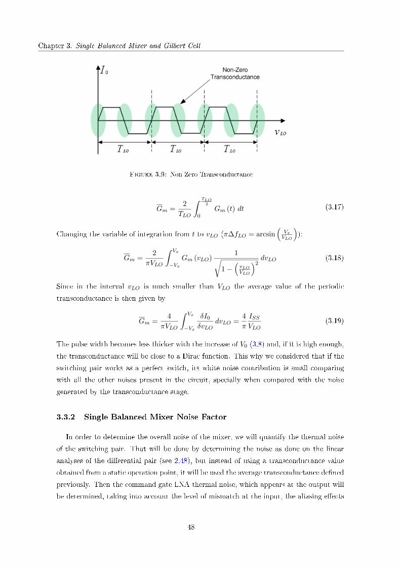
Chapter 3. Single Balanced Mixer and Gilbert Cell
Figure 3.9: Non-Zero Transconductance
Gm =2
TLO
∫ TLO2
0Gm (t) dt (3.17)
Changing the variable of integration from t to vLO (π∆fLO = arcsin(VxVLO
)):
Gm =2
πVLO
∫ Vx
−VxGm (vLO)
1√1−
(vLOVLO
)2 dvLO (3.18)
Since in the interval vLO is much smaller than VLO the average value of the periodic
transconductance is then given by
Gm =4
πVLO
∫ Vx
−Vx
δI0δvLO
dvLO =4
π
ISSVLO
(3.19)
The pulse width becomes less thicker with the increase of V0 (3.8) and, if it is high enough,
the transconductance will be close to a Dirac function. This why we considered that if the
switching pair works as a perfect switch, its white noise contribution is small comparing
with all the other noises present in the circuit, specially when compared with the noise
generated by the transconductance stage.
3.3.2 Single Balanced Mixer Noise Factor
In order to determine the overall noise of the mixer, we will quantify the thermal noise
of the switching pair. That will be done by determining the noise as done on the linear
analyses of the dierential pair (see 2.48), but instead of using a transconductance value
obtained from a static operation point, it will be used the average transconductance dened
previously. Then the command gate LNA thermal noise, which appears at the output will
be determined, taking into account the level of mismatch at the input, the aliasing eects
48

Chapter 3. Single Balanced Mixer and Gilbert Cell
associated with the oscillator harmonics (several harmonics will translate RF transconduc-
tance white noise to the IF output), and the conversion gain.
The thermal noise generated by the switching pair is:
V 2o nth,sw = 4KTγGm (RD)2
=16KTγ
π
ISSVLO
(RD)2
(3.20)
While the one generated by the Common Gate LNA, as seen in 2.34, is :
V 2o nth,cg = NV 2
nth,cg(Acα)2
α =1
[1 + (gmCG + gmbCG)RS ]
(3.21)
where N represents the power accumulated from all the oscillator harmonics which can be
determined applying the Parseval's identity. If we consider the square wave, the power
equivalence is
P =1
TLO
∫ −TLO2
−TLO2
|rect (t) |2 dt =∞∑−∞|Rn|2 =
∞∑1
8
π2(2n− 1)2(3.22)
This factor can be considered as a normalization factor, and it is equal to
N =π2
8(3.23)
Then the Common Gate thermal noise present at the output is
V 2o nth,cg =
π2
84KTγ(gmCG + gmbCG)
[2(gmCG + gmbCG)RD
π[1 + (gmCG + gmbCG)RS ]
]2
= 2KTγ(gmCG + gmbCG)
[RD
1 + (gmCG + gmbCG)RS
]2 (3.24)
It is important to clarify that since it is considered a conversion to the IF band the icker
noise it is not an issue (2.12), that is why only white noise was taken in account. Finally
49

Chapter 3. Single Balanced Mixer and Gilbert Cell
the thermal noises generated by the source and load resistances are
V 2o nth,RS = NV 2
nth,RS(Acα)2
=π2
84KTRS
[2(gmCG + gmbCG)RD
π[1 + (gmCG + gmbCG)RS ]
]2
= 2KTRS
[(gmCG + gmbCG)RD
1 + (gmCG + gmbCG)RS
]2
V 2o nth,RD = 8KTRD
(3.25)
Introduced all the noise sources, the total white noise at the output is
V 2o n,mixer = V 2
o nth,RS + V 2o nth,sw + V 2
o nth,cg + V 2o nth,RD (3.26)
The Noise Factor can be determined by (see equation 2.22):
NF =V 2o n,mixer
V 2nth,RS
(Acα)2=V 2o n,mixer
V 2o nth,RS
(3.27)
and that
V 2o nth,RS =
1
2KTRS
[1 + (gmCG + gmbCG)RS
(gmCG + gmbCG)RD
]2(3.28)
We have
NF = 1 +16KTγ
π
ISSVLO
(RD)21
2KTRS
[1 + (gmCG + gmbCG)RS
(gmCG + gmbCG)RD
]2
+ 8KTRD1
2KTRS
[1 + (gmCG + gmbCG)RS
(gmCG + gmbCG)RD
]2
+ 2KTγ(gmCG + gmbCG)
[RD
1 + (gmCG + gmbCG)RS
]2 1
2KTRS
[1 + (gmCG + gmbCG)RS
(gmCG + gmbCG)RD
]2(3.29)
50

Chapter 3. Single Balanced Mixer and Gilbert Cell
and
NF = 1 +8γ
πRS
ISSVLO
[1 + (gmCG + gmbCG)RS
gmCG + gmbCG
]2
+4
RSRD
[1 + (gmCG + gmbCG)RS
gmCG + gmbCG
]2
+γ
RS
1
gmCG + gmbCG
(3.30)
This derives in the following expression for the single balanced mixer Noise Factor:
NF = 1 +1
RS(gmCG + gmbCG)2
[(γ
8
π
ISSVLO
+4
RD
)[1 + (gmCG + gmbCG)RS ]2 + γ(gmCG + gmbCG)
]. (3.31)
This equation although simple does not allow trivial perception on which parameter in-
uences mostly the noise generated, as well as the rate of improvement allowed by the
variation of each parameter. However, by inspecting the equation we can conclude that if
the load impedance or the oscillator amplitude are increased the NF will be reduced (this
is interesting since both can be easily changed).
51

Chapter 3. Single Balanced Mixer and Gilbert Cell
3.4 MOSFET-Only Gilbert Cell Simulation
In this section we present a MOSFET-only implementation of a wideband Gilbert Cell
(3.10). The circuit uses a common-gate topology for a wideband input match, capable to
cover the WMTS frequency bands of 600 MHz and 1.4 GHz. In this circuit the load resistors
are replaced by transistors in triode mode, to reduce area and cost, and minimize the eects
of process and supply variations and mismatches. Therefore a comparison between the
conventional design with resistors, and the new MOSFET-only implementation in terms of
gain and NF will be made. Besides that the theoretical equations previously determined
for conversion gain and noise factor (4.20) as well as the conditions that ensures a switching
behavior will be validated.
The Gilbert Cell is based on two single balanced mixers (3.7), therefore both conversion
gain and noise factor expressions can be extrapolated. By looking at the circuit one can
see that each single balanced mixer will not produce the highest output at the same time,
so the dierential factor of two is not applied, hence the conversion gain of the Gilbert
Cell is equal to the single balanced mixer one. As far it concerns to the noise, apart from
the load impedance, the noise is twice the single balanced mixer noise. Both equations are
described in dB scale and are presented bellow.
Ac = 20 log
(2
π(gmCG + gmbCG)RD
)(3.32)
NF = 10 log
[1 +
2
RS(gmCG + gmbCG)2
[(γ
8
π
ISSVLO
+2
RD
)[1 + (gmCG + gmbCG)RS ]2 + γ(gmCG + gmbCG)
]]. (3.33)
52

Chapter 3. Single Balanced Mixer and Gilbert Cell
Figure 3.10: Wideband Gilbert Cell
The conversion from current to a voltage signal at the output of the mixer can be achieved
by a resistor load, RD, which has to be considered for both: conversion gain and noise
performance. An alternative approach is to replace these pure resistive loads by active ones
(3.11), based on PMOS devices, which are usually sized for saturation region. This has
the advantage of improving the overall gain, but the output DC common mode level might
have to be adjusted by means of additional circuitry, without aecting distortion (IIP3
and IIP2). Instead, this work explores the use of active loads operating in triode region
(2.6(b)), which simplies the overall process design, minimizing the distortion penalty.
Figure 3.11: Biasing Resistors Implemented With Active Loads
The design follows a transistor sizing approach that begins with the RF transconductance
stage, continues by sizing the mixing stage, and nally the active load is sized (3.12).
When compared with a pure resistive load, the PMOS active loads in triode region can
reach higher load AC resistance for the same DC biasing, thus improving conversion gain
and facilitating output voltage swing.
The complete design process involves:
53

Chapter 3. Single Balanced Mixer and Gilbert Cell
Figure 3.12: MOSFET-only Gilbert Cell Design Orientation
(a) Firstly, a low current source is selected in order to understate the power consumption;
(b) From the previous current, the CG RF transistor is sized in order to reach a transcon-
ductance level compatible with a 50 Ω input impedance matching. The transistor gate
biasing voltage is chosen such that the transistor is kept always in saturation region.
(c) Afterwards the transistors of the switching pairs, which perform the mixing operation,
are sized in order to be in saturation during the ON cycle while maintaining non-
conducting state during OFF cycle. Their sizes also have to ensure a low impedance
node between the RF and mixing stage while at the output IF node their output
resistance shall be much higher than the active loads. In order words, gds,sw << gds,D,
andgm,sw
2 << gds,cg;
(d) To ensure that a strong and well dened switching operation at the mixing stage, the
VLO is selected to be larger than√
2Vdsatsw . However, additional headroom has to be
taken into account to accommodate second order parasitic eects.
(e) Finally, the PMOS active loads are sized. The optimization is reached, by putting
them in triode region, but suciently close to saturation (to improve small signal
resistance). The nal widths are then ne tuned in order to obtain sharper switching
current transitions (the slopes are aected by the circuit parameters, 3.13).
54

Chapter 3. Single Balanced Mixer and Gilbert Cell
Figure 3.13: Switching Pair Current Characteristic Degeneration
(f) The length used for each transistor was the maximum value allowed by the technology,
this is intended to help preventing process variations.
(g) This circuit is not intended for implementation, therefore, no special concern is taken
in account to ensure enough voltage headroom for current mirrors.
The design obtained is as follows.
Figure 3.14: MOSFET-only Gilbert Cell Design Values
55

Chapter 3. Single Balanced Mixer and Gilbert Cell
To validate the theoretical equations (3.34 and ??), rst the circuit is simulated with
resistors (the resistance value is selected in order to maintain the same DC point) with a
value of 433 Ω. The simulations were made with Cadence Spectre RF using BSIM3v3 for
a 130 nm MOS technology. RF frequencies of 600 MHz and 1400 MHz were considered.
The amplitude of the RF input signal is set to 2 mV. This circuit has a power consumption
of only 3.6 mW drawn from a 1.2 V power supply. Under these design values, a theoreti-
cal voltage conversion gain of 14.65 dB, and a noise factor of 9.1 dB are estimated. The
simulations results were the following:
Table 3.1: Gilbert Cell Conversion Gain And Noise Factor Using Resistive Loads.
Gilbert Cell w/ res.600 MHz 1400 MHz
IF (MHz) Ac (dB) NF (dB) Ac (dB) NF (dB)
20 14.27 9.6 12.5 10.440 14.25 9.6 12.5 10.460 14.16 9.6 12.5 10.480 14.16 9.6 12.5 10.3100 14.07 9.6 12.5 10.3
The simulations results of 3.1 show that the approximations used results on a maximum
error of 15% for the conversion gain and a maximum error of 12.5% for the NF over the
WMTS band. The results show also a degradation as the frequency of the carrier increased,
this is a result expected due to the parasitic eects.
Afterwards the circuit is simulated with the active loads in triode region. A MOS transistor
operating in triode region can be modeled by a resistor only if gds/gm > 10, otherwise the
transistor should be modeled by a resistance in parallel with a current source. In this case
we can increase the incremental load resistance without increasing the DC voltage drop.
This allows the gain to be increased with respect to the circuit with "true" resistors [14, 15].
The saturation region is reached when gm is of about the same magnitude as gds.
Thus, the equations previously determined for the Gilbert Cell must be now adapted to
include the active load equivalent impedance (assuming the transistor are in triode region).
The new equations are:
Ac = 20 log
(2
π
(gmCG + gmbCG)
gds,D
), If (gmCG + gmbCG) << gds,D (3.34)
56

Chapter 3. Single Balanced Mixer and Gilbert Cell
NF = 10 log
[1 +
2
RS(gmCG + gmbCG)2
[(γ
8
π
ISSVLO
+ 2gds,d
)[1 + (gmCG + gmbCG)RS ]2 + γ(gmCG + gmbCG)
]]. (3.35)
For the circuit with active loads a theoretical conversion gain of 22.3 dB, and a noise
factor of 8.4 dB are estimated. The simulation results show a maximum conversion gain of
20.3 dB and a maximum NF of 10.5 dB as seen in Fig. 3.15.
(a) (b)
Figure 3.15: (a) Conversion Gain (Ac) curve (b) Noise Factor (NF ) curve
Figure 3.16: Simulated Conversion Gain (Ac) and NF (NF )as a Function Of the Load Tran-sistor Width. IF = 20 MHz, LO = 580 MHz, RF = 600 MHz
57

Chapter 3. Single Balanced Mixer and Gilbert Cell
As shown in Fig. 3.16, in order to maintain the transconductance and switching stages
under saturation, the size of the triode load has a limited range (as it enters in region
A the output impedance becomes so large that the saturation, is not achievable in all
transistors and the gain begins to collapse). Maximizing gain, means to choose a load
transistor width close to the optimal point, shown in Fig. 3.16. Finally, in Tab. 3.2 a
comparison is made between the simulated results obtained for the mixer when using pure
resistive load and alternative triode ones.
Table 3.2: Active Load versus Resistive Load over the 600 MHz band.
G. Cell w/ MOS. (1048 Ω) G. Cell w/ Res. (433 Ω)IF (MHz) Ac (dB) NF (dB) Ac (dB) NF (dB)
20 20.33 9.5 14.27 9.6100 20.05 9.4 14.07 9.6
The DC voltage drops between the two cases are maintained. As expected, an improvement
of the conversion gain is obtained with similar NF level. The eect of the icker noise is
reduced since the used IF frequency is suciently away from the 1/f corner frequency.
Finally, the IIP3 of both implementations is simulated for comparison (see Fig. 3.17(a)
and Fig. 3.17(b)). The implementation with resistors presented an IIP3 value of -6.06
dBm and a IIP3 value of -8.22 dBm for the implementation with active loads. As we can
conclude did not have signicant impact of the mixer linearity.
58

Chapter 3. Single Balanced Mixer and Gilbert Cell
(a)
(b)
Figure 3.17: (a) Gilbert Cell IIP3 With Resistors (b) Gilbert Cell IIP3 With Active Loads
As a nal observation, if we consider the optimal design point, where the Signal to Noise
ratio is improved, we can see that the switching pair current commutation characteris-
tic is not well behaved as shown in Fig. 3.18, and yet good performance and accurate
approximations were achieved.
Figure 3.18: Switching Pair Current Characteristic in the Optimal Point
59

Chapter 3. Single Balanced Mixer and Gilbert Cell
By hypothesis, if we relax the current characteristic (meaning that the current gain is no
longer 2π , due to slower transitions) and at the same time ensure that,
2
πsinc(∆πfLO)(gmCG + gmbCG) <<
1
gds,D(3.36)
the circuit is likely to be optimized without aecting signicantly both conversion gain and
NF. Under those conditions, comparable performance can be obtained with reduction of
the LO power and/or reduction of the switching pair width (the idea is to generate only
enough distortion on the switching pair in such a way that an IF signal is produced).
Discussion
In this section a MOSFET-only implementation of a Gilbert Cell was presented, based
in a CG wideband input match. In MOSFET-only circuits, the replacement of resistors
by transistors reduces the area and cost and minimizes the eect of process and supply
variation and of mismatches. Besides that this new approach proposed adds a new degree
of freedom, which can be used to optimize the mixer gain: we can obtain a higher gain
than with resistors for the same DC voltage drop, with a minimum impact on the NF.
It was also demonstrated that despite the rough approximations made, such as neglecting
parasitics, output conductances and distortion generation mechanisms, the equations used
for both conversion gain and noise factor were accurate.
60

Chapter 4
Two Integrator Oscillator
4.1 Introduction
Oscillators have wide applications in instrumentation and communication systems. In
particular they are key blocks in modern RF front-end architectures. So it is very impor-
tant to have a reliable and ecient wave generator with stable frequency and phase (the
outputs must be precise because any deviation will compromise the SNR).
In this chapter a linear tunable oscillator using CMOS technology, the Two Integrator os-
cillator (see Fig. 4.1), will be presented and discussed [16, 17, 18]. It has inherent good
quadrature outputs, the working frequency can be tuned over a wide range and although
it has lower quality factor comparing to a LC oscillator, it has similar phase noise perfor-
mance. It also requires a much smaller area which obviously is reected in overall cost and
integration.
61

Chapter 4. Two Integrator Oscillator
Figure 4.1: CMOS Two-Integrator Oscillator
Basically the two integrator oscillator is constituted by two stages, with cross coupled
connection, each one with an integration block (see Fig. 4.1 lower region) formed by a
dierential pair that acts as a current buer and a capacitor, which represents the parasitic
capacitances connected to the dierential pair output nodes. Since the parasitic capaci-
tances of the transistors used act like an integrator (4.2), there is no need for using a real
capacitor in the feedback network, thus reducing the circuit area. There is also another
dierential pair (see Fig. 4.1 upper region) with cross-coupled outputs used for loss com-
pensation and amplitude stabilization.
62

Chapter 4. Two Integrator Oscillator
Figure 4.2: Equivalent Circuit Capacitance
The upper dierential pair acts also as a controller. It controls in which direction the
capacitor is charged, and the wave form current that is fed to the integrator as shown in
Fig. 4.3(a),4.3(b).
(a) (b)
Figure 4.3: (a) Phase 1 (b) Phase 2.
For better understanding, this study will be focused in explaining how the outputs are gen-
erated, by detailing how it complies the Barkhausen Criterion conditions, and the behaviors
which lead to two dierent output waves. The exhaustive explanation of an oscillator is
complex, therefore this study is more suitable to a qualitative description by using simple
models and equations. This approach will also provide some simple design guidelines.
63

Chapter 4. Two Integrator Oscillator
4.2 Barkhausen Criterion
First the Barkhausen Criterion will be seen from another standpoint. If one consider
the following functions:
x1(t) = cos (ω0t) (t ≥ 0)
x2(t) = sin (ω0t) (t ≥ 0)(4.1)
They have respectively the following Laplace's Transform:
X1(s) =s
s2 + ω20
X2(s) =ω20
s2 + ω20
(4.2)
The poles are determined by equaling the denominator to zero:
s2 + ω20 = 0
s2 = ±jω0
(4.3)
This means that the ideal oscillator is a system with imaginary conjugated poles.
Figure 4.4: Steady State Oscillations
4.2.1 Phase Condition
Usually a simple oscillator is done with a resonant circuit, that is made with a capacitor
connected in parallel with an inductor. Since each device produces a phase shift of 90, the
result is a system with a pure imaginary conjugate poles. However, in this oscillator there
are no passive inductors, and at a high level the oscillator can be seen as two integrators
and an inverter in a feedback loop. The two integrator capacitors add each one a phase
shift of -90 (derived from the capacitor's impedance equation ( 1jωC ) and the cross wired
64

Chapter 4. Two Integrator Oscillator
connection between the two stages, that causes a signal inversion, produces an extra phase
shift of -180.
However, if one look at the following,
1
jωC(−1) =
1
jωC(j)2 = j(ωC)−1 (4.4)
one can understand that, despite the fact that no actual inductors were used, a structure
with two poles is obtained since the equivalent phase shift of a passive inductor is emulated
by the capacitor and the cross-connection. To analyze the circuit, to see if it complies the
phase condition, one must pay attention that this circuit is formed by two smaller struc-
tures with two types of feedback, a positive feedback (direct coupling, 4.5), and a negative
feedback (cross coupling, 4.6).
Figure 4.5: Direct Coupling in the Two-Integrator Oscillator
65

Chapter 4. Two Integrator Oscillator
Figure 4.6: Cross Coupling in the Two-Integrator Oscillator
This oscillator can be seen as a having a positive feedback and since it has an overall
network phase shift of 360 it complies the Barkhausen criterion phase condition (see equa-
tion 2.54).
4.2.2 Gain Condition
As seen in Fig. 4.4, to achieve stable oscillations (amplitude stabilization), pure imag-
inary conjugate poles must exist, which means that the real part of the poles must be
eliminated. The real part appears due to resistive elements, and since resistors are used
for biasing the circuit it would be expected that the circuit could not maintain stable os-
cillations. However, as referred before, apart from the integration block there is in each
stage an additional dierential pair (transistors MB), with the output cross-coupled to the
inputs as shown in Fig. 4.7) which are responsible for moving the poles over the imaginary
axis [19].
66

Chapter 4. Two Integrator Oscillator
Figure 4.7: Cross-Coupled Dierential Pair
As it can be seen in the small signal analysis (4.8), by cross coupling the dierential pair
outputs, an equivalent negative resistance (4.5) is obtained.
↓ ↓
2xv
2xv
2
gmvx
2
gmvx
xi
xv
Figure 4.8: Small Signal Analysis of Cross-Coupled Dierential Pair
rx =vxix
= − 1
gm(4.5)
If the dierential pair is designed and biased in such a way that,
gm =1
RD(4.6)
the losses due to the biasing resistors are compensated (only the resistors are contemplated
as losses since the transistors are in saturation region, which means that they present very
high output impedances compared to R) and the result is the elimination of the real part
67

Chapter 4. Two Integrator Oscillator
of the poles. The practical result is that the lower dierential pair will have no voltage
gain, therefore an ideal integrator is obtained and the gain condition of the Barkhausen
criterion gain is found.
However, for start-up, the circuit needs to be unbalanced, which is accomplished by over-
compensating the losses (4.9). In practice this means that the lower dierential pair will
exhibit a voltage gain, in addition to the noise present in the circuit it will allow the circuit
to get out of the DC point:
gm >1
RD(4.7)
Figure 4.9: Amplitude Stabilization
One important aspect is that this cross-coupled pair has a similar behavior as the dierential
pair in the single balanced mixer described in chapter 3, which means it also has a varying
transconductance (Figure 4.10).
68

Chapter 4. Two Integrator Oscillator
Figure 4.10: Transistor Variable Transconductance and Dierential Pair Periodic Transcon-ductance
This is in fact a feedback circuit which means that the average transconductance will
converge to the point where it compensates the losses (this is another reason why the
losses at startup must be overcompensated, 4.9). Since the equivalent dierential pair
transconductance swings, the consequence is that the poles are not kept constantly over
the imaginary axis, thus, resulting in phase noise since in reality it is impossible to obtain
a constant frequency at the output. The study of phase noise based on poles variation is
quite complicated and is out of the scope of this thesis [11].
4.3 Linear Model and Carrier Characterization
At this point one knows that since the lower dierential pair,Mf has no voltage gain (in
average) it acts only as a merely transconductance stage (current buer), and the upper
dierential pair, MB acts as a negative resistor. This allows to do a simple circuit char-
acterization by using a linear model, thus retrieving both amplitude and frequency of the
generated carrier signal.
Figure 4.11: Linear Model of the Two-Integrator Oscillator
69

Chapter 4. Two Integrator Oscillator
Since the Ituning current is integrated by the capacitor, the voltage output will be mainly
dened by the current Ilevel and the load resistors. Therefore the amplitude of the produced
carrier signal can be easily obtained:Vmax = Vdd − (Vdd −RDIlevel)
Vmin = Vdd − (RDIlevel − Vdd)(4.8)
VLO = RIlevel (4.9)
This model also has the following loop gain
|H(jω)| =g2mfω2C2
p
(4.10)
Since the gain must be one for oscillations (see equation 2.53),
|H(jω)| =g2mfω2C2
p
= 1 (4.11)
The output frequency can be obtained
ω =gmfCp
(4.12)
This is why this oscillator is said to have a wide tunning range, since with a simple
manipulation of the Ituning current value, the transconductance gmf can be changed thus,
allowing to sweep a large range of frequencies.
4.4 Two Integrator Oscillator Behaviors
This oscillator is capable of producing two types of output. Basically since the upper
dierential pair acts as amplitude limiter (the lower dierential pair has no voltage gain
and it only aects how fast or how slow the biasing point of the commutation pair variates.
See equation 4.8) it controls the shape of the signal that is fed to the integration block.
Since the lower dierential pair is designed to work in the linear zone, it will just produce
a current signal with the same physical properties of the input signal (the one generated
by the commutation pair), therefore the output waveform will be mainly dependent on the
operation point of the commutation pair (4.12, where vLO is the amplitude of the carrier
signal produced as in 4.9).
70

Chapter 4. Two Integrator Oscillator
Figure 4.12: Currents Produced by the Dierential Pair and Regions of Operation
This means that we can distinguish two behaviors in this oscillator, a Linear behavior and
a Non-Linear behavior according to the operation region of the commutating pair.
4.4.1 Linear Behavior
This behavior is obtained by designing the commutation pair to work in the linear zone
(Fig. 4.12, this region is dened over small variations of input voltage around the DC
point). Since the dierential pair acts as a current buer, the maximum current produced
at the output is ILevel, therefore, the amplitude of the carrier signal generated is given by
4.9. According to the study of the dierential pair the condition that ensures this behavior
is then:
vLO <√
2VdsatMb (4.13)
By ensuring this behavior, a new linear model can be considered for the oscillator. Since
both dierential pairs are working on the linear zone, it is possible to replace the commu-
tation pair by a soft-limiter as shown in 4.13. In this way the circuit is assumed as being
linear with an output amplitude lower than the soft-limiter levels (4.14).
1
1 1 2 2
Figure 4.13: High Level Model in Linear Behavior
71

Chapter 4. Two Integrator Oscillator
Figure 4.14: Two-Integrator Output Waveform in Linear Behavior
As one can see, the result is the generation of sine-waves as carrier signals. This behavior
condition is:
RDILevel <√
2VdsatMb (4.14)
4.4.2 Non-Linear Behavior
This behavior is obtained by designing the commutating pair to work in the non-linear
zone (Fig. 4.12). This provides a behavior similar to the one seen in the single balanced
mixer, which means that the commutation pair will have a square-wave current charac-
teristic, thus achieving a switching behavior. The condition that ensures this behavior is
then
vLO >>√
2VdsatMb (4.15)
However, in this operation mode the dierential pair no longer acts as ideal current buer
due to the distortion caused by the non-linearities; then a new approximation for the
amplitude of the carrier must be considered. From the study of the single balanced mixer,
one knows that a dierential pair working as a switching pair shows a well known average
transconductance as shown in equation 3.19.
Gm =4
π
ILevelVLO
(4.16)
and from the theory of the oscillators we know that if the amplitude condition required
for steady state oscillations is found the average transconductance compensates the circuit
losses:
Gm =1
RD(4.17)
72

Chapter 4. Two Integrator Oscillator
which means that a new equation for the oscillator signal magnitude can be derived
vLO =4
πRDILevel (4.18)
The behavior condition becomes:
4
πRDILevel ≥
√2V dsatMb
(4.19)
By doing a similar procedure as made for the linear behavior, this switching pair can be
modeled as a Schmitt Trigger (4.15). The model obtained is the following:
1
1 1 2 2
Figure 4.15: High Level Model in Non-Linear Behavior
Figure 4.16: Two-Integrator Output Waveform in A Non-Linear Behavior
Since a square wave is fed to the integrator, the result is a triangular-wave as carrier signal
(the non-linearities introduced by the switching pair resulted in an output signal with
several odd order harmonics Fig. 4.16).
73

Chapter 4. Two Integrator Oscillator
4.4.3 Simulation and Discussion
As it was referred at the beginning of this thesis, the Two-Integrator oscillator under a
non-linear behavior is the starting point for implementing the combined structure. There-
fore, the conditions that ensure this behavior as well as the approximation derived of the
oscillator amplitude working in this regime will be tested (equations 4.19 and 4.18). This
will also help to identify if a switching pair is in fact obtained, since at plain sight is di-
cult to identify a fairly good square wave current characteristic. It will be considered and
discussed the MOSFET-only implementation of the Two Integrator Oscillator (4.17).
Figure 4.17: MOSFET-only Two-Integrator
The design should comply three conditions:
(a) The losses at startup must be overcompensated, therefore gm) > gds,D.
(b) To facilitate the acquisition of the switching behavior the upper dierential pair
should have transistors with low Vdsat value.
(c) The lower dierential pair should work in the linear region of the dierential pair
characteristic to reduce the distortion and introduced non-linearities.
74

Chapter 4. Two Integrator Oscillator
The last two conditions can be described as following (assuming a switching behavior of
the upper dierential pair):
√2VdsatMf >
4
πRDILevel
Since the lower dierential pair is aected by the same oscillator signal:
√2VdsatMB <<
4
πRDILevel
(4.20)
which means that
V dsatMf>> V dsatMB
(4.21)
and, nally (W
L
)Mf
<<
(W
L
)MB
(4.22)
If we ensure a high ratio between both dierential pair sizes, we can manipulate the transi-
tion of the oscillator behavior by simple variation of the load impedance, while the lower dif-
ferential keeps a linear behavior. The simulations will consist in varying the load impedance
and the Ituning current together to maintain the oscillator tuned for the 600 MHz band.
Therefore we will start with a small impedance of 125 Ω, ensuring the oscillators linear
behavior, and gradually increase it until a maximum value of 300 Ω. In between the oscil-
lator should transit from the linear behavior to the non-linear one. The circuit is designed
as follows:
Figure 4.18: Two-Integrator Design Values.
75

Chapter 4. Two Integrator Oscillator
The simulation results obtained can be seen below (4.19). It are also shown the obtained
current characteristics of both dierential pairs (Fig. 4.20(a), 4.20(b)), when the load
impedance, RD, is respectively 125Ω and 300Ω.
Figure 4.19: MOSFET-only Two-Integrator Parameters and Simulation Results
(a) (b)
Figure 4.20: (a) Dierential Pairs Current Characteristics with RD = 125 Ω (b)Dierential Pairs Current Characteristics with RD = 300 Ω
The oscillator transits from the linear behavior to the non-linear behavior. In between
there is a transition zone, where the commutation pair presents neither a sine wave neither
a square wave. As it enters the non-linear behavior we can see that the equation dened for
this behavior is really accurate. As the non-linearities increase and the upper dierential
pair becomes a switch, the eective current produced, I0Level, is larger than the one fed by
the DC current source ILevel, which justies the increase of the supposed carrier magnitude.
I0Level ≈4
πILevel (4.23)
It is also possible to observe that the eective I0tuning never reaches the value of the
DC current source, due to two major reasons, the rst one is that since its working in the
linear region it never cuts o. The other reason is in respect to the switching pair that acts
as amplitude limiter an it does not allow this pair to reach the maximum current.
76

Chapter 4. Two Integrator Oscillator
It is important to see that the current characteristic, where the theoretical oscillator mag-
nitude equation for the non-linear behavior meets exactly the simulated result (see Fig.
4.21), is a fairly good square wave.
Figure 4.21: Current Characteristics When VLOteo = VLOsim
This means that by comparing the theoretical expression with the simulated one a good
switching characteristic can be identied (if the values match the average transconductance
of a square wave is the intended), which means excessive oversizing of the switching pair
can be avoided as well as distortion which allows optimization process.
It is important to underline that this simulations were done on a tuned circuit on the 600
MHz band. If it is needed to cover a larger band as for instance, the three WMTS bands,
the desired behavior of each dierential pair should be expected to be dicult to maintain
over the working band (specially due to parasitics) and a few design compromises must be
made.
77


Chapter 5
LOM Design and Simulation
5.1 Introduction
The Two Integrator Oscillator generates two I/Q signals with the upper dierential act-
ing as a switching pair. If a low power high frequency current signal is fed to the switching
pair common source (iRF ), a single balanced mixer structure is obtained as shown in Fig.
5.1, and an IF signal can be produced at the output of the circuit (thus, the circuit would
be able to present conversion gain). It is considered that the low power input signal should
not aect the functioning of the dierential pair, specially its ability to compensate the
losses and still obtaining steady state oscillations.
79

Chapter 5. LOM Design and Simulation
Figure 5.1: Single Balanced Mixer Structure in the Two Integrator Oscillator
Considering instead of an ideal current source ILevel a LNA to provide the input current
(ILevel+iRF ) with low current gain and with the ability of achieving 50 Ω input impedance
matching a remarkable small RF front-end is obtained, the LOM. With this merged topol-
ogy, there is a reduction of the biasing elements (the DC consumption can be better sized),
the current is reused and does not required the use of matching buers. This results in a
strong reduction of the number of transistors used comparing with the number that nor-
mally would be used in designing these three blocks separately. The LOM will be also
designed with active loads instead of common biasing resistors, which results in a low
power, low cost and low area MOSFET-only RF front end which meets the main require-
ments for WMTS biomedical applications. Under this assumption this particular circuit
will be intended to cover the frequency range of WMTS bands and it will be designed with
the main goal of understating power consumption and area, with no special regards about
conversion gain, noise or linearity optimization.
In this chapter the LOM will be presented and simulated. Some considerations will be
made concerning the design procedure, behavior, validity of theoretical equations and de-
gree of application of this circuit. Although noise generation and distortion mechanism are
not fully predictable and understandable it will be shown that a simple qualitative and
straightforward design methodology will still oers a good approach with wide range of
validity.
80

Chapter 5. LOM Design and Simulation
5.2 Low Noise Amplier Validation And Discussion
In this section conventional LNA topologies will be evaluated in order to select the best
one to be integrated in the Two Integrator Oscillator. It will be selected taking in account
its occupied area, noise produced, input impedance matching characteristics, and the most
important, it should work with low voltage supply (it is expected the nal circuit to have
low voltage headroom, therefore, cascade topologies will not be studied).
In chapter 3 a Common Gate Stage was used to implement the LNA, due to its easy
gain and noise description and quantication. It has also the advantage of allowing the
implementation of a wideband circuit, since its does not require a tuned input matching.
However, due to its resistive input impedance, it presents a high NF when compared with
other topologies. The idea behind this section is to test if there is a more balanced and
suitable topology for integration. The tested circuits are exposed below.
Common Source LNA
As referred in chapter 2 the common source stage is used to implement a dierential
pair. However this stage is often used as amplier to implement LNA's. The resistive
input match can be made by placing a resistor in parallel with the amplier input (5.2(a)).
However, this has a major problem, the use of an additional resistor increases the overall
noise factor (it becomes greater than the one generated by a CG stage). However, this
type of matching does not allow a perfect match, since the input impedance of a common
source is typically capacitive, thus, requiring the use of reactive components for maximum
power transfer (5.2(b)). This results in two important issues, rst this results in a tuned
narrow band LNA (it should work only at a given frequency), which is not intended (the
LC network denes a band pass lter). Besides that, considering a full on-chip integration,
inductors occupies a large area increasing signicantly the chip cost (its size is comparable
with a full RC oscillator).
81

Chapter 5. LOM Design and Simulation
(a) (b)
Figure 5.2: (a) Common-Source Stage with Resistive Match (b) Common-Source Stage withInductive Match and Source Inductive Degeneration
Wideband Balun LNA
Afterwards it is considered a wideband Balun LNA (5.3). This circuit is able to provide
resistive impedance matching, and partially noise cancellation resulting in a low NF when
comparing with a CG stage [15, 20]. This is an obviously protable topology since the
circuit where is supposed to be integrated already has several noise sources.
Figure 5.3: Balun LNA
The principle of operation is the following; the noise signal generated by the CG stage is
inverted by the CS stage, and then if a dierential output is retrieved the noise of the CG
is partially canceled. However, for this to work both signals must be in phase, and the
amount of noise cancellation depends on the mismatch of both stages gain.
Therefore, it was considered ways to connect this circuit to the oscillator, which are dis-
cussed below.
82

Chapter 5. LOM Design and Simulation
(a) (b)
(c)
Figure 5.4: (a) Blixer Structure (b) Connection Based On Gilbert Cell (c) Shunt Blixer
83

Chapter 5. LOM Design and Simulation
(a) In the rst case (5.4(a)), we can clearly see that in this situation, although the
properties of the Balun are kept, the full circuit would behave as gain block, since
the dierential pair no longer exists. Without this dierential pair, oscillations are
not produced neither is the mixing function. In fact what is obtained is a cascode
type structure[21].
(b) The second case is dierent (5.4(b)), although the circuit could oscillate and maintain
the mixing function, there is no way to combine the outputs to produce quadrature
output signals along with noise cancellation (due to phase dierences). This has
another problem, since it may be dicult to generate exactly the same current to
feed both switching pairs, which can result in output signals with dierent amplitudes.
(c) The nal case presuppose that instead of voltage cancellation, a current cancellation
can be done by short-circuiting the outputs of the Balun (5.4(c)). This would result
in canceling the noise before fed it to the switching pair. What would seem like the
perfect solution is not, since the outputs of both branches of the balun are in-phase
(in theory) doing this would double (rough consideration) the noise while the signal
of interest would be wiped o. This does not happen exactly since perfect match
between both transistors is dicult to achieve.
In an attempt to correct this last implementation an update to the balun is considered.
The dierential eect could be emulated by inserting another CS stage (the noise produced
by the CG would be inverted twice). This would allow the noise to be canceled in current
domain (5.5).
84

Chapter 5. LOM Design and Simulation
Figure 5.5: Noise Cancellation in Current Domain
As one can see the number of noise sources increased and, if we consider the CMOS im-
plementation, so it did the total area. This would not be such an issue if the circuit would
work as expected. Some simple simulations showed that, due to parasitics, the noise that
ows trough the CS branch is delayed, which means that the noise cancellation is not done
correctly. The parasitic eects can be diluted by using high currents to bias the second CS
stage, since this work is intended to understate the power consumption this is not a suit-
able solution. The hypothesis is to design in lower scale technology (less parasitic eects),
which can be interesting for further studies. Since the noise cancellation cannot be done
this circuit is discarded.
In conclusion the best suitable topology, taking in account the design restrictions, is the
Common Gate stage. It will allow an implementation of a wideband LNA in the smallest
possible area.
85

Chapter 5. LOM Design and Simulation
5.3 Combined LNA-Oscillator-Mixer
At this point is possible to resume the previously dened circuit conditions and proceed
to nal design:
All transistors (except loads which operate in the triode region)must be sized in order
to remain in saturation all the time when active (switching pair case).
Transistors should have at least a Vdsat of 100 mV for proper biasing (due to the
current levels, moderate inversion should be achieved). It should be used also the
maximum length allowed over 3Lmin in order to understate process variations.
The design must secure voltage headroom for current sources implementation using
simple current mirrors.
Since the input RF signal will be fed simultaneous to both stages the individual
transconductance of each CG should be 10 mS instead of 20 mS. This means each
CG RF transistor is sized in order to reach a transconductance level compatible with
a 100 Ω input impedance matching. This particularity allows a reduction of the
transistors size and bias current, Ilevel.
The sizing of all transistors must consider node impedance independence:
gm,sw2 << gds,cg
gds,sw << gds,D
gds,f << gds,D
The losses at startup must be overcompensated, therefore gm,sw > gds,D.
A down-conversion of the input signal can be done by using carriers with higher or
lower frequency than the RF frequency. However since higher frequency means higher
Ituning current, it should be use lower LO frequencies to do the down-conversion.
Therefore the design should be aimed to produce a maximum LO frequency of 1.3
GHz.
The upper dierential pair should work as a switch to ensure the mixing function
and the lower dierential pair should work as a gain block (linear characteristic).
Therefore:√
2VdsatMf >4πRDILevel
√2VdsatMsw <<
4πRDILevel(
WL
)Mf
<<(WL
)Msw
86

Chapter 5. LOM Design and Simulation
Design Constraints:
It will be reserved a safety voltage margin of 100/150 mV for current mirrors imple-
mentation.
Since the circuit is supposed to have low area none of the transistors used should
exceed a multiplier of one (Wmax = 115.2µm).
The CG bias voltage will be set to a common reference voltage of 600 mV.
The 1.4 GHz carrier should be produced with a Ituning current below 2.5 mA.
Design Methodology:
(a) First, a low output impedance of 150 Ω was selected, alongside with a ILevel current
of 1mA and a Ituning current of 1.5 mA (no specic LO frequency is tuned).
(b) As referred in the Two-Integrator non-linear behavior study, the size of this pair could
be optimized. But that should only be possible if the circuit could present similar
behavior throughout the whole working band (see Fig. 4.21. Therefore since this
condition is not veried the maximum allowed size is selected for the switching pair.
(c) The size of the lower dierential pair is selected as the minimum size that does not
compromise the shape of the current characteristic (if it is to small the wave begins
to distort).
(d) Afterwards the CG is sized to ensure input impedance matching and low output
conductance.
(e) Since its dicult to maintain optimal circuit behavior over the WMTS band (a switch-
ing pair and a gain block), the PMOS active loads were increased until the 1.4 GHz
LO frequency is achieved with an Ituning current of 2.5 mA. Better circuit behavior
should be achieved with higher current however this designs aims for power consump-
tion reduction. The load value should be such that ensures saturation region for all
transistors and enough voltage headroom for current mirror implementation.
(f) Afterwards the load value is determined the size of the CG is adjusted.
87

Chapter 5. LOM Design and Simulation
The design obtained is the following:
Figure 5.6: LOM Design Values
The DC parameters (5.1,5.1) and current characteristics (5.7(a), 5.7(b)) obtained can be
seen below.
Table 5.1: Circuit Parameters with fRF = 600 MHz
fIF fLO Ituning gds,D1
gds,Dgmcg gmbcg gmsw,DC
(MHz) (MHz) (µA) (mS) (Ω) (mS) (mS) (mS)
20 580 673.5 5.18 193 9.07 1.03 9.0240 560 648 5.2 192 9.07 1.03 9.0260 540 623.5 5.22 192 9.08 1.03 9.0280 520 599.5 5.23 191 9.08 1.03 9.02100 500 571 5.25 190 9.08 1.03 9.02
Table 5.2: Circuit Parameters with fRF = 1400 MHz
fIF fLO Ituning gds,D1
gds,Dgmcg gmbcg gmsw,DC
(MHz) (MHz) (µA) (mS) (Ω) (mS) (mS) (mS)
20 1380 2.44 3.7 270 8.7 1 940 1360 2.34 3.8 263 8.8 1 960 1340 2.254 3.89 257 8.8 1 980 1320 2.18 3.95 253 8.8 1 9100 1300 2.09 4.04 248 8.82 1.01 9
88

Chapter 5. LOM Design and Simulation
(a) (b)
Figure 5.7: (a) fLO = 500 MHz (b) fLO = 1300 MHz
As we can see the desired behaviors are not kept throughout the whole working band.
Since a maximum value of tune current is selected, the lower dierential pair at the min-
imum working frequency presents distortion. This is due to the low current required for
tuning this frequency, which derives in a low Vdsat value therefore this makes the dierential
pair easily subject of the high carrier magnitude.
89

Chapter 5. LOM Design and Simulation
LOM Periodic Steady State Simulation
Since this is a combined circuit that generates itself its own oscillator signal, it is im-
possible for the simulator to determine the fundamental frequency it should be using hence
it is impossible for the PSS analysis to converge to a solution. To override this problem
auxiliary dummy sources were connected to the circuit (5.8). This sources have zero ampli-
tude however they should have phase shifts dened or else the circuit will present voltage
dierences on its branches. With this sources no longer an initial condition is required for
the circuit to begin oscillations since they produce enough noise for the system to startup.
Figure 5.8: Dummy Sources
Simulation Process:
(a) First, an input frequency signal is injected.
(b) Next the IF desired frequency is stipulated and the required LO frequency is deter-
mined.
(c) The LO frequency value is then placed on each dummy source.
(d) Afterwards the circuit is tunned for this LO frequency by varying the Ituning current
and conrmed by a transient analysis.
(e) Next the PSS and Pnoise are analysis are made.
Since the lower dierential pair is assumed to have no voltage gain, an independence
between both stages, at the band of interest, should prevail. Which means the eective IF
90

Chapter 5. LOM Design and Simulation
amplitude generated should be the one generated by the single balanced mixer. Besides,
it was considered that the system should work properly when the switching pair, MSW
presents a non-linear behavior and the lower dierential pair, Mf , presents a linear be-
havior. Since the circuit is not able to maintain these behaviors as the Ituning current is
increased, rst we tried to nd the frequency range where the desired behavior should be
achieved to do some considerations.
By visual inspection the ideal behavior was found when the circuit is tuned to a LO fre-
quency between 1100 MHz and 1200 MHz as shown in Fig. 5.9(a) and Fig. 5.9(b).
(a) (b)
Figure 5.9: (a) fLO = 1100 MHz (b) fLO = 1200 MHz
As one can see the waveforms at plain sight seems to be the desirable ones, conrma-
tion should however be done through simulation, which was done considering (The results
obtained are shown in Tab. 5.3):
VLONL =4
πRDILevel
Ac = 20 log
(2
π
(gmCG + gmbCG)
gds,D
) (5.1)
Table 5.3: LOM, Under Optimal Behavior, Parameters and Simulation Results
fRF fIF1
gds,DVLONL VLOsim Ac Acsim
(MHz) (MHz) (Ω) (mV) (mV) (dB) (dB)
1200 100 222 283 289 2.9 3.21300 100 233 296 308 3.3 2.6
The estimated carrier amplitude almost meets the simulated one as well as the conversion
gain that presents low error of approximation, however this could be due to the frequency
degeneration (the circuit has the inherent frequency response of the oscillator, which is, as
we know, a band pass lter response) at it may be a coincidence. Further study should be
91

Chapter 5. LOM Design and Simulation
done to dispel the doubts about this approach.
Afterwards the circuit was simulated to see if these observations are seen throughout the
entire working frequency range. The simulation results are shown in Tab. 5.4 and were
done considering the following (it will be taken in account, as reference, the Noise Factor
estimation for a single balanced mixer):
Rin =1
2(gmCG + gmbCG)
VLOL =ILevelgds,D
NF = 10 log
[1 +
1
RS(gmCG + gmbCG)2
[(γ8
π
ISSVLO
+ 4gds,D
)[1 + (gmCG + gmbCG)RS ]
2 + γ(gmCG + gmbCG)
]](5.2)
Table 5.4: LOM Theoretical vs Simulated Results
fRF fIF1
gds,DRin RInsim VLOL
VLONLVLOsim Ac Acsim NF
γ=23
NFsim
(MHz) (MHz) (Ω) (Ω) (Ω) (mV) (mV) (mV) (dB) (dB) (dB) (dB)
600 20 193 49.5 50.1 193 246 231 1.9 7.8 8.5 19.2600 40 192 49.5 50 192 244 229 1.8 7.8 8.6 19.2600 60 192 49.5 50 192 244 228 1.8 7.8 8.6 19.1600 80 191 49.5 50 191 243 227 1.8 7.9 8.6 19.1600 100 190 49.5 49.7 190 242 225 1.7 7.9 8.6 191400 20 270 51.5 52 270 344 376 4.5 2.1 7.6 17.41400 40 263 51 51 263 335 364 4.3 2.1 7.7 17.11400 60 257 51 51 257 327 354 4.1 2.1 7.7 16.91400 80 253 51 51 253 322 346 3.96 2.04 7.8 16.81400 100 248 50.9 50.9 248 316 336 3.8 2.02 7.8 16.7
By analyzing the results several conclusions can be made:
First, this circuit suers from high frequency degeneration, at is highly visible at high
frequencies where the IF signals appear far for the LO central frequency.
As it was considered for hypothesis, the conversion gain should have been equal to
the one obtained with a single balanced mixer. Simulations showed that this may
not be valid, a few justications are considered:
- By looking at the circuit structure (Fig. 5.6), we can deliberate that an inner
feedback phenomena may be occurring due to the cross-coupled connections of each
switching pair. However since the oscillator amplitude error approximation remained
similar to the one seen in the Two-Integrator simulation (Fig. 4.19) is not obvious
that this may be one cause of the registered amplitude dierence.
- The active loads may not be in deep triode, which means the equivalent small
signal resistance may not be not exactly 1gds
.
- Theoretically both stages of the circuit should be independent, at the frequency
of interest, since the bottom dierential pairs are assumed as having no voltage gain
92

Chapter 5. LOM Design and Simulation
due to loss compensation. But as we discussed in chapter 3 this is an average account-
ing of the overall transconductance of the switching pair. Which means the circuit
can reach a situation where, for a short amount of time, the compensation is not eec-
tively done (hence one contributor to the phase noise) and the lower dierential pairs
present voltage gain. This means that the output of one stage is under the inuence
of the lower dierential pair which should be as greater as the distortion introduced
by it (this dierential pair does not present a linear characteristic throughout the
whole working band). If this is in fact happening it is plausible to consider that
this transconductance have a periodic variation similar to the switching pair current
characteristic (3.4) which means its eect can be diluted as the frequency increases.
The evaluation of this consideration is out of scope of this thesis and is left as future
work.
One important aspect is that the conversion gain values obtained by this circuit are
still too low:
- The LNA used has a low current gain (to achieve the impedance matching
this value must be xed), although the impedance matching can be done by setting
the transconductance to 10 mS (useful in terms of power consumption or area), this
reduces the conversion gain by half when considering a input matching to 20 mS as
seen in the Gilbert Cell analyses (Fig. 3.10). Which means this LNA is acting as a
merely transconductance stage and a more suitable structure or even a block of pre-
amplication should be used. However this would imply area and power consumption
increase.
- The loads present a low value, however in order to restrain the distortion intro-
duced by the lower dierential pair they cannot be increased as seen in Tab. 3.2. A
solution passes to accept a degradation of the linearity to boost the gain. However
the increase of the output impedance should be done very carefully otherwise it could
put the "single balanced mixer" out of the saturation region (due to the low voltage
headroom).
As far it concerns the noise results some considerations can be made:
- First, it is noticeable that the low performance is mostly due to the conversion
gain obtained. These results were expected and are commonly seen in mixers with
low conversion gain.
- The Noise Factor estimation quanties the average of the noise generated taking
in account a xed gain (in this case is also an average value) that is ensured at the
band of interest. As it was considered the lower dierential pair may present voltage
gain in a certain amount of time, this means that the noise factor in one stage is
93

Chapter 5. LOM Design and Simulation
determined by the single balanced mixer NF and the NF of the feedback network.
What can be happening that justies the dierence over the reference NF (the one
of the single balanced mixer), is that the noise generated is taken is account with a
variable gain, and since both dierential pairs at one stage do not generate its own
IF peak value at the same time the simulator may be overestimating the NF.
- The feedback structure at the switching pair and the lower dierential pair (due
to voltage gain) may be introducing more aliasing eects leading to even more noise
at the IF band.
It is observable a NF reduction as the frequency increases, this may be due to:
- As the frequency increases the switching pair assumes a more perfect charac-
teristic lowering its noise contribution.
- At the same time the lower dierential pair also produces less distortion, which
results in less noise
Finally, it is important to underline, that the usage of the previously referred dummy
sources cause small frequency variations, which can also degrade the simulated results.
However, better simulation setup could not be found.
Afterwards more simulations were done considering the linearity descriptive parameters of
the circuit and the phase noise (5.10, 5.11 and 5.12). Since the circuit is not intended for
direct conversion IIP2 simulations were not considered relevant. The linearity measure-
ments were made over the IF band and are shown in Tab. 5.5.
94

Chapter 5. LOM Design and Simulation
Figure 5.10: Phase-Noise Curve
Figure 5.11: 1 dB Compression Point
Figure 5.12: IIP3
95

Chapter 5. LOM Design and Simulation
Table 5.5: LOM Phase Noise and Linearity Parameters
fLO PhaseNoise 1dB IIP3(MHz) (dBc/Hz@10MHz) (dBm) (dBm)
500 -114 -26.4 -18.41300 -118 -26.4 -18.3
As we can see the inclusion of the LNA did not aected the phase noise when comparing
with a simple Two Integrator. In fact since the upper dierential pair has a large size to
ensure the switching behavior, its icker noise contribution is reduced, which as one knows
is the main contribution for the phase noise appearing closer to the carrier center frequency
The compression point has also a fairly good value, taking in account that there are two
gain limiting structures. The common-gate and the switching pair. This last one is de-
pendent of small voltage uctuations in its common source node to maintain a desirable
current characteristic. These uctuations can also be responsible to get the dierential pair
out of the saturation region, reducing the eective gain (if it moves to triode region the
output impedance of the transistor is comparable to the active load impedance).
Last but not least, the IIP3 value is a good value for a mixer. This is justied by the low
conversion gain of the mixer. This means a better compromise between gain and linearity
can be found and the circuit can be optimize (as referred before this should be done by
increasing the output load impedance).
As it was expected the concept is validated and a low power RF front-end is achieved, with
a power consumption of only 8.2 mW drawn from a 1.2 supply. Results show that the in-
clusion of the LNA did not inuence the performance of the oscillator, that performs with a
respectable phase noise. As far it concerns the mixing operation also presented acceptable
linearity levels. The drawback of this circuit is the low conversion gain and consequently
low noise factor, but ,as it is commonly known in analog electronics such thing as perfect
solutions do not exist. Unfortunately, due to lack of time, optimization regarding gain or
noise is not possible, however a few tips were outlined to allow future circuit correction and
optimization.
96

Chapter 5. LOM Design and Simulation
Buers and Current Mirrors Implementation
Moving forward, the circuit is prepared for real implementation with the inclusion of
simple current mirrors and 50 Ω output matching buers (5.13). Afterwards the circuit
layout was designed, with the intention of future fabrication. The buers are implemented
using a source-follower (ideally it has unitary gain) that is capable of creating a resistive
output impedance that can be tuned through its transconductance value (Rout ≈ 1(gm−gmb)).
To reduce the parasitics introduced and area occupied, the output match was achieved by
increasing the IBuffer current instead of the transistors size.
Figure 5.13: Buers
Excepting the source-follower stages, that are implemented with RF transistor model, all
transistors were implemented using high speed transistor model. The circuit was therefore
adjusted to incorporate these new elements, the new sizes and bias values are presented in
Tab. 5.6. The nal circuit is presented in gure (5.14) and the simulation results in Tab.
5.7.
Table 5.6: Full LOM Transistors Size
Parameters MSF MD MSW MCG Mf MIB MIL MIT
W (µm) 35 36 115.2 39 28.8 35 35 115.2
L (ηm) 120 360 360 360 360 120 360 360
The common gate Vbias is increased, to secure the saturation region on the current mirror,
to a value of 750 mV. Since when using high currents the mirroring is not perfect, the ILevel
is also increased to 1.15 mA ensuring the input matching of the common gate stage. The
IBuffer is set to 2 mA.
As one can see, the circuit has similar operating parameters when comparing with the
simple LOM, however since more parasitics were introduced within the signal path the
performance is degraded, which is an expected result.
97

Chapter 5. LOM Design and Simulation
Figure 5.14: Full LOM
Table 5.7: Full LOM Parameters and Simulation Results
fRF fIF fLO Ituning1
gds,DRin VLO Ac NF PhaseNoise 1dB IIP3
(MHz) (MHz) (MHz) (mA) (Ω) (Ω) (mV) (dB) (dB) (dBc/Hz@10MHz) (dBm) (dBm)
600 20 580 0.67 191 48 234 4.9 21 -113.6 -27.8 -18.6600 100 500 0.565 188 48 230 5 21 -113.2 -29.36 -17.81400 20 1380 2.75 268 48.9 378 -1.28 21 -117.3 -29.5 -151400 100 1300 2.3 247 48.12 343 -1.17 19.11 -117.3 -28.8 -16.09
Layout
The layout was made using the Virtuoso Layout design tool using also the 130nm CMOS
technology and it includes protective diodes and pads. It was tried to produce a symmet-
rical layout alongside with the lower area possible as seen in Fig. 5.15 and Fig. 5.16. The
layout made has a area of only 110.96x92.32 µm2.
Sadly the same procedure used previously for simulating the circuits (5.8) using PSS anal-
yses was not suitable to simulate the obtained layout. It was considered that transient
analyses does not oer accurate results, therefore, the circuit performance should be only
obtained through testing of the fabricated circuit.
98

Chapter 5. LOM Design and Simulation
Figure 5.15: Full LOM Layout
Figure 5.16: Full LOM Layout Detail
99


Chapter 6
Conclusion and Future Work
6.1 Conclusion
In this thesis a combined LNA-Oscillator-Mixer was presented. It is an inductorless
wideband MOSFET-only RF front-end with low area, low cost, and low power, capable of
covering the whole WMTS band and intended for biomedical applications. The concept
was validated through simulation and it was shown that it can be easily designed, by just,
ensuring suitable behaviors of the circuit inner structures.
Some interesting observations were made and are important features of this work. The rst
is that, as it was predicted, the inclusion of a LNA in the feedback network of the oscillator
did not compromise its performance, while allowing the circuit to work as a mixer. The
quadrature relationship, phase-noise, and amplitude were not aected by the LNA. There-
fore, the concept was validated and the circuit was proven to work.
The approximations used for carrier amplitude determination and respective region of va-
lidity under the non-linear behavior were accurate. It was also proven that it is not required
a perfect square-wave to do a mixing operation since the characteristic of the dierential
pair must be such that a frequency translation of the input signal occurs (even if with low
amplitude) being the important gain boost provided by the loads. This means that an
optimal point can be encountered for the switching pair sizing, reducing its size and low-
ering its noise contribution. However, higher size could be advantageous since it reduces
the icker noise introduced, thus improving the phase noise. The optimal sizing of the
switching pair was not achieved since we were not dealing with a tuned circuit, thereby a
constant characteristic of the switching pair could not be maintained throughout the whole
working band.
It was also shown the advantages of using active loads,transistors MD, instead of resistors.
It was shown that large equivalent impedances can be easily achieved, thus, improving both
conversion gain and noise factor on a Gilbert Cell. However in the LOM the increase of this
101

Chapter 5. Conclusion and Future Work
value was responsible to ruin the characteristic of the lower dierential that it was intended
to remain as linear as possible to reduce distortion, phase-noise, and to improve the IP3.
Besides that the increase of the equivalent impedance of the active loads, MD, will reduce
the voltage headroom on the single balanced mixer structure and can lead the transistors
out of the saturation region. Therefore, the active loads were designed to guarantee safe
and proper biasing conditions throughout the working band.
It is important to clarify that the circuit IF performance was compared with a simple
single balanced mixer. However, since the dierential pair has cross-coupled outputs with
inherent shunt between the drain and the source, a feedback phenomena can be occurring
leading to the discrepancy found between the expected and the obtained results. Even if
the dierential pair does not work as an actual amplifying stage (linear gain), this feedback
can be messing with the gain over the IF band. However. since the approximation error of
the carrier amplitude showed to be similar as the one found in the simple Two-Integrator,
it seems that even if this eect occurs it is not notorious (the idea is that if aects the LO
signal it should also aect the IF signal). Due to lack of time the single balanced mixer
with cross coupled outputs was not tested and is given as future research suggestion.
Another important aspect is that the two stages may not be entirely AC independent
as it was supposed due to the fact that the lower dierential pair has no voltage gain.
Therefore, the hypothesis is that the loss compensation provided by the switching pair
may not be secured throughout the whole LO period (loss compensation is done in aver-
age). Thereby, some IF inter-inuence can be occurring between both stages of the circuit.
As seen previously as the frequency increases the conversion gain approximation error is
reduced (considering the results up to the 1.2 GHz carrier frequency). This can be due to:
As the frequency increases, as a result of the Ituning current increase, the lower dif-
ferential pair presents a more perfect linear behavior, thus, diminishing its distortion
eects on the circuit.
At the same time the switching pair is driven to a more ideal behavior, and if one
consider the equivalent impedance, which produces, it has a behavior similar to its
current characteristic. One can simply understand that the time window were it
may be responsible for allowing the lower dierential pair to present voltage gain its
reduced.
Unfortunately these assumptions could not be validated since the circuit has a band pass
frequency response (characteristic of an oscillator), it is expected that the IF band will be
attenuated if it is far from the oscillator's central frequency (low quality factor and high
bandwidth would not be such an issue in this circuit). Then it is surely important for
further study to analyze and validate these considerations.
102

Chapter 5. Conclusion and Future Work
Simulations showed that the conversion gain is still far from desirable, which means that
if implementation of a receiver is done extra gain blocks must be added. Since the output
impedance increase was discarded due to linearity issues a solution to boost the conver-
sion gain is to provide the single balanced mixer with higher current gain from the LNA.
Complex amplier stages were discarded mostly due to supply limitations and negative ef-
fect on the switching pair behavior. Even so, as proven while studying the single balanced
mixer and Gilbert cell, the switching pair behavior it is not aected if the transconductance
stage presents a current gain of 20 mS. This means if one carefully squeezes the voltage
headroom (the design procedure contemplated safe voltage margin) a better amplier can
be used with minor impact on the circuit behavior and at least an increase of 6 dB on the
conversion gain could be obtained (for instance this could be done by removing the RF
input short circuit which, would imply using a balun as a transconductance stage. After-
wards the input match should be aimed to meet a 50 Ω impedance instead of 100 Ω, which,
could be done by simply increasing the ILevel current). The high frequency performance,
however, may not be corrected this way, and post amplifying structure may be required
(oversizing the circuit, which was not intended at rst).
The increase of the conversion gain would also do great good to the overall noise factor,
however, as explained before the circuit suers from aliasing eect, which is one of the
main contributors to the high noise present at the IF band. This eect can be diluted by
using simple ltering techniques with minor impact on the circuit. For instance the noise
can be reduced if one eliminates the even order harmonics at the common node of every
dierential pair. This can be done by connecting the similar dierential pairs, through
the sources, with a capacitor (this would not aect the mixing operation since the current
characteristic that enables it just have odd order harmonics) [22, 23].
The proposed circuit was designed aiming for area and power consumption. However, some
optimization tips were outlined without neglecting the pre-dened objectives. A similar
approach can be considered in respect to the circuit linearity. As the result shows, the
circuit linearity performance is quite acceptable, which means a better compromise can be
obtained between the conversion gain, noise factor, and linearity.
The solution presented in this work proved to be suitable enough to cope with the require-
ments of biomedical applications. It was implemented with a total area of 110.96x92.32
µm2 with a power consumption of only 8.2 mW. It was shown the concept is agile enough
to be optimized and future research can lead to promising results.
103

Chapter 5. Conclusion and Future Work
6.2 Future Work
I strongly believe that the proposed system can evolve and with simple minor changes
it can become a more competitive solution. The following topics are suggested for further
improvement and future research:
Validation of the results and circuit performance by fabrication and testing of the
circuit.
The ne tune of the conversion gain could be investigated. The hypothesis is that it
could be improved by controlling the active loads gate voltage with minor impact on
the oscillator central frequency.
The circuit was projected with a fairly good safe voltage headroom to ensure satu-
ration region on all transistors (specially the current sources). However, this margin
could be squeezed in order to incorporate a higher gain LNA. The idea is that the
conversion gain can be improved with no severe inuence on the occupied area and
on the dierential pair behavior. It is expected that an increase of 6 dB (double gain)
can be achieved.
As seen in the simulation results the NF is very high, which derives into a poor
signal to noise relation at the band of interest. A way to reduce the noise in the
feedback network, thus, improving the overall NF is to apply ltering structures on
the circuit specially on the common node of both dierential pairs. In this way the
even harmonics of the LO, which are not needed, can be ltered, thus, reducing the
aliasing eect that translates noise to the IF band [18, 22, 23].
This work was intended to do an understate of area and power consumption however
the design could be aimed for optimization of other measurements of performance.
For instance the conversion gain and noise factor can be improved by increasing the
equivalent impedance of the active loads,MD, however, this compromises the linearity
of the circuit specially because it increases the distortion of the lower dierential pair.
A way to secure that this lower dierential pair does not introduce much distortion
is to ensure it has high Vdsat value across the WMTS band, which is accomplished by
increasing the switching pair size (lowering the carrier frequency) and by increasing
the Ituning current (compensating the frequency decrease). The idea is to secure high
tune current to sweep the band of interest. This increase in current also results in
increase of the output impedance without changing the size of the load transistors,
MD.
104

Bibliography
Further study can be made on the circuit loss compensation. It was considered
as a hypothesis that the non interdependence between both stages, in terms of IF
signals, is due to the non constant loss compensation. This means that the output
of the circuit (the IF signal) becomes more susceptible to the behavior of the lower
dierential pair. It would be interesting to understand this eect and how it could
be minimized specially if this eect is dissipated with the increase of the frequency.
It is also a point of interest to describe the relation between the phases of RF, LO,
and IF signals having in mind a better clarication of the dynamic behavior of the
circuit.
After using complementary gain structures to improve the circuit performance, one
can aim for the production of a Full MOSFET-only RF receiver.
Design the circuit in a lower CMOS technology (ex. 66 ηm) to investigate if a better
compromise between cost, power, and performance could be achieved.
105


Bibliography
[1] B. Razavi, RF Microelectronics. Prentice-Hall, 1998.
[2] T. H. Lee, The Design of CMOS Radio Frequency Integrated Circuits (2nd edition).
Cambridge University Press, 2004.
[3] J. Crols and M. Steyaert, CMOS Wireless Transceiver Design. Kluwer, 1997.
[4] K. Iniewski, VLSI Circuits for Biomedical Applications. Artech House, 2008.
[5] J. Ferreira, I. Bastos, L. Oliveira, J. Oliveira, T. Michalak, P. Pankiewicz, B. Nowacki,
P. Makosa, and A. Rybarczyk, Lna, oscillator and mixer co-design for compact rf-
cmos ism receivers, Mixed Design of Integrated Circuits Systems, 2009. MIXDES'09.
MIXDES-16th International Conference, pp. 291295, jun 2009.
[6] M. de Medeiros Silva, Circuitos Com Transistors Bipolares e MOS. Fundação Calouste
Gulbenkian, 2006.
[7] L. B. Oliveira, J. R. Fernandes, I. M. Filanovsky, C. J. Verhoeven, and M. M. Silva,
Analysis and Design of Quadrature Oscillators. Springer, 2008.
[8] M. Tiebout, Low Power VCO Design in CMOS. Springer, 2006.
[9] D. Leeson, A simple model of feedback oscillator noise spectrum, Proceedings of the
IEEE, vol. 54, no. 2, pp. 329 330, feb. 1966.
[10] M. T. Terrovitis and R. G. Meyer, Noise in current-commutating cmos mixers, IEEE
J.Solid-State Circuits, vol. 34, no. 6, jun. 1999.
[11] , Intermodulation distortion in current-commutating cmos mixers, IEEE
J.Solid-State Circuits, vol. 35, no. 10, pp. 14611473, oct. 2000.
[12] H. Darabi and A. A. Abidi, Noise in rf-cmos mixers: A simple physical model, IEEE
Transactions On J.Solid-State Circuits, vol. 35, no. 1, jan. 2000.
107

Bibliography
[13] J. Wang and A. K. Wong, A study on theoretical representation of intermodulation
in cmos balanced mixers, IEEE Hong Kong Electron Devices Meeting Proceedings,
Hong Kong, China, pp. 107110, jun 2002.
[14] T. Tille, J. Sauerbrey, M. Mauthe, and D. Schmitt-Landsiedel, Design of low-voltage
mosfet-only sigma-delta modulators in standard digital cmos technology, IEEE Trans.
Circuits and Systems - I, vol. 51, no. 1, pp. 96 109, jan. 2004.
[15] I. Bastos, L. B. Oliveira, J. Goes, and M. Silva, Mosfet-only wideband lna with noise
canceling and gain optimization, Proceedings of the 17th International Conference
Mixed Design of Integrated Circuits and Systems (MIXDES), pp. 306311, jun 2010.
[16] L. B. Oliveira, Analysis and design of quadrature oscillators, PHD Thesis, Instituto
Superior Técnico (IST), jan 2007.
[17] E. Snelling, On-chip rf oscillators for ultra high speed analogue-to-digital converters,
Master's Thesis, Faculdade de Ciências e Tecnologia (FCT), 2009.
[18] H. Lopes, Low power low-voltage quadrature rc oscillators for modern rf receivers,
Master's Thesis, Faculdade de Ciências e Tecnologia (FCT), 2010.
[19] J. van der Tang, D. Kasperkovitz, and A. van Roermund, High-Frequency Oscillator
Design For Integrated Transceivers. Kluwer Academic Publishers, 2003.
[20] S. C. Blaakmeer, E. A. M. Klumperink, D. M. W. Leenaerts, and B. Nauta, Wide-
band balun-lna with simultaneous output balancing, noise-canceling and distortion-
canceling, IEEE J.Solid-State Circuits, vol. 43, no. 6, jun 2008.
[21] , The blixer, a wideband balun-lna-i/q-mixer topology, IEEE J.Solid-State Cir-
cuits, vol. 43, no. 12, dec 2008.
[22] H. Sjöland, A. Karimi-Sanjaani, and A. A. Abidi, A merged cmos lna and mixer for
a wcdma receiver, IEEE J.Solid-State Circuits, vol. 38, no. 6, jun 2003.
[23] E. Hegazi, H. Sjöland, and A. A. Abidi, A ltering technique to lower lc oscillator
phase noise, IEEE J.Solid-State Circuits, vol. 36, no. 12, dec 2001.
108

Appendix A
Trapezoid Wave Fourier Expansion
And Time Description
The analysis of a trapezoid wave, such as shown in Fig. A.1, can be done easily by
subtracting a square wave and a triangular wave, therefore the Fourier expansion is done
by determining the square wave coecients and then subtracting the triangular wave co-
ecients.
Figure A.1: Trapezoid Wave with Period TLO
109

Appendix A. Trapezoid Wave Fourier Expansion and Time Description
The square wave considered is the following:
Figure A.2: Reference Square Wave
This square wave has the following Fourier coecients:
Rn =1
TLO
∫ −TLO2
−TLO2
rect (t) e− j2πnTLO
tdt =
−jTLO
∫ −TLO2
−TLO2
rect (t) sin
(2πn
TLOt
)dt
=−2j
TLO
∫ −TLO2
0sin
(2πn
TLOt
)dt =
−2j
TLO
∣∣∣∣∣∣− cos
(2πnTLO
t)
2πnTLO
∣∣∣∣∣∣−TLO
2
0
=j
πn
∣∣∣∣cos
(2πn
TLOt
)∣∣∣∣−TLO
2
0
=j
πn[cos (πn)− cos (0)]
Finally :
Rn =j
πn[(−1)n − 1]
(A.1)
110

Appendix A. Trapezoid Wave Fourier Expansion and Time Description
Next the same procedure is done for the triangular wave.
Figure A.3: Reference Triangular Wave
Since the Fourier expansion is linear, this signal will be decomposed in three signals to
simplify calculations. It will be done the expansion for an auxiliary function f(t) (A.4)
which is described by:
f (t) =2
∆t+ 1 (A.2)
Figure A.4: Auxiliary Function f(t)
111

Appendix A. Trapezoid Wave Fourier Expansion and Time Description
This function has the following Fourier coecients
Fn =1
TLO
∫ 0
−∆2
f (t) e− j2πnTLO
tdt
=1
TLO
∫ 0
−∆2
(2
∆t+ 1
)e− j2πnTLO
tdt
=2
TLO∆
∫ 0
−∆2
te− j2πnTLO
tdt+
1
TLO
∫ 0
−∆2
e− j2πnTLO
tdt
=2
TLO∆
∣∣∣∣∣∣te− j2πnTLO
t
− j2πnTLO
t
∣∣∣∣∣∣0
−∆2
+TLOj2πn
∫ 0
−∆2
e− j2πnTLO
tdt
− 1
j2πn
∣∣∣∣e− j2πnTLOt∣∣∣∣0−∆
2
= − 1
jπn∆
∣∣∣∣te− j2πnTLOt∣∣∣∣0−∆
2
+2TLO
∆ (2πn)2
∣∣∣∣e− j2πnTLOt∣∣∣∣0−∆
2
− 1
j2πn
∣∣∣∣e− j2πnTLOt∣∣∣∣0−∆
2
= − 1
j2πnej∆πTLO
n+
2TLO
∆ (2πn)2
(e0 − e
j∆πTLO
n)− 1
j2πn
(e0 − e
j∆πTLO
n)
= − 1
j2πn+
2TLO
∆ (2πn)2
(1− e
j∆πTLO
n)
(A.3)
Afterwards the remaining coecients can be obtained taking in account that:
f (t)→ Fn
f (t− ϕ)→ Fn.e− j2πn
Tϕ
f (−t)→ F−n
− f (−t)→ −F−n
(A.4)
112

Appendix A. Trapezoid Wave Fourier Expansion and Time Description
Figure A.5: Auxiliary Function f1(t)
F1n = F−n =1
j2πn+
2TLO
∆ (2πn)2
(1− e−
j∆πTLO
n)
(A.5)
Figure A.6: Auxiliary Function f2(t)
F2n = Fn.e− j2πnTLO
TLO2 − F−n.e
− j2πnTLO
TLO2
F2n = e−jπn (Fn − F−n)
F2n = (−1)n (Fn − F−n)
(A.6)
Figure A.7: Auxiliary Function f3(t)
113

Appendix A. Trapezoid Wave Fourier Expansion and Time Description
F3n = −Fn.e− j2πnTLO
TLO
F3n = −Fn.e−j2πn
F3n = −Fn
(A.7)
Finally the coecients of the triangular wave (A.3) are obtained by the sum of all the
above coecients:
TRn = F1n + F2n + F3n
TRn = F−n + (−1)n (Fn − F−n)− Fn
TRn = ((−1)n − 1) (Fn − F−n)
= ((−1)n − 1)
[− 1
j2πn+
2TLO
∆ (2πn)2
(1− e
j∆πTLO
n)
+1
j2πn+
2TLO
∆ (2πn)2
(1− e−
j∆πTLO
n)]
= ((−1)n − 1)
[− 1
jπn+
2TLO
∆ (2πn)2
(−e
j∆πTLO
n+ e− j∆πTLO
n)]
Using Euler's trigonometric relation:
= ((−1)n − 1)
[− 1
jπn+
2TLO
∆ (2πn)22j sin
(∆π
TLOn
)]
= [(−1)n − 1]
[− 1
jπn+
jTLO
∆ (πn)2sin
(∆π
TLOn
)](A.8)
114

Appendix A. Trapezoid Wave Fourier Expansion and Time Description
The trapezoid wave coecients can be obtained by subtracting both square wave and
triangular wave coecients:
TPn = Rn − TRn
TPn =j
πn[(−1)n − 1]− [(−1)n − 1]
[− 1
jπn+
jTLO
∆ (πn)2sin
(∆π
TLOn
)]
TPn = [(−1)n − 1]
[j
πn+
1
jπn− jTLO
∆ (πn)2sin
(∆π
TLOn
)](A.9)
With those coecients we obtain the complex Fourier Series. From it we obtain easily the
Harmonic Fourier Series:
∞∑−∞
Xnej2πTnt = . . . +X−2e
− j2πT
2t +X−1e− j2π
Tt +X0 +X1e
j2πTt +X2e
j2πT
2t + . . .
= X0 + 2
∞∑1
| Xn| cos
(2π
Tnt+ ϕn
)
For an odd signal:
= 2
∞∑1
| Xn| cos
(2π
Tnt+
π
2
)
= 2j∞∑1
| Xn| sin(
2π
Tnt
)
(A.10)
115

Appendix A. Trapezoid Wave Fourier Expansion and Time Description
which leads to the nal trapezoid Fourier coecients and Fourier expansion (Considering
only odd order coecients):
TPn = 2j [(−1)n − 1]
[j
πn+
1
jπn− jTLO
∆ (πn)2sin
(∆π
TLOn
)]
TPn = 2 [(−1)n − 1]
[1
πnsinc
(∆π
TLOn
)] (A.11)
tp (t) =∞∑1
∣∣∣∣ 4
π(2n− 1)sinc
(∆π
TLO(2n− 1)
)∣∣∣∣ sin( 2π
TLO(2n− 1)t
)(A.12)
116

Appendix B
Published Paper And Award
117

A Simplied Design of a MOSFET-only Wideband Gilbert
Cell

A Simplified Design of a MOSFET-only Wideband Gilbert Cell
E.Ortigueira, I.Bastos, L.B.Oliveira, J.P.Oliveira, and J. Goes CTS-UNINOVA, Departamento de Engenharia Electrotécnica,
Faculdade de Ciências e Tecnologia, FCT, Universidade Nova de Lisboa Monte da Caparica, Portugal l.oliveira,[email protected]
Abstract—In this paper we present a MOSFET-only implementation of a wideband Gilbert Cell. The circuit uses a common-gate topology for a wideband input match, capable to cover the WMTS frequency bands of 600 MHz and 1.4 GHz. In this circuit the load resistors are replaced by transistors in triode mode, to reduce area and cost, and minimize the effects of process and supply variations and mismatches. In addition we obtain a higher gain for the same DC voltage drop, with a reduced impact on the noise figure (NF). The performance of this topology is compared with that of a conventional mixer with load resistors. Simulation results show that a peak gain of 20.6 dB (about 6 dB improvement) and a NF about of 11 dB for the 600 MHz band . The total power consumption is as low as 3.6 mW from a 1.2V supply.
Index Terms—CMOS mixers, MOSFET-only circuits, Gilbert cell, active mixers, wideband mixers.
I. INTRODUCTION Nowadays, the demand for mobile and portable equipment
has led to a large increase in wireless communication applications. In order to achieve full integration and low cost modern receiver architectures (Low-IF and Zero-IF receivers), require inductorless circuits [1-5].
In modern communication systems the mixer plays a vital part, either used in reception or transmission [6 - 8]. It requires a carefully design specially when used in receivers, since generally in a receiver the input signal is a low power signal. Therefore, the mixer should be able to ensure enough conversion gain to relax the performance requirements of both previous and following blocks and that is why usually the mixing operation is done using active devices. Adding this factor they are also commonly implemented in CMOS technology since it reduces cost, enables high integration and high frequency performance.
In this work an active mixer is presented, the Gilbert Cell. Its behavior and performance will be examined according to a qualitative and straightforward design methodology, and it will be shown that even though distortion generation mechanisms are not taken in account the approximations used for determine the gain and NF are accurate.
Inductorless circuits have reduced die area and cost [4] However, they are usually realized with MiM capacitors, which require an additional insulator/metal layer, and they use poly
or/and diffusion resistors, which have large process variations and mismatches [9].
In this paper our main goal is to design an high gain, very low area and low-cost wideband mixer, and at the same time obtain less circuit variability, by implementing the resistors using MOS transistors (MOSFET-only design) [10]. As it will be shown, this approach adds a new degree of freedom, which can be used to maximize the mixer gain, with a minimum impact in the circuit NF.
For the complete mixer we compare the conventional design with resistors, and the new MOSFET-only implementation in terms of gain and NF. Simulation results of a circuit example designed in a standard 130 nm CMOS technology validate the proposed methodology.
The circuit presented in this paper is intended for use in the Wireless Medical Telemetry Service (WMTS), which establishes wireless communication between an externally worn medical device and other equipment [5]. There are three frequency bands allocated to WMTS: 608 - 614 MHz, 1395 - 1400 MHz and 1427 - 1432 MHz. With the proposed circuit we intend to cover all the bands allowed for these applications.
II. MOSFET-ONLY CELL MIXER
A. Current Comutating Mixer basics It is well known that depending on the amplitude of the
input signal, the differential pair of Fig. 1 can act as a current commutating stage, which enables the implementation of a simple mixing operation, [6]. The conversion from current to a voltage signal at the output can be achieved by a resistor load, RD, which has to be considered for both: conversion gain and noise performance. An alternative approach is to replace these pure resistive loads by active ones, based on PMOS devices, which are usually sized for saturation region. This has the advantage of improving the overall gain, but the output DC common mode level might have to be adjusted by means of additional circuitry, without affecting distortion (IIP3 and IIP2). Instead, this work explores the use of active loads operating in triode region, which simplifies the overall process design, minimizing the distortion penalty.
This work was supported by the Portuguese Foundation for Science and Technology CTS-UNINOVA multiannual funding through the PIDDAC Program funds.

Figure 1. CMOS differential pair.
The switching operation of the differential circuit represented in Fig. 1 is obtained when a large signal (e.g., coming from a local oscillator, vLO) is applied at the gates of the differential pair. To act as an active mixer (meaning an effective conversion gain), M1 and M2 are preferably switched between saturation and OFF states. Not only the switching function is guaranteed, but also, when saturated, the transistor acts as a current buffer relatively to the current signal injected at the source terminal. Under these conditions, their bias point can be considered to vary periodically in time, [6], and the current flowing in each branch depends not only on the biasing current, ISS, but also on the differential voltage vLO, as it is demonstrated by,
(1)
where the transistors where assumed to be saturated (when conducting) and Vt is the threshold voltage. These results clearly show that when the differential voltage VLO is greater than Vdsat (given by Vgs-Vt) one of the transistors switches off and the current flows only through one branch. When the instantaneous local oscillator (LO) differential voltage vLO is lower than Vdsat, the biasing current is then balanced between the two branches. During this last interval, the differential pair presents a higher transconductance increasing the noise contribution at the output.
B. Conversion Gain The previous circuit can be used as a single balanced mixer,
if we superimpose the incoming RF signal on the bias current source, iSS. Then the mixing effect is obtained through current commutation (mixing is done in the current domain), since the variable current will be translated to the output of the mixer at the switching frequency, which results in a frequency translation of the input signal. A key parameter of the mixer is the achievable conversion gain, which measures the relation between the signal strength at the IF and the RF incoming signal. A new circuit technique to maximize this gain is the main goal of this paper.
If a periodic vLO is used with amplitude high enough, the time that both transistors are active is reduced significantly. It is important to clarify that both transistors in the dynamic regime should alternate between the saturation region and cut-off, to achieve a conversion gain higher than one. By taking into account the previously determined current equations, one can define a function which relates the output current as a function of the instantaneous LO voltage vLO(t) and the input current, [6, 7],
, (2)
where I0 and i0 are the differential output mixer currents.
For a periodic local oscillator, then it can be assumed that the differential pair has a periodically time-varying behavior, which a first order response can be obtained by taking the firsts components of the Taylor expansion:
, (3)
where p1(t) represents the periodic trapezoidal function caused by the LO, which is shown in Fig. 2.
Figure 2. Switching pait first order response, according to [6, 7].
As one can see, using a sine-wave to drive the switching pair, instantaneous switching is not possible and the current output instead of a perfect square wave will resemble a trapezoid wave. Thus, to determine the conversion mixing gain, it is important to expand the periodic wave p1(t), by means of Fourier analysis. For simplicity, it is considered that over the time window Δ (see Fig. 2) the current varies linearly with time. The trapezoidal signal can be obtained by subtracting a triangular signal, Fig. 3, to the square wave signal. Therefore, they will be analyzed separately. The Fourier coefficients of a square wave are given by,
. (4)
For the coefficients of the triangular wave, we need to firstly describe an auxiliary function f(t), represented in Fig. 3b and is described by
(5)
1−
1
)(1
tp
t
V− 0
V X−
V X
V 0
)(tvLO
t
2M1M
1Di
RFss iI +
DR
2v1v
2Di
DR
DDV
LOv

Figure 3. (a) Triangular wave (b) Auxiliar function f(t).
The respective Fourier coefficients are then obtained by,
(6)
resulting on the triangular wave coefficients given by,
. (7)
Using Euler's trigonometric relation,
, (8)
one can obtain the periodic waveform p1(t) coefficients, resulting in,
. (9)
The previous analysis takes into account half of the coefficients. For a full characterization, from the Fourier expansion for a generic function x(t),
, (10)
and considering only the odd order coefficients (even order are canceled due to the differential structure of the mixer) the periodic wave p1(t) is finally given by,
. (11)
Considering a differential structure and only the first harmonic, one can obtain for the output differential current,
(12)
where
. (13)
In a practical mixer implementation there is no instantaneous switching, which leads to power loss at the band of interest. This loss is linked with the slope of the current characteristic during the time window Δ. But if we consider a high value of LO amplitude (much larger than Vx) then Δ << TLO and the characteristic is almost ideal, meaning that,
(14)
Implementing the transconductance stage implemented as a common gate (CG) topology, shown in Fig. 4, with gdsCG << gmSW, then the current iRF is given by
(15) where the transistor bulk transconductance, gmbCG, has been included.
Figure 4. CMOS differential pair.
Finally, the total mixer transconductance conversion gain is
. (16)
C. MOSFET-only voltage conversion gain Since the main objective of this work is to implement a low
area wideband mixer, instead of using load resistors, MOS transistors operating in triode region are used. The main idea is that, a higher equivalent resistance can be achieved for the same DC voltages drop, when compared to a resistive load. Moreover, this approach aims to minimize the effects of process and supply variations and mismatches, [9, 10].
For simplicity, it will be considered that the equivalent load impedance is just given by 1/gdsD. Then the AC voltage conversion gain can be simply determined since the switching pair can be seen as an amplifier with linear gain equal to 2/π with source degeneration impedance, and resistive load:
(17)
DDV
RFSS iI +ILOv _
BiasVCGM
ssI
IFv
SWM
SvΩ50
DM
QLOv _
LOv
≈dsg1
)(ttr
t2LOT LOT
1−
1
)( tf
t2Δ
−2LOT LOT
1
a)
b)

where it is assumed that the output conductance of the switching pair is much greater than the load impedance (these transistor pair operating in saturation acts as current buffer).
D. Noise Analysis To analyze the noise produced by the MOSFET-only
mixer, one should determine the Δ amount of time in which the switching pair is acting as a gain block, as shown Fig. 5.
Figure 5. CMOS differential pair.
(18)
During the time window Δ, when both transistor are conducting and the output is defined according a current division, the output current has a linear (a rough approximation) dependency on the voltage vLO, which produces a non-zero transconductance.
Since this transconductance it is not defined over the entire period of the oscillator, it is important to determine its average value during TLO, taking also into account that this transconductance is defined twice per period,
. (19)
By changing the variable of integration from t to vLO,
. (20)
Since vLO in the interval is much smaller than VLO the average value of the periodic transconductance is then given by, [6-8],
(21) To analyze the mixer noise, we will consider first the thermal noise of the switching pair. This is a common source stage (perfect match allows bisection theorem appliance), but instead of using a transconductance value obtained from a static operation point, it will be used the average transconductance (20), [9]. Then the command gate LNA thermal noise, which appears at the output will be determined taking into account the level of mismatch at the input, the aliasing effects associated with the oscillator harmonics (several harmonics will translate
RF transconductance white noise to the IF output), and the conversion gain.
The thermal noise generated by the switching pair is given by,
.(22)
The thermal noise generated by the CG LNA can be calculated from,
. (23)
where n represents the power accumulated from all the oscillator harmonics aliasing effects, which can be determined applying the Parseval's identity,
. (24)
Then, the Common Gate (CG) thermal noise present at the output is just given by,
(25)
Finally, the thermal noises generated by the source and load resistances is,
(26)
Defined all the noise sources, the total noise at the output is,
(27)
From which the single-sideband (SSB) noise figure (F) can be determined by,
. (28)
The previous considerations results in the following approximation for the total mixer noise figure:
(29)
The Gilbert Cell, shown in Fig. 6, is based on two single balanced mixers, and therefore, both conversion gain and noise figure can be extrapolated from the previous results. A closer analysis of the circuit reveals that each single balanced mixer
SSI
ssI−
xVxV−
LOv
0I
vΔ
vIss
Δ2
t
mG
Δa) b)

does not produce the highest output at the same time, so the differential factor of two is not applicable. Hence, the conversion gain of the Gilbert Cell is equal to the one of the single balanced mixer, as indication in equation (14) [6 - 8]. As far it concerns to the noise, apart from the load impedance, the noise is twice the single balanced mixer noise.
(30)
Figure 6. Wideband Gilbert Cell.
III. DESIGN OF A MOSFET-ONLY MIXER The design follows a transistor sizing approach that begins
with the RF transconductance stage, continues by sizing the mixing stage, and finally the active load is sized. When compared with a pure resistive load, the PMOS active loads in triode region can reach higher load AC resistance for the same DC biasing, thus improving conversion gain and facilitating output voltage swing.
The complete process involves:
• Firstly, a low current source is selected in order to understate the power consumption;
• From the previous current, the CG RF transistor is sized in order to reach a transconductance level compatible with a 50 Ω input impedance matching. The transistor gate biasing voltage is chosen such that the transistor is kept always in saturation region.
• Afterwards the transistors of the switching pairs, which perform the mixing operation, are sized in order to be in saturation during the ON cycle while maintaining non-conducting state during OFF cycle. Their sizes also have to ensure a low impedance node between the RF and mixing stage while at the output
IF node their output resistance shall be much higher than the active loads. In order words, gds,sw << gds,D, and gm,sw/2 << gds,CG;
• To ensure that a strong and well defined switching operation at the mixing stage, the VLO is selected to be larger than √2.Vdsat. However, additional headroom has to be taken into account to accommodate second order parasitic effects.
• Finally the PMOS active loads are sized. The optimization is reached, by putting them in triode region, but sufficiently close to saturation (to improve small signal resistance). The final widths are then fine tuned in order to obtain sharper switching current transitions.
IV. SIMULATIONS To validate the theoretical equations, first the circuit is
simulated with resistors (the resistance value was selected in order to maintain the same DC point) with a value of 460 Ω. The simulations were made with Cadence Spectre RF using BSIM3v3 for a 130 nm MOS technology. LO frequencies of 600 MHz and 1400 MHz were considered. The amplitude of the RF input signal is set to 2 mV. This circuit has a power consumption of only 3.6 mW drawn from a 1.2 V power supply. Under these design values, a theoretical conversion gain of 14.9 dB, and a noise factor of 9.1 dB are estimated.
TABLE I. SIMULATION OF MIXER GAIN AND NF WITH RESISTIVE LOAD
IF (Mhz)
Gilbert Cell w/ res. 600 Mhz 1400 Mhz
Ac(dB) NF (dB) Ac(dB) NF (dB)20 14.06 10.98 13.04 11.79 40 14.04 10.97 13.01 11.79 60 14.01 10.97 12.98 11.78 80 13.97 10.97 12.95 11.78 100 13.94 10.97 12.95 11.78
The simulations results of Tab. I show that the approximations used results on a maximum error of 8.6 % for the conversion gain and a maximum error of 19 % for the Noise Factor (NF) over the WMTS band. The results show also a degradation as the frequency of the carrier increased, this is a result expected due to the parasitic effects.
Afterwards the circuit is simulated with the active loads in triode region, for the 600 MHz band. As shown in Fig. 7, in order to maintain the transconductance and switching stages under saturation, the size of the triode load has a limited range. Maximizing gain, means to choose a load transistor width close to the optimal point, shown in Fig. 7.
A MOS transistor operating in triode region can be modeled by a resistor only if gds / gm > 10, otherwise the transistor should be modeled by a resistance in parallel with a current source. In this case we can increase the incremental load resistance without increasing the DC voltage drop. This allows the gain to be increased with respect to the circuit with true resistors. The saturation region is reached when gm is of about the same magnitude as gds.

For the circuit with active loads a theoretical conversion gain of 23.5 dB, and a noise factor of 8.4 dB are estimated. The simulation results show a conversion gain of 20.6 dB and NF of 11 dB. The difference is that the equivalent model of the transistor is a resistance in parallel with a current source (although the resistance has more weight), which means the resistance value is not exactly 1/gds, this of course increases the approximation error of the theoretical equations.
Figure 7. Simulated conversion gain and NF as a function of the load transistor width.
TABLE II. TRIODE VERSUS RESISTIVE LOAD
IF (Mhz)
G. Cell w/ MOS. (1048 Ω) G. Cell w/ Res. (433 Ω) Ac(dB) NF (dB) Ac(dB) NF (dB)
20 20.6 10.98 14.06 10.98 100 20.2 10.92 13.94 10.97
In Tab. II a comparison is made between the simulated
results obtained for the mixer when using pure resistive load and alternative triode ones. The DC voltage drops between the two cases are maintained. As expected, an improvement of the conversion gain is obtained with similar NF level. The effect of the flicker noise is reduced since the used IF frequency is sufficiently away from the 1/f corner frequency.
V. CONCLUSIONS In this paper we present a MOSFET-only implementation
of a Gilbert Cell, based in a common-gate wideband input match. In MOSFET-only circuits, the replacement of resistors by transistors reduces the area and cost and minimizes the effect of process and supply variation and of mismatches.
The new approach proposed here adds a new degree of freedom, which can be used to optimize the mixer gain: we can obtain a higher gain than with resistors for the same DC voltage drop, with a minimum impact in noise figure.
Simulation results of a circuit implemented in a 130 nm CMOS technology are presented. For comparison, we also show the performance of a conventional mixer with resistors. Both circuits have the same power consumption of 3.6 mW from a 1.2 supply. For the MOSFET-only mixer we obtain a gain of 20.6 dB (about 6 dB improvement), with a similar NF of 11 dB.
REFERENCES [1] B. Razavi, “RF Microelectronics,” Prentice-Hall, 1998. [2] T. H. Lee, “The Design of CMOs Radio Frequency Integrated Circuits,”
2nd., Cambridge Universisty Press, 2004. [3] J. Crols and M. Steyaert, “CMOS Wireless Transceiver Design,”
Kluwer, 1997. [4] L. Oliveira, J. R. Fernandes and I. M Filanovsky, “Analysis and Design
of Quadrature Oscillators,” Springer, 2008. [5] K. Iniewski, “VLSI Circuits for Biomedical Applications,” Artech
House, 2008. [6] M. T. Terrovitis and R. G. Meyer, "Noise in current-commutating
CMOS mixers," IEEE Journal of Solid-State Circuits, vol.34, no.6, pp.772-783, Jun 1999.
[7] M. T. Terrovitis and R. G. Meyer, "Intermodulation distortion in current-commutating CMOS mixers," IEEE Journal of Solid-State Circuits, vol.35, no.10, pp.1461-1473, Oct 2000.
[8] H. Darabi, A. A. Abidi, "Noise in RF-CMOS mixers: a simple physical model," IEEE Journal of Solid-State Circuits, vol.35, no.1, pp.15-25, Jan 2000.
[9] I. Bastos, L. B. Oliveira, J. Goes, M. Silva, "MOSFET-only wideband LNA with noise cancelling and gain optimization," Proceedings of the 17th International Conference Mixed Design of Integrated Circuits and Systems (MIXDES), 2010, vol., no., pp.306-311, 24-26 June 2010
[10] T. Tille, J. Sauerbrey, M. Mauthe, D. Schmitt-Landsiedel, "Design of low-voltage MOSFET-only ΣΔ modulators in standard digital CMOS technology," IEEE Transactions on Circuits and Systems I: Regular Papers, vol.51, no.1, pp. 96- 109, Jan. 2004.
18 20 22 24 26 2810
12
14
16
18
20
22
W (um)
|Ac|
,NF
(dB
)
AcNF
A B

Appendix B. Published Paper and Award
125