Embed Size (px)
Citation preview

University of Tennessee, Knoxville University of Tennessee, Knoxville
TRACE: Tennessee Research and Creative TRACE: Tennessee Research and Creative
Exchange Exchange
Masters Theses Graduate School
12-2019
A CMOS Sub-threshold W-2W Current mode Digital-to-Analog A CMOS Sub-threshold W-2W Current mode Digital-to-Analog
Converter Converter
Spencer Raby University of Tennessee, [email protected]
Follow this and additional works at: https://trace.tennessee.edu/utk_gradthes
Recommended Citation Recommended Citation Raby, Spencer, "A CMOS Sub-threshold W-2W Current mode Digital-to-Analog Converter. " Master's Thesis, University of Tennessee, 2019. https://trace.tennessee.edu/utk_gradthes/5583
This Thesis is brought to you for free and open access by the Graduate School at TRACE: Tennessee Research and Creative Exchange. It has been accepted for inclusion in Masters Theses by an authorized administrator of TRACE: Tennessee Research and Creative Exchange. For more information, please contact [email protected].

To the Graduate Council:
I am submitting herewith a thesis written by Spencer Raby entitled "A CMOS Sub-threshold
W-2W Current mode Digital-to-Analog Converter." I have examined the final electronic copy of
this thesis for form and content and recommend that it be accepted in partial fulfillment of the
requirements for the degree of Master of Science, with a major in Electrical Engineering.
Benjamin J. Blalock Dr., Major Professor
We have read this thesis and recommend its acceptance:
Garrett Rose Dr., Nicole McFarlane Dr.
Accepted for the Council:
Dixie L. Thompson
Vice Provost and Dean of the Graduate School
(Original signatures are on file with official student records.)

A CMOS Sub-threshold W-2W
Current mode Digital-to-Analog
Converter
A Thesis Presented for the
Master of Science
Degree
The University of Tennessee, Knoxville
Spencer Raby
December 2019

© by Spencer Raby, 2019
All Rights Reserved.
ii

To my father,
Mike Russell Raby.
For supporting me
in my every endeavor.
iii

Acknowledgments
First and foremost, I owe great appreciation and gratitude to my advisor, Professor Benjamin
Blalock, for his guidance and support through my entire academic history. Dr. Blalock
helped me tremendously though my undergrad at the University of Tennessee and pushed
me to pursue my Master of Science Degree. I have been privileged to work with Dr. Blalock
on many projects, which furthered my understanding of not only the fundamentals in the
field of Electrical Engineer but also what it means to be in a leadership role.
I would also like to thank Nance Ericson and Dr. Charles Britton, along with Oak Ridge
National Laboratory for the opportunity to contribute to the MISA project. The insight,
evaluation, and direction from Nance Ericson and Dr. Charles Britton was an invaluable
resource to me and the project.
I am also greatly thankful for the members of ICASL (Integrated Circuits and Systems
Laboratory) including but not limited to; Gavin Long, Jordan Sangid, Will Norton and
George Niemela. The members of ICASL, both past and present have been a wealth of
knowledge and support for my research.
Last but not least, I would like to thank my family for their encouragement and
unwavering support throughout my years.
iv

Abstract
A sub-threshold digital-to-analog converter (DAC) has been investigated to support an ultra-
low power monolithic spectral analysis system based on G m -C biquadratic filter circuits
with tunable center frequency and Q. The proposed DAC provides bias current to the G m -C
circuits to tune filter characteristics. This thesis describes the DAC and difficulties associated
with sub-threshold operation for a current-division based DAC architecture when pA-level
resolution is needed. The proposed 12-bit current-mode DAC uses the MOSFET-only W-
2W architecture and is designed for a 180-nm CMOS process. The DAC’s full- scale current
is 100 nA and least significant bit (LSB) current is 25pA. The proposed DAC architecture
is also segmented, having a 5-bit current steering unary DAC on the back-end to provide
an additional current range from 100 nA to 500 nA. In addition to the challenge of fine
current resolution, this research reviews device sizing considerations unique to sub-threshold
current-mode DAC design.
v
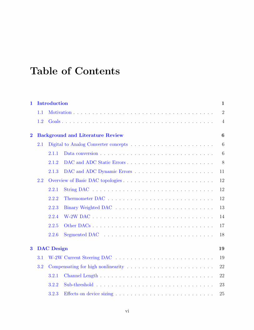
Table of Contents
1 Introduction 1
1.1 Motivation . . . . . . . . . . . . . . . . . . . . . . . . . . . . . . . . . . . . . 2
1.2 Goals . . . . . . . . . . . . . . . . . . . . . . . . . . . . . . . . . . . . . . . . 4
2 Background and Literature Review 6
2.1 Digital to Analog Converter concepts . . . . . . . . . . . . . . . . . . . . . . 6
2.1.1 Data conversion . . . . . . . . . . . . . . . . . . . . . . . . . . . . . . 6
2.1.2 DAC and ADC Static Errors . . . . . . . . . . . . . . . . . . . . . . . 8
2.1.3 DAC and ADC Dynamic Errors . . . . . . . . . . . . . . . . . . . . . 11
2.2 Overview of Basic DAC topologies . . . . . . . . . . . . . . . . . . . . . . . . 12
2.2.1 String DAC . . . . . . . . . . . . . . . . . . . . . . . . . . . . . . . . 12
2.2.2 Thermometer DAC . . . . . . . . . . . . . . . . . . . . . . . . . . . . 12
2.2.3 Binary Weighted DAC . . . . . . . . . . . . . . . . . . . . . . . . . . 13
2.2.4 W-2W DAC . . . . . . . . . . . . . . . . . . . . . . . . . . . . . . . . 14
2.2.5 Other DACs . . . . . . . . . . . . . . . . . . . . . . . . . . . . . . . . 17
2.2.6 Segmented DAC . . . . . . . . . . . . . . . . . . . . . . . . . . . . . 18
3 DAC Design 19
3.1 W-2W Current Steering DAC . . . . . . . . . . . . . . . . . . . . . . . . . . 19
3.2 Compensating for high nonlinearity . . . . . . . . . . . . . . . . . . . . . . . 22
3.2.1 Channel Length . . . . . . . . . . . . . . . . . . . . . . . . . . . . . . 22
3.2.2 Sub-threshold . . . . . . . . . . . . . . . . . . . . . . . . . . . . . . . 23
3.2.3 Effects on device sizing . . . . . . . . . . . . . . . . . . . . . . . . . . 25
vi

3.2.4 Compensation technique . . . . . . . . . . . . . . . . . . . . . . . . . 28
3.3 The Minch and Grinch . . . . . . . . . . . . . . . . . . . . . . . . . . . . . . 30
3.3.1 The Minch . . . . . . . . . . . . . . . . . . . . . . . . . . . . . . . . . 30
3.3.2 The Grinch . . . . . . . . . . . . . . . . . . . . . . . . . . . . . . . . 31
3.4 Complete Segmented Dac (4-bit Binary weighted and 5-bit Unary) . . . . . . 34
3.5 Chip Layout . . . . . . . . . . . . . . . . . . . . . . . . . . . . . . . . . . . . 34
3.6 Single DAC Layout . . . . . . . . . . . . . . . . . . . . . . . . . . . . . . . . 39
3.7 Bit Layout . . . . . . . . . . . . . . . . . . . . . . . . . . . . . . . . . . . . . 39
3.8 Design Summary . . . . . . . . . . . . . . . . . . . . . . . . . . . . . . . . . 40
4 Board Design 41
4.1 Inputs and Outputs . . . . . . . . . . . . . . . . . . . . . . . . . . . . . . . . 41
4.1.1 Input and Output Schematic Overview . . . . . . . . . . . . . . . . . 41
4.1.2 Input and Output Board Layout . . . . . . . . . . . . . . . . . . . . . 41
4.2 Support circuits . . . . . . . . . . . . . . . . . . . . . . . . . . . . . . . . . . 42
4.2.1 Voltage references . . . . . . . . . . . . . . . . . . . . . . . . . . . . . 42
4.2.2 Current Reference . . . . . . . . . . . . . . . . . . . . . . . . . . . . . 47
4.3 Design Summary . . . . . . . . . . . . . . . . . . . . . . . . . . . . . . . . . 47
5 Experimental Results 49
5.1 Test Setup . . . . . . . . . . . . . . . . . . . . . . . . . . . . . . . . . . . . . 49
5.2 Preliminary Evaluation . . . . . . . . . . . . . . . . . . . . . . . . . . . . . . 49
5.3 Results . . . . . . . . . . . . . . . . . . . . . . . . . . . . . . . . . . . . . . . 51
5.3.1 Statistical Average of Results . . . . . . . . . . . . . . . . . . . . . . 53
5.3.2 Complete Characterization of a single W-2W DAC . . . . . . . . . . 54
5.4 Results Discussion . . . . . . . . . . . . . . . . . . . . . . . . . . . . . . . . 55
6 Conclusions 56
6.1 This Work . . . . . . . . . . . . . . . . . . . . . . . . . . . . . . . . . . . . . 56
6.2 Future Work . . . . . . . . . . . . . . . . . . . . . . . . . . . . . . . . . . . . 57
Bibliography 58
vii

Appendices 61
A Schematics . . . . . . . . . . . . . . . . . . . . . . . . . . . . . . . . . . . . . 62
B MATLAB . . . . . . . . . . . . . . . . . . . . . . . . . . . . . . . . . . . . . 74
B.1 Find GPIB Address . . . . . . . . . . . . . . . . . . . . . . . . . . . . 74
B.2 NI DAQ input bits . . . . . . . . . . . . . . . . . . . . . . . . . . . . 74
B.3 INL and DNL of full scale sweep . . . . . . . . . . . . . . . . . . . . 76
Vita 78
viii

List of Tables
1.1 MISA IDAC requirments . . . . . . . . . . . . . . . . . . . . . . . . . . . . . 4
1.2 MISA Biquad requirements . . . . . . . . . . . . . . . . . . . . . . . . . . . 5
2.1 Binary Conversion [Kester (2004)] . . . . . . . . . . . . . . . . . . . . . . . . 7
2.2 DAC Comparison summery . . . . . . . . . . . . . . . . . . . . . . . . . . . 18
3.1 Monte Carlo of 12-bit DAC . . . . . . . . . . . . . . . . . . . . . . . . . . . 25
3.2 Reduced Width[Sperotto et al. (2015)] . . . . . . . . . . . . . . . . . . . . . 28
5.1 Chip 1 W Bias = W2 Bias . . . . . . . . . . . . . . . . . . . . . . . . . . . . 51
5.2 Chip 1 W Bias != W2 Bias . . . . . . . . . . . . . . . . . . . . . . . . . . . 51
5.3 INL of Chip 1 . . . . . . . . . . . . . . . . . . . . . . . . . . . . . . . . . . . 51
5.4 DNL of Chip 1 . . . . . . . . . . . . . . . . . . . . . . . . . . . . . . . . . . 52
5.5 INL and DNL of 2µm DAC of Chip 1,2,3,4 . . . . . . . . . . . . . . . . . . . 52
5.6 INL and DNL of 4µm DAC of Chip 1,2,3,4 . . . . . . . . . . . . . . . . . . . 53
5.7 Average INL and DNL with 100nA full Scale . . . . . . . . . . . . . . . . . . 53
5.8 Average INL and DNL with 400nA full Scale . . . . . . . . . . . . . . . . . . 53
5.9 Completely Optimized 2µ DAC (2.546mV offset) . . . . . . . . . . . . . . . . 54
5.10 DAC requirements comparison . . . . . . . . . . . . . . . . . . . . . . . . . . 55
ix

List of Figures
1.1 MISA 2 Biquad Filter Topology . . . . . . . . . . . . . . . . . . . . . . . . . 3
2.1 Digital-to-Analog Converter (DAC) and Analog-to-Digital Converter (ADC) 7
2.2 Offset and Gain Error . . . . . . . . . . . . . . . . . . . . . . . . . . . . . . 8
2.3 Digital-to-Analog Converter (DAC) Integral nonlinearity (INL) and Analog-
to-Digital Converter (ADC) Integral nonlinearity (INL) . . . . . . . . . . . . 10
2.4 Differential nonlinearity (DNL) . . . . . . . . . . . . . . . . . . . . . . . . . 10
2.5 Settling Time Measurement . . . . . . . . . . . . . . . . . . . . . . . . . . . 11
2.6 String DAC . . . . . . . . . . . . . . . . . . . . . . . . . . . . . . . . . . . . 12
2.7 Fully Decoded DAC . . . . . . . . . . . . . . . . . . . . . . . . . . . . . . . . 13
2.8 Binary Weighted DAC . . . . . . . . . . . . . . . . . . . . . . . . . . . . . . 13
2.9 R-2R DAC . . . . . . . . . . . . . . . . . . . . . . . . . . . . . . . . . . . . . 14
2.10 4-Bit W-2W NMOS Binary Weighted DAC w/ Differential output . . . . . . 14
2.11 Parallel and Series MOSFETs . . . . . . . . . . . . . . . . . . . . . . . . . . 15
2.12 The basic principle of current division . . . . . . . . . . . . . . . . . . . . . . 16
2.13 Segmented Current-Output DACs . . . . . . . . . . . . . . . . . . . . . . . . 18
3.1 Basic Block Diagram . . . . . . . . . . . . . . . . . . . . . . . . . . . . . . . 20
3.2 Simplified PMOS W-2W DAC . . . . . . . . . . . . . . . . . . . . . . . . . . 20
3.3 First INL curve . . . . . . . . . . . . . . . . . . . . . . . . . . . . . . . . . . 21
3.4 Small-signal Mismatch . . . . . . . . . . . . . . . . . . . . . . . . . . . . . . 22
3.5 Second INL curve . . . . . . . . . . . . . . . . . . . . . . . . . . . . . . . . . 24
3.6 INL Sweep data . . . . . . . . . . . . . . . . . . . . . . . . . . . . . . . . . . 26
3.7 INL with unit transistor size of 2µm . . . . . . . . . . . . . . . . . . . . . . 27
x

3.8 4-bit DAC to be tapered . . . . . . . . . . . . . . . . . . . . . . . . . . . . . 28
3.9 Reduced Tapered INL . . . . . . . . . . . . . . . . . . . . . . . . . . . . . . 29
3.10 Final INL of 12-bit W-2W . . . . . . . . . . . . . . . . . . . . . . . . . . . . 29
3.11 Ladder ranks . . . . . . . . . . . . . . . . . . . . . . . . . . . . . . . . . . . 30
3.12 Minch current mirror . . . . . . . . . . . . . . . . . . . . . . . . . . . . . . . 31
3.13 Minch I-V curve . . . . . . . . . . . . . . . . . . . . . . . . . . . . . . . . . . 32
3.14 Minch current Gain . . . . . . . . . . . . . . . . . . . . . . . . . . . . . . . . 32
3.15 Grinch current mirror . . . . . . . . . . . . . . . . . . . . . . . . . . . . . . . 33
3.16 Op-Amp used in Grinch . . . . . . . . . . . . . . . . . . . . . . . . . . . . . 33
3.17 Closed loop Cut-off (Top) Open-loop Bode plot (Bottom) . . . . . . . . . . . 35
3.18 Complete DAC . . . . . . . . . . . . . . . . . . . . . . . . . . . . . . . . . . 36
3.19 System Block Diagram . . . . . . . . . . . . . . . . . . . . . . . . . . . . . . 36
3.20 DAC biasing and OTA . . . . . . . . . . . . . . . . . . . . . . . . . . . . . . 37
3.21 Chip Layout . . . . . . . . . . . . . . . . . . . . . . . . . . . . . . . . . . . . 38
3.22 DAC Layout . . . . . . . . . . . . . . . . . . . . . . . . . . . . . . . . . . . . 39
3.23 Bit Layout . . . . . . . . . . . . . . . . . . . . . . . . . . . . . . . . . . . . . 39
3.24 Bit Layout . . . . . . . . . . . . . . . . . . . . . . . . . . . . . . . . . . . . . 40
4.1 Test Board . . . . . . . . . . . . . . . . . . . . . . . . . . . . . . . . . . . . . 42
4.2 Board Inputs and Outputs . . . . . . . . . . . . . . . . . . . . . . . . . . . . 43
4.3 Actual Test Board . . . . . . . . . . . . . . . . . . . . . . . . . . . . . . . . 44
4.4 LT3020 Adjustable LDO . . . . . . . . . . . . . . . . . . . . . . . . . . . . . 45
4.5 LT3020 1.8V . . . . . . . . . . . . . . . . . . . . . . . . . . . . . . . . . . . . 45
4.6 TPS799 Fixed LDO . . . . . . . . . . . . . . . . . . . . . . . . . . . . . . . . 45
4.7 TPS799 3.3V . . . . . . . . . . . . . . . . . . . . . . . . . . . . . . . . . . . 46
4.8 LT1963 Adjustable 1.5A Voltage Source . . . . . . . . . . . . . . . . . . . . 46
4.9 TPS7A3001 Adjustable Negative Voltage Source . . . . . . . . . . . . . . . . 46
4.10 Voltage input Rails for 100nA current source . . . . . . . . . . . . . . . . . . 47
4.11 LTC6082 nanoAmp Current Source . . . . . . . . . . . . . . . . . . . . . . . 48
5.1 Test Setup . . . . . . . . . . . . . . . . . . . . . . . . . . . . . . . . . . . . . 50
xi

5.2 Chip 1 Characterization where W bias = 2W bias . . . . . . . . . . . . . . . 50
5.3 Chip 1 Characterization where W bias != 2W bias . . . . . . . . . . . . . . . 50
5.4 2µm DAC Characterization of Chip 1,2,3,4 . . . . . . . . . . . . . . . . . . . 52
5.5 4µm DAC Characterization of Chip 1,2,3,4 . . . . . . . . . . . . . . . . . . . 52
5.6 FOM of Bits per Area . . . . . . . . . . . . . . . . . . . . . . . . . . . . . . 54
5.7 FOM and power consumption . . . . . . . . . . . . . . . . . . . . . . . . . . 55
6.1 Symmetrical Ladder Network . . . . . . . . . . . . . . . . . . . . . . . . . . 57
A1 12-bit PMOS W-2W Schematic . . . . . . . . . . . . . . . . . . . . . . . . . 62
A2 Grinch Schematic . . . . . . . . . . . . . . . . . . . . . . . . . . . . . . . . . 63
A3 Op-Amp Schematic . . . . . . . . . . . . . . . . . . . . . . . . . . . . . . . . 63
A4 Minch Schematic . . . . . . . . . . . . . . . . . . . . . . . . . . . . . . . . . 64
A5 Complete Schematic . . . . . . . . . . . . . . . . . . . . . . . . . . . . . . . 64
A6 RAZA Schematic . . . . . . . . . . . . . . . . . . . . . . . . . . . . . . . . . 65
A7 W-2W DAC Test Bed . . . . . . . . . . . . . . . . . . . . . . . . . . . . . . 66
A8 Top Level Schematic . . . . . . . . . . . . . . . . . . . . . . . . . . . . . . . 67
A9 Voltage Source Schematic . . . . . . . . . . . . . . . . . . . . . . . . . . . . 68
A10 Current References Schematic . . . . . . . . . . . . . . . . . . . . . . . . . . 69
A11 Current References Schematic 2 . . . . . . . . . . . . . . . . . . . . . . . . . 70
A12 Solder Mask . . . . . . . . . . . . . . . . . . . . . . . . . . . . . . . . . . . . 71
A13 Power Plane . . . . . . . . . . . . . . . . . . . . . . . . . . . . . . . . . . . . 72
A14 3D overlay . . . . . . . . . . . . . . . . . . . . . . . . . . . . . . . . . . . . . 73
xii

List of Nomenclature
ADC Analog-to-Digital Convertor
CMOS Complementary metal–oxide–semiconductor
DAC Digital-to-Analog Convertor
DAQ Data Acquisition
DNL Differential Nonlinearity
DSP Digitial Signal Processing
FET Field-effect transistor
INL Integral Nonlinearity
LSB Least Significant Bit
MCU Microcontroller
MOSFET Metal-oxide-semiconductor Field Effect Transistor
MSB Most Significant Bit
NMOS N-channel MOSFET
Op− Amp Operational Amplifier
OTA Operational Transconductance Amplifier
PCB Printed Circuit Board
PMOS P-channel MOSFET
xiii

Chapter 1
Introduction
Analog and Digital signal conversion is one of the most important topics under the umbrella
of electrical engineering for a myriad of reasons and the applications for analog-to-digital
converters (ADCs) and digital-to-analog converters (DACs) has been growing without
bounds since the introduction of the ENIAC project in 1942[1,DCH] Cases of data conversion
have been seen as far back as 18th Century Turkey under the Ottoman Empire to meter
the water supply [Kester (2004)]. Today, Digital Signal Processing(DSP) is the dominant
method of analyzing and/or transforming a signal and analog methods have fallen by the
way side because digital performance has grown to a much greater extent than analog signal
processing methods. In terms of efficiency however, analog signal processing has shown time
and time again that it is still relevant when it comes to low power applications.
As in the case of the DSP, electronics progressed through the last half a century by moving
a large portion of it from analog to digital. Modern digital design and analog design are
often viewed as two separate entities with two separate approaches to solve signal processing
and/or control functions, but as the world becomes more mobile and more retaliate on battery
technology, a resurgence of analog design has happened over the last couple of decades to
fill the need for ultra low power devices. Also as device manufacturing becomes smaller,
digital design as been encroached on by analog (physical) limitations of devices. The future
of electrical engineering has reached a point where the standard short hand equations are no
longer valid. The industry can no longer ignore things such as short channel effects or relying
on the devices that need to be operated above the threshold voltage. Circuit design is now
1
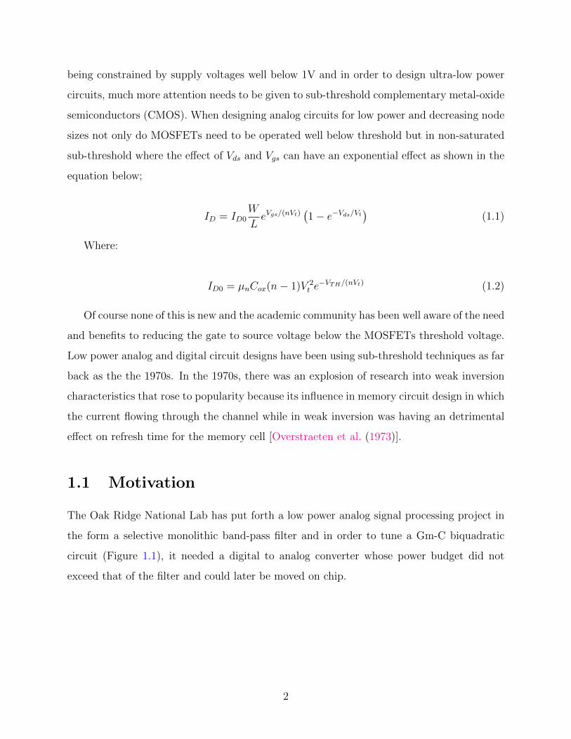
being constrained by supply voltages well below 1V and in order to design ultra-low power
circuits, much more attention needs to be given to sub-threshold complementary metal-oxide
semiconductors (CMOS). When designing analog circuits for low power and decreasing node
sizes not only do MOSFETs need to be operated well below threshold but in non-saturated
sub-threshold where the effect of Vds and Vgs can have an exponential effect as shown in the
equation below;
ID = ID0W
LeVgs/(nVt)
(1− e−Vds/Vt
)(1.1)
Where:
ID0 = µnCox(n− 1)V 2t e
−VTH/(nVt) (1.2)
Of course none of this is new and the academic community has been well aware of the need
and benefits to reducing the gate to source voltage below the MOSFETs threshold voltage.
Low power analog and digital circuit designs have been using sub-threshold techniques as far
back as the the 1970s. In the 1970s, there was an explosion of research into weak inversion
characteristics that rose to popularity because its influence in memory circuit design in which
the current flowing through the channel while in weak inversion was having an detrimental
effect on refresh time for the memory cell [Overstraeten et al. (1973)].
1.1 Motivation
The Oak Ridge National Lab has put forth a low power analog signal processing project in
the form a selective monolithic band-pass filter and in order to tune a Gm-C biquadratic
circuit (Figure 1.1), it needed a digital to analog converter whose power budget did not
exceed that of the filter and could later be moved on chip.
2

Figure 1.1: MISA 2 Biquad Filter Topology
3

1.2 Goals
The goals of this work are:
� Research qualified DAC topologies
� Provide a low-power DAC
� Try to meet the specifications as provided by ORNL in table 1.1
� Verify currents are with 1 percent of table 1.2
� Find the effects of the DAC in sub-threshold
� Investigate the validity of sizing constraints
Table 1.1: MISA IDAC requirments
Resolution(nA) Current (nA)0.0451 540.67
4
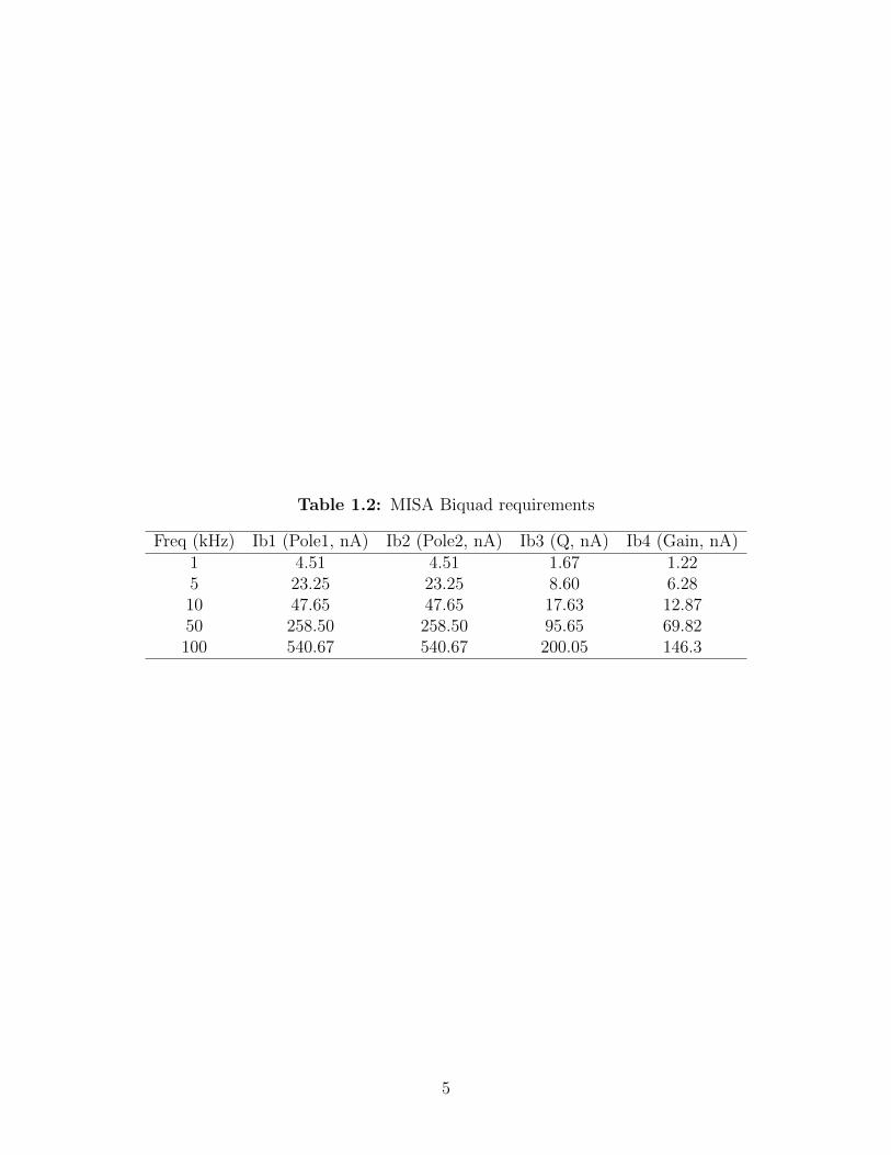
Table 1.2: MISA Biquad requirements
Freq (kHz) Ib1 (Pole1, nA) Ib2 (Pole2, nA) Ib3 (Q, nA) Ib4 (Gain, nA)1 4.51 4.51 1.67 1.225 23.25 23.25 8.60 6.2810 47.65 47.65 17.63 12.8750 258.50 258.50 95.65 69.82100 540.67 540.67 200.05 146.3
5

Chapter 2
Background and Literature Review
2.1 Digital to Analog Converter concepts
2.1.1 Data conversion
Data conversion is used in many industry specific applications such as PCM communications,
data telemetry systems, audio/video signal systems, data logging systems and sampled-data
control systems. Data conversion is the process of translation between real world physical
parameters and quantized data used in computation, control or transmission. An example of
data conversion is binary conversion, as shown in table 2.1. The table shows the translation
from a digital binary representation to an analog output voltage. More specifically it is used
to represent a continuously variable physical signal into a finitely time-sampled data series
for use between the physical and virtual world [Eugene L. Zueh (1987)].
Analog-to-digital converters (ADCs) are used to translate analog input variables such as
voltages and currents into a digital representation of data used for processing, transmitting,
storing or controlling. Digital-to-analog converters (DACs) are used to translate stored or
processed digital data into real world analog outputs used for control or further analog
processing [Kester (2004)]. The symbols typically used for an ADC and DAC are shown in
figure 2.1
6

Table 2.1: Binary Conversion [Kester (2004)]
Base 10 Scale +10V FS Binary Gray15 15/16 9.375V 1111 100014 14/16 8.750V 1110 100113 13/16 8.125V 1101 101112 12/16 7.500V 1100 101011 11/16 6.875V 1011 111010 10/16 6.250V 1010 11119 9/16 5.625V 1001 11018 8/16 5.000V 1000 11007 7/16 4.375V 0111 01006 6/16 3.750V 0110 01015 5/16 3.125V 0101 01114 4/16 2.500V 0100 01103 3/16 1.875V 0011 00102 2/16 1.250V 0010 00111 1/16 0.625V 0001 00010 0 0.000V 0000 0000
Figure 2.1: (DAC) Digital-to-Analog Converter and (ADC) Analog-to-Digital Converter
7

Figure 2.2: Offset Error (A), Gain Error(B) and Full Scale Error(C)
2.1.2 DAC and ADC Static Errors
The static or absolute precision of a DAC is predominantly set by three types of errors:
� Offset errors
� Gain errors
� Linearity (INL/DNL)
The offset error, as shown in Figure 2.2A above, is the vertical difference between the
ideal transfer function and the output of the DAC that is usually measured when all ”0”s
are applied to the input causing it to be referred to as zero-scale error. Gain errors, as
shown in Figure 2.2B, is the difference in slope of the actual output of the DAC from the
ideal transfer function of a straight line placed the end-points[Kester (2004)]. Gain error is
calculated using the equation 2.1. Together, offset and gain error create full-scale error as
shown in figure 2.2C.
Gain Error (%) = 100
[V111 + VFS − Vos
2Vrs − 1LSB− 1
](2.1)
Normally offset errors and gain errors are not of high importance because in many
applications it is easy to compensate or adjust for during the design. The most important
contribution to errors in data conversion circuits are linearity errors. The two types of
linearity errors are integral nonlinearity (INL) and differential nonlinearity (DNL)[Kester
(2004)].
8

Integral nonlinearity, sometimes referred to as ’relative accuracy’, is the maximum
difference in terms of least-significant-bits (LSBs), between the ideal straight line and
measured transfer function. Depending on the source, INL can be defined in different ways
and two of the most common definitions for INL are used with one containing full-scale error
information.
� Best straight-line INL - The closest depiction of true linearity of an ADC or DAC
because in contains information about offset errors and gain errors. It also contains
information about the position of the straight line transfer function in relation to the
actual transfer function but is not defined to a specific point. Best fit INL approach
is the nearest approximation to a repeatable best fit line that does not change when
full-scale errors occur[van de Plasche (1994)].
� End-point INL - Defined by connecting a straight line from the LSB to the MSB of
the converter’s complete transfer function that clearly defines the position of straight
line [van de Plasche (1994)].
The preferred approached is the best straight-line method as it shows more favorable
results. INL as depicted in figure 2.3 is calculated using the following equation when gain
errors and offset errors have been zeroed out;
INL = | [VD − VZERO) /NLSB−IDEAL]−D|, where 0 < D < 2N−1 (2.2)
where VD is the voltage at the output code D and N is the number in bits of resolution,
VZERO is the minimum voltage at the lower output code, and VLSB−IDEAL is the ideal
distance between two succeeding output codes [van de Plasche (1994)].
9

Figure 2.3: Digital-to-Analog Converter (DAC) Integral nonlinearity (INL) and Analog-to-Digital Converter (ADC) Integral nonlinearity (INL)
Differential nonlinearity as depicted in figure 2.4 is calculated using the following equation
when gain errors and offset errors have been zeroed out;is the maximum difference between
actual output and the ideal output between adjacent DAC codes, as shown in Figure 2.5
below and is calculated using equation 2.3. In general, if the error in DNL is assured to be
less than 1 LSB than the DAC is considered monotonic. Monotonicity is defined as always
increasing as code increases which signifies that there are no missing codes [Kester (2004)].
DNL = |[(ND+1 − VD) /NLSB−IDEAL − 1]| , where 0 < D < 2N − 2 (2.3)
Figure 2.4: Differential nonlinearity (DNL)
10

Figure 2.5: Settling Time Measurement [Kester (2004)]
2.1.3 DAC and ADC Dynamic Errors
Shown in figure 2.5 are a few dynamic errors or AC errors associated with data converters
that were largely mitigated by system design and/or application. These types of errors
can be attributed to conversion rate errors and are not of much importance when design a
”static” DAC.
� Settling time - The maximum time needed for a transition to establish on the desired
value[Razavi (1995)]
� Glitch impulse area - The maximum glitch area that happens on the output when
changing the input[Razavi (1995)]
� Latency - The system delay between between the input and output[Razavi (1995)]
� Slew Rate - The maximum rate the output can be switched[Razavi (1995)]
11

Figure 2.6: String DAC
2.2 Overview of Basic DAC topologies
2.2.1 String DAC
The string DAC as shown in figure 2.6 is the simplest DAC topology with origin back to
the 1800s with the Kelvin Divider. It is a simple voltage divider that has an output that
is inherently monotonic and it’s linearity is completed dependent on the matching of the
restive elements. The string DAC has very little switching glitch due to only 2 switches
being operated on no matter the output transition, but the major deficiency of a sting DAC
is the amount of switched and resistors needed to obtain a high resolution. Until recently,
with the advent of much smaller node sizes for IC design, the string DAC was not commonly
used. Now though, it is used quite often for medium resolution applications or a component
of a much more complex data converter [Kester (2004)].
2.2.2 Thermometer DAC
The thermometer DAC or fully decoded DAC is comparable to a current-mode string DAC
with switchable current sources tied to the output. A thermometer DAC can use voltage
referenced resistors or active currents sources as shown in figure 2.7. This structure is also
inherently monotonic like the string DAC regardless of the current source matching because
as the code increasing, subsequent current sources are not switched off. Just like the string
DAC, the fully decoded current mode DAC has not been relevant until high density IC
fabrication made it practical[Kester (2004)].
12

Figure 2.7: Fully Decoded DAC
Figure 2.8: Binary Weighted DAC
2.2.3 Binary Weighted DAC
The binary weighted DAC as shown in figure 2.8 was a topology that was proposed to
simplify the switch matrix needed for fully decoded DACs by allowing the input code to be
the same as the switch matrix needed. The major problem with the binary weighted DAC
is the fact that it is not inherently monotonic [Kester (2004)].
The most popular binary weighted DAC is the R-2R ladder DAC as shown below in
figure 2.9. The primary benefit of the R-2R architecture over previous binary weighted
architectures is the fact that the output impedance remands constant as can be shown using
Thevenin’s theorem. The circuit topology is a basic voltage divider using resistors with
values of R and 2 ∗ R and uses the principle of superposition and consecutive voltage or
current division to arrive at the final value as shown in the equation below;
Vout = VRefRf
R
[B1
21+B2
22+B3
23+ · · ·+ Bn
2n
](2.4)
13

Figure 2.9: R-2R DAC
Figure 2.10: 4-Bit NMOS W-2W Binary Weighted DAC with Differential output [Guptaet al. (2009)]
2.2.4 W-2W DAC
The W-2W DAC is a binary weighted current steering DAC architecture that is comparable
to a R-2R in design and function. The W-2W DAC is presented as solving the biggest
problem with binary weighted DACs which is current mismatch[Gupta et al. (2009)]. Figure
2.10 shows a 4-Bit NMOS W-2W Binary Weighted DAC with Differential output presented
by Baker to mitigate the problems of mismatch.
At first glance, the W-2W topology appears to use MOSFETs in linear region to function
as resistors creating the same resistive ladder divider as on R-2R but the W-2W DAC uses
current division instead. That is to say, linearity of the W-2W structure is dependent
on the relative matching of the I-V curve and is not dependent on the MOSFETs having
similar resistive values. The implementation of the W-2W DAC, sometimes referred to as
14

Figure 2.11: Parallel and Series MOSFETs
the binary-weighted W-2W current mirror topology, works on two conventions that will be
briefly discussed below[Sperotto et al. (2015)].
� Equivalent sizing of parallel and series MOSFETs
� The Current Division Principle
Equivalent sizing of parallel and series MOSFETs
Equivalent sizing of parallel and series MOSFETs as shown in figure 2.11 uses the principle
that two MOSFETs of the same width and length connected in parallel will have the same
attributes as a single device that has a double the width, while the same two MOSFETs
were connected in series would have the same attributes as a single device with double the
length[Baker (2010)].
The MOS Current division principle
The MOS Current division principle as presented in ”An Inherently Linear and Compact
MOST-Only Current Division Technique” by Bult and Geelen, states the ratio of I1 and I2
in the figure 2.12 below is [Bult and Geelen (1993)]:
� Constant and independent of Iin
� Not dependent on voltages Va and Vb
� Not dependent on either device being in saturation
� Not dependent on either device being in strong or weak inversion
15
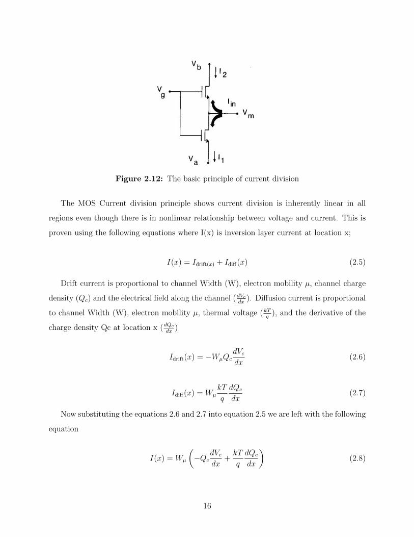
Figure 2.12: The basic principle of current division
The MOS Current division principle shows current division is inherently linear in all
regions even though there is in nonlinear relationship between voltage and current. This is
proven using the following equations where I(x) is inversion layer current at location x;
I(x) = Idrift(x) + Idiff(x) (2.5)
Drift current is proportional to channel Width (W), electron mobility µ, channel charge
density (Qc) and the electrical field along the channel (dVcdx
). Diffusion current is proportional
to channel Width (W), electron mobility µ, thermal voltage (kTq
), and the derivative of the
charge density Qc at location x (dQc
dx)
Idrift(x) = −WµQcdVcdx
(2.6)
Idiff(x) = WµkT
q
dQc
dx(2.7)
Now substituting the equations 2.6 and 2.7 into equation 2.5 we are left with the following
equation
I(x) = Wµ
(−Qc
dVcdx
+kT
q
dQc
dx
)(2.8)
16

Assuming the current is the same across the channel, we can integrate from x=0 to x=L
as such;
I · L = W
∫ x=L
x=0
−µ(QcdVcdx− kT
q
dQc
dx
)dx (2.9)
Now if you divide by the length and change the running variable to voltage along the
channel you will get the follow equation;
ID = (W/L)
∫ vc=vS
Vc=vD
µ
(Qc −
kT
q
dQc
dVc
)dVc (2.10)
where
µ
(Qc −
kT
q
dQc
dVc
)= f (VG, Vc) (2.11)
As you can now see, current matching between the two MOSFETs is completely dependent on
the symmetry of the device (interchanging the Source and Drain have no effect on magnitude)
and the dimensions. This gives us the following equation;
∆Id1
∆Id2
= −W1/L1
W2/L2
(2.12)
which denotes the inherently linear aspect of current division and the unresponsiveness
to such things as the body effect, mobility reduction and most importantly that is valid
for regions (strong inversion, weak inversion, linear region, and saturation)[Bult and Geelen
(1993)].
2.2.5 Other DACs
Listed below are a few commonly used DACs for high resolution that were considered but
ultimately not used because sampling errors, switch complexity, transient noise, hold mode
feed through, deglitch overhead and most notably digital overhead. By using a simpler DAC
topology, not only can power be saved and dynamic errors reduced but DAC architectures
such as the W-2W are not subject to offset and gain errors by the natural of it being confined
17

Figure 2.13: Segmented Current-Output DACs
Table 2.2: DAC Comparison summery
Fully Decoded Dacs Binary DACs1. Monotincity2. Small DNL errors
Advantages1. Low power consumption2. Small number of signals
1. Digital decoding power2. Increased control signals
Disadvantages1. Not inherently monotonic2. Larger DNL errors
to a Full-Scale value. This decision is also justified by it’s static application not needing a
high conversion rate.
� Oversampling Interpolating DAC
� Ramp/Counting/Slope DAC
� Cyclic Serial DAC
2.2.6 Segmented DAC
When designing a DAC architecture, there are many pros and cons of each topology. Table
2.2 shows a quick comparison between fully decoded DAC and binary DACs but in practice
it is normal to use multiple types of architectures together. This is done by using one
topology for the MSBs and another for the LSBs. This practice is called segmentation and
you can segment any types of DACs together. Figure 2.13 shows a 3-bit thermometer/fully
decoded DAC segmented with a 4-bit binary decoded DAC and this allows your to used the
advantages of both [Kester (2004)].
18

Chapter 3
DAC Design
The basic block diagram in figure 3.1 shows the 25pA resolution W-2W DAC presented in
the research. It is a 12-bit current mode ladder DAC with a full scale current of 100nA that is
segmented with a 5-bit current steering unary DAC to provide an additional current range.
The DAC block diagram shows the three building blocks used to meet the specifications
required. The three building blocks are the W-2W DAC, the Minch current mirror and the
Grinch current mirror.
3.1 W-2W Current Steering DAC
Shown in figure 3.2 is a 4-Bit simplified version of the final 12-bit DAC that was implemented
with PMOS. In the figure above there are two ladder ranks; the ”W” ladder rank and the
”W2” ladder rank with W/L always equal to 1 to use a unit transistor size. The W rank
consists of Q15, Q11, Q2, and Q7 and uses 10 fingers, while the W2 rank consists of Q13, Q9,
Q1, and Q5 and uses 20 fingers per devices. Using Cadence, the 12-bit DAC was simulated
using random unit size transistors and a full-scale current on 100µA. Cadence gave the
following INL curve that showed a maximum INL of 21 LSBs. Looking at the Figure 3.3, it
can been shown that there is a systematic error causing such a large INL. The figure shows
the largest error is due to the MSB and the second largest error is due to the second MSB.
The first reason for the systemic error is the fact that each bit has twice the effect on
error as the succeeding bit simply because it contributes twice the amount of current to
19

Figure 3.1: Basic DAC Block Diagram
Figure 3.2: Simplified PMOS W-2W DAC
20

Figure 3.3: First INL curve
21

Figure 3.4: Small-signal Mismatch[Sperotto et al. (2015)]
output. Using the figure 3.4 it can be shown that statistical mismatch of each transistor can
be estimated using the ratioed amount of current through each branch. The second reason
for the systematic error, also due to successive current division through the each bit of the
DAC, is each bit being at different inversion level [Sperotto et al. (2015)].
3.2 Compensating for high nonlinearity
3.2.1 Channel Length
One Critical aspect of analog circuit design is finding the minimum channel length that
reduces the effect on carrier velocity saturation. The carrier velocity saturation effect
becomes very considerable when the channel length becomes small enough that the carrier
velocity and longitudinal electric field are not proportional, so we must calculate a large
enough length to mitigate this effect. Using the following equations for the carrier velocity
effect on mobility we can approximate the channel length needed [Sodini et al. (1984)];
µsat =µ0√
1 + (Ex/EC)2(3.1)
where µ0 is the low field mobility,Ex is the electric field that is along the channel(Ex =
VDS/L), EC is the critical electric field (EC = vsat/µ) and vsat is the carrier saturation
velocity[Sodini et al. (1984)].
Lmin =VDS
EC√
1(1−ε)2 − 1
(3.2)
22

The result from the equations above give us an approximate value of L = 10µm for the
proposed DAC. The value for the unit transistor sized was changed to reflect the calculated
value above and the Cadence simulation was ran again with very little change to the linearity
of the proposed DAC. Although the effects of channel length were small at this point in the
design process, the effect can be completely removed by eliminating the channel. This is
achieved by running the devices in sub-threshold.
3.2.2 Sub-threshold
Despite the fact that designing in sub-threshold is a valid design region, it is often a last
resort and the biasing scheme for a sub-threshold device is exponentially more sensitive than
a device above threshold hold as seen in the different equations for ID depending on the
region. First we needed to look at the termination voltage, which is set by the Grinch
building block. Setting the termination voltage is what controls the drain to source voltage
(VDS) of the ladder. The termination voltage of the proposed DAC was raised to mid-rail of
900mV to lower the difference between the gate and source voltage. Then the gate voltage
(VG) was also subsequently lower from 1.8V down to 530mV using a method of trial and error
in the Cadence. The figure below shows the INL results of the DAC ran at sub-threshold.
Figure 3.5 shows the greatest effect to linearity of the proposed DAC at this point is
running it in sub-threshold. The reason being because the second order effects such as
Threshold Voltage Variations, Hot Carrier Effects and Velocity Saturation are considerably
mitigated. The threshold voltage mismatch is a larger driving force for current mismatch
in the topology and although first order effects of mobility variations are irrelevant due to
the nature of the current division principle as stated above, it helps with transversal field
increases and surface scattering effects when gate oxides become thin in deep submicron
processes[Sperotto et al. (2015)].
23
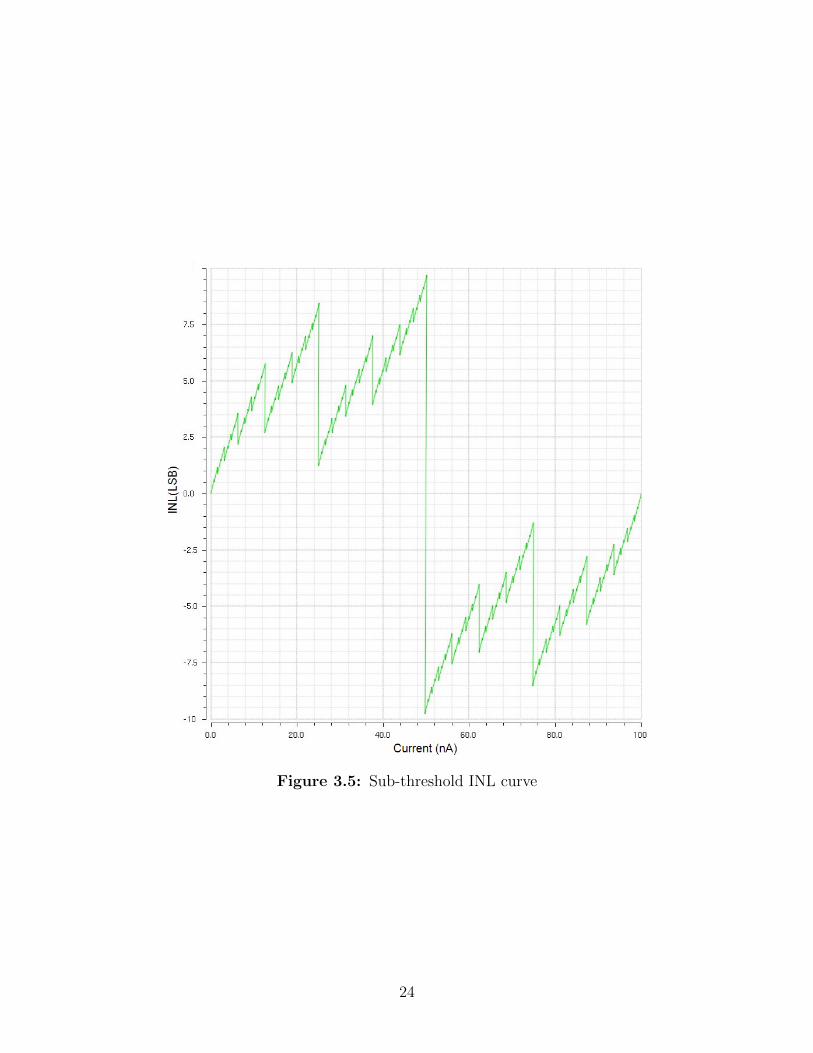
Figure 3.5: Sub-threshold INL curve
24
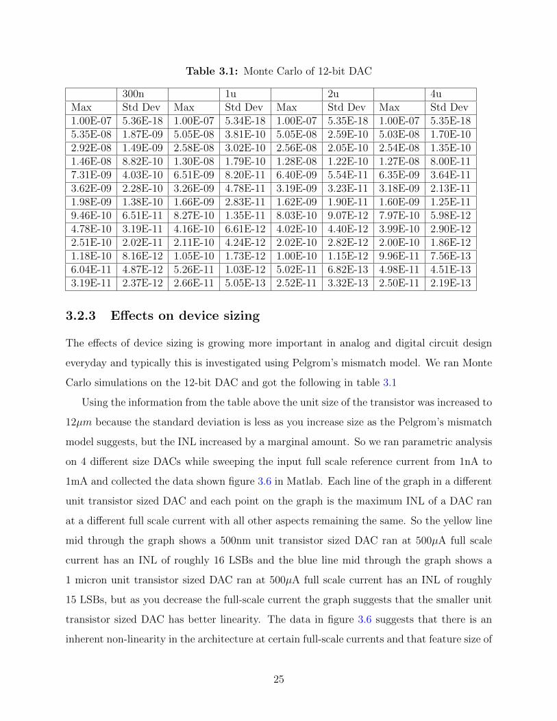
Table 3.1: Monte Carlo of 12-bit DAC
300n 1u 2u 4uMax Std Dev Max Std Dev Max Std Dev Max Std Dev1.00E-07 5.36E-18 1.00E-07 5.34E-18 1.00E-07 5.35E-18 1.00E-07 5.35E-185.35E-08 1.87E-09 5.05E-08 3.81E-10 5.05E-08 2.59E-10 5.03E-08 1.70E-102.92E-08 1.49E-09 2.58E-08 3.02E-10 2.56E-08 2.05E-10 2.54E-08 1.35E-101.46E-08 8.82E-10 1.30E-08 1.79E-10 1.28E-08 1.22E-10 1.27E-08 8.00E-117.31E-09 4.03E-10 6.51E-09 8.20E-11 6.40E-09 5.54E-11 6.35E-09 3.64E-113.62E-09 2.28E-10 3.26E-09 4.78E-11 3.19E-09 3.23E-11 3.18E-09 2.13E-111.98E-09 1.38E-10 1.66E-09 2.83E-11 1.62E-09 1.90E-11 1.60E-09 1.25E-119.46E-10 6.51E-11 8.27E-10 1.35E-11 8.03E-10 9.07E-12 7.97E-10 5.98E-124.78E-10 3.19E-11 4.16E-10 6.61E-12 4.02E-10 4.40E-12 3.99E-10 2.90E-122.51E-10 2.02E-11 2.11E-10 4.24E-12 2.02E-10 2.82E-12 2.00E-10 1.86E-121.18E-10 8.16E-12 1.05E-10 1.73E-12 1.00E-10 1.15E-12 9.96E-11 7.56E-136.04E-11 4.87E-12 5.26E-11 1.03E-12 5.02E-11 6.82E-13 4.98E-11 4.51E-133.19E-11 2.37E-12 2.66E-11 5.05E-13 2.52E-11 3.32E-13 2.50E-11 2.19E-13
3.2.3 Effects on device sizing
The effects of device sizing is growing more important in analog and digital circuit design
everyday and typically this is investigated using Pelgrom’s mismatch model. We ran Monte
Carlo simulations on the 12-bit DAC and got the following in table 3.1
Using the information from the table above the unit size of the transistor was increased to
12µm because the standard deviation is less as you increase size as the Pelgrom’s mismatch
model suggests, but the INL increased by a marginal amount. So we ran parametric analysis
on 4 different size DACs while sweeping the input full scale reference current from 1nA to
1mA and collected the data shown figure 3.6 in Matlab. Each line of the graph in a different
unit transistor sized DAC and each point on the graph is the maximum INL of a DAC ran
at a different full scale current with all other aspects remaining the same. So the yellow line
mid through the graph shows a 500nm unit transistor sized DAC ran at 500µA full scale
current has an INL of roughly 16 LSBs and the blue line mid through the graph shows a
1 micron unit transistor sized DAC ran at 500µA full scale current has an INL of roughly
15 LSBs, but as you decrease the full-scale current the graph suggests that the smaller unit
transistor sized DAC has better linearity. The data in figure 3.6 suggests that there is an
inherent non-linearity in the architecture at certain full-scale currents and that feature size of
25

Figure 3.6: INL Sweep data
the unit transistor only mitigates this to a certain degree in different regions. This inherent
non-linearity in the architecture is positioned around the inversion level of each bit in the
DAC. Simply put, the W-2W will have better linearity if you can guarantee every bit has a
similar inversion level and INL gets better as the difference between each bit gets smaller.
After the parametric analysis we needed to investigate this further so we decided to
fabricate a DAC with three different size unit transistor to verify the possibility that a lower
full-scale current and a smaller unit size transistor could result in better linearity. After
reducing the full-scale current to 100nA from 100µA and reducing the unit transistor size to
2µm the maximum INL was approximately 5 LSBs as shown in figure 3.7.
26

Figure 3.7: INL with unit transistor size of 2µm
27

Table 3.2: Reduced Width[Sperotto et al. (2015)]
Transistors Original Width Reduced WidthM1,M2,M3 4µm 3.85µm
M4,M5,M6,M7 4µm 3.9µmM8,M9,M10,M11 4µm 3.95µm
M12,M13,M14,M15,M16,M17 4µm 4µm
Figure 3.8: 4-bit DAC to be tapered[Sperotto et al. (2015)]
3.2.4 Compensation technique
The last step in compensating for the systematic nonlinearity was creating an offset that
was larger for the MSB and smaller for the LSB. A typical way to accomplish this, as found
in the literature, was an approach that creates what is called a tapered W-2W DAC (figure
3.8). This approach sizes the MSBs transistors in a tapered manner with the MSB having a
smallest width and the second MSB having a slightly smaller width than the third MSB as
shown in table 3.2 [Sperotto et al. (2015)].
The results of this approach is in the following INL graph in figure 3.9;
This technique was abandoned because it would make the layout more complicated and
impossible to be symmetrical. A different technique was used, which was to bias the the
gate voltage of W and W2 ladder rank separately. This a very simple technique that works
because it will have a much greater effect on the current of the MSB then it will on the
second MSB and so on until you get to the LSB. This is for the same reason the offset is
mostly contributed by the MSB and second most contributed by the second MSB, successive
28
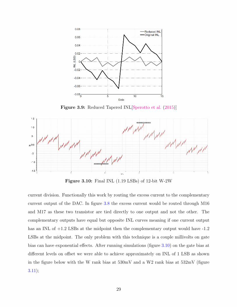
Figure 3.9: Reduced Tapered INL[Sperotto et al. (2015)]
Figure 3.10: Final INL (1.19 LSBs) of 12-bit W-2W
current division. Functionally this work by routing the excess current to the complementary
current output of the DAC. In figure 3.8 the excess current would be routed through M16
and M17 as these two transistor are tied directly to one output and not the other. The
complementary outputs have equal but opposite INL curves meaning if one current output
has an INL of +1.2 LSBs at the midpoint then the complementary output would have -1.2
LSBs at the midpoint. The only problem with this technique is a couple millivolts on gate
bias can have exponential effects. After running simulations (figure 3.10) on the gate bias at
different levels on offset we were able to achieve approximately on INL of 1 LSB as shown
in the figure below with the W rank bias at 530mV and a W2 rank bias at 532mV (figure
3.11);
29
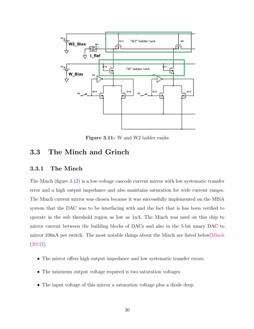
Figure 3.11: W and W2 ladder ranks
3.3 The Minch and Grinch
3.3.1 The Minch
The Minch (figure 3.12) is a low-voltage cascode current mirror with low systematic transfer
error and a high output impedance and also maintains saturation for wide current ranges.
The Minch current mirror was chosen because it was successfully implemented on the MISA
system that the DAC was to be interfacing with and the fact that is has been verified to
operate in the sub threshold region as low as 1nA. The Minch was used on this chip to
mirror current between the building blocks of DACs and also in the 5-bit unary DAC to
mirror 100nA per switch. The most notable things about the Minch are listed below[Minch
(2012)];
� The mirror offers high output impedance and low systematic transfer errors.
� The minimum output voltage required is two saturation voltages.
� The input voltage of this mirror a saturation voltage plus a diode drop.
30

Figure 3.12: Minch current mirror
� The bias current, Ib, does not adaptability track Iin and Iin does not represent an
maximum limit of Ib.
The plot below in Figure 3.13 show the I-V curve at different bias currents of 100nA,
10nA, and 1nA. The figure 3.14 below shows the current gain with the current at the input
swept from 100pA to 1µA and then the current at the output is measured with the worst
current gain decreasing to 100pA which is 90 percent of the lowest current setting[Long
(2018)].
3.3.2 The Grinch
The Grinch as shown in figure 3.15 is a modified Minch used to create the termination voltage
for the W-2W DAC and to create the current sink to bias the OTAs of the MISA system.
Essentially the Grinch places the Op-Amp below inside the Minch. The operational
amplifier in the figure 3.16 is a current biased input differential pair that is compensated
using class AB output stage and was also successfully implemented on the MISA chip.
31

Figure 3.13: Minch I-V curve
Figure 3.14: Minch Current Gain
32

Figure 3.15: Grinch current mirror
Figure 3.16: Op-Amp used in Grinch[Long (2018)]
33

Shown in figure 3.17 is the simulation results of the Op-Amp biased at 100nA with a 15pF
and 10M Ohm load configured in unity gain. The top of the figure shows a cutoff frequency
of the closed-loop gain to be approximately 900kHz at -3db. While the bottom of the figure
shows the open loop results of the simulation that was conducted with the same 15pF and
10M Ohm load and a DC feedback network. The Bode plot shows a a crossover frequency of
approximately 30kHz with the phase at the crossover frequency of approximately 89 degrees
at an open-loop gain of around 73dB [Long (2018)].
3.4 Complete Segmented Dac (4-bit Binary weighted
and 5-bit Unary)
This section shows a simplified version of the proposed complete DAC. Shown in the figure
3.18 is a 4-bit Binary weighted W-2W DAC that is segmented with a 5-bit Unary current
range selection DAC. The actual DAC experimentally tested has a 12-bit Binary weighted
W-2W DAC but functions exactly the same. This is followed by a system block diagram
(figure 3.19) describing the summation of the 2 segmented DACs at the output of the Grinch
and a Cadence schematic (figure 3.20) of the final implementation of the DAC biasing an
operational transconductance amplifier (OTA) from MISA.
3.5 Chip Layout
This section overviews the layout of the 4 DACs on the chip. The figure 3.21 shows entire
chip with 4 DACs with 3 different DAC sizes and also three extra Minch current mirrors in
order to bias the support circuitry for the 4 DACs. The three extra Minch current mirrors
are used to insure the input reference current for the three building blocks (W-2W DAC,
Grinch, Minch DAC) are all the same. In the red and green squares are 2 2µm unit transistor
DACs. In the blue square is a 4µm unit transistor DAC and in the pink square is a 1µm
unit transistor DAC.
34

Figure 3.17: Closed loop Cut-off (Top) Open-loop Bode plot (Bottom)
35

Figure 3.18: Complete DAC
Figure 3.19: System Block Diagram
36

Figure 3.20: DAC biasing an OTA
37

Figure 3.21: The RAZA Layout (2.5mm by 2.5mm)
38
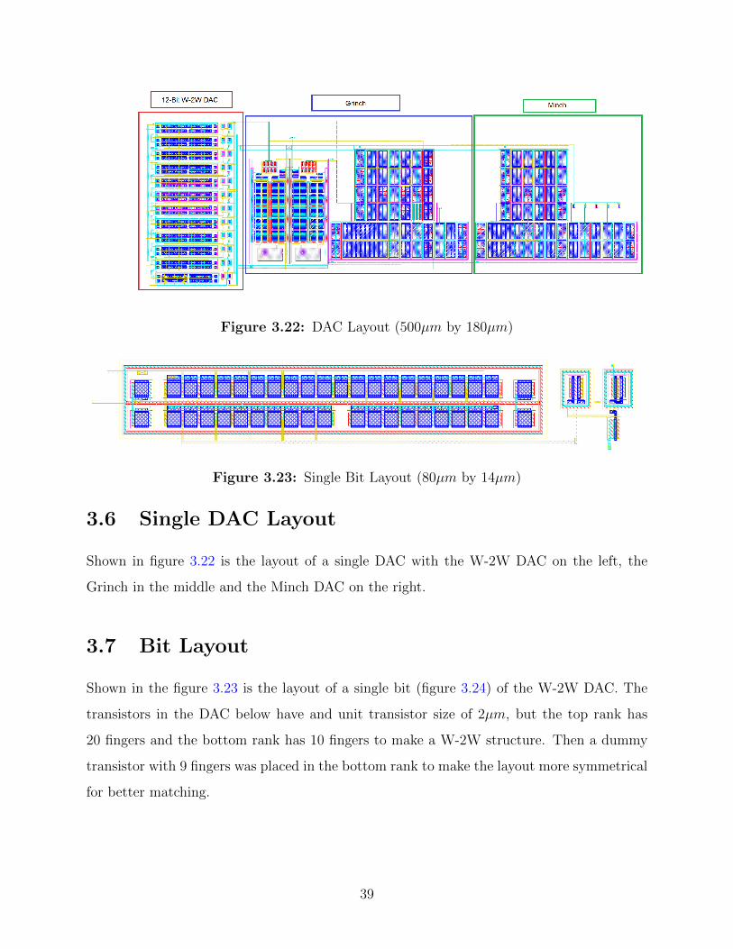
Figure 3.22: DAC Layout (500µm by 180µm)
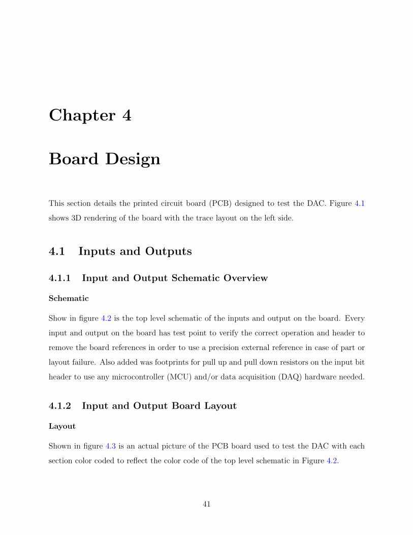
Figure 3.23: Single Bit Layout (80µm by 14µm)
3.6 Single DAC Layout
Shown in figure 3.22 is the layout of a single DAC with the W-2W DAC on the left, the
Grinch in the middle and the Minch DAC on the right.
3.7 Bit Layout
Shown in the figure 3.23 is the layout of a single bit (figure 3.24) of the W-2W DAC. The
transistors in the DAC below have and unit transistor size of 2µm, but the top rank has
20 fingers and the bottom rank has 10 fingers to make a W-2W structure. Then a dummy
transistor with 9 fingers was placed in the bottom rank to make the layout more symmetrical
for better matching.
39

Figure 3.24: Single Bit Schematic
3.8 Design Summary
During the design phase for the proposed DAC there were many iterations of the design
including more complex topologies with considerable digital overhead that were ultimately
decided against for reason discussed at the end of chapter 2. Also different types of
compensation techniques from the literature were attempted to try and improve the linearity
before deciding to bias the ladder ranks separately to use complementary output to route
the offset current to the other branch. Although the W-2W architecture was proven to be
insensitive to first order effects due to the nature of the current division principle, the second
order effects needed to be investigated and considered when the simulation data suggested
that the proposed DAC’s linearity could be improved upon by biasing the ladder far below the
threshold voltage and decreasing the unit transistor size. In summary the effect of biasing
and device sizing as it pertained to linearity of the W-2W topology took a considerable
amount of time and effort to understand. In the end, multiple Cadence simulations and
parametric analysis showed that the inversion level of devices is more nuanced than just
strong, moderate, and weak inversion. The inversion levels of the devices are on a continuum
and the closer the inversion levels for each succeeding bit is to each other the closer the
tangential lines of the bias points on the I-V curve will be, which signifies better current
matching.
40
Chapter 4
Board Design
This section details the printed circuit board (PCB) designed to test the DAC. Figure 4.1
shows 3D rendering of the board with the trace layout on the left side.
4.1 Inputs and Outputs
4.1.1 Input and Output Schematic Overview
Schematic
Show in figure 4.2 is the top level schematic of the inputs and output on the board. Every
input and output on the board has test point to verify the correct operation and header to
remove the board references in order to use a precision external reference in case of part or
layout failure. Also added was footprints for pull up and pull down resistors on the input bit
header to use any microcontroller (MCU) and/or data acquisition (DAQ) hardware needed.
4.1.2 Input and Output Board Layout
Layout
Shown in figure 4.3 is an actual picture of the PCB board used to test the DAC with each
section color coded to reflect the color code of the top level schematic in Figure 4.2.
41

Figure 4.1: Test Board
4.2 Support circuits
This section details the components used for supporting the DAC such as voltage references
and current references.
4.2.1 Voltage references
LT3020
The LT3020 (figure 4.4) is a linear, low dropout regulator that is capable of regulating from
0.2V to 9.5V with a minimum input supply voltage of 0.9V. LT3020 devices can supply
100mA of output current and with a dropout voltage typically around 150mV. This Low-
Dropout (LDO) regulator was used for 1.8V sources (figure 4.5) needed for the chip and used
to set the Grinch voltage that tunes the W-2W termination voltage[Technology (2012)].
42

Figure 4.2: Top level Schematic
43
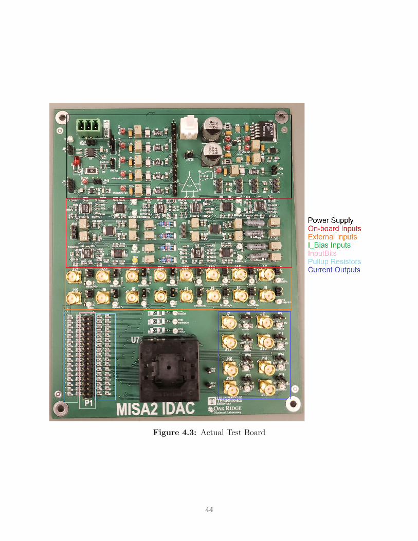
Figure 4.3: Actual Test Board
44

Figure 4.4: LT3020 Adjustable LDO
Figure 4.5: LT3020 1.8V
TPS799
The TPS799 (figure 4.6) is a ultra low noise, low-quiescent current LDO regulator with high
PSRR used for powering the ESD Diode on the chip (figure 4.7) [Instruments (2015)].
Figure 4.6: TPS799 Fixed LDO
45

Figure 4.7: TPS799 3.3V
Figure 4.8: LT1963 Adjustable 1.5A Voltage Source
LT1963
The LT1963 (figure 4.8) is a LDO regulator with a dropout voltage of 340mV while also
being capable of delivering 1.5A. It is used for the +2.5V voltage supply rails for 100nA
current source references[Technology (1999)].
TPS7A3001
The TPS7A3001 (figure 4.9) is a high-accuracy, ultra low noise negative linear regulator
capable of delivering 200mA used for high-precision instrumentation application. The
TPS7A3001 is used for the -2.5V rail of the 100nA current source reference[Instruments
(2011)].
Figure 4.9: TPS7A3001 Negative Voltage Source
46

Figure 4.10: Voltage Rails for 100nA current source
2.5V and -2.5V voltages rails
Shown below in figure 4.10 is the schematic used for the +2.5V and -2.5V supply rails of
100nA current source reference.
4.2.2 Current Reference
The LTC6082 Ts a dual package LTC6081 that is a rail-to-rail input/output swing, low noise
CMOS operational amplifier that also has low drift and low offset. The LTC6082 uses 330µA
of current on a 3 volt supply rail and was designed for precision signal conditioning which
was perfect for the application. Using the application notes of the LTC6082 the following
schematic figure 4.11 was provided of a current source reference capable of sourcing or sinking
1nA with a total error of 10pA [Technology (2001)].
4.3 Design Summary
The final test board for the DAC only used different types of voltage/current sources and
references but there are multiple copies of each source or reference to be able to switch in
and out different references depending on which DAC size and full-scale current that was
being tested. Ideally you could share a single voltage reference and a single current reference
to all DACs but the test board was designed with plenty of option in mind.
47

Figure 4.11: LTC6082 nanoAmp Current Source
48

Chapter 5
Experimental Results
This section will discuss the test setup used to evaluate the proposed DAC and give a brief
summary of the results.
5.1 Test Setup
Shown in figure 5.1 is a block diagram of the basic test setup. The chip is sectioned by two
sets of DACs. The first set, labeled DAC set A, is comprised of A 2µm and a 4µm unit
transistor sized DAC and the second set, labeled DAC set B, is comprised of A 2µm and a
1µm unit transistor sized DAC. Each set of DACs has the same bit inputs to be able test
two different sized DACs at the same time. A MATLAB script changes the bit inputs on
a DAC set and measures the current output of the two different sized DACs through the
Keithley model 2636B source meter which is capable a precision down to femtoAmps(fA).
5.2 Preliminary Evaluation
The preliminary evaluation was to characterize the chip with and without the compensation
method of separating the W and W2 ladder rank bias. Shown in Figure 5.2 below is chip 1
with a single gate voltage bias of 520mV for both ladder ranks and a single 100nA current
reference. This is followed by Figure 5.3, which show the effects to the linearly of the
proposed DAC by creating a different VGS for the W and W2 ladder ranks.
49

Figure 5.1: Test Setup
Figure 5.2: Chip 1 Characterization where W bias = W2 bias
Figure 5.3: Chip 1 Characterization where W bias != 2W bias
50

Table 5.1: Chip 1 W Bias = W2 Bias
DAC Unit Transistor INL DNL1µm 2.7316 5.15142µm 2.2475 4.17912µm 2.2267 4.03534µm 2.8497 5.3214
Table 5.2: Chip 1 W Bias != W2 Bias
DAC Unit Transistor INL DNL1µm 1.3957 2.45712µm 0.6955 1.18162µm 0.6621 1.07134µm 1.8815 2.6234
The following tables (tables 5.1, 5.2, 5.3 and 5.4) show a side by side comparison of Figure
5.2 and 5.3 to verify the validity of the compensation method discussed in chapter 3.2.4.
As the simulation data suggests, this compensation scheme decreases the INL of the 2µm
DAC from 2.2475 LSBs down to 0.6955 LSBs and the DNL from 4.1791 LSBs to 1.1816
LSBs. There is also the same trend in all other unit transistor sized DACs.
5.3 Results
After the preliminary evaluation, we tested for the random variation between of each DAC
size on multiple chips. Shown in figure 5.4 is the INL and DNL of the one of the 2µm unit
transistor sized DACs followed by the INL and DNL of the 4µm unit transistor sized DAC
(figure 5.5). This is followed by a table comparing the results (tables 5.5 and 5.6).
Although some variation was to be assumed, the experimental data had a much wider
statistical variation than expected. This can be mostly attributed to the on board ladder
Table 5.3: INL of Chip 1
DAC Unit Transistor W Bias = 2W Bias W Bias != 2W Bias1µm 2.7316 1.39572µm 2.2475 0.69882µm 2.2267 0.66214µm 2.8497 1.8815
51

Table 5.4: DNL of Chip 1
DAC Unit Transistor W Bias = 2W Bias W Bias != 2W Bias1µm 5.1514 2.43792µm 4.1791 1.18162µm 4.0353 1.07134µm 5.3642 2.6234
Figure 5.4: 2µm DAC Characterization of Chip 1,2,3,4
Figure 5.5: 4µm DAC Characterization of Chip 1,2,3,4
Table 5.5: INL and DNL of 2µm DAC of Chip 1,2,3,4
Chip INL (LSB) DNL (LSB)Chip 1 1.1631 1.6041Chip 2 1.3177 1.7251Chip 3 1.6647 2.6722Chip 4 1.9879 2.8660
52

Table 5.6: INL and DNL of 4µm DAC of Chip 1,2,3,4
Chip INL (LSB) DNL (LSB)Chip 1 2.9346 3.9054Chip 2 2.3433 4.4111Chip 3 3.9367 5.0918Chip 4 2.1678 3.0965
Table 5.7: Average INL and DNL with 100nA full Scale
DAC Unit Transistor INL(LSB) DNL(LSB)1µm 1.4567 2.54842µm 0.9254 1.35434µm 1.7651 2.5547
rank biases moving from run to run. Even though the biases were set using precision 15
turn potentiometers, a difference in a few nV could have drastic effects on the linearity of
the DAC.
5.3.1 Statistical Average of Results
After characterizing 4 different chips it was apparent that there was large variance in the
INL and DNL between each chip, so 16 chips were characterized and an average was taken to
approximate the linearity of each DAC unit transistor size. Shown in the table 5.7 below is
the final linearity of each DAC unit transistor size at a full-scale current of 100nA, followed
by table 5.8 that shows the same DACs ran at a full-scale current of 400nA.
Comparing the 2 tables of experimental data above with the simulated parametric
analysis of the full-scale current sweep in Figure 3.6, it can be shown that they follow
the same trend, which is the linearity of the W-2W topology get betters as the full-scale
current gets lower. However, this is only true to a certain point where process variations
Table 5.8: Average INL and DNL with 400nA full Scale
DAC Unit Transistor INL(LSB) DNL(LSB)1µm 2.3154 3.45872µm 2.0445 2.65414µm 2.6541 3.4754
53

Figure 5.6: FOM of Bits per Area
Table 5.9: Completely Optimized 2µ DAC (2.546mV offset)
Process Bits ENOB Power Area INL DNL
0.18 µ 12 10.2 85µW 450µm by 185 µm 0.6405 1.0841
such as random dopant fluctuations or the noise floor begins to overshadow matching of the
successive current division at such low levels.
5.3.2 Complete Characterization of a single W-2W DAC
This section condenses the results of the 2µm unit transistors DAC on chip 7, which gave
the best linearity results and compares them to a few others DACs found in the literature.
The DAC tested below was characterized after using the precision current source to tune
ladder rank offset voltage to the theoretical maximum INL value by slowly moving the offset
in picovolts after each linearity test. Listed in table 5.9 is a complete characterization of the
2µm unit transistors DAC followed by two different figures of merit (FOM). For comparison
the following figure of merits were chosen to reflect the most important attributes to the
MISA DAC project, which are area and power. The first FOM in the figure 5.6 is to show
the comparison of area between the DACs by using the number of bits for each DAC 2N
divided by the area of the DAC after scaling them all to a theoretical 1µ process. This is
followed by figure 5.7 which shows the FOM using the area and power consumption.
54

Figure 5.7: FOM of power consumption
Table 5.10: DAC requirements comparison
Ideal current (nA) Measured current (nA) Percent difference1.22 1.2075 1.201.67 1.6776 0.504.51 4.4874 0.516.28 6.2961 0.528.60 8.6009 0.0112.87 12.8867 0.1317.63 17.6450 0.0923.25 23.2536 0.0247.65 47.6723 0.0569.82 69.8287 0.0195.65 95.6726 0.033
5.4 Results Discussion
The following shows if the proposed DAC architecture in the research is a valid option the
the MISA system. Using the the DAC requirements as provided by ORNL in the chapter
1, a comparison table is made to verify the if proposed DACs experimental verified current
output is within the 1 percent of the needed value.
The table 5.10 shows that the maximum percent difference 1.2 at 1.22nA and a minimum
percent difference of 0.01 at 69.82nA. This metric shows that the required percent difference
was failed by mere 0.2 percent.
55

Chapter 6
Conclusions
6.1 This Work
In conclusion this work discusses the design and testing of a sub-threshold CMOS digital-to-
analog converter used to tune the bias current GM-C biquadratic filter circuit for a low-power
multichannel spectral analysis system. The proposed DAC is a 12-bit MOSFET only W-2W
DAC segmented with a 5-bit unary current range selection capable of 25pA of resolution
and a full-scale current of 600nA. While researching qualified DAC topologies to meet the
specifications of the current-mode DAC needed, many attributes such as low-power biasing
schemes and sizing constraints were investigated in order to determine its effectiveness in a
comparable environment in which it would be used. During the simulation phase of design
it was put forth that lower full-scale currents and bias voltages could possibly improve the
linearity of the proposed DAC and that seemed to run counter to conventional ideas of
MOSFET current matching. After fabrication and testing of the DAC it was discovered
that matching inversion levels had a considerable effect on the successive current matching
from bit to bit of the W-2W structure. Also in the thesis is a novel compensation technique of
separating the ladder rank bias to improve the linearity using the offset in the complementary
current. The results of the DAC proposed in this research was compared to a table of the
ideal currents needed by the MISA system in chapter 5.4 and had a maximum percent
difference of 1.2 percent and a minimum percent difference of 0.01 percent. Although the
56
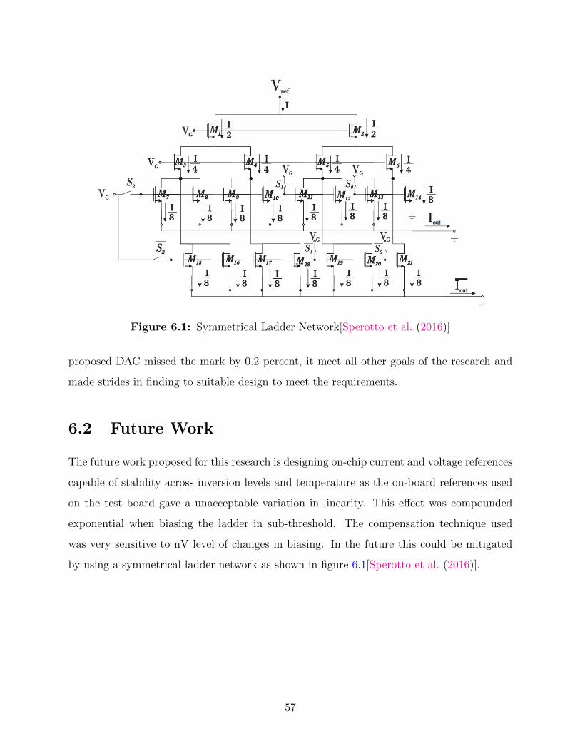
Figure 6.1: Symmetrical Ladder Network[Sperotto et al. (2016)]
proposed DAC missed the mark by 0.2 percent, it meet all other goals of the research and
made strides in finding to suitable design to meet the requirements.
6.2 Future Work
The future work proposed for this research is designing on-chip current and voltage references
capable of stability across inversion levels and temperature as the on-board references used
on the test board gave a unacceptable variation in linearity. This effect was compounded
exponential when biasing the ladder in sub-threshold. The compensation technique used
was very sensitive to nV level of changes in biasing. In the future this could be mitigated
by using a symmetrical ladder network as shown in figure 6.1[Sperotto et al. (2016)].
57

Bibliography
58
I. Sperotto, H. Klimach, and S. Bampi, “Design and linearity analysis of a m-2m dac for
very low supply voltage,” Conference 2015 IEEE International Conference on Electronics,
Circuits, and Systems (ICECS), Dec. 2015. ix, 15, 22, 23, 28, 29
W. Kester, Data Conversion Handbook. Newnes, 2004. ix, 1, 6, 7, 8, 10, 11, 12, 13, 18
R. V. Overstraeten, G. Declerck, and G. Broux, “Inadequacy of the classical theory of the mos
transistor operating in weak inversion,” IEEE Transactions on Electron Devices, vol. 20,
no. 12, pp. 1150–1153, Dec. 1973. 2
D. Eugene L. Zueh, Data Acquisition and Conversion. Datel, 1987. 6
R. van de Plasche, Integrated Analog-to-Digital and Digital-to-Analog Converters. Kluwer
Academic Publishers, 1994. 9
B. Razavi, Principles of Data Conversion System Design. A JOHN WILEY and SONS,
1995. 11
S. Gupta, V. Saxena, and R. J. Baker, “W-2w current steering dac for programming phase
change memory,” Conference Microelectronics and Electron Devices, pp. 1–4, May 2009.
14
R. J. Baker, CMOS Circuit Design, Layout, and Simulation. A JOHN WILEY and SONS,
2010. 15
K. Bult and G. J. G. M. Geelen, “An inherently linear and compact most-only current
division technique,” IEEE Journal of Solid-State Circuits, vol. 27, no. 12, pp. 1730 – 1735,
Dec. 1993. 15, 17
C. Sodini, P.-K. Ko, and J. Moll, “The effect of high fields on mos device and circuit
performance,” IEEE Transactions on Electron Devices, vol. 31, no. 10, pp. 1386 – 1393,
Oct. 1984. 22
B. A. Minch, “A simple low-voltage cascode current mirror with enhanced dynamic
performance,” in 2012 IEEE Subthreshold Microelectronics Conference (SubVT). IEEE,
2012, pp. 1–3. 30
59

G. B. Long, “A monolithic gm-c filter based very low power, programmable, and multi-
channel harmonic discrimination system using analog signal processing,” Master’s thesis,
University of Tennessee, 12 2018. 31, 33, 34
L. Technology, “Lt3020/lt3020,” 2012. 42
T. Instruments, “Tps799,” 2015. 45
L. Technology, “Lt1963 series,” 1999. 46
T. Instruments, “Tps7a3001-ep,” 2011. 46
L. Technology, “Ltc6081/ltc6082,” 2001. 47
I. Sperotto, H. Klimach, and S. Bampi, “Symmetrical mos ladder dac with improved linearity
for ultra-low voltage applications,” Conference 6th Workshop on Circuits and System
Design (WCAS 2016), Aug. 2016. 57
60

Appendices
61

Figure A1: 12-bit PMOS W-2W Schematic
A Schematics
62

Figure A2: Grinch Schematic
Figure A3: Op-Amp Schematic
63

Figure A4: Minch Schematic
Figure A5: Complete Schematic
64
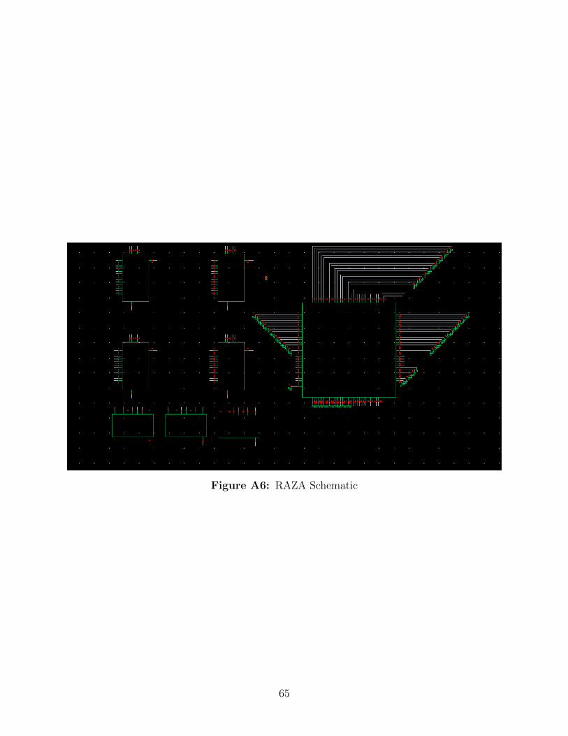
Figure A6: RAZA Schematic
65

Figure A7: W-2W DAC Test Bed
66

Figure A8: Top Level Schematic
67

Figure A9: Voltage Source Schematic
68

Figure A10: Current References Schematic
69

Figure A11: Current References Schematic 2
70

Figure A12: Solder Mask
71

Figure A13: Power Plane
72

Figure A14: 3D overlay
73

B MATLAB
B.1 Find GPIB Address
%% Find GPIB address for source meter and DAQ
function [dev , id] = find_gpib_dev (vendor , boardindex ,
primaryaddress)
dev = instrfind ('Type', 'gpib', 'BoardIndex ', boardindex , '
PrimaryAddress ', primaryaddress , 'Tag', '');
if isempty(dev)
dev = gpib (vendor , boardindex , primaryaddress);
else
fclose (dev);
dev = dev(1);
end
fopen (dev);
id = id_dev (dev);
fclose (dev);
end
B.2 NI DAQ input bits
%% USing the NI DAQ to change input bits
pause on;
%% Establish connection
[keithley , idkeithley] = find_gpib_dev ('NI', 0, 3);
fopen (keithley);
74
%% change Execel save file
filename = 'DacData1uBChip1offset4mvEXTERN.xlsx';
q = daq.getDevices;
s = daq.createSession('ni');
addDigitalChannel(s,'Dev3','port0/line0 :7','OutputOnly ');
addDigitalChannel(s,'Dev3','port1/line0 :7','OutputOnly ');
addDigitalChannel(s,'Dev3','port2/line7 ','OutputOnly ');
%create bits
table = dec2bin (0:(2^12 -1)) - '0';
%flip bit for proper sequence
b = flip(table ,2);
%matrix of zero for minch unary
x = zeros (4096 ,5);
%create matrix of 12DAC + 5 minch Bits
z = cat(2,b,x);
m = 1;
for m = 1:4096
n = z(m,:);
outputSingleScan(s,n);
pause (0.005);
fprintf(keithley ,'print(smua.measure.i(smua.nvbuffer1))');
d(m) = str2double(fgets(keithley));
end
data = d';
xlswrite(filename ,data)
75
fclose (keithley);
B.3 INL and DNL of full scale sweep
sweep1nTo1mDNL500nA = sweep1nTo1mDNL500n (: ,2:2: end);
sweep1nTo1mDNL500nMAX =max(abs(sweep1nTo1mDNL500nA));
sweep1nTo1mDNL1uA = sweep1nTo1mDNL1u (: ,2:2: end);
sweep1nTo1mDNL1uMAX =max(abs(sweep1nTo1mDNL1uA));
sweep1nTo1mDNL2uA = sweep1nTo1mDNL2u (: ,2:2: end);
sweep1nTo1mDNL2uMAX =max(abs(sweep1nTo1mDNL2uA));
sweep1nTo1mDNL4uA = sweep1nTo1mDNL4u (: ,2:2: end);
sweep1nTo1mDNL4uMAX =max(abs(sweep1nTo1mDNL4uA));
sweep1nTo1mDNL8uA = sweep1nTo1mDNL8u (: ,2:2: end);
sweep1nTo1mDNL8uMAX =max(abs(sweep1nTo1mDNL8uA));
sweep1nTo1mINL500nA = sweep1nTo1mINL500n (: ,2:2: end);
sweep1nTo1mINL500nMAX =max(abs(sweep1nTo1mINL500nA));
sweep1nTo1mINL1uA = sweep1nTo1mINL1u (: ,2:2: end);
sweep1nTo1mINL1uMAX =max(abs(sweep1nTo1mINL1uA));
sweep1nTo1mINL2uA = sweep1nTo1mINL2u (: ,2:2: end);
sweep1nTo1mINL2uMAX =max(abs(sweep1nTo1mINL2uA));
sweep1nTo1mINL4uA = sweep1nTo1mINL4u (: ,2:2: end);
sweep1nTo1mINL4uMAX =max(abs(sweep1nTo1mINL4uA));
76

sweep1nTo1mINL8uA = sweep1nTo1mINL8u (: ,2:2: end);
sweep1nTo1mINL8uMAX =max(abs(sweep1nTo1mINL8uA));
plot(sweep1nTo1mDNL1uMAX ,'DisplayName ','sweep1nTo1mDNL1uMAX ');
hold on;
plot(sweep1nTo1mDNL4uMAX ,'DisplayName ','sweep1nTo1mDNL4uMAX ');
plot(sweep1nTo1mDNL500nMAX ,'DisplayName ','sweep1nTo1mDNL500nMAX
');
plot(sweep1nTo1mDNL8uMAX ,'DisplayName ','sweep1nTo1mDNL8uMAX ');
hold off;
plot(sweep1nTo1mINL500nMAX ,'DisplayName ','sweep1nTo1mINL500nMAX
');hold on;
plot(sweep1nTo1mINL1uMAX ,'DisplayName ','sweep1nTo1mINL1uMAX ');
plot(sweep1nTo1mINL2uMAX ,'DisplayName ','sweep1nTo1mINL2uMAX ');
plot(sweep1nTo1mINL4uMAX ,'DisplayName ','sweep1nTo1mINL4uMAX ');
plot(sweep1nTo1mINL8uMAX ,'DisplayName ','sweep1nTo1mINL8uMAX ');
hold off;
77

Vita
Spencer Raby was born in Jacksonville, Arkansas on February 16. 1987 and graduated high
school at Southern Wayne in Dudley, NC in 2005. After High School, Spencer join the Navy
as an Aircraft Electrician and upon completing his service he entered Pellissippi Community
College where transferred to the University of Tennessee in the fall of 2014 to pursue an
undergraduate degree in Electrical Engineering. He graduated in the Spring of 2017 with
a Bachelor of Science in Electrical Engineering and was encouraged to stay for a Master’s
Degree in Electrical Engineering under the advisement of Professor Benjamin J. Blalock in
the Integrated Circuits and Systems Laboratory (ICASL). During his time under Professor
Blalock, he gained experience in printed circuit board (PCB) design along with designing
and test procedures for low-power mixed-signal circuits. While pursuing his post graduate
studies he also participated in an internship at Texas Instruments in Knoxville, TN where
is worked with the design verification team to test battery charging systems and help write
testing documentation for future TI battery management systems. After this thesis project
he will graduate from the University of Tennessee and transition to design verification job
at Texas Instruments.
78


![API 2W [1993]](https://img.dokumen.tips/doc/110x75/577cd4db1a28ab9e78994d52/api-2w-1993.jpg)


