Embed Size (px)
Citation preview

A CASCADED INVERTER FOR SINGLE-PHASE GRID
CONNECTED PHOTOVOLTAIC SYSTEM
RANJITA KATNAL (109EE0300)
Department of Electrical Engineering
National Institute of Technology Rourkela
A CASCADED INVERTER FOR SINGLE-PHASE GRID
CONNECTED PHOTOVOLTAIC SYSTEM

- 2 -
A CASCADED INVERTER FOR SINGLE-PHASE GRID
CONNECTED PHOTOVOLTAIC SYSTEM
A Thesis submitted in partial fulfillment of the requirements for the degree of
Bachelor of Technology in “Electrical Engineering”
By
RANJITA KATNAL (109EE0300)
Under guidance of
Prof. SOMNATH MAITY
Department of Electrical Engineering
National Institute of Technology
Rourkela-769008 (ODISHA)
May-2013

- 3 -
DEPARTMENT OF ELECTRICAL ENGINEERING
NATIONAL INSTITUTE OF TECHNOLOGY, ROURKELA
ODISHA, INDIA-769008
CERTIFICATE
This is to certify that the thesis entitled “A Cascaded Inverter for Single-phase Grid-
connected Photovoltaic System”, submitted by Ranjita Katnal (Roll. No. 109EE0300) in
partial fulfilment of the requirements for the award of Bachelor of Technology in Electrical
Engineering during session 2012-2013 at National Institute of Technology, Rourkela. A
bonafide record of research work carried out by them under my supervision and guidance.
The candidates have fulfilled all the prescribed requirements.
The Thesis which is based on candidates’ own work, have not submitted elsewhere for a
degree/diploma.
In my opinion, the thesis is of standard required for the award of a bachelor of technology degree
in Electrical Engineering.
Place: Rourkela
Dept. of Electrical Engineering Prof.Somnath Maity
National institute of Technology Assistant Professor
Rourkela-769008

a
ACKNOWLEDGEMENTS
On the submission of my thesis report of “A cascaded Inverter for single-phase grid-connected
system”, I would like to extend my gratitude and sincere thanks to my supervisor Prof.
Somnath Maity, Asst. Professor of the Department of Electrical Engineering, NIT Rourkela for
his essential advice, support and constant motivation at every step of this project in the past year.
I am indebted to him for his esteemed guidance starting from formation of the problem statement
to final derivation and insights for the solution.
I also extend my gratitude to the researchers and engineers whose hours of toil has produced the
papers and theses that I have utilized in my project.
Ranjita Katnal
B.Tech (Electrical Engineering)

b
Dedicated to
My beloved parents

1
ABSTRACT
The Photo Voltaic (PV) energy system, used in this project, is a very new concept in use,
which is gaining immense popularity due to increasing importance to research on alternative
sources of energy over depletion of the conventional fossil fuels all around the world. The
systems which are being developed extract energy from the sun in the most efficient manner and
suit them to the available loads without affecting their performance.
In this project, The design and control issues associated with the development of a 1.8
kW prototype single-phase grid-connected photovoltaic system a multilevel cascaded inverter are
discussed in this project. For the current controller a ramp time zero average current error control
algorithm combined with an optimized cyclic switching sequence is suggested. Simulation
results have been presented to demonstrate the suitability of the control method. Simulation
results exhibits improved performance under the presence of harmonics and the studied system is
modeled and simulated in the MATLAB/Simulink.
2
CONTENTS
Abstract 1
Contents 2
List of Figures 4
List of Tables 6
CHAPTER 1
INTRODUCTION
1.1 Motivation 8
1.2 PV Energy Generation Concepts 9
1.2.1 Grid-connected Applications 9
1.2.2 Stand Alone Applications 9
1.3 Organization of Thesis 9
CHAPTER 2
PV ARRAY CHARACTERISTICS
2.1 Introduction 12
2.2 Photovoltaic Modules 12
2.3 Photovoltaic array 13
2.4 PV array Modelling 13
2.5 Inverters 16
2.6 MOSFETS 18
2.7 I-V Characteristics of Solar cell 21
2.8 Maximum Power Point Tracking 22
2.8.1 Incremental Conductance Method 25

3
2.9 Conclusion 27
CHAPTER-3
SYSTEM DESCRIPTION
3.1 Introduction 29
3.2 Filters 30
3.2.1 L Filters 30
3.2.2 LC Filters 31
3.2.3 LCL Filters 31
3.2.3.1 LCL Filter Design 31
3.3 Grid Synchronization 33
3.3.1 Control structures for grid connected systems 34
3.4 Current Controller 36
3.5 DC Voltage Controller 37
3.6 Conclusion 40
CHAPTER-4
SIMULATION RESULTS
4.1 Introduction 42
4.2 PV Module 42
4.3 Overall Experimental Circuit 47
4.4 Conclusion 49
CHAPTER-5
CONCLUSION AND FUTURE WORK
5.1 Conclusion 51
5.2 Future Work 51
References

4
LIST OF FIGURES
Fig. No Name of the Figure Page. No.
1 Schematic diagram of a simple photovoltaic system 12
2 PV cell single diode equivalent circuit diagram 14
3 Overall model of a PV cell 15
4 A typical stand-alone inverter 17
5 Inverter for grid connected PV 17
6 Schematic diagram of a MOSFET 19
7 The graphical relational between the Drain current and drain to source voltage 20
8 I-V Characteristics at cell temperature of 25°C 22
9 I-V characteristics under wide operating conditions 23
10 Direct Coupled Method 23
11 Basic components of a maximum power pointer tracker 24
12 Typical characteristic curve of a solar cell 25
13 Basic idea of incremental conductance method 26
14 flowchart of ICM method 27
15 Overall system used 29
16 Example of the cascaded inverter output voltage. 30
17 Equivalent circuit diagram 32
18 Model of LCL Filter 32
19 PI controller 36
20 Hysteresis Controller 37
21 ZACE controller 37
22 Dc voltage Loop 38
23 Modified current control loop 39
24 Voltage control loop. 40
25 overall method 42
26 I-V curve 44
27 I-V curve in MATLAB SIMULINK 45
28 P-V curve 45

5
29 Inverter Output voltage 46
30 DC bus voltage 46
31 PV array output 47
32 Overall circuit 48
33 PV array block 48
34 Dc link voltage 49

6
LIST OF TABLES
Table. No. Name of the Table Page. No.
1.1 Comparison of 30 inverters (23 with transformer, 7 transformerless)
for single-phase grid-connected PV systems 8

7
CHAPTER1
Introduction

8
1.1 MOTIVATION:
In the past, various different inverter topologies have been suggested or are currently
used for low power, single-phase grid-connected photovoltaic (PV) Systems. A common
technology in use is a full-bridge inverter in combination with a Line-frequency transformer.
The transformer, however, is not an essential requirement and Inverters without transformers
offer several advantages. A recent European Market survey [1] shows that transformerless
Inverters are advantageous with respect to efficiency, cost, weight, embodied energy, and
size. Table 1.1 shows the results of a comparison of single-phase inverters for grid-connected
PV systems in the power range 1±2 kW. Thirty inverters were compared, of which seven
were transformerless (23 with transformer). The gures for weight and price are normalized to
the inverters rated power and especially the price difference between the two inverter types is
impressive (the transformerless type being nearly 25% cheaper).
Besides advantageous transformerless concepts, multilevel inverters also promise
good solutions, since these inverters have the capability to produce “stepped” output voltage
waveforms. These waveforms approach the sinusoidal waveform better than those produced
by conventional full-bridge inverters. Multilevel inverters therefore require less filter effort on
the AC side, which makes the inverter cheaper, lighter and more compact. In order to
generate the “multi-level” (stepped) output voltage waveform, different DC voltage levels are
necessary. These can be provided by dividing a PV array into appropriate sub-arrays.
Based on a comparison of different multilevel topologies [2] a cascaded inverter has
been identified as a suitable topology for transformerless, single-phase, grid- connected PV
systems [1]. As part of a joint research project between the Centre for Renewable Energy
Systems Technology Australia (CRESTA) and Power Search Ltd a 1.92 kW prototype system
is currently under development.
INVERTER TYPE MAX. EFFICIENCY
%
WEIGHT Kg/kW PRICE AS$/W
With transformer 93.1 16.1 1.95
Transformerless 95.9 12.3 1.47
Table 1.1 : Comparison of 30 inverters (23 with transformer, 7 transformerless) for single-
phase, grid-connected PV systems

9
This project tries to report on the investigation of different grid current control
methods for the cascaded inverter, and to present an optimized cyclic switching sequence to
operate the eight inverter switches [3].
1.2 PV ENERGY GENERATION CONCEPTS:
1.2.1 Grid-Connected Applications:
In this mode of solar power generation, the solar arrays are used in large capacities of
the order of MW for the generation of bulk power at the solar farms, which are coupled
through an inverter to the grid and feed in power that synchronises with the conventional
power in the grid. The grid connected solar power operates at 33KV and at 50 Hz frequency
through inverter systems, whereas the solar farms generate the average power output of about
5MW each. Owing to quite high power generations, the batteries are not used to store power
as in the case of isolated power generation for economic concerns. 53 grid-connected solar
projects were selected up to the end of 2010 comprising of total capacity of 704MW.
1.2.2 Stand Alone Applications:
This mode of energy generation from solar energy consists of systems which are not
connected to the grid, i.e. off-grid applications (captive power). It is done especially in the
places where there is acute scarcity of electricity derived from conventional sources. These
stand-alone systems have a solar array coupled with a power conditioning device such as an
inverter that converts the power from DC to AC to suit the load requirements, such as home
power, and a battery to store the solar energy harnessed during the day which is to be
consumed in the absence of solar energy. These decentralised systems of PV arrays operate at
parameters below 33KV and 50Hz through the inverter. However, the higher capacities of the
order of KW are usually sold to the grid to get paid with attractive tariffs. The heating
systems concentrate the solar rays on heating water which can be used for cooking, washing,
power generation, etc.
1.3 ORGANISATION OF THESIS:

10
The thesis is organised into five chapters including the chapter of introduction. Each
chapter is different from the other and is described along with the necessary theory required
to comprehend it.
Chapter2 deals with PV Array Characteristics and its modelling. First, the solar cell
is described and various material technologies available for construction of solar cells are
seen. The equivalent mathematical modelling of the solar cell is made after studying various
representations and simplification is made for our purpose. The IV characteristics curve for
the equivalent model is studied in MATLAB-Simulink environment using the equation
corresponding to that model. Also, the concept of MPPT is studied theoretically to understand
the role of converter in extracting the maximum power from the solar array with the help of
MPPT controller. Also inverters are discussed here and MOSFET .
Chapter3 describes the system description and its various functions. The theory
about Filters is discussed. Why LCL filter is used and its design is also discussed here. Grid
synchronisation is also studied here. Current controller types are discussed and also voltage
controllers. Why the active power and reactive need to be controlled is also discussed.
Chapter4 shows the practical implementation of the system and all the simulation
results obtained.
Chapter5 gives the conclusion of the project.

11
CHAPTER2
PV Array Characteristics

12
2.1 INTRODUCTION:
Photovoltaics allow the consumers to generate electricity in a clean, reliable and quiet
manner. Photovoltaics are often abbreviated as PV. Photovoltaic cells combine to form
photovoltaic systems. Photovoltaic cells are devices that convert light energy or solar energy
into electricity. As the source of light is usually the sun, they are often referred to as solar
cells. The word photovoltaic is derived from “photo,” meaning light, and “voltaic,” which
refers to production of electricity. Hence photovoltaic means “production of electricity
directly from sunlight.”[4] Usually, a PV system is composed of one or more solar PV panels,
an AC/DC power converter (also known as an inverter), and a rack system that holds the solar
panels, and the mountings and connections for the other parts. A small PV system can provide
energy to a single consumer, or to isolated devices like a lamp or a weather device. Large
grid-connected PV systems can provide the energy needed to serve multiple customers [5].
Fig 1: Schematic diagram of a simple photovoltaic system
2.2 PHOTOVOLTAIC MODULES:
A single individual solar cell has a very low voltage (usually ca. 0.5V). Hence, several
cells are wired together in series giving rise to a "laminate". The laminate is then assembled
into a protective weatherproof casing, thus creating a photovoltaic module or a solar panel.

13
Modules may be then strung together to form a photovoltaic array. The electricity generated
can either be stored, put into direct use (island/standalone plant), fed into a big electricity grid
powered essentially by central generation plants (grid-connected/grid-tied plant), or fed into a
small grid after combining with one or many domestic electricity generators (hybrid plant).
Depending on the application type, the rest of the system known as balance of system or
"BOS" consists of several components. The BOS is dependent on the load profile and the type
of system.
2.3 PHOTOVOLTAIC ARRAY:
The power production capacity of single module is seldom enough to satisfy the
requirements of a home or a business. Hence, the modules are linked together to form an
array [6]. The DC power produced by the modules is converted into alternating current that
can provide power to lights, motors, and other loads. Most PV arrays use an inverter to
achieve this. The modules in a PV array are series connected to obtain the requisite voltage
following which the individual strings are parallel connected to allow the system to generate
more current. A photovoltaic array (or solar array) is a linked collection of solar
panels. Solar panels are typically measured under STC (standard test conditions) or PTC
(PVUSA test conditions), and are given in watts. Panel ratings generally range from around
100 watts to over 400 watts. The array rating is the sum of all the panel ratings. Its unit is
watts, kilowatts, or megawatts [7].
2.4 PV ARRAY MODELLING:
The solar cell arrays or PV arrays are usually constructed out of small identical
building blocks of single solar cell units. They determine the rated output voltage and current
that can be drawn for some given set of atmospheric data. The rated current is given by the
number of parallel paths of solar cells and the rated voltage of the array is dependent on the
number of solar cells connected in series in each of the parallel paths.
A solar cell is basically a p-n junction fabricated in a thin substrate of semiconductor. When
exposed to sunlight, some electron-hole pairs are created by photons that carry energy higher

14
than the band-gap energy of the semiconductor. The figure shows the typical equivalent
circuit of a PV cell.
IoI C
IPh
Rs
VCD
Fig 2: PV cell single diode equivalent circuit diagram
The typical I-V output characteristics of a PV cell are shown by the following equations:
Module Photo current ( :
= [ + ÷ 1000 (1)
Module reverse saturation current :
/
(2)
Module saturation current :
*
+
(3)
The current output of PV module
- N ( )
(4)
where
is output voltage of PV module(V)
is the reference temperature = 289K

15
is the module operating temperature
A is an ideality factor = 1.6
K is Boltzmann constant = 1.3805 * 10-23 J/K
q is electron charge
is the series resistor of PV module
s the PV module short circuit current = 1.1A
K is the short circuit current temperature coefficient=0.0017A/C
G is the PV module illumination = 1000W/m2
is the band gap for silicon = 1.1eV
is the open circuit voltage = 18V
Different I-V and P-V characteristics are obtained by the PV array model for different solar
radiations keeping the temperature constant at 25 degrees Celsius. As the irradiation is increased the
current output increases significantly, resulting in an increase in the output power. On increasing the
temperature, the output current increases marginally whereas the output voltage decreases to a
great extent which results in a net reduction in the output power. To conclude, we can say that the
output current of the PV module is influenced by a change in irradiation, whereas the output voltage
is influenced by temperature variations. Therefore, in order to extract the maximum power from the
solar panel and to track the changes in environmental conditions, an MPPT is used.
Fig 3: Overall model of a PV cell

16
The solar array operating point is determined by three factors - the load, the ambient
temperature and the irradiation on the array. When the load current increases, the voltage drops.
When temperature increases, the output power reduces due to an increase in the resistance across
the cell. When irradiation levels increase, the output power increases as more number of photons
are able to knock out electrons leading to greater current flow and recombination.
2.5 INVERTERS:
The function of a solar or PV inverter is to convert the variable direct current (DC)
output of a PV solar panel into a utility frequency alternating current (AC) which can be fed
to a commercial electrical grid or can be used by a local, off-grid electrical network. It is an
important component in a PV system that allows the use of regular commercial devices. Solar
inverters perform special functions adapted for use with photovoltaic arrays,
including MPPT and anti-islanding protection. They are used in induction heating, stand by
air-craft power supplied etc. Phase controlled converters when operated in the inverter model
are called line commuted inverters. The dc power input given to the inverter is obtained from
an existing power supply network or from a rotating alternator through a rectifier in a fuel
cell, battery, photovoltaic array, or an MHD generator [8].
The classification of solar inverters can be done as follows:
1. Stand alone inverters - A stand-alone inverter is a power inverter that
converts direct current (DC) into alternating current (AC) independent of a utility grid.
These inverters are often used to convert DC produced by various renewable sources
of energy like small wind turbines or solar panels, into AC used in homes and small
industries. These types of inverters are commonly used in residential buildings in
remote locations which do not have a utility grid and are powered by sources of
renewable energy.

17
Fig 4: A typical stand-alone inverter
2. Grid-tie inverters - A grid-tie inverter (GTI) or synchronous inverter is a special
type of power inverter which converts direct current (DC) into alternating current
(AC) and feeds it to an existing electrical grid. GTIs are commonly used to convert
DC produced by various sources of renewable energy, such as small wind turbines or
solar panels, into AC used in homes and businesses. The technical name for a GTI is
"grid-interactive inverter". Grid-interactive inverters do not find use in standalone
applications where there is unavailability of utility power. When a period of
overproduction occurs, power is routed to the power grid and sold to a local power
company. During periods of insufficient power production, the reverse occurs and
power is purchased from the power company.
Fig 5: Inverter for grid connected PV

18
3. Battery backup inverters - are special inverters that can take energy from a battery,
manage the charge on the battery through an on board charger, and export excessive
energy to the utility grid. These inverters have the capability to supply AC energy to
selected loads during a decrease in utility service, and are required to have anti-
islanding protection.
2.6 MOSFETS:
MOSFET is an acronym for metal–oxide–semiconductor field-effect transistor. It is a
transistor that is used to amplify electronic signals and which can act as a switch too. The
MOSFET is essentially a four-terminal device. The four terminals are the source (S), gate
(G), drain (D), and body (B) terminals. The body (or substrate) of the MOSFET is generally
connected to the source terminal by internal short-circuiting, making it a three-terminal
device like other field-effect transistors [9]. Hence, only three terminals appear in electrical
diagrams. The MOSFET is presently the most commonly used transistor in both digital and
analog circuits, though the bipolar junction transistor much more common once.
In enhancement mode MOSFETs, a voltage drop across the metal oxide induces a
conducting channel between the source and drain contacts due to the field effect. The term
"enhancement mode" means an increase in conductivity with increase in oxide field which
adds carriers to the channel, also called as the inversion layer. The channel can contain
electrons (called an nMOSFET or nMOS), or holes (called a pMOSFET or pMOS), opposite
in type to the substrate. Hence, nMOS is made with a p-type substrate, and pMOS with an n-
type substrate. In the depletion mode MOSFET the channel consists of carriers in a surface
impurity layer of opposite type as the substrate, and the conductivity is decreased by
application of a field that depletes carriers from this surface layer.
2.6.1 MODES OF OPERATION:
For an enhancement-mode, n-channel MOSFET, the three operational modes are:
2.6.1.1 When :
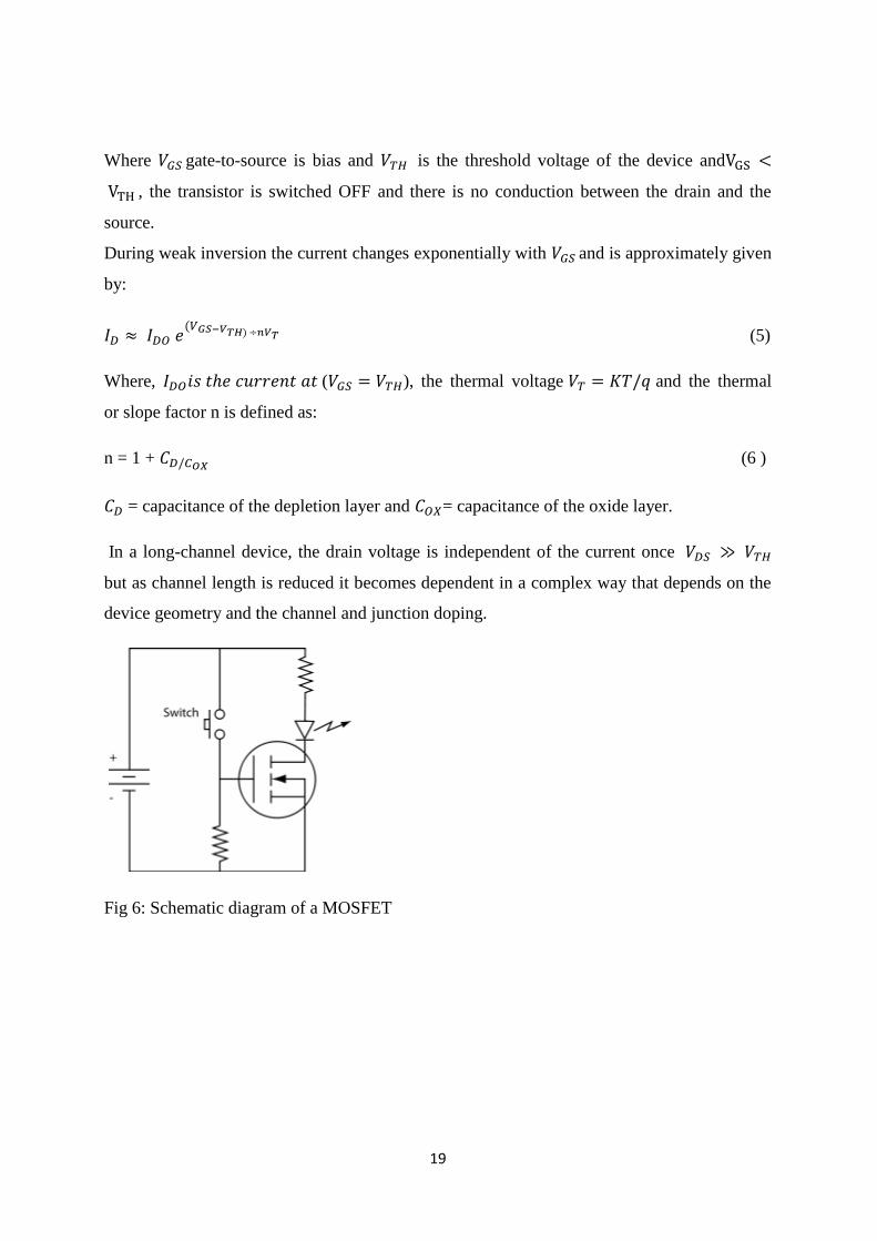
19
Where gate-to-source is bias and is the threshold voltage of the device and
, the transistor is switched OFF and there is no conduction between the drain and the
source.
During weak inversion the current changes exponentially with and is approximately given
by:
(5)
Where, ( ), the thermal voltage and the thermal
or slope factor n is defined as:
n = 1 + (6 )
= capacitance of the depletion layer and = capacitance of the oxide layer.
In a long-channel device, the drain voltage is independent of the current once
but as channel length is reduced it becomes dependent in a complex way that depends on the
device geometry and the channel and junction doping.
Fig 6: Schematic diagram of a MOSFET

20
Fig 7: The graphical relational between the Drain current and drain to source voltage
2.6.1.2 A Triode mode or linear region (also known as the ohmic mode):
When VGS > Vth and VDS < ( VGS – Vth )
In this mode the transistor is turned on, and a channel is created which allows current
to flow between the drain and the source. The MOSFET acts and performs like a resistor
which is controlled by the gate voltage relative to the source and drain voltages. Since the
voltage between transistor gate and source (VGS) exceeds the threshold voltage (VTH), it is
known as Overdrive voltage. The current from drain to source is given as:
)
/2) (7)
Where is the charge-carrier effective mobility, W is the gate width, L is the gate length
and is the gate oxide capacitance per unit area.
2.6.1.3 Saturation or active mode:
When > and (VGS – Vth)

21
The transistor is in ON mode, and a channel is created, which allows current to flow
between the drain and the source. Since the drain voltage is higher than the gate voltage, the
electrons space out, and conduction is through a broader channel now. The onset of this
region is also known as pinch-off and is called so, so as to indicate the lack of channel region
near the drain. The drain current now shows weak dependence on the drain voltage and is
primarily controlled by the gate–source voltage. It is approximately given as:
(8)
(9)
A key design parameter for MOSFETs is the MOSFET output resistance rout given by:
(10)
is the inverse of where, is the expression in saturation region. If λ is taken to be
zero, an infinite output resistance of the device results that leads to unrealistic circuit
predictions, particularly in analog circuits.
2.7 IV CHARACTERISTICS OF SOLAR CELL:
The output characteristics of a solar cell determine the power output that can be
drawn from the cell under varying load demands and changing atmospheric conditions. The
output voltage is a function of the ambient temperature and decreases with an increase in the
temperature due to a reduction in the width of the PN junction. The output current is a
function of the solar insolation as photons are able to knock out more number of electrons.
The output current increases with an increase in the irradiation incident on the surface of the
cell, the temperature being constant.

22
Fig 8: I-V Characteristics at cell temperature of 25°C
2.8 MAXIMUM POWER POINT TRACKING:
The environmental conditions under which a solar power system shall operate can be
broad, as shown in the I-V curves. The current-voltage relationship of a solar array varies
throughout the day, as it changes with respect to environmental conditions such as irradiance and
temperature. In terrestrial applications, Low Irradiance and Low Temperature (LILT) condition
represents the morning condition when the sun just rises. A High Irradiance and High
Temperature (HIHT) condition might reflect a condition near high noon in a humid area. High
Irradiance and Low Temperature (HILT) condition can reflect a condition with healthy sunlight in
the winter. Finally, a condition near sunset can be described by Low Irradiance and High
Temperature (LIHT) condition. For space applications, LILT characterizes a deep space mission
or aphelion period, while HIHT condition is when satellite orbits near the sun (perihelion).

23
Fig 9: I-V characteristics under wide operating conditions
For a uniformly illuminated array, there is only one single point of operation at which
maximum power will be extracted from the array. In a battery charging system where the load
seen by the solar modules is a battery connected directly across the solar array terminals, the
operating point is determined by the battery’s potential. This operating point is generally not the
ideal operating voltage at which the modules are able to produce their maximum available power.
Fig 10: Direct Coupled Method
In the direct coupled method [13], the solar array output power is delivered directly to the loads,
as in figure 10. To match the MPPs of the solar array as closely as possible, it is essential to
choose the solar array I-V characteristic according to the I-V characteristics of the load. A general
idea for the power feedback control is to measure and maximize the power at the load terminal
which assumes that the maximum power of the array equals the maximum load power. However,
the power to the load gets maximized, not the power from the solar array. The direct-coupled
method cannot automatically track the MPPs of the solar array when the temperature or solar

24
radiation changes. The load parameters or solar array parameters must be carefully selected so as
to account for the changes in the solar radiation or temperature.
To be able to extract the maximum power from the solar array and to track the changes due to the
environment, a maximum power point tracking should be implemented. Devices that perform the
requisite function are known as Maximum Power Point Trackers, also called MPPTs or trackers.
A tracker consists of two basic components, as shown in figure 11, a switch-mode converter and a
control with tracking capability. The switch-mode converter forms the core of the entire supply.
The converter allows energy to be drawn at a particular potential, stores it as magnetic energy in
an inductor, and then releases the same at a different potential. Either high-to-low (buck
converter) or low-to-high (boost) voltage converters can be constructed by setting up the switch-
mode section in various topologies. The goal of a switch-mode power supply is to provide a
constant output voltage or current. In power trackers, the whole aim is to provide a fixed input
voltage and/or current, so that the array is kept at the maximum power point, while allowing the
output voltage to match the battery voltage.
Fig 11: Basic components of a maximum power pointer tracker
When properly applied, MPPT control can help to prevent the collapse of the array voltage at very
high load demands, particularly when the supply is to a constant-power type load. One of the
proper approaches is to operate the system in a solar array voltage regulation mode where the
array voltage is clamped to a commanding set point, Vmp, which is dynamically updated by the
MPPT control circuit. The MPPT control processes feedback signals, such as the array current
and voltage, to determine a proper direction in which the operating point is to be moved.
Eventually, this continuously updated set point will fluctuate around the voltage corresponding to
the array peak power point. By adjusting the operating point of the array to the point Vmp, power
output of the array can be maximized, and the most fruitful use of the solar array may be
obtained.

25
For a system without MPPT, the voltage will quickly collapse to zero. This phenomenon can be
understood from the I-V characteristic of a solar array. The flatness of the I-V curve on the left of
the MPP implies that a small incremental increase in current demand leads to large voltage
change. A system with MPPT avoids the voltage collapse by keeping the operating point near the
MPP. On the I-V curve, the operating point corresponding to the maximum-power point is around
the kneel region. Therefore, unlike other power systems with stiff voltage sources, power
conversion from solar arrays with MPPT requires more robust designs due to the inherent risks of
an array voltage collapse under peak load demand or severe changes in the array characteristics.
The location of the MPP of an I-V characteristic is unknown and must be located. A number of
MPPT control algorithms/methods have been proposed. In subsequent sections, these algorithms
will be reviewed.
Fig 12: Typical characteristic curve of a solar cell.
2.8.1 1NCREMENTAL CONDUCTANCE METHOD
In the incremental conductance method, the array terminal voltage is adjusted
according to the MPP voltage it is based on the incremental and instantaneous conductance of
the PV module.

26
Fig 13: Basic idea of incremental conductance method on a P-V Curve of solar
module
The above figure shows that the slope of the P-V array power curve is zero at The MPP, is
positive and increasing to the left of the MPP and negative and decreasing to the right of the
MPP. The basic equations are given as:
𝑑 / 𝑑 = − / - at MPP (11)
𝑑 / 𝑑 > − / - left of MPP (12)
𝑑 /𝑑 < − / - Right of MPP (13)
Where I and V are P-V array output current and voltage respectively. The left hand sides of
the equations represent incremental conductance of P-V module and the right hand sides
represent the instantaneous conductance. When the incremental conductance is equal to the
negative of the instantaneous output conductance, the solar array will operate at the maximum
power point.

27
Fig 14: flowchart of ICM method
2.9 CONCLUSION:
The Photovoltaic cell has been studied here by considering its equivalent circuit
representation. The IV characteristics of the mathematical model of solar cell are studied and the
relationship between the output voltage and output current from the cell is plotted in the graph
using MATLAB-Simulink source. The effect of temperature on IV characteristics of solar cell has
also been studied. With the help of this study and the results, how the concept of Maximum
Power Point Tracking can be used to obtain the maximum power from the solar cell and how to
control the operating point is clearly understood.

28
CHAPTER3
SYSTEM DESCRIPTION

29
3.1 INTRODUCTION:
The cascaded system discussed in this paper has various systems attached to it. It is a
complex system and has various levels of working resulting in the final output we require.
The system uses no transformers but only cascaded inverters which add to the advantages
resulting in higher efficiencies and better cost-effectiveness. The cascaded inverter comprises
of two conventional full-bridge topologies with their AC outputs connected in series. Each
bridge has the capacity to create three different voltage levels at its AC output allowing for an
overall five-level AC output voltage (see Fig 15). One period (20 ms for a 50 Hz signal) can
be divided into six sections, each representing a different operational mode of the inverter.
Fig15: overall system used

30
Fig 16: Example of the cascaded inverter output voltage. The periods I±VI indicate the
different modes the inverter operates in.
3.2 FILTERS:
In order to eliminate the current harmonics around the switching frequency, the grid-
connected inverter for renewable energy source, an output low-pass filter is required. Ideally,
filters that have low cut-off frequency and high attenuation at the high switching frequency do
a much better job at eliminating switching ripples efficiently.
There are 3 types of filters :
1. L FILTER
2. LC FILTER
3. LCL FILTER
3.2.1 L FILTERS:
Firstly, though a single inductor L-filter is quite popular and simple to use, it has low
attenuation and high inductance. The voltage drop across the inductor results in poor system
dynamics, thereby leading to a long-time response. When L-filters are used, the inverter
switching frequency must have a high value in order to sufficiently attenuate the harmonics
[12].

31
Secondly, since lower attenuation of the inverter switching components is achieved by L-
filters, a shunt element is required in order to further attenuate the switching frequency
components. A capacitor is chosen to generate low reactance at the switching frequency and
to produce high magnitude impedance within the control frequency range.
3.2.2 LC FILTERS:
The LC-filter is best suited to such configurations where the load impedance across the
capacitor is relatively high at and above the switching frequency. The capacitance should be
high to reduce cost and losses but a very high value of capacitance is not advisable since
problems such as high reactive current fed on capacitor at the fundamental frequency, inrush
current, possible resonance at the grid side, etc. can occur in the system. If a system is
connected to the grid through an LC-filter, the resonance frequency varies over time as the
inductance value of the grid varies [13].
3.2.3 LCL FILTERS:
In comparison to the previous filter topologies, LCL-filters can provide a better
attenuation at the inverter switching frequency. LCL-filters can produce a better decoupling
between the filter and the grid impedance. LCL-filters are also found to be able to give a good
attenuation ratio even with small C and L values.
However, several constraints have to be considered in designing the three-order LCL-
filter, such as the current ripple through inductors, the resonance phenomenon, the total filter
impedance, the reactive power that the capacitor absorbs, the current harmonics attenuation at
switching frequency etc [14].
3.2.3.1 LCL FILTER DESIGN:

32
The LCL-filter’s equivalent circuit diagram is depicted in Fig.18 and its equivalent
model is shown in Fig.19, where V1 and V2 are inverter and grid voltage respectively, L1, L2,
R1, R2 are the filter inverter-side and grid-side inductor and its equivalent resistors
respectively. A damping resistor R3 is placed in series with capacitor Cf.
Basing on the equivalent circuit diagram of the LCL-filter, the transfer function of LCL
filter using the inverter current as feedback can be derived by assuming that the value of R1
and R2 are quite small so as to be neglected:
G(s) =
(14)
The resonant frequency is √
(15)
Fig 17: Equivalent circuit diagram
Fig 18: Model of LCL Filter
There are some limits on the parameter values while designing such a filter:

33
1.The total per unit inductance should be less than 0.1 because inductances result in the
AC voltage drop during operation. To avoid this, a higher dc-link voltage will be
required which will result in higher switching losses.
2.The capacitance is limited by the reactive power factor (normally this factor is less than
5%).
3.The resonant frequency should be in range:
to avoid resonance
problems, where the utility frequency (rad/s) is, is the resonant frequency
(rad/s) and is the switching frequency (rad/s).
3.3 GRID SYNCHRONISATION:
The number of PV installations has an exponential growth, mainly due to the
governments and utility companies that support programs that focus on grid-connected PV
systems [15], [16].
In a general structure distributed system, the input power is transformed into electricity
by means of a power conversion unit whose configuration is closely related to the input
power nature. The electricity produced can be delivered to the local loads or to the utility
network, depending where the generation system is connected.
One important part of the distributed system is its control.The control tasks can be
divided into two major parts:
1. Input-side controller: Its main property is that it can extract the maximum power from
the input source. Naturally, protection of the input-side converter is also important to
be considered.
2. Grid – side controller: It performs the following:
a. It controls the active power generated
b. It controls the reactive power transfer between the DPGS and the grid
c. Control of the dc-link voltage is done by the grid-side controller
d. It ensures high quality of the injected power

34
The items listed above for the grid-side controller are the basic features this controller should
have. In addition to the above, auxiliary services like voltage harmonic compensation, active
filtering or local voltage and frequency regulation might be requested by the grid operator.
3.3.1 CONTROL STRUCTURES FOR GRID-CONNECTED SYSTEMS:
The control strategy which is applied to the grid-side converter consists primarily of
two cascaded loops. Generally, there is a fast internal current loop, which is responsible for
the regulation of the grid current, and an external voltage loop, which is responsible for the
control of the dc-link voltage [17]-[22]. The current loop takes care of matters related to
power quality and current protection. Hence, harmonic compensation and dynamics are
important properties of the current controller. The dc-link voltage controller is designed so as
to balance the power flow in the system.
The control of grid-side controller is based on a dc-link voltage loop cascaded with an
inner power loop in place of a current loop so that the current injected into the utility network
is controlled indirectly[23].
There are various types of control applications namely :
1.Synchronous Reference Frame Control :
Synchronous reference frame control, also called dq control, uses a reference frame
transformation module, e.g., abc → dq, to transform the grid current and voltage
waveforms into a reference frame that rotates synchronously with the grid voltage. By
such means, the control variables become DC values; thus, filtering and controlling
can be achieved easily. In dq control, the dc-link voltage is controlled in accordance to
the requisite output power. The output is the reference for the active current controller,
whereas the reference for the reactive current is practically set to zero. In the case that
the reactive power is to be controlled, a reactive power reference should be imposed
on the system. The dq control is normally associated with Proportional-Integrals (PI)

35
controller, since they have a satisfactory behavior when regulating dc voltages. The
compensation capability of the low-order harmonics in the case of PI controllers is
very poor, standing as a major drawback when using it in grid connected systems.
2. Stationary Reference Frame Control:
In this case, the grid currents are transformed into stationary reference frame using the
abc → αβ module. Since the control variables are sinusoidal in this situation and due
to the known drawback of PI controller in failing to remove the steady-state error
when sinusoidal waveforms are to be controlled, employment of other controller types
becomes necessary. Proportional resonant (PR) controller [24]-[27] gained a large
popularity in the last decade in current regulation of grid-tied systems.
Characteristic to this controller is the fact that it achieves a very high gain around the
resonance frequency, thus being able to eliminate the steady-state error between the
controlled signal and its reference [26]. The width of the frequency band around the
resonance point depends on the integral time constant Ki. A low Ki leads to a very
narrow band, whereas a high Ki leads to a wider band.
3. Evaluation of Control Structures:
The necessity of voltage feed forward and cross-coupling term is the major drawback
of the control structure implemented in synchronous reference frame. In addition to
that the phase angle of the grid voltage is a must in this implementation. In the case of
control structure implemented in a stationary reference frame, if PR controllers are
used for current regulation, the complexity of the control becomes lower compared to
the structure implemented in dq frame. In addition to that, the phase angle information
is not a necessity, and filtered grid voltages can be used as templates for the reference
current waveform.
In the case of control structure implemented in natural frame, the complexity
of the control can be high if an adaptive band hysteresis controller is used for current
regulation. A simpler control scheme can be achieved by implementing a dead-beat
controller instead. Again, as in the case of stationary frame control, the phase angle
information is not a must. Noticeable for this control structure is the fact that

36
independent control of each phase can be achieved if grid voltages or three single
phase PLLs are used to generate the current reference.
3.4 CURRENT CONTROLLER:
There are various methods to control the current. Controlled current is the inverter
output current , which flows into the low-pass AC filter. Each controller generates a
control signal which contains the information on whether needs to be increased or
decreased. Together with the information on the mode of operation of the inverter, the control
signal is required to derive the switching signals for the individual switches of the inverter.
The PI control method (see Fig. 20) is a common control method in grid- connected PV
systems [28]-[29]. With this control method the frequency of the ripple on is the same as
the frequency of the triangular waveform, which is constant, hence enabling better and easier
AC filter design. However, simulation studies implementing the PI control method for the
cascaded inverter showed that as the mode changes, the control is lost due to non-linear
behavior of the system. The method has therefore not been investigated further for hardware
implementation with the cascaded converter.
Fig 19: PI controller
The hysteresis control (see Fig.21) generates the control signal when exceeding a fixed
magnitude. A disadvantage of this technique is the non-constant frequency in the ripple

37
of , which makes the AC filter design difficult and this method is therefore not
implemented in the hardware of the discussed system.
Fig 20: Hysteresis Controller
The Ramp time Zero Average Current Error (ZACE) control method (see Fig.21) forces the
error of the current to be zero over one switching period. The basic principle of this control
method is indicated in Fig. The controller detects the zero crossings of the current error and
calculates the time until the next switching instant has to occur based on the desired control
signal frequency. The control signal frequency is the same as the frequency of the ripple
current on . The polarity of the current error and the desired control signal frequency are
used to generate the control signal. The frequency of the ripple current is now within a narrow
band. A controller using this method generating PWM frequencies up to 16 kHz has been
realized in practice. The control method can be adapted to the multilevel inverter ensuring
that the control is not lost during changes in the mode.
Fig 21: ZACE controller
3.4 DC VOLTAGE CONTROLLER:
METHOD 1:
DC voltage controller is used to provide the reference current value for the current
controller. It is aimed at keeping the voltage constant on the DC side in normal condition or

38
during grid faults or changes in the input power. The DC link voltage control is changed
according to the balance of power exchanged by the converter.
The DC voltage loop is an outer loop while the current loop is an inner loop. The inner
loop has been designed to achieve a short settling time in order to achieve a fast correction of
the error. The outer loop can be design to be slower. Thus, the inner loop and the outer loop
can be considered as decoupled and thus, they can be linearized.
The DC-link voltage is controlled by means of the converter side DC current and the plant is
given by [30]:
(16)
Where is the switching steady state signal on d-axis which is averaged in the following
computation to a value of 1 and is the value of the DC link capacitor.
The block diagram of the DC link controller is presented in Fig 22:
Fig 22 : Dc voltage loop
In The voltage control loop in S-domain is represented in the figure 22 which also includes
the delay of the current loop and the DC link plant.
The transfer function in continuous domain for the PI controller is given by:
(
) (17)
To obtain the parameters according to this criterion, the phase margin can be imposed at 45°.
Thus the controller parameter can be obtained as follows:
(18)

39
(19)
a = 2.4 (20)
METHOD 2:
Since the primary objective of the controller is to regulate the DC bus voltage within a
narrow band, a PI controller is the obvious choice. It may be noted that the voltage controller
need not be very fast. It is, however desirable, that the transient undershoot or overshoot in
the DC side is limited to a minimum, nominally within 5%. This is achieved by using the DC
side load current as a feed-forward input to the voltage controller. The structure of the
controller, along with the plant, is shown in Figure 23, where KV is the voltage controller
gain, TV is voltage controller time constant, K1 is the gain in the voltage sensing path, and T1
is the time constant.
Fig 23: Modified current control loop
The outer voltage loop is much slower compared to the inner current loop. Hence, the transfer
function of the current control loop has been approximated as:
(21)

40
Fig 24: Voltage control loop.
3.5 CONCLUSION:
The various systems included in the cascaded system are discussed here. The various
control algorithms involved In controlling current and voltage are also discussed. The filter
and grid overview is also given and is found as why they are a necessity in the system.

41
CHAPTER4
SIMULATION RESULTS
42
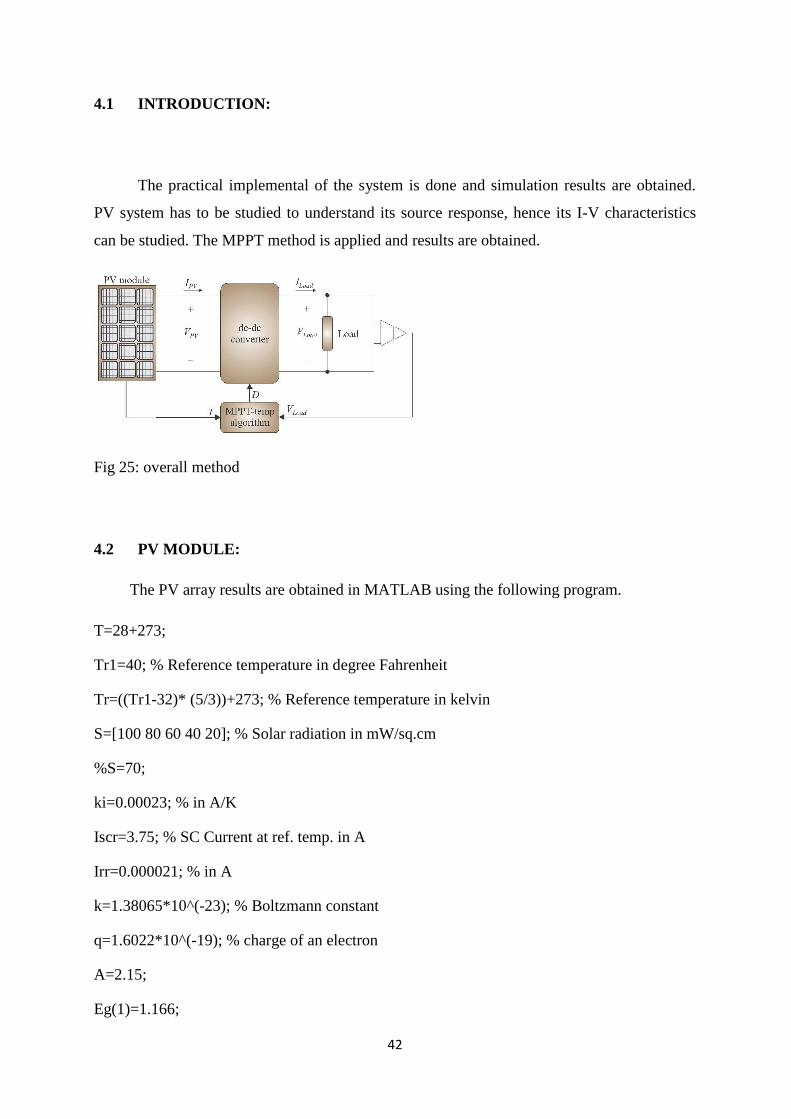
4.1 INTRODUCTION:
The practical implemental of the system is done and simulation results are obtained.
PV system has to be studied to understand its source response, hence its I-V characteristics
can be studied. The MPPT method is applied and results are obtained.
Fig 25: overall method
4.2 PV MODULE:
The PV array results are obtained in MATLAB using the following program.
T=28+273;
Tr1=40; % Reference temperature in degree Fahrenheit
Tr=((Tr1-32)* (5/3))+273; % Reference temperature in kelvin
S=[100 80 60 40 20]; % Solar radiation in mW/sq.cm
%S=70;
ki=0.00023; % in A/K
Iscr=3.75; % SC Current at ref. temp. in A
Irr=0.000021; % in A
k=1.38065*10^(-23); % Boltzmann constant
q=1.6022*10^(-19); % charge of an electron
A=2.15;
Eg(1)=1.166;

43
alpha=0.473;
beta=636;
Eg=Eg(1)-(alpha*T*T)/(T+beta)*q; % band gap energy of semiconductor used
cell in joules
Np=4;
Ns=60;
V0=[0:1:300];
c={'blue','red','yellow','green','black'};
for i=1:5
Iph=(Iscr+ki*(T-Tr))*((S(i))/100);
Irs=Irr*((T/Tr)^3)*exp(q*Eg/(k*A)*((1/Tr)-(1/T)));
I0=Np*Iph-Np*Irs*(exp(q/(k*T*A)*V0./Ns)-1);
P0 = V0.*I0;
figure(1)
plot(V0,I0,c{i});
hleg = legend('100 w/m^2','80 W/m^2','60 W/m^2','40 W/m^2','20 W/m^2');
axis([0 50 0 20]);
xlabel('Voltage in volt');
ylabel('Current in amp');
hold on;
figure(2)
plot(V0,P0,c{i});
hleg = legend('100 w/m^2','80 W/m^2','60 W/m^2','40 W/m^2','20 W/m^2');
axis([0 50 0 400]);

44
xlabel('Voltage in volt');
ylabel('Power in watt');
hold on;
figure(3)
plot(I0,P0,c{i});
hleg = legend('100 w/m^2','80 W/m^2','60 W/m^2','40 W/m^2','20 W/m^2');
axis([0 20 0 400]);
xlabel('Current in amp');
ylabel('Power in watt');
hold on;
end
The I-V curve obtained when the PV array is connected to an open circuit.
Fig 26: I-V curve

45
Fig 27: I-V curve in MATLAB SIMULINK
The P-V curve obtained by the PV array is as below.
Fig 28: P-V curve
PV array output obtained is as follows:
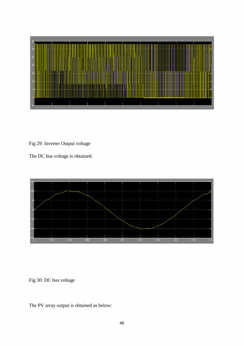
The inverter output voltage is a obtained as given below.
46
Fig 29: Inverter Output voltage
The DC bus voltage is obtained:
Fig 30: DC bus voltage
The PV array output is obtained as below:

47
Fig 31: PV array output
3.3 OVERALL EXPERIMENTAL CIRCUIT:

48
Fig 32: Overall circuit
The PV array block:
Fig 33: PV array block

49
The dc link voltage is obtained in Simulink as below. It should remain constant throughout so
as to obtain the desired voltage level control required by the system.
Fig 34: Dc link voltage
4.4 CONCLUSION:
The PV array results obtained have been verified as per the program and also its
working situations discussed earlier.
0 0.025 0.05 0.075 0.1 0.125 0.15 0.175495
496
497
498
499
500
501
502
503
504
505
Time (in sec)
Vca
pa
cito
r (in
V)

50
CHAPTER5
CONCLUSION AND
FUTURE WORK

51
5.1 CONCLUSION:
The PV array is simulated in the open circuit case and its characteristics are obtained.
The MPPT method used here is found to be more efficient than other MPPT methods and
hence better results are obtained using the incremental conductance method. the simulation
results obtained of the inverter voltage and DC voltage are as per the system design and are
having minimum harmonics.
5.2 FUTURE WORK:
The MPPT method used in this system can be varied with other methods and a better
efficient tracking can be obtained. The various current control methods and dc voltage
controllers used are not of very high efficiency and can be replaced with other types to get a
better result.

52
REFERENCES
[1] Welter P. Power up, prices down, grid connected inverter market survey (Leistung
rauf, Preise runter, MarkituÈ bersicht netzgekoppelter Wechselrichter, in German).
PHOTON-das Solarstrom Magizin (German Solar Electricity Magazine)
1999;3:48±57.
[2] Calais M, Agelidis VG. Multilevel converters for single-phase grid connected
photovoltaic systems Ð an overview. In: Proceedings of the IEEE International
Symposium on Industrial Electronics. Pretoria, South Africa, vol. 1, 1998, p. 224±9.
[3] Martina Calaisa,*, Vassilios G. Agelidisb Michael S. Dymondc, “A cascaded inverter
for transformerless single-phase grid-connected photovoltaic systems, Renewable
Energy, volume 22, Issues 1-3, January – March 2011, page 255-262.
[4] Al-Mohamad, Ali. "Efficiency improvements of photo-voltaic panels using a Sun-
tracking system." Applied Energy 79, no. 3 (2004): 345-354.
[5] Rob W. Andrews, Andrew Pollard, Joshua M. Pearce, “The Effects of Snowfall on
Solar Photovoltaic Performance ”, Solar Energy 92, 8497 (2013).
[6] "Small Photovoltaic Arrays”. Research Institute for Sustainable Energy
(RISE), Murdoch University. Retrieved 5 February 2010.
[7] Reflective Coating Silicon Solar Cells Boosts Absorption Over 96 Percent
Scientificblogging.com (2008-11-03). Retrieved on 2012-04-23.
[8] Solar Cells and their Applications Second Edition, Lewis Fraas, Larry Partain, Wiley,
2010,ISBN 978-0-470-44633-1, Section10.2.
[9] Yuhua Cheng, Chenming Hu (1999). "§2.1 MOSFET classification and
operation". MOSFET modeling & BSIM3 user's guide. Springer. p. 13. ISBN 0-7923-
8575-6
[10] U.A.Bakshi, A.P.Godse (2007). "§8.2 The depletion mode MOSFET" Electronic
Circuits. Technical Publications. pp. 8–2. ISBN 978-81-8431-284-3 Power Electron.,
vol. 9, no.3, pp 676-684.
[11] Hanju Cha and Trung-Kien Vu ,”Comparitive analysis of low pass output filter for
single- phase grid-connected photovoltaic inverter “,Department of Electrical
Engineering, Chungnam National University, Daejon, Korea.
[12] E-Habrouk M., Darwish M.K., Mehta P., "Active power filters: a review", IE
Proceedings-Electric Power Applications, Vol. 147, Iss. 5, pp. 403-413, 2000

53
[13] Akagi H., "Active harmonic filters", Proceedings of the IEEE, Vol. 93, Iss. 12, pp.
2128-2141, 2005
[14] Marco Liserre, Frede Blaabjerg, Steffan Hansen, “Design and Control of an LCL-
Filter-Based Three-Phase Active Rectifier”, IEEE Transactions on Industry
Application, Vol. 41, No. 5, pp. 1281-1291, 2005.
[15] IEA-PVPS, Cumulative Installed PV Power, Oct. 2005. [Online]. Available:
http://www.iea-pvps.org
[16] M. Shahidehpour and F. Schwartz, “Don’t let the sun go down on PV,” IEEE Power
Energy Mag., vol. 2, no. 3, pp. 40–48, May/Jun. 2004.
[17] G. Saccomando and J. Svensson, “Transient operation of grid-connected voltage
source converter under unbalanced voltage conditions,” in Proc. IAS, Chicago, IL,
2001, vol. 4, pp. 2419–2424.
[18] I. Agirman and V. Blasko, “A novel control method of a VSC without ac line voltage
sensors,” IEEE Trans. Ind. Appl., vol. 39, no. 2, pp. 519–524, Mar./Apr. 2003.
[19] R. Teodorescu and F. Blaabjerg, “Flexible control of small wind turbines with grid
failure detection operating in stand-alone or grid-connected mode,” IEEE Trans.
Power Electron., vol. 19, no. 5, pp. 1323–1332,Sep. 2004.
[20] R. Teodorescu, F. Blaabjerg, U. Borup, and M. Liserre, “A new control structure for
grid-connected LCL PV inverters with zero steady-state error and selective harmonic
compensation,” in Proc. IEEE APEC, 2004, vol. 1, pp. 580–586.
[21] S.-H. Song, S.-I. Kang, and N.-K. Hahm, “Implementation and control of grid
connected ac–dc–ac power converter for variable speed wind energy conversion
system,” in Proc. IEEE APEC, 2003, vol. 1, pp. 154–158
[22] H. Zhu, B. Arnet, L. Haines, E. Shaffer, and J.-S. Lai, “Grid synchronization control
without ac voltage sensors,” in Proc. IEEE APEC, 2003,vol. 1, pp. 172–178.
[23] C. Ramos, A. Martins, and A. Carvalho, “Current control in the grid connection of
the double-output induction generator linked to a variable speed wind turbine,” in
Proc. IEEE IECON, 2002, vol. 2, pp. 979–984.
[24] S. Fukuda and T. Yoda, “A novel current-tracking method for active filters based on
a sinusoidal internal model,” IEEE Trans. Ind. Electron., vol. 37, no. 3, pp. 888–895,
2001.
[25] X. Yuan, W. Merk, H. Stemmler, and J. Allmeling, “Stationary-frame generalized
integrators for current control of active power filters with zero steady-state error for

54
current harmonics of concern under unbalanced and distorted operating conditions,”
IEEE Trans. Ind. Appl., vol. 38, no. 2, pp. 523–532, Mar./Apr. 2002.
[26] R. Teodorescu and F. Blaabjerg, “Proportional-resonant controllers. A new breed of
controllers suitable for grid-connected voltage-source converters,” in Proc. OPTIM,
2004, vol. 3, pp. 9–14.
[27] D. Zmood and D. G. Holmes, “Stationary frame current regulation of PWM inverters
with zero steady-state error,” IEEE Trans. Power Electron., vol. 18, no. 3, pp. 814–
822, May 2003.
[28] Keller G, Krieger T, Viotto M. Module oriented photovoltaic inverters: a comparison
of different circuits. In: Conference Record of the 24th IEEE PV Specialists
Conference. vol. 1, 1994, p. 929±32.
[29] Fujimoto H, Kuroki K, Kagotani T, Kidoguchi H. Photovoltaic inverter with a novel
cycloconverter for interconnection to a utility line. In: Conference Record of the 1995
IEEEIndustry Applications 30th IAS Annual Meeting. vol. 3, 1995, p. 2461±7.
[30] M.Liserre, A. Dell’Aquila, F.Blaabjerg “Design and control of a three-phase active
rectifier under non-ideal operating conditions” IEEE Transactions on power
electronics, 2002 Pp: 1181 – 1188


![4607 mp eu-hr barometer_factsheet_nl_]](https://img.dokumen.tips/doc/110x75/58f128ee1a28ab314f8b4593/4607-mp-eu-hr-barometerfactsheetnl.jpg)