Embed Size (px)
Citation preview

A BIDIRECTIONAL UPS INVERTER UTILISING HIGH FREQUENCY 59
Jurnal Teknologi, 40(D) Jun. 2004: 59–76© Universiti Teknologi Malaysia
A BIDIRECTIONAL UPS INVERTER UTILISING HIGHFREQUENCY CENTER-TAPPED TRANSFORMER
ZAINAL SALAM1 & ZULKIFLI RAMLI2
Abstract. A new variation of transformer-isolated inverter for UPS application is proposed. It isbasically similar to the circuit proposed by Koutroulis with the following modifications: 1) a modifiedmodulation technique for the HF PWM inverter stage and 2) replacing the full bridge active rectifierwith a center-tapped active rectifier. With these modifications, the switches count is reduced, andexpectedly, the efficiency is increased. Furthermore, the modified PWM technique will ensure that thetransformer can be utilised near to its full potential. This is due to the absence of the low frequencycomponent that can result in transformer saturation. The paper will detail the design considerations forthe proposed topology. It will primarily focus on the power circuit, modulation method, and the highfrequency transformer design. To prove the concept, a 1-kW prototype inverter was built and tested.
Keywords: Inverter, bidirectional, high frequency transformer, pulse width modulation
1.0 INTRODUCTION
Transformer-isolated inverter is a mandatory requirement for uninterruptible powersupplies (UPS). This is due to the fact that UPS is generally supplied by low voltagebatteries and connected to the utility mains. The main function of the transformer is tostep-up the output voltage to the required mains voltage. The second function is toprovide the required electrical isolation for the inverter.
There has been immense interest on reducing the size of these transformers usingvarious inverter topologies. This is because the transformer represents a substantialportion of the inverter’s weight and cost. Several approaches to reduce the size of thetransformer have been reported in literature over several decades [1–3]. They can bebroadly grouped into two-categories: (1) utilising the ‘line-frequency (50 Hz)’ transformerand (2) using the ‘high-frequency-link’ transformer. Each method presents their ownchallenges and problems, alongside with their tangible benefits.
In this paper, we propose a high efficiency and compact bidirectional HF linkinverter using center-tapped high frequency transformer. With this topology, fewerswitches are used, thus conduction and switching losses are expected to be lower. Inaddition we implement a modified modulation technique for the PWM bridge thatallows for more efficient utilisation of the transformer. The proposed method results insimpler hardware implementation.
1&2Department of Energy Conversion, Faculty of Electrical Engineering, Universiti Teknologi Malaysia,81310 UTM Skudai, Johor, Malaysia. E-mail: [email protected]. Fax: +607-556 6272
JTJUN40D[07].pmd 02/16/2007, 22:2359

ZAINAL SALAM & ZULKIFLI RAMLI60
2.0 TRANSFORMER ISOLATED INVERTER TOPOLOGIES
The line-frequency transformer inverter is shown in Figure 1. It utilises the 50 Hztransformer for isolation and voltage stepped-up/down. This circuit is very attractivedue to its simplicity and ruggedness. It requires minimum number of power switchesand therefore, exhibits low conduction and switching losses. Furthermore, it is inherentlybidirectional, i.e. the power can flow from source to load and vice versa. The reversepower flow is accomplished by the diode which is placed anti-parallel to the mainpower switch.
Despite its simplicity and inherent bidirectional capability, there is one obviousdrawback of this topology which is the 50 Hz transformer. This component is verybulky, and expensive. It constitutes over 60% of the inverter’s weight and space, and asubstantial fraction of the overall cost. Regardless of the PWM modulation methodemployed on the inverter, the size of the transformer remains. It is of great interest toreduce the transformer size, but given the same topology, the task is impossible.
Recently, substantial work is carried out to use high frequency (HF) transformerlink dc/ac inverter as an alternative to the conventional type. Compared to the latter,the HF link inverter offers significant advantages in terms of compactness, weight, andcost. By utilising high frequency transformer, the converter size and weight can bedrastically reduced.
Figure 1 ‘Line-frequency’ inverter
Vdc C
L
50 Hz line-frequencytransformer
vo
Numerous types of bidirectional high frequency link inverters have been suggestedby researchers and are widely publicised elsewhere. However, the two well-knownsurvivors are the ‘cycloconverter’ and the ‘dc-dc converter’ types. The cycloconverterHF link inverter, originally suggested by Matsui [2], is shown in Figure 2. The mainadvantage of this topology is that it requires only two conversion stages, namely theHF square-wave bridge and the cycloconverter circuit. The major disadvantage is thatall the (twelve) power switches operate at high frequency, resulting in appreciableswitching losses. Furthermore, the required switching scheme for the switches in thecycloconverter section is quite complex.
JTJUN40D[07].pmd 02/16/2007, 22:2360

A BIDIRECTIONAL UPS INVERTER UTILISING HIGH FREQUENCY 61
The dc-dc converter type [3] consists of three power stages, i.e. the HF PWM bridge,active rectifier, and polarity-reversing bridge. The circuit configuration is shown inFigure 3. This topology is quite robust and is also capable of bidirectional power flow.However, it appears that the substantial power losses occur due to the forward conductionlosses of the active filter’s diodes. Another drawback of this topology is that the HFPWM bridge requires PWM modulated signal, which makes the transformer designless efficient.
Figure 2 HF link inverter: the ‘cycloconverter’ type
VHF Vo
HF square-wavebridge
Vdc
HFtransformer
Cycloconverter
Figure 3 HF link inverter: the ‘dc-dc converter’ type
VHF Vo
HF PWMbridge
Vdc
HFtransformer
Activerectifier
Polarity-reversingbridge
With regard to transformer capacity utilisation, the dc-dc type is marginally inferiorto the cycloconverter. This is because the former requires PWM modulated signal atthe HF bridge, while the cycloconverter type utilises square wave at 50% duty cycle.Since the PWM output voltage at the transformer primary has different pulse widthsfor each successive pulse, there is a possibility that the transformer may saturate,especially at low modulation index. This is attributed to the fact that a low frequencyenvelope is developed along with the high frequency components. Furthermore, thevariable pulse widths of PWM modulation make the transformer design less efficient.It is difficult to determine the pulse width that is to be used in the design equation aspulses varies continuously over one complete mains cycle.
JTJUN40D[07].pmd 02/16/2007, 22:2361
ZAINAL SALAM & ZULKIFLI RAMLI62
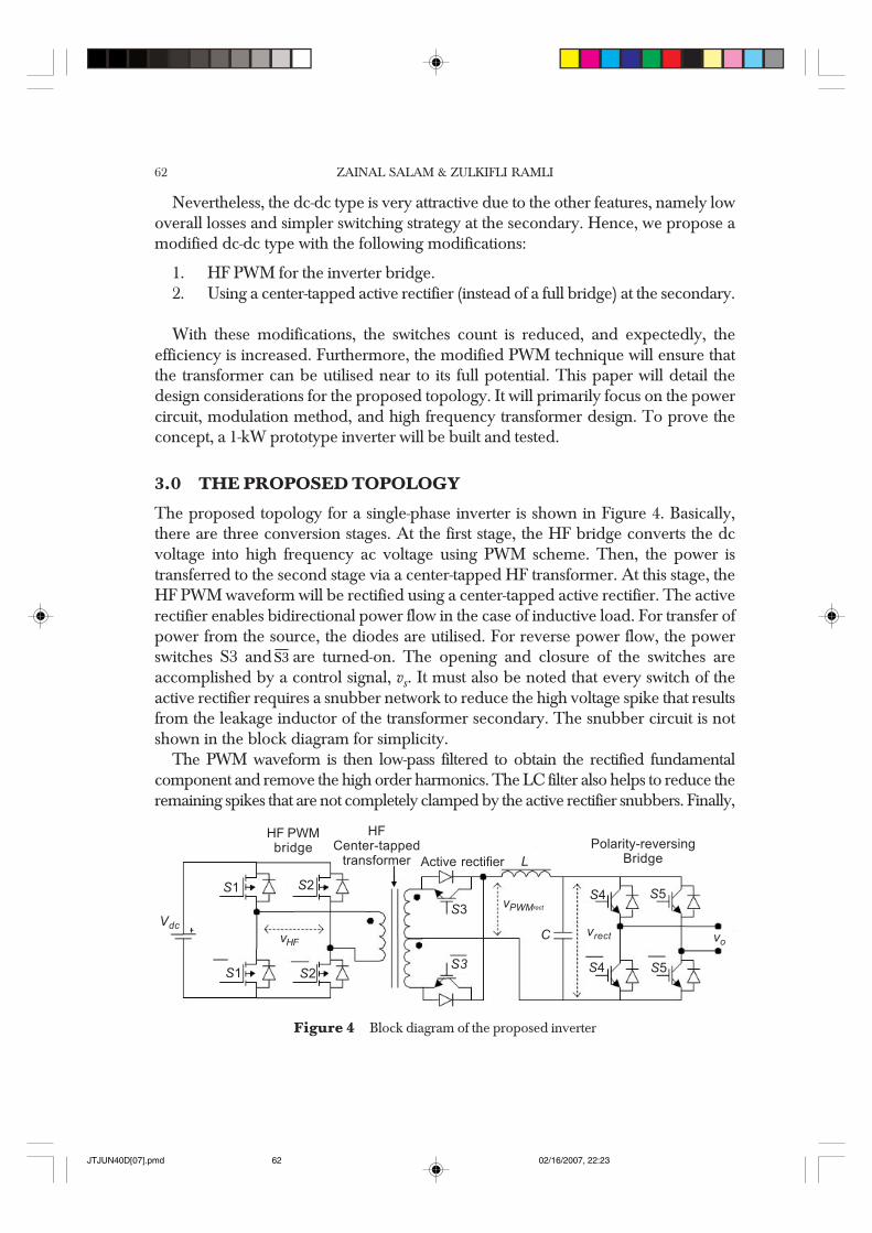
Nevertheless, the dc-dc type is very attractive due to the other features, namely lowoverall losses and simpler switching strategy at the secondary. Hence, we propose amodified dc-dc type with the following modifications:
1. HF PWM for the inverter bridge.2. Using a center-tapped active rectifier (instead of a full bridge) at the secondary.
With these modifications, the switches count is reduced, and expectedly, theefficiency is increased. Furthermore, the modified PWM technique will ensure thatthe transformer can be utilised near to its full potential. This paper will detail thedesign considerations for the proposed topology. It will primarily focus on the powercircuit, modulation method, and high frequency transformer design. To prove theconcept, a 1-kW prototype inverter will be built and tested.
3.0 THE PROPOSED TOPOLOGY
The proposed topology for a single-phase inverter is shown in Figure 4. Basically,there are three conversion stages. At the first stage, the HF bridge converts the dcvoltage into high frequency ac voltage using PWM scheme. Then, the power istransferred to the second stage via a center-tapped HF transformer. At this stage, theHF PWM waveform will be rectified using a center-tapped active rectifier. The activerectifier enables bidirectional power flow in the case of inductive load. For transfer ofpower from the source, the diodes are utilised. For reverse power flow, the powerswitches S3 and S3 are turned-on. The opening and closure of the switches areaccomplished by a control signal, vs. It must also be noted that every switch of theactive rectifier requires a snubber network to reduce the high voltage spike that resultsfrom the leakage inductor of the transformer secondary. The snubber circuit is notshown in the block diagram for simplicity.
The PWM waveform is then low-pass filtered to obtain the rectified fundamentalcomponent and remove the high order harmonics. The LC filter also helps to reduce theremaining spikes that are not completely clamped by the active rectifier snubbers. Finally,
Figure 4 Block diagram of the proposed inverter
S4
vrect
vPWMrect
vHF
Vdc
S3
S3
S2S1
S2S1
L
vo
S5
S4 S5
Polarity-reversingBridgeActive rectifier
HF PWMbridge
HFCenter-tapped
transformer
C
JTJUN40D[07].pmd 02/16/2007, 22:2362
A BIDIRECTIONAL UPS INVERTER UTILISING HIGH FREQUENCY 63
using a polarity-reversing bridge, the second half of the rectified sinusoidal voltage waveformis inverted at zero-crossing, and the sinusoidal output waveform is obtained. Note that thepolarity-reversing bridge utilises only supply switching frequency switches.
Using this configuration, the total number of power switches is reduced into ten.From this, only six switches are switched at high frequency.
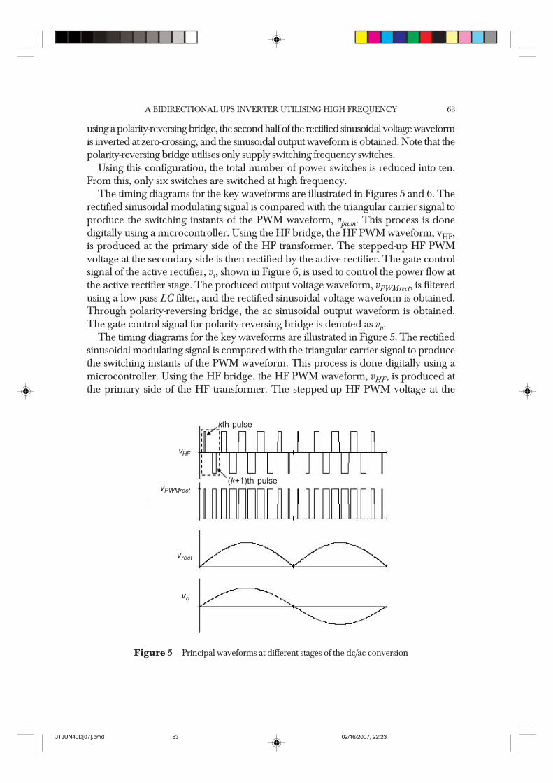
The timing diagrams for the key waveforms are illustrated in Figures 5 and 6. Therectified sinusoidal modulating signal is compared with the triangular carrier signal toproduce the switching instants of the PWM waveform, vpwm. This process is donedigitally using a microcontroller. Using the HF bridge, the HF PWM waveform, vHF,is produced at the primary side of the HF transformer. The stepped-up HF PWMvoltage at the secondary side is then rectified by the active rectifier. The gate controlsignal of the active rectifier, vs, shown in Figure 6, is used to control the power flow atthe active rectifier stage. The produced output voltage waveform, vPWMrect, is filteredusing a low pass LC filter, and the rectified sinusoidal voltage waveform is obtained.Through polarity-reversing bridge, the ac sinusoidal output waveform is obtained.The gate control signal for polarity-reversing bridge is denoted as vu.
The timing diagrams for the key waveforms are illustrated in Figure 5. The rectifiedsinusoidal modulating signal is compared with the triangular carrier signal to producethe switching instants of the PWM waveform. This process is done digitally using amicrocontroller. Using the HF bridge, the HF PWM waveform, vHF, is produced atthe primary side of the HF transformer. The stepped-up HF PWM voltage at the
Figure 5 Principal waveforms at different stages of the dc/ac conversion
kth pulse
vHF
vPWMrect
vrect
vo
(k+1)th pulse
JTJUN40D[07].pmd 02/16/2007, 22:2363

ZAINAL SALAM & ZULKIFLI RAMLI64
Figure 6 Modulating technique and signal generated by microcontroller
vpwm
Modulating signal
vs
vu
Carrier signal
secondary side is then rectified by the active rectifier. The gate control signal of theactive rectifier, vs, shown in Figure 6, is used to control the power flow at the activefilter stage. The produced output voltage waveform, vPWMrect, is filtered using a lowpass LC filter, and the rectified sinusoidal voltage waveform is obtained. Throughpolarity-reversing bridge, the second half of the rectified sinusoidal voltage waveformis inverted at zero-crossing, thus producing the ac sinusoidal output waveform. Thegate control signal for polarity-reversing bridge is denoted as vu.
4.0 MODULATION METHOD
In this work, the modulation technique of the HF bridge is based on the symmetricregular sampling sinusoidal PWM. The derivation of the switching angles isaccomplished using the volt-second equalization method, as illustrated in Figure 7.The PWM pulse width characterization is also shown in the same figure. Note that themodulating waveform is a rectified sinusoidal signal. The equation used to calculatethe pulse width of the kth PWM for a given modulation index, MI, and modulationratio, mf, is given as follows:
δk = 4δo MI sin αk (1)
where
=
12fm
k
Using Equation (1), the rising and falling edges (i.e. the switching instants) of thekth pulse can be known. For the rising edge, the angle can be calculated as:
α1k = αk – δk (2)
JTJUN40D[07].pmd 02/16/2007, 22:2364

A BIDIRECTIONAL UPS INVERTER UTILISING HIGH FREQUENCY 65
For the falling edge,
α2k = αk + δk (3)
Looking back into Figure 5, it can be noticed that the widths for kth and (k+1)thpulses are not equal in vHF. If the differences in the pulse widths are plotted from k=1through mf, it can be observed that a low frequency voltage envelope existed alongwith the high frequency component. This may results in transformer saturation, as thetransformer is normally designed for high frequency operation. Alternatively, thetransformer can be utilized below its rated capacity to avoid the possible saturation.
To overcome this problem, we propose the kth pulse width to be equalized to the(k+1)th. Using this approach, the use of dc blocking capacitance at primary side oftransformer, as suggested in [3] can be avoided. Furthermore, the processing speed tocalculate the pulse widths can be increased, with only mf /8 pulses to be calculated ineach cycle. The following equation is used for this purpose:
δk = δ(k+1) = 4δoMI sin (αk′) (4)where:
+ +′ = = −
1 1 3 5 12 2
fk kk
m, k , ,
α αα
Figure 7 Volt-second modulation technique
0
0
x
x
δo δo δo δo
+Vdc
0
0
δkδk
α1k α2k
αk
JTJUN40D[07].pmd 02/16/2007, 22:2365

ZAINAL SALAM & ZULKIFLI RAMLI66
5.0 HARDWARE DESIGN
5.1 PWM Waveform Generation
The Siemen’s C167 microcontroller has been chosen as the waveform generator forthe PWM and other control signals in the circuit. It is a low cost, 16-bit fixed-pointmicrocontroller, equipped with extensive on-chip peripherals to assist interfacing withother external components. Some of these peripherals are independent modules thatrequire minimum intervention from the main CPU, thus freeing the latter to performother tasks.
The PWM waveform generation is accomplished by the C1676 peripheral knownas the PWM Module. Four PWM channels are available , which can be programmedseparately for different types of PWM modes. In this work, the center aligned PWMmode, shown in Figure 8 has been selected as the gate signal for the HF bridge. ThePWM signals generated by the microcontroller will then go through a series of externallogic gates and become the input signals of gate drivers as shown in Figure 9.
5.2 Power and Driver Circuit
The HF bridge is constructed using the IRFP460 power MOSFET. It is a low Rds(ON)device with good switching capability. The active rectifier’s switch is built using theIRG4PH40K IGBTs with discrete 20EFT10 fast recovery anti-parallel diodes. The rated
Figure 8 Center-aligned PWM mode using the C167 PWM module
PPxPariod=7
PTxCount value
PWx PulseWith=0
PWx=1
PWx=2
PWx=4
PWx=5
PWx=7
PWx=8
LSRLatch shadow
RegisteredInterruptRequest
Change countdirection
LSR
87.5%
75%
50%
25%
12.5%
0%
100%
Duty cycle
MCAD1950
JTJUN40D[07].pmd 02/16/2007, 22:2466

A BIDIRECTIONAL UPS INVERTER UTILISING HIGH FREQUENCY 67
voltage for the diode is 1200V, in precaution to the possible voltage surge that mayresult from the transformer leakage inductance. An RC snubber network has beenplaced across the active rectifier’s switch to reduce the surge voltage. The polarity-reversing bridge is constructed using SK25GB065 IGBT module. Since almost all thesurge voltages have been filtered before entering polarity-reversing bridge, the chosenpower switches are only rated at 600 V. Using low voltage IGBT, the forward conductionlosses can be minimized.
Each power transistor is driven by a Hewlett Packard gate driver chip, HCPL 3120.This chip has a built-in opto-coupler, mid-stage amplifier, and output-stage (power)amplifier. The ‘all-in-one chip’ solution has simplified the gate-driver to power transistorinterface greatly. To obtain the isolated power supplies for the top and bottom gate-driver of an inverter leg, a transformer-isolated DC-DC converter is designed. Theheart of the DC-DC converter is the SG3524 pulse generator, while the isolation isperformed by the ET12 Ferroxcube high frequency miniature transformer. Using asingle 9 V battery, all the gate-drivers are isolated and are individually powered to +15Volts (to turn on the switch) and –15 V (to turn off).
A dead-time compensation scheme for the HF bridge is incorporated into thesoftware. The waveform for the compensation is shown in Figure 10. Note that td is theamount of dead-time taken away from the pulse width.
5.3 Power Transformer Design
As has been emphasised throughout the discussion, the main feature of the highfrequency link inverter is transformer size reduction. To achieve this goal, typically
Figure 9 Interface between the microcontroller with the power switches
Gate drive
Gate drive
vpwm
Mic
roco
ntr
olle
r
Gate drive
Gate drive
Gate drive
Gate drive
Gate drive
Gate drive
vu
vs
S1
S1
S2
S3
S4
S5
S5
S4
S3
S2
Gate drive
Gate drive
JTJUN40D[07].pmd 02/16/2007, 22:2467

ZAINAL SALAM & ZULKIFLI RAMLI68
ferrite cores are selected due to its low core loss when operated at high frequency.Ferrite core has a simple structure, good winding coupling, and easy to construct. It isalso significantly lower in cost.
The procedure of designing a transformer inevitably started by choosing the size ofthe core. This mainly depends on the power capacity required for the transformer.The relationship between the power capacity (Po) and the effective core area, Ae, andcore windows area, Ac, at a given switching frequency (f ) is given as [4].
23 39(10 ) cmae c o
max
. DA A P
B f
=
(5)
and2sat
maxB
B ≅ (6)
Where Bsat and Dcma is the saturation flux density and diameter in circular mils,respectively. Subsequently, the number of primary winding, Np can be determinedby:
510
4p
pmax e
V DN
B A f= (7)
Figure 10 Dead-time compensation scheme for the HF bridge
Ideal pulse Ideal pulse
δktd
td
δkνpwm
νHF
νpwm rect
S1
S1
S2
S2
δk – tdδk
(a) Before compensation
Added pulse with
(b) After compensation
Lost pulse width
JTJUN40D[07].pmd 02/16/2007, 22:2468

A BIDIRECTIONAL UPS INVERTER UTILISING HIGH FREQUENCY 69
In equation (7), D is the duty ratio, which varies from 0 to 0.5. The secondary turnsratio can be calculated as:
ss p
p
NV V
Nη= (8)
Vs and Vp are the primary and secondary voltage, respectively, while η is the assumedefficiency of the transformer. Design example of the transformer used in this work isattached in Appendix A.
The designed high frequency transformer with power rating of 1000 VA has anapproximate size of 2.5 in × 2.5 in and weighted 500 g. For comparison, a 50 Hz line-frequency transformer of the same rating is 6 in × 6 in and has a weight of approximately7 kg. Figure 11 shows the finished prototype inverter. The total weight of the inverter isabout 1.4 kg. Apart from the power transformer and inductor, substantial portion ofthe weight is contributed by the heat sink and cooling fan.
Figure 11 Photograph of the prototype inverter
Low pass filter
Microprocess module
Power circuit
HF center-tapped transfomer
Gate drive module
6.0 EXPERIMENTAL RESULTS AND DISCUSSIONS
Laboratory experiments have been carried out to verify the viability of the proposedinverter. The specifications of the inverter are as follows:
• Input voltage ranged from 60 to 110 V.
• Sinusoidal output voltage 220-250 Vrms, 50 Hz.
• Maximum output power of 1 kW.
The output waveforms for resistive load and inductive load are shown in Figure 12and Figure 13 respectively. From the latter, it can be observed that the inverter is
JTJUN40D[07].pmd 02/16/2007, 22:2469

ZAINAL SALAM & ZULKIFLI RAMLI70
capable of carrying bidirectional power flow. To measure the harmonics of the inverteroutput, the LC filter is disconnected. The frequency spectrum is shown in Figure 14.The main harmonic components exist at and around the multiples of switchingfrequency, which are mf, 2mf, 3mf, and 4mf. This is to be expected because themodulation technique is basically based on sinusoidal PWM.
Figure 12 Output voltage and current with resistive loadoutput power = 1050WScales: output voltage 100 V/div, output current 4 A/div,time 5 ms/div
Io(t)
Vo(t)
SampleTak Rum: 50.0 kS/s
Figure 13 Output voltage and current with inductiveload. Real power = 511.7 W; power factor = 0.7Scales: output voltage 100 V/div, output current 2 A/div,time 5 ms/div
102011Tak Rum: 50.1 kS/s
Io(t)
Vo(t)
JTJUN40D[07].pmd 02/16/2007, 22:2470
A BIDIRECTIONAL UPS INVERTER UTILISING HIGH FREQUENCY 71
Figure 14 Frequency spectrum of the output voltage withoutLC filter. Parameters: MI = 1.0, mf = 650Scales: spectra 40 V/div, frequency 12.5 kHz/div
1.0 Vo(t)
SampleTak Rum: 3 kS/s
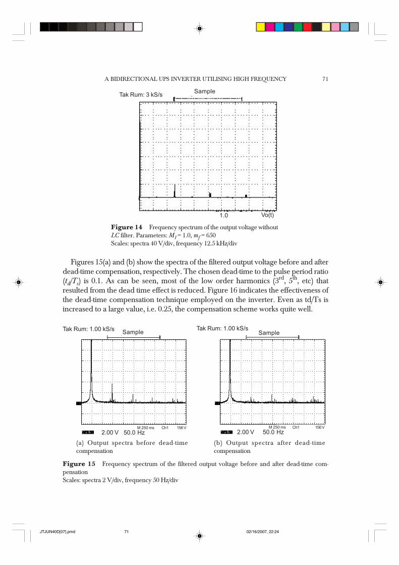
Figures 15(a) and (b) show the spectra of the filtered output voltage before and afterdead-time compensation, respectively. The chosen dead-time to the pulse period ratio(td/Ts) is 0.1. As can be seen, most of the low order harmonics (3rd, 5th, etc) thatresulted from the dead time effect is reduced. Figure 16 indicates the effectiveness ofthe dead-time compensation technique employed on the inverter. Even as td/Ts isincreased to a large value, i.e. 0.25, the compensation scheme works quite well.
(a) Output spectra before dead-timecompensation
SampleTak Rum: 1.00 kS/s
2.00 V 50.0 Hz
Figure 15 Frequency spectrum of the filtered output voltage before and after dead-time com-pensationScales: spectra 2 V/div, frequency 50 Hz/div
(b) Output spectra after dead-timecompensation
SampleTak Rum: 1.00 kS/s
2.00 V 50.0 HzM 250 ms Ch1 156 VM 250 ms Ch1 156 V
JTJUN40D[07].pmd 02/16/2007, 22:2471

ZAINAL SALAM & ZULKIFLI RAMLI72
The measured output voltage THD for resistive load is shown in Figure 17. It canbe seen that the output voltage THD is less than 1% over the entire output power, withthe average value approximately 0.5%. This can be attributed to the effectiveness of thedead-time compensation scheme. The measured values are much less than the 5%level, the industrial standard for UPS systems. The minimum value of THD (0.35%) isobtained when the inverter operates at output power 600 – 700 W.
Figure 16 Effectiveness of the dead-time compensationfor various values of td /Ts
02468101214161820
0.05 0.10 0.15 0.20 0.25td /Ts
% T
HD
Without dead-time compensation
With dead-time compensation
Figure 17 Output voltage THD versus output power
TH
D (
%)
Output power (W)
JTJUN40D[07].pmd 02/16/2007, 22:2472

A BIDIRECTIONAL UPS INVERTER UTILISING HIGH FREQUENCY 73
Figure 18 Efficiency vs output power of the inverter
80
82
84
86
88
90
92
94
96
98
00
HF bridge inverter
Output power (W)
Eff
icie
ncy (
%)
100
80
82
84
86
88
90
92
94
96
98
HF link inverter
HF transformer
Figure 18 shows the measured efficiency of the inverter at each conversion stages,against the output power. The average efficiency of HF bridge is 95%, while the meanefficiency of the HF transformer is 91%. The average total efficiency of the inverter isaround 88%. Note that when the output power increases to 1 kW, the average efficiencydecreases to the minimum level of 87%. This can be attributed to the increased lossesof power switches and transformer at high current operation.
7.0 CONCLUSION
A compact HF link inverter that enables bidirectional power flow using center-tappedtransformer has been described. The use of center-tapped active rectifier requires lesspower switches, thus increases the overall system efficiency. The modified digitalPWM technique allows better utilisation of the transformer capacity. It also increasesthe switching angle calculation processing speed. A 1kW prototype is constructed tostudy the viability of the inverter. It was found that the output voltage has a very lowTHD with an average efficiency of 88%.
ACKNOWLEDGEMENTS
The authors wish to acknowledge the Ministry of Science, Technology and theEnvironmental (MOSTE), Malaysia, for the financial funding of this project.
300 500 600 700 800 900 1000400
JTJUN40D[07].pmd 02/16/2007, 22:2473

ZAINAL SALAM & ZULKIFLI RAMLI74
REFERENCES[1] Bowes S. R. 1975. New Sinusoidal Pulse Witdh Modulated Inverter. Proceedings of the IEEE. 122(11): 101-
105.[2] Matsui, M., M. Nagai, M. Mochizuki., and A. Nabae. 1996. High-frequency link dc/ac converter with
suppressed voltage clamp circuits-Naturally commutated phase angle control with self turn-off devices. IEETrans. on IA. IA-32(2).
[3] Koutroulis, E., and J. Chatzakis. 2001. A bidirectional, sinusoidal, high-frequency inverter design. IEE Proc-Electric Power App. 148(4).
[4] Billings, K. H. 1989. Handbook of Switch mode Power Supply. Mc Graw-Hill Publishing Company.
APPENDIX A
Transformer Design Example
In this work, the designed high frequency transformer has to meet the followingspecifications:
• input voltage range, Vmax = 67.5 V – 100 V.
• switching frequency, f = 17 kHz.
• maximum input power, = 1000 W.
The design procedure of the transformer are summarised as follows:
1. Selection of core geometry and core material.For the power and frequency ratings, an EE geometry with ferrite grade material3C90 from Ferroxcube is selected.
2. Selection of flux density, Bmax.Information from data sheets show that ferrite with grade 3C90 has the saturatedflux density, Bsat of 3500 Gauss at 100C. Thus,
35001700
2 2sat
maxB
B G≅ = =
3. Determination of conductor size.Calculated current density is 500 ampere per circular mils. Thus the required sizeof conductor would be 7120 circular mil. The most appropriate diameter for aconductor to operate at frequency of 17 kHz is approximately 1.06 mm, takinginto account the conductor skin effect. Alternatively, five conductors sized awg-18 (in parallel) can be used to obtain the equivalent area of a conductor sizedawg-12.
JTJUN40D[07].pmd 02/16/2007, 22:2474

A BIDIRECTIONAL UPS INVERTER UTILISING HIGH FREQUENCY 75
4. Determination of core and bobbin size.To calculate the core dimension, Equation (5) is used. The selected core shouldhave a greater size than the calculated value to ensure that all winding fitted wellinto the core. Hence:
2 24
3
3 39(10 ) 3 39(10 )500(1000 ) 5 87cm
170 10 (17 10 Hz)cma
e c omax
. D .A A P W .
B f G
= = =
× ×
Core and bobbin 3C90 ETD54 have been chosen with AeAc value of 8.848 cm4.
5. Calculation of the primary turns:Using Equation (8), the secondary turns can be estimated as:
= = =55
2
10 (66.7 V)(0 5)1020 6 turn
2 2(1700 )(2 8 cm )(17 kHz)dc
pmax e
.V DN .
B A f G .
6. Calculation for Secondary turns:Calculation is done using Equation (11). However, the voltage drop of the powerswitch and certain circuit parameters should be taken into consideration. Theseinclude:
• The IGBT saturated voltage: Vce = 1.8 V;
• MOSFET voltage drop: Ids × Rds = 14.24 A × 0.085;
• Diode forward biased voltage: VF = 1.2 V;
• Estimated transformer’s efficiency: η = 80%;
• The minimum modulation index, p = 0.7;
Using these values, the minimum input voltage of primary winding can beestimated as:
Vp = Vmin – 2(IdsRds) = 67.5 – 2(14.24 × 0.085 Ω) = 65.1 V
The output sine wave voltage,
Vout = 240 + Vd + Vce = 240 + 2 × 1.8 V + 1.8 V = 245.4 V
Hence the secondary voltage is:
2 245 4 2495 8 496 V
0 7out
sV .
V .p .
×= = = ≅
The secondary turns can be calculated as:
0 8 496 V 21128 winding
65 1s p
sp
V N .N
V .
η × ×= = =
JTJUN40D[07].pmd 02/16/2007, 22:2475

FURTHER READING
Click any one of the following links to be taken to a website which contains the following documents.
There appears to be a lot of recent patent activity in the areaof building "bridgeless PFC convertors". The following aresome of the patents.
11_584_983_Method_and_apparatus_for_high_efficieny_rectifier11_204_307_AC_to_DC_power_supply_with_PF11_302_544_Simple_partial_switching_power_factor_correction11_474_712_BRIDGELESS_BI_DIRECTIONAL_FORWARD_TYPE_CONVERTER11_480_004_High_efficiency_power_converter_system11_706_645_AC_to_DC_voltage_converter_as_power_supply12_401_983_BRIDGELESS_PFC_CIRCUIT_FOR_CRM12_798_682_Bridgeless_PFC_converter
3295043_MASSEY_D_C__TO_D_C__REGULATED_CONVERTER4183079_DC_AC_inverter4523266_AC_to_DC_conversion_system4943902_AC_to_DC_power_converter_and_method5570276_Switching_converter_with_open_loop_input_regulation5815380_Switching_converter_with_open_loop_Primary_regulation5815384_Transformer_uses_bi_directional_synch_Rectifiers6115267_AC_DC_converter_with_no_input_rectifiers6157182_DC_DC_converter_with_multiple_operating_modes6608522_DC_to_DC_converter_providing_stable_operation7250742_Digital_control_of_bridgeless_power_factor_correction7265591_CMOS_driver_with_minimum_shoot_through
And here is some more information for those who may be interested.
A BIDIRECTIONAL PWM THREE-PHASE STEP-DOWN RECTIFIERA bidirectional, sinusoidal, high-frequency inverterA DUAL INPUT BIDIRECTIONAL POWER CONVERTERA new structure for bidirectional Power flowBI-DIRECTIONAL INVERTER-CHARGER Bi-directional single-phase half-bridge rectifier for power qualityBiDirectional ConverterBidirectional_UP_InverterSynthesis of Input-Rectifierless AC/DC
11.28.10_10.11AM [email protected] Sauer http://www.idea2ic.com/