Embed Size (px)
Citation preview

A 400 to 500-MHz CMOS Power Amplifier with Multi-Watt Output
Jeongmin Jeon, Student Member, IEEE and William B. Kuhn, Senior Member, IEEE
Kansas State University, Manhattan, KS, 66502, U.S.A.
Abstract –- A two-stage P-band (400 MHz) CMOS multi-Watt Power Amplifier (PA) is reported. Four identical 1.25-Watt PA cells are power-combined to generate approximately 5-Watt output. The same PA chip is used for a drive-amplifier, providing a total of 17 dB power gain.
In the measurements, the two-stage five-chip PA produces 5.1-Watt with 17 % PAE. The five-chip PA assembly will be merged into a 7×10 mm2 single die amplifier in a future project.
Index terms –- CMOS, UHF, PA, power amplifier
I. INTRODUCTION
Although compound materials, such as GaAs and GaN, and specially processed LDMOS are preferred over CMOS in commercial RF power amplifiers (PA) [1], Watt-level CMOS PA has been intensively researched for decades. As many components of radio are realized by CMOS analog/digital circuits, the CMOS PA is needed to be integrated to achieve a single chip radio.
Watt-level PAs in cellular bands utilize off-chip components or bondwires in the absence of high Q inductor/balun [2] [3] [4] [5]. Utilizing a DAT (distributed active transformer) technique, fully integrated PAs have been also reported in 900 MHz and 2.4 GHz by Han and Aoki, respectively [6] [7]. Notably, the Aoki’s PA reported the highest output power, 2-Watt, by a CMOS PA. Since the DAT technique is not scalable due to limited 3×3 mm2 die size at P-band (400 MHz), instead, the authors demonstrated a fully integrated CMOS 1-Watt PA with high-Q 1:3 turns-ratio output balun [8]. However, if the die size is large enough, the DAT technique is still viable for higher output power at P-band.
In this paper, we present a 3 to 5-Watt CMOS power amplifier implemented in Silicon On Sapphire (SOS) and operating at P-band (400 MHz) by DAT power-combining. The design is intended for use in a phased array radar where high levels of integration are needed to decrease mass, and where the cost is justified by the integration goals. Although currently implemented by wirebonding multiple dies on a PCB level, the layout allows for full integration in future projects.
II. BACKGROUND AND DESIGM METHODS
In order to produce 5-Watt output power, the PA design leverages an existing 1-Watt PA circuit developed previously by the authors [8]. The 1-Watt PA was capable of 30 dBm output with 27 % PAE when operating with 50 Ohm single-ended inputs and outputs. The 5-Watt extrapolation was created by reworking the I/O circuits (transformers) to provide 12.5 Ohm secondaries, each with 1.25-W output, that are power combined as shown in the schematics of Figure 1. A parallel capacitor of 25pF is used to resonate out leakage inductance in the inter-stage matching.
Hence, only a single 1.25-Watt design is required for the prototype – limiting fabrication cost. Four copies of this die are connected with bondwires to form the 5-Watt output-
Figure 1. A two-stage five-chip configuration employing power-combining
Figure 2. Schematics of a single PA chip
978-1-4244-2699-7/09/$25.00 ©2009 IEEE 273 RWS 2009
TU2P-10
978-1-4244-2699-7/09/$25.00 ©2009 IEEE 272 RWS 2009
stage design in the current implementation. A fifth copy is used as a drive-amplifier.
As shown in Figure 2, the PA unit utilizes stacked PMOS transistors for high breakdown voltage and high-Q on-chip baluns/transformers at input and output, following the design methodology in the 1-Watt PA [8]. In conjunction with the 1:1 balun, output network is tuned for a class-E/Fodd [9]. Utilizing insulating substrate, Qs of the output balun are 16 and 15 at the primary and the secondary, respectively. C1 and C2 are added for the optimum efficiency. C3 and bondwires are used at the gates of M3 and M4 for ac and DC ground. The layout of the core tile is shown in Figure 5a, and the full five-tile set is shown in Figure 5b. The size of the core tile is 3.3 × 3.3 mm2.
It is important to note that the layout was done to allow a fully-integrated 5-Watt PA to be developed from the same design in later fabrications. The design employs five copies of a core 1.25 Watt tiles with bondwire interconnects only to save prototyping cost.
III. SIMULATED AND MEASURED RESULTS
The circuit in Figure 1 was simulated in Agilent ADS and
the results are shown in Figure 3 and 4. The PA generates 36.6 dBm (4.6-Watt) output power with PAE of 37 % at 400 MHz, using 20 dBm input power. 80 MHz 1-dB bandwidth and 180 MHz 3-dB bandwidths are obtained.
Figure 5 shows pictures of the fabricated die bondwire-connected on a PCB. The chip on the left hand side in Figure 5b drives the four-chip output-stage on the right hand side in the same picture. Capacitors between the stages are small-valued and can be integrated with ease when a 7×10 mm2 die is granted for the whole PA integration. Figure 5a shows a closeup of the single tile.
(a)
(b)
Figure 5: Photo of (a) the PA unit (b) the five-chip PA assembly
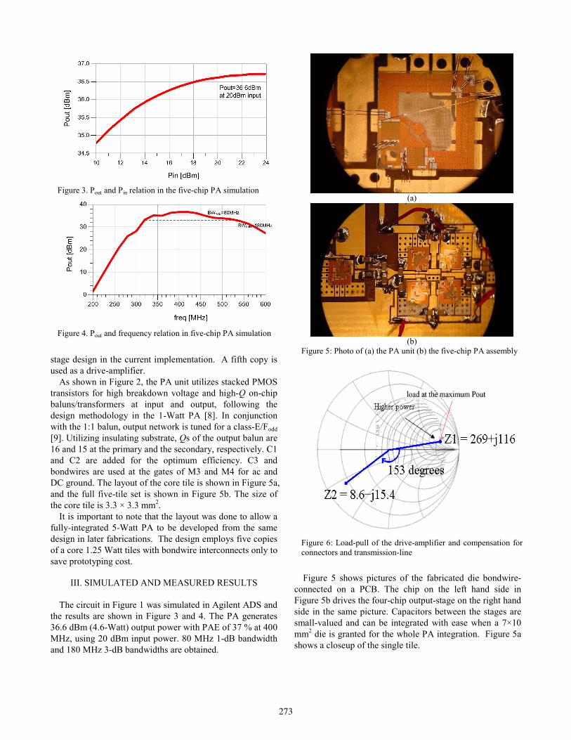
Figure 6: Load-pull of the drive-amplifier and compensation for connectors and transmission-line
Figure 3. Pout and Pin relation in the five-chip PA simulation
Figure 4. Pout and frequency relation in five-chip PA simulation
274273

Prior to building up the full five-chip PA, the drive-stage
and the output-stage were tested separately. In load-pull test of the drive-amplifier, the PA generated 28.8 dBm output power at Z1 = 269 + j116 Ohms as shown in Figure 6. The plot can be misleading since the output power increases as magnitude of the load increases. However, when an electric length of connectors and transmission-line between a tuner and the PA, equivalent to 153º phase rotation, is compensated, the load impedance at the edge of the drive-PA chip Z2 is 8.5 − j15.4 for the maximum power, which is close to the initial design assumption, 12.5-Ohm driving.
Secondly, the four-chip output-stage was tested with an external power amplifier and 4.5 V power supply. The external input is set at 28 dBm and the PA generates 4.3-Watt at 520 MHz with 19 % drain efficiency and 17 % PAE. Gain of the PA is 8.4 dB. When Pin is 30 dBm, Pout is 5.1-Watt as shown in Figure 7a with 21 % drain efficiency and 17 % PAE. Figure 7b shows that its 1dB BW is greater than 20 %. The 120 MHz frequency offset from the intended 400MHz center frequency is caused by a layout mistake, but
(a)
(b)
Figure 8: Measured performance of the two-stage five-chip PA including the drive-amp. (a) Output power and PAE. (b) Frequency sweep.
(a)
(b)
(c)
Figure 7: Measured performance of the output stage when it is driven by the external PA. (a) Output power and PAE. (b) Frequency sweep. (c) Power supply sweep.
275274

the reason of two dips at 450 MHz and 550 MHz are not known. It is possible that they will disappear once the frequency offset is corrected. However, more investigation is required. Figure 7c depicts linearly increasing output power in the power supply sweep, suggesting feasibility of power control by supply modulation.
Finally, preliminary measurement results from the whole five-chip PA in Figure 5 were obtained. As shown in Figure 8a, the output power of this prototype was 5.1-Watt (37.1 dBm) at 480 MHz with 17 % PAE when 20.6 dBm was provided to the drive-amplifier. Figure 8b shows that the PA has approximately 75 MHz (16 %) 1-dB bandwidth. However, the PAE was inferior to the simulated data. We found that the impairment resulted not because of unsound design but because of damaged circuits by bonding in the output-stage. The dense bonding penetrated soft passivation layer in SOS and caused shorted circuit. Although we could not obtain the same level of the efficiency, output power of 5.1-Watt with 16.5 dB gain and the identification of the problem, implies that the design is sound and should be capable of meeting design goals in a future full-integration effort.
IV. CONCLUSIONS AND FUTURE WORK
A two-stage five-chip PA was fabricated in SOS CMOS and assembled to demonstrate 5-Watt output capability by power combining.
To the author’s knowledge, the 5.1-Watt output power is the highest ever reported by an integrated CMOS PA. However, the center frequency is off-tuned and PAE is low. The frequency offset is an easy fix in layout but the low efficiency problem needs further investigation. It is suspected that part of bias circuitry is damaged by inaccurate wire-bonding. We believe that bonding with smaller contact area will solve the problem. Finally, the bonding is not an issue after all if 7×10 mm2 die is given for full integration in the future project.
ACKNOWLEDGMENT
This work was supported by a contract with California Institute of Technology and Jet Propulsion Laboratory. The authors would like to thank Dan Nobbe at Peregrine Semiconductor for providing loadpull measurements.
REFERENCES [1] A. Hajimiri, "Fully integrated RF CMOS power amplifiers - a
prelude to full radio integration," Radio Frequency Integrated Circuits (RFIC) Symposium, 2005. Digest of Papers. 2005 IEEE, pp. 439-442, 2005.
[2] K. Tsai and P. R. Gray, "A 1.9-GHz, 1-W CMOS class-E power amplifier for wireless communications," Solid-State Circuits, IEEE Journal of, vol. 34, pp. 962-970, 1999.
[3] C. Fallesen and P. Asbeck, "A 1 W CMOS power amplifier for
GSM-1800 with 55% PAE," Microwave Symposium Digest, 2001 IEEE MTT-S International, vol. 2, pp. 911-914 vol.2, 2001.
[4] C. Yoo and Q. Huang, "A common-gate switched 0.9-W class-E power amplifier with 41% PAE," Solid-State Circuits, IEEE Journal of, vol. 36, pp. 823-830, 2001.
[5] K. L. R. Mertens and M. S. J. Steyaert, "A 700-MHz 1-W fully differential CMOS class-E power amplifier," Solid-State Circuits, IEEE Journal of, vol. 37, pp. 137-141, 2002.
[6] J. Han, Y. Kim, C. Park, D. Lee and S. Hong, "A fully-integrated 900-MHz CMOS power amplifier for mobile RFID reader applications," Radio Frequency Integrated Circuits (RFIC) Symposium, 2006 IEEE, pp. 4 pp., 2006.
[7] I. Aoki, S. D. Kee, D. B. Rutledge and A. Hajimiri, "Fully integrated CMOS power amplifier design using the distributed active-transformer architecture," Solid-State Circuits, IEEE Journal of, vol. 37, pp. 371-383, 2002.
[8] J. Jeon and W. B. Kuhn, "A Fully Integrated UHF CMOS Power Amplifier for Spacecraft Applications," Microwave Theory and Techniques, IEEE Transactions on, vol. 55, pp. 2006-2014, 2007.
[9] S. D. Kee, I. Aoki, A. Hajimiri and D. Rutledge, "The class-E/F family of ZVS switching amplifiers," Microwave Theory and Techniques, IEEE Transactions on, vol. 51, pp. 1677-1690, 2003.
276275