Embed Size (px)
Citation preview

A 1.2GSPS 6b Low Power Flash ADC in 0.13µm CMOS for Multi-
Gigabit Wireless Communication System
KE WANG, EFSTRATIOS SKAFIDAS, ROB EVANS
National ICT Australia
Dept of Electrical and Electronic Engineering
University of Melbourne
Parkville, Victoria 3010
AUSTRALIA
[email protected], [email protected], [email protected]
Abstract: A high-speed low-power flash analog-to-digital converter is designed and optimized in a 0.13µm
CMOS technology. The ADC consumes 65mW with a supply voltage of 1.2V at 1.2G samples per second.
Static DNL and INL are 0.1 LSB and 0.2LSB respectively. The figure of merit shows 1.3pJ per conversion step.
The simulation result of the full flash ADC shows improvement in nonlinearity and power dissipation
compared to work previously described in the literature.
Key-Words: flash ADC, CMOS, Millimetre Wave
1 Introduction There is significant research undertaken in
developing 60GHz transceivers capable of
effectively transferring data at multi Gigabits per
second. Some research is focussed on developing
solutions on 0.13µm bulk CMOS. Such a system
being developed at National ICT Australia and is
shown in Fig.1. The transceiver is implemented in
130nm Bulk CMOS process (IBM CMRF8SF
utilizing 3 thin 2 thick front end of line copper
metal layers and 3 thick RF metal layers
comprising of 2 Aluminium and one copper layer).
In order to achieve multi Gigabit speeds, the
transceiver channel bandwidth is 500MHz. The
modulation scheme is a 128 carrier OFDM system
with the largest constellation on any carrier being
64 QAM. This system will support applications
such as: Fast Download (Sideload), Wireless
HDMI, Wireless Gigabit Ethernet and Multi Hop
Mesh Networks.
An important and challenging component in this
system is the high speed ADC required to convert
the received signal from the CMOS radio
frequency (RF) front end to the digital baseband
circuitry. To sample the information signal with
aliasing the Nyquist-Shannon sampling theorem
mandates a sampling rate of 1.0 G samples/s.
However this is sensitive to timing errors and jitter.
In order to overcome this over-sampling is
employed. In this system a sampling rate of 1.2
GSPS is utilized in this transceiver.
As 64 QAM OFDM scheme is used in the
basedband design, a minimum SNR of 21.1dB
must be obtained. However it is well known that
OFDM exhibits a high peak to average ratio. For an
OFDM system that has 128 carriers the peak to
average ratio is 21dB. The system employs peak to
average ratio reduction schemes and clipping. This
reduces the requirement to approximately 12dB.
Hence the system specifications require an analog-
to-digital converter with 5.2 effective number of
bits (ENOB). In this design a 6 bit system is
implemented such that the 6bit non-ideal converter
will perform with the requisite performance.
Fig.1 Wireless Transceiver Block Diagram
Other system requirements are low power
dissipation, small chip area and good linearity.
Flash converter architecture offers maximum
Proceedings of the 6th WSEAS International Conference on Applied Informatics and Communications, Elounda, Greece, August 18-20, 2006 (pp454-458)
sampling rate at moderate resolution. Other ADC
architectures such as subranging or successive
approximations ADC are not currently able to
operate at these high speeds.
Other Gsps flash ADC designs have been published
in recent years [1]-[3], [5]-[6]. The flash ADC
design described in this paper achieves a better
simulation result in terms of nonlinearity
performance, power consumption, figure of merit
with a low supply voltage, compared to the former
designs.
This paper is organized in 6 sections. Section 1
introduces the design requirements and state-of-
the-art designs of flash ADC. Section 2 the flash
A/D architecture and technology considerations are
presented. Sections 4, 5, 6 describe the design
issues of resistive ladder, comparator and encoder
respectively. Finally, simulation results are
discussed in Section 6.
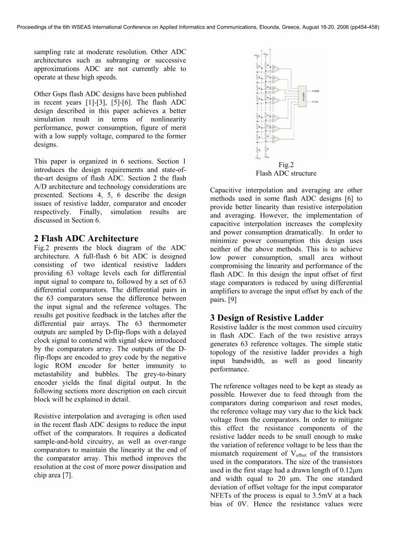
2 Flash ADC Architecture Fig.2 presents the block diagram of the ADC
architecture. A full-flash 6 bit ADC is designed
consisting of two identical resistive ladders
providing 63 voltage levels each for differential
input signal to compare to, followed by a set of 63
differential comparators. The differential pairs in
the 63 comparators sense the difference between
the input signal and the reference voltages. The
results get positive feedback in the latches after the
differential pair arrays. The 63 thermometer
outputs are sampled by D-flip-flops with a delayed
clock signal to contend with signal skew introduced
by the comparators array. The outputs of the D-
flip-flops are encoded to grey code by the negative
logic ROM encoder for better immunity to
metastability and bubbles. The grey-to-binary
encoder yields the final digital output. In the
following sections more description on each circuit
block will be explained in detail.
Resistive interpolation and averaging is often used
in the recent flash ADC designs to reduce the input
offset of the comparators. It requires a dedicated
sample-and-hold circuitry, as well as over-range
comparators to maintain the linearity at the end of
the comparator array. This method improves the
resolution at the cost of more power dissipation and
chip area [7].
Fig.2
Flash ADC structure
Capacitive interpolation and averaging are other
methods used in some flash ADC designs [6] to
provide better linearity than resistive interpolation
and averaging. However, the implementation of
capacitive interpolation increases the complexity
and power consumption dramatically. In order to
minimize power consumption this design uses
neither of the above methods. This is to achieve
low power consumption, small area without
compromising the linearity and performance of the
flash ADC. In this design the input offset of first
stage comparators is reduced by using differential
amplifiers to average the input offset by each of the
pairs. [9]
3 Design of Resistive Ladder Resistive ladder is the most common used circuitry
in flash ADC. Each of the two resistive arrays
generates 63 reference voltages. The simple static
topology of the resistive ladder provides a high
input bandwidth, as well as good linearity
performance.
The reference voltages need to be kept as steady as
possible. However due to feed through from the
comparators during comparison and reset modes,
the reference voltage may vary due to the kick back
voltage from the comparators. In order to mitigate
this effect the resistance components of the
resistive ladder needs to be small enough to make
the variation of reference voltage to be less than the
mismatch requirement of Voffset of the transistors
used in the comparators. The size of the transistors
used in the first stage had a drawn length of 0.12µm
and width equal to 20 µm. The one standard
deviation of offset voltage for the input comparator
NFETs of the process is equal to 3.5mV at a back
bias of 0V. Hence the resistance values were
Proceedings of the 6th WSEAS International Conference on Applied Informatics and Communications, Elounda, Greece, August 18-20, 2006 (pp454-458)

chosen to be equal to 970mΩ. The resistors where
implemented as L1 BEOL resistors because these
have the best absolute resistance tolerance and
mismatch. The small resistance meant that the
power consumption was a little higher but this was
required to achieve suitable reference voltage
variation trade-off.
4 Design of Comparator The critical consideration of comparator design is
the comparator mismatch. Given the non-ideal
fabrication technology, the comparator offset
voltage depends on variations in the width, length
and threshold voltage of the transistors. These three
factors tend to decrease if large transistors are used.
However increasing the size of transistors
introduces large input and parasitic capacitance. In
order to operate these devices at sufficient speed it
requires increased power consumption and
degradation in nonlinearity performance. Due to
the low supply voltage and voltage range limit
introduced from the former stages of the wireless
SoC, an input voltage range is only 300mV, which
requires the mismatch for Voffset to be less than 3.5
mV for the comparators in order to obtain a DNL
smaller than 0.75 LSB. This mismatch requirement
translates into large transistors in the comparators,
thus large capacitance, which slows down the
conversion speed and dissipates a large amount of
power. The input transistor sizes for the comparator
are equal to a drawn length of 0.12µm and width of
20µm.
The schematic of the differential comparator is
illustrated in Fig 3. The input stage comprises of
two differential pairs with diode connected loads
that measure and amplify the difference between
the positive/negative input signal and the reference
voltages.
Fig.3 Schematic of Differential Latched
Comparator
The regenerative latches provide positive feedback
to the output from the differential pairs to generate
comparison decision for the latter encoding stage.
During the period when the clock is low, the cross
connected nFETs amplify the voltage difference in
the differential pairs. Once the clock goes high, the
two nFETs are shorted and reset to the same
potential. To make the latches work fast, the size of
transistors in the latches are chosen to be as small
as possible to minimize the transistor capacitance
to increase the reset and transition speed between
reset mode and comparison mode.
Significant amounts of power are consumed in the
tail current sources biasing the transistors in the
comparator. The tail current sources need to be able
charge the differential pairs during the comparison
stage. Increasing the size of the tail current
transistors help with faster charging and
subsequently comparison speed but unfortunately
more power is consumed in each comparator.
In this design the tail current source transistor were
chosen to be equal to the smallest transistor size
that permitted the comparators to compare the
outputs at speed in the following three situation: (1)
Both input and reference voltage levels at the
maximum allowed input level, (2) Both input and
reference voltages at the minimum allowed input
level, and (3) one (input or reference) at the
maximum permitted input voltage whilst the other
at the lowest permissible voltage level.
5 Design of Encoder The encoding part of the ADC consists of four
stages: the thermometer code, 1-out-of-n code, grey
code and binary. First of all, the output of the
latched comparators is 63-bit thermometer code.
The thermometer code is converted into 1-out-of-
63 code by AND logic. In the 1-out-of-63 code,
only the transition from 1 to 0 is sensed and
translated to logic 1 by the AND gates, while others
are interpreted as logic 0. Then the negative logic
ROM encoder shown in Fig.4 converts the 1-out-
of-63 code into grey code. At the last encoding
stage, XOR gates are used to perform the
conversion from grey code to binary output.
Proceedings of the 6th WSEAS International Conference on Applied Informatics and Communications, Elounda, Greece, August 18-20, 2006 (pp454-458)

Fig. 4 Negative logic grey coded ROM
This four-stage encoding scheme described above
is deployed to overcome two main problems in the
encoder of a flash ADC, bubble errors and
metastability.
Bubble errors are mainly attributed to the
uncertainty of the sampling instant and comparator
offset voltage. When a bubble error occurs, an
erroneous zero is found between the series of ones
outputted from the thermometer code stage. In
order to avoid this situation the solution is to use
three-input AND gates instead of two-input ones
[3]. A decision basing on three thermometer inputs
effectively corrects the erroneous bubble. This
design does not contend with higher order bubbles
which are less likely to occur as large timing
mismatches between the different comparators is
relatively rare [1].
When the output of comparators is ambiguous,
neither logic 1 nor logic 0, downstream logic may
interpret these signal differently. This phenomenon
is so called metastability of comparator. In this
design, grey coded ROM is deployed instead of
binary coded ROM. Grey coded ROM handles
metastability errors better than binary coded ROM.
Three arrays of D-flip-flops are used in this design
at different stages of the ADC in order to force the
outputs to avoid the propagation of glitches. The
first array is placed after each latched comparator.
The second series of D-flip-flops follow the ROM
encoder. There are another six D-flip-flops at the
binary output stage to keep the outputs constant for
one clock cycle. Delay is introduced at each D-flip-
flop stage. As transition settling time varies
throughout the ADC, simulation has been done to
find out the minimum delay time in the D-flip-flops
without affecting latter stage process and the
overall system performance. For example, the
largest delay is set at the last D-flip-flop stage, due
to the large settling time in the grey-to-binary
encoder. The total delay brought in by D-flip-flops
is 1.15 ns operating at 1.2 GSPS.
In the used CMOS technology, the ratio between
the carrier mobility of the nFET and pFET
transistors is 3.7. The speed of the two types of
transistors needs to be adjusted to be the same to
make sure that the transition between logic 1 and
logic 0 passes the logic gates with the same settling
time. Therefore all digital logic gates are scaled at
the ratio between pFET and nFET as 4.
6 Simulation Result The simulations were run on the Cadence IC design
environment. The design was implemented in
130nm Bulk CMOS process (IBM CMRF8SF
utilizing 3 thin 2 thick front end of line copper
metal layers and 3 thick RF metal layers
comprising of 2 Aluminium and one copper layer).
The supply voltage was equal to 1.2V.
In the simulation, a ramp signal is applied to the
ADC. Fig.6 shows each transition step in the output
clearly. The DNL test shows an extremely good
linearity performance, illustrated in Fig.7. It has a
DNL less than 0.1 LSB and an INL less than 0.2
LSB. Dynamic simulation achieves an ENOB of
5.7 bits at 500MHz input signal at sampling
frequency to 1.2GSPS. The power dissipation of
the ADC is 65mW, where each comparator
consumes less than 1mW. The FoM of the ADC,
which is calculated by Power/(2ENOB
×2×ERBW), is
1.3pJ per conversion step. Table 1 shows a
summary of the ADC performance.
Fig.6 DC output response
Proceedings of the 6th WSEAS International Conference on Applied Informatics and Communications, Elounda, Greece, August 18-20, 2006 (pp454-458)

Fig.7 DNL simulation result
7 Conclusion In this paper a low-voltage high-speed low-power
ADC in 0.13µm is presented for multi Gigabit
wireless applications. The design operates at
1.2GSPS consuming 65mW of power delivering
5.7 ENOB. The figure of merit of the design is
1.3pJ per conversion.
References:
[1] K. Uyttenhove and M. S.J. Steyaert, A 1.8V 6-
Bit 1.3-GHz Flash ADC in 0.25µm CMOS, IEEE J.
Solid-State Circuits, vl 38, No.7, July 2003
[2] M. Choi and A. Abidi, A 6-bit 1.3-GSample/s
flash ADC in 0.35µm CMOS, IEEE J. Solid-State
Circuits, vol. 36, pp. 1847–1858, Dec.2001.
[3] P. Scholtens and M. Vertregt, A 6-b 1.6-GS/s
CMOS A/D converter, in IEEE Int. Solid-State
Circuits Conf. Dig. Tech. Papers, San Francisco,
CA, Feb. 2001, pp. 168–169.
[4] R. van de Plassche, CMOS Integrated Analog-
to-Digital and Digital-to-Analog Converters, 2nd
edition, Kluwer Academic Publishers, 2003
[5] G. Geelen, A 6b 1.1GSample/s CMOS A/D
Converter, ISSCC 2001, Session 8, Nyquist ADCs,
8.2
[6] C.Sandner, M. Clara, A. Santner, T. Hartig, F.
Kuttner, A 6-bit 1.2-GS/s Low-Power Flash-ADC
in 0.13-µm Digital CMOS, IEEE J. Solid State
Circuits, Vol. 40, No.7, July 2005
[7] A.Mahmoodi, High Speed Flash Analogue to
Digital Converters, Analog Integrated Circuit
Design, Dec 2005
[8] P.R. Kinget, Device Mismatch and Tradeoffs in
the Design of Analog Circuits, IEEE J. Solid State
Circuits, Vol.40, No.6, June 2005
[9] S.Sheikhaei, S.Mirabbasi, and A.Ivanov, A 4-bit
GS/s flash A/D Converter in CMOS, Proc. IEEE Int.
Symp. Circuits Syst. (ISCAS), May 2005, pp.6138-
6141.
Process IBM 0.13µm CMRF8SF
CMOS
VDD 1.2V
Sampling
rate
1.2 GSPS
Resolution 6 bit
DNL <0.1LSB (-0.0498/+0.085)
INL <0.5LSB
Input voltage
range
0.3V, differential
Power
Consumption
65mW
ENOB 5.7b @500MHz, 1.2GSPS
ERBW 500MHz @1.2GSPS
Table1. Performance summary of the flash ADC
Proceedings of the 6th WSEAS International Conference on Applied Informatics and Communications, Elounda, Greece, August 18-20, 2006 (pp454-458)