Embed Size (px)
Citation preview

A 107dB DR, 106dB SNDR Sigma-Delta ADC
Using a Charge-Pump Integrator for
Audio Application
By
Hubert, LIANG JUNHAO (DB029125)
Sam, JIANG DONGYANG(DB028791)
Final Year Project Report submitted in partial fulfillment
of the requirements for the Degree of
Bachelor of Science in Electrical and Electronics Engineering
2013/2014
Faculty of Science and Technology
University of Macau
ABSTRACT
Real world are full of analog signals, such as sound, light and color. After the electronic
revolution change came in, the magic brings novel device become a sort of clear
existence, like film, mobile, radio. Sure, we can imagine the first people hearing the
unclear voice from the telephone, the digital world is still a bounded existence with
noise and distortion. But as a development, people are expecting for clear information
and instructions, which means an extensive bridge between the analog and the digital
world.
To reach the goal, a high performance system which is called analog-to-digital converter
(ADC) is necessary. It is worked in electronic circuits at the interface between the
analog and the digital world. In this Final-Year-Project, we focus on the digital audio
conversion as we are probably pretty sure of being told that we're in the middle of a
digital audio revolution. In fact, for a hi-tech musician with an interest in computing
and digital audio hardware, chances are more aware of the possibilities than most people.
Comparing to other application like wireless communication, audio application covers
a relatively narrow bandwidth but needs high resolution, due to that, Sigma-Delta (Σ−Δ)
modulation based analog-to-digital (A/D) conversion technology is used in our system
design as a cost effective alternative for high resolution (greater than 12 bits) converters
which can be ultimately integrated on digital signal processor ICs. In this project, the
Cascaded Resonator with Distributed Feed Forward (CRFB) is selected because of its
high SNR and the narrow swing. Plus, a capacitive charge-pump is used to improve the
power efficiency of the first stage amplifier. By using 3rd order CRFB architecture with
charge-pump in the first stage, the simulated FOM is 204fJ/conversion-step from 1-V
supply. This CP based modulator gives 106dB peak-SNDR and 107dB dynamic range
over a 20 kHz bandwidth with 1.332mW power consumption, almost 32 % lower than
that of the convention one.
ACKNOWLEDGMENT
We cannot express enough thanks to our committee for their continued support and
encouragement: Supervisor Prof. Sin-Weng Sai, co-supervisor Prof. U Seng Pan,
Advisor U-Fat Chio, Advisor Arshad Hussain, and Advisor Fong Tek Kei. We offer our
sincere appreciation for the learning opportunities offered by my committee.
It is an honor for us that is given the opportunity to develop our own individuality and
self-sufficiency by being allowed to work with such independence. The experience
working in State-Key Laboratory of Analog and Mixed-Signal VLSI, University of
Macau will chase us for the future. If we have seen further it is by standing on the
shoulders of Giants.
We are grateful to many colleague for the completion of this project, all these people
read the evolving manuscript and circuits and offered advice. And because of their help,
we are content with the final result. Among them, we are particularly grateful to Qi
Liang, Wang Biao, for their reviewing the technical contexts and elaborative debugging.
Moreover, as a two people’s team, it was a great comfort and relief to know that we
were willing to share the working experience, we survived the experience of
undergraduate school and learned to work with encouragement and patience. We gained
so much a driving ability to tackle challenges. My heartfelt thanks.
Finally we would like to thank our families for their support and patience during the
past semesters which has taken me to graduate.

CONTENTS
I INTRODUCTION ................................................................................................. 1
1.1 Audio Application ....................................................................................... 1
1.2 Analog V.S. Digital ...................................................................................... 2
1.3 Background ................................................................................................. 3
1.4 Types of A/D Converter .............................................................................. 5
II BASIC THEORY OF SIGMA-DELTA ADC ...................................................... 8
2.1 Sampling ...................................................................................................... 8
2.2 Quantization ................................................................................................ 8
2.3 Oversampling ............................................................................................ 10
2.4 Noise Shaping ............................................................................................ 11
2.5 Digital Decimator...................................................................................... 13
III TARGET SPECIFICATION ....................................................................... 14
IV MODELING TECHNIQUE........................................................................ 16
4.1 Conventional Modulator Structure ........................................................ 16
A. The Boser-Wooley Modulator .............................................................. 16
B. The Silva-Steensgaard Structure ......................................................... 17
C. The Error-Feedback Structure ............................................................ 18
D. Summary ................................................................................................ 20
4.2 Advanced Modulator Structure .............................................................. 20
A. CIFB (Cascade Of Integrators With Distributed Feedback) ............ 20
B. CIFF (Chain of Integrators with Feed-Forward summation) .......... 22
C. CRFB (Cascade of Resonators with Distributed Feedback) ............. 24
D. CRFF ...................................................................................................... 28
E. Comparison ........................................................................................... 29
4.3 Multi-Stage Modulation ........................................................................... 30
A. The Leslie-Singh (L-0 Cascade) Structure .......................................... 30
B. MASH Modulator ................................................................................. 32
4.4 Analysis ...................................................................................................... 35
V NOISE ANALYSIS AND BEHAVIOR MODEL .............................................. 37
5.1 Noise analysis ............................................................................................ 37
A. Operational Amplifier Non-idealities .................................................. 39
B. Thermal and operation amplifier noise-Switches Thermal Noise

(kT/C) ............................................................................................................ 44
C. Operational Amplifier Noise ................................................................ 45
D. Clock Jitter ............................................................................................ 46
E. Overall noise .......................................................................................... 47
5.2 Behavioral model ...................................................................................... 49
VI CIRCUIT DESIGN ...................................................................................... 52
6.1 Charge Pump Integrator ......................................................................... 52
6.2 Op-Amp Design ........................................................................................ 56
6.3 Zero Optimization .................................................................................... 60
6.4 1.5 bit quantizer ........................................................................................ 61
6.5 Clock Generator ....................................................................................... 63
6.6 Feedback Logic ......................................................................................... 63
6.7 Switches Replacing ................................................................................... 64
VII PERFORMANCE ........................................................................................ 67
VIII CONCLUSION ............................................................................................ 72
IX REFERENCE ............................................................................................... 74
Statement Distribution
Hubert Sam
Common Part I,II,III,IV
6.1 Charge Pump Integrator
6.1 Charge Pump Integrator
Individual Part
V. noise analysis and behavior
model
6.2 Op-Amp Design
6.3 Zero Optimization
VII PERFORMANCE test
6.4 1.5 bit quantizer
6.5 Clock Generator
6.6 Feedback Logic
6.7 Switches Replacing

List of Tables
Table 1 Difference Between Analog And Digital Signal ........................................ 3
Table 2 Audio Sigma-Delta Adc From Ti [40] ...................................................... 14
Table 3 Automotive Audio ADC Product Of ADI And AKM [2] ......................... 15
Table 4 The SNR As The Coefficient Changes. .................................................... 20
Table 5 The SNR of different structure with single bit quantizer ......................... 27
Table 6 Comparison Between Feed Forward And Feedback Structure. ............... 29
Table 7 Comparison Between Single Loop And Multi-Loop Cascode ................. 36
Table 8 The Performance Of System As Gain Decrease ....................................... 41
Table 9 The Performance Of System As Sr And Gbw Change ............................. 42
Table 10 The Performance Of System As Saturation Voltage Change ................. 44
Table 11 The Performance Of System As Sampling Capacitance Change ........... 45
Table 12 Performance Of System As Input-Referred Operational Amplifier Noise
Change .......................................................................................................... 46
Table 13 The Performance Of System As Sampling Jitter Change ...................... 47
Table 14 System Performance With Different Noise ............................................ 47
Table 15 Behavior Model Of The Project ............................................................. 49
Table 16 New Gian Requirement Of First Op-Amp ............................................. 56
Table 17 1st op-amp performance ......................................................................... 58
Table 18 2nd Op-Amp Performance ..................................................................... 59
Table 19 3rd Op-Amp Performance ...................................................................... 60
Table 20 Comparison Of SR-Latch And Comparator ........................................... 62
Table 21 The Feedback Logic ............................................................................... 64
Table 22 Power Consumption For Each Part ........................................................ 69
Table 23 Comparison Of CP And Conventional ................................................... 70
Table 24 Performance Comparison With Other Switch Capacitor Sigma Delta
ADCs With Large OSR ................................................................................. 71
Table 25 The Performance Of System .................................................................. 72

List of Figures
Figure 1 The way people listen to music [41] ......................................................... 1
Figure 2 Professional Audio Applications [41] ....................................................... 2
Figure 3 The threshold of pain [16] ........................................................................ 4
Figure 4 Different types of ADCs ........................................................................... 5
Figure 5 The operating features of Different ADCs [4] .......................................... 6
Figure 6 Nyquist sampling theory ........................................................................... 8
Figure 7 2-bit resolution with four levels of quantization of a sine wave .............. 9
Figure 8 Sampling at twice the Nyquist rate ......................................................... 10
Figure 9 Block diagram of Sigma-Delta modulation [29] .................................... 11
Figure 10 Bode plot of noise transform function .................................................. 12
Figure 11 SNR vs OSR for sigma delta modulation ............................................. 13
Figure 12 Each operation of sigma delta ADC ..................................................... 13
Figure 13 The Boser-Wooley modulator ............................................................... 16
Figure 14 The simulation model of Boser-Wooley modulator with a1=0.5 a2=2 and
b=1 using single bit quantizer ....................................................................... 17
Figure 15 The Silva-Steensgaard Structure .......................................................... 17
Figure 16 The simulation circuit of Silva-Steensgaard Structure ......................... 18
Figure 17 Error-Feedback Structure ..................................................................... 18
Figure 18 The simulation circuit of Error-Feedback Structure ............................. 19
Figure 19 SNR performance of Error Feedback ................................................... 19
Figure 20 The CIFB Structure .............................................................................. 20
Figure 21 The simulation circuit of 2nd CIFB Structure (OSR=64) .................... 21
Figure 22 The CIFF structure ................................................................................ 22
Figure 23 The simulation circuit of 2nd order CIFF Structure with resonator ..... 24
Figure 24 The CRFB Structure ............................................................................. 24
Figure 25 The simulation circuit of 2nd order CRFB Structure ........................... 26
Figure 26 The CRFB Structure without delay ...................................................... 26
Figure 27 The resonator Structure without delay .................................................. 26
Figure 28 The simulation circuit of 2nd order CIFB Structure with resonator ..... 28
Figure 29 The CRFF structure .............................................................................. 28
Figure 30 The simulation result of 2nd order CRFF structure .............................. 29
Figure 31 The L-0 cascade (Leslie-Singh) structure ............................................. 30

Figure 32 Simulation result of the 2-0 cascade (Leslie-Singh) structure .............. 31
Figure 33 The L-0 cascade (Leslie-Singh) structure ............................................. 32
Figure 34 A MASH structure ................................................................................ 32
Figure 35 Simulation result of the 1-1 MASH structure ....................................... 33
Figure 36 Simulation result of the 2-1 MASH structure ....................................... 34
Figure 37 Simulation result of the 1-1-1 MASH structure ................................... 34
Figure 38 Simulation result of the 1-1-1-1 MASH structure ................................ 35
Figure 39 3rd order CRFB performance ............................................................... 37
Figure 40 The 3rd order CRFB with the noise block ............................................ 38
Figure 41 Switched capacitor integrator with finite gain op-amp ........................ 39
Figure 42 NTF of a second order modulator for three different dc gains of the op-
amps. ............................................................................................................. 40
Figure 43 The system performance With 54dB gain ............................................ 41
Figure 44 Response of a unity gain buffer with finite slew-rate and bandwidth .. 42
Figure 45 The system performance with GBW=50MHz and SR=30V/us ........... 43
Figure 46 The output of each integrator with Input amplitude is ±0.5 V ............. 43
Figure 47 The system performance 1V saturation voltage ................................... 44
Figure 48 The system performance with Cs=1pF ................................................. 45
Figure 49 The system performance with Vn=8.3uV ............................................. 46
Figure 50 The system performance ....................................................................... 48
Figure 51 Noise budget ......................................................................................... 48
Figure 52 3rd order CRFB architecture ................................................................ 49
Figure 53 The output swing of each integrator with Input amplitude is ±0.4 V ... 50
Figure 54 the system performance ........................................................................ 50
Figure 55 The 3rd order CRFB with noise block in matlab .................................. 50
Figure 56 The conventional CRFB circuit system ................................................ 51
Figure 57 (a) Conventional Switch capacitor integrator and (b) charge pump
integrator ....................................................................................................... 52
Figure 58 (c) Conventional Switch capacitor integrator and (d) charge pump
integrator during Φ2(integration phase) ........................................................ 53
Figure 59 The CRFB circuit system with CP integrator ....................................... 55
Figure 60 First op-amp structure ........................................................................... 56
Figure 61 The feedback test circuit ....................................................................... 57
Figure 62 The common mode feedback structure ................................................. 57

Figure 63 The baising circuit ................................................................................ 58
Figure 64 Second op-amp structure ...................................................................... 59
Figure 65 Second op-amp structure ...................................................................... 59
Figure 66 The SC local feedback .......................................................................... 60
Figure 67 Comparator schematic diagram ............................................................ 61
Figure 68 RS flip-flop ........................................................................................... 61
Figure 69 3-level-quantizer schematic .................................................................. 62
Figure 70 The clock generation logic ................................................................... 63
Figure 71 The feedback circuit ............................................................................. 64
Figure 72 MOSFET as a switch ............................................................................ 65
Figure 73 The transmission gate ........................................................................... 65
Figure 74 Fundamental principle of bootstrapped switch [37] ............................. 66
Figure 75 Bootstrapped Switch ............................................................................. 66
Figure 76 Bootstrapped switch with implementation ........................................... 67
Figure 77 Output PSD for the system ................................................................... 68
Figure 78 Output waveform .................................................................................. 68
Figure 79 Measured SNDR versus input amplitude ............................................. 69

List of Symbols
SYMBOL THE EXPLANATON
ADC Analog-to-Digital Convertor
A0 Open Loop Gain
CIFB Cascaded Integrators with Distributed Feedback
CIFF Cascaded Integrators with Distributed Feed Forward
CLK Clock Signal
CMFB Common-Mode Feedback
CP Charge-pump
CRFB Cascaded Resonator with Distributed Feed Forward
CRFF Cascaded Resonator with Distributed Feedback
DAC Digital-to-Analog Convertor
DR Dynamic Range
ENOB Effective-Number-of-Bit
fb Signal Bandwidth
fs Sampling Frequency
FoM Figure-of-merit
GBW Gain Bandwidth
GND Ground
NTF Noise Transfer Function
OSR Oversampling Ratio
PSD Power Spectrum Density
SNDR Signal-to-Noise and Distortion Ratio
SNR Signal-to-Noise Ratio
SQNR Signal-to-Quantization Noise Ratio
SR Slew-Rate
STF Signal Transfer Function
SW Switch
THD Total Harmonic Distortion
Vb Bias Voltage
Vcm-in Input Common-Mode Level
Vcm-out Output Common-Mode Level
VDD Supply Voltage
Vin Input Voltage
Vout Output Voltage
Vref Reference Voltage
V2n,Q Power of Quantization Noise
V2n,b Power of Quantization Noise within Signal Bandwidth
V2sin Power of Full-Scale Sine Wave
Φ Phase
Δ Quantization Step
ε Quantization Error

1
I INTRODUCTION
1.1 Audio Application
Real world are full of analog signals, such as sound, light and color. After the electronic
revolution change came in, the magic brings novel device become a sort of clear
existence. How many things could you shape out with digital clay? The answer seems
to be a very large number with scientists’ shading and decorating : telegram ,phone, fax,
e-mail, film, digital camera, CD player, smart cards, and so on and all so rapidly, so
continuously, that why it's always so exquisite and exciting to catch our breath.
During them I would like to examine audio in details. By age four, most humans have
developed an ability to communicate through oral language. These unique abilities of
communicating through a native language clearly separate humans from all animals.
That’s why voice, or audio, takes a special status in both analog and digital world.
Remember the first time you heard the music or your own voice from the speaker?
Melody and rhythm can trigger feelings from sadness to serenity to joy to awe; they can
bring memories from childhood vividly back to life. Maybe that’s why people are
favorite of music, and they are also persuading a better music device.
Figure 1 The way people listen to music [41]
So clearly one kind of important audio applications is coming from listeners, they are
looking forward to better music experience. Through Figure 1, from Gramophone to
CD player, new cellphone, listeners would no longer have to drive to store if they
wanted the latest album – it was available at the click of a mouse and was sometimes
2
cheaper than a physical CD. And from our experience people are now comfortable with
the idea of digital downloads and data syncing, and have grown used to surfing the
internet for music whenever they are in a Wi‑Fi hot spot. For them, the first need is
easier to carry as well as low power consumption.
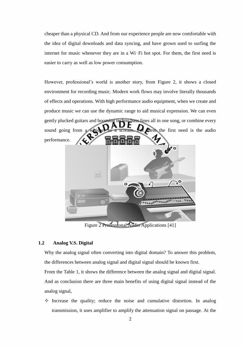
However, professional’s world is another story, from Figure 2, it shows a closed
environment for recording music. Modern work flows may involve literally thousands
of effects and operations. With high performance audio equipment, when we create and
produce music we can use the dynamic range to aid musical expression. We can even
gently plucked guitars and booming techno bass lines all in one song, or combine every
sound going from a whisper to a scream. For them the first need is the audio
performance.
Figure 2 Professional Audio Applications [41]
1.2 Analog V.S. Digital
Why the analog signal often converting into digital domain? To answer this problem,
the differences between analog signal and digital signal should be known first.
From the Table 1, it shows the difference between the analog signal and digital signal.
And as conclusion there are three main benefits of using digital signal instead of the
analog signal,
Increase the quality; reduce the noise and cumulative distortion. In analog
transmission, it uses amplifier to amplify the attenuation signal on passage. At the
3
same time, the cumulative distortion increase because the noise and error come from
surrounding environment also be amplified.
Save energy, use converter instead of the amplifier in transmission.
Information safety. We can use own method to encode and decode the signal. Given
the timing information, the transmitted waveform can be reconstructed.
Therefore, the analog signal are often converting into digital domain as the higher and
higher performance ADC are used in digital device nowadays.
Table 1 Difference Between Analog And Digital Signal
Analog Digital
Signal:
Continuous signal which
represents physical
measurements.
Discrete time signals generated
by digital modulation.
Waves: Denoted by sine waves Denoted by square waves
Representation: Uses continuous range of values Uses discrete or discontinuous
values
Example: Human voice in air, analog
electronic devices.
Computers, CDs, DVDs, and
other digital electronic devices.
1.3 Background
At the beginning, knowing the characteristic of the audio is important. Sound is a
mechanical wave that is an oscillation of pressure transmitted through some Medium.
The frequency range
For the body, ear is a magical part because it can help humans and animals to hear the
sound on around them. Sound cannot be seen, but it can be felt by vibrations. Hear sense
is one of the most important senses of the body. Sound actually consist of waves and
vibrations. Sound travels through the media such as air, the ground, the water, and some
solid.
Frequency is the number of vibrations that are produced per second. The unit of the
frequency is hertz which is described vibration per second. A low frequency sound will

4
have a low pitch, such as the sound when knock the door. While a high frequency sound
will have a high pitch, a dolphin bark is a good example. However, humans cannot hear
sounds in very high as well as very low frequency. 20 to 20,000 hertz for a healthy
young person is the hearing range. [33]
Hearing range of humanity
Sound pressure level (SPL) or sound level is a logarithmic measure of the effective
sound pressure of a sound relative to a reference value. It is measured in decibels (dB)
above a standard reference level. The standard reference sound pressure in air or other
gases is 20 µPa, which is usually considered the threshold of human hearing (at 1 kHz).
[16]
Then we collect data for the opposite extreme, the 'threshold of pain. This is the point
where the audio amplitude is so high that the ear's physical and neural hardware is not
only completely overwhelmed by the input, but experiences physical pain. Collecting
this data is trickier. You don't want to permanently damage anyone's hearing in the
process.
Figure 3 The threshold of pain [16]
CD standard
CD is a common application of the audio. And it develops many years so there is a quite
formal standard of the audio. From the CD standard, we can know about the audio
standard which is used in music industry. So that it is helpful to know more about the
audio. Compact Disc Digital Audio (CDDA or CD-DA) is the standard format for audio
Compact Discs. The standard is defined in the Red Book. [43]
16 bit (CD standard)

5
Form the previous part, the sound amplitude that can be perceived by human ear is
between 0 dB SPL and 130 dB SPL. Supposing the normal condition, the music that we
daily heard is between 10 and 100db SPL (which is actually very high, possible screw
people’s ears), yields a dynamic range of 90 dB. That’s why CD standard is enough for
being distributed to consumers, and keeps itself for a very long time
24 bit (SACD or DSD)
But for professional, actually it's another story, Professionals use 24 bit samples in
recording for headroom, noise floor, and convenience reasons like equipment matching.
Also, re-production, which means mixing or mastering, needs high resolution than
people’s normal thinking.
DSD or SACD cancels the PCM part, it records the data at a very high rate with one-bit
style. This Specifications’ benefit can be well showed in the process of trying to
maintain data integrity. And this is just how the high speed ADC works. This standard
is advanced and well adopted by markets.
1.4 Types of A/D Converter
Figure 4 Different types of ADCs
It seems to be a formidable task to select the proper ADC for a particular application,
considering the thousands of converters currently on the market. Going right to the
selection guides and parametric search engines is a direct approach, such as those
available on the Analog Devices website. Type some key words such as ‘sampling rate’,
‘resolution’, ‘power supply voltage’ as well as other important properties, and click the
6
‘find’ button to hope for the best. It’s not enough obviously. How to find a ‘best choice’
for the project as well as the application? The important approach is to get greater
understanding for the task as well as the ADC.
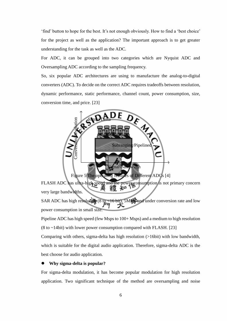
For ADC, it can be grouped into two categories which are Nyquist ADC and
Oversampling ADC according to the sampling frequency.
So, six popular ADC architectures are using to manufacture the analog-to-digital
converters (ADC). To decide on the correct ADC requires tradeoffs between resolution,
dynamic performance, static performance, channel count, power consumption, size,
conversion time, and price. [23]
Sigma Delta
SAR
Subranging/Pipelined
Signal Bandwidth
Co
nv
ersi
on
Res
olu
tio
n
Figure 5 The operating features of Different ADCs [4]
FLASH ADC has ultra-high speed and the power consumption is not primary concern
very large bandwidths.
SAR ADC has high resolution (8 to <16 bit), 5Msps and under conversion rate and low
power consumption in small size.
Pipeline ADC has high speed (few Msps to 100+ Msps) and a medium to high resolution
(8 to ~14bit) with lower power consumption compared with FLASH. [23]
Comparing with others, sigma-delta has high resolution (>16bit) with low bandwidth,
which is suitable for the digital audio application. Therefore, sigma-delta ADC is the
best choose for audio application.
Why sigma-delta is popular?
For sigma-delta modulation, it has become popular modulation for high resolution
application. Two significant technique of the method are oversampling and noise

7
shaping. Therefore the analog signals can be converted by using a 1-bit ADC only.
Though concepts of sigma-delta modulation have proposed from the Middle of the
century, but this method has become more attractive only in the last two decades. The
important reason is that development in VLSI technology nowadays focuses on building
high speed, high intensive packed digital circuits, and it made possible the suitable
digital processing into the bit stream. At low to medium signal bandwidths, it can obtain
high resolution by using sigma delta modulation. [21]
All in all, sigma delta ADC is a perfect choice to the audio application.

8
II BASIC THEORY OF SIGMA-DELTA ADC
2.1 Sampling
The digital side of a sigma-delta converter, which is what makes the sigma-delta ADC
inexpensive to produce, is more complex. It performs filtering and decimation. To
understand how it works, we must become familiar with the concepts of oversampling,
noise shaping, digital filtering, and decimation. Especially, the oversampling and noise
shaping is technique of sigma-delta ADC.
In order to learn about oversampling, it should be first know that Nyquist rate
conversion, in signal processing, sampling is the reduction of a continuous signal to
discrete signal.
𝑋𝑠(𝑓) =1
𝑇𝑠∑ 𝑋(𝑓 − 𝑘𝑓𝑠)∞
𝑘=−∞ (1)
(𝑓s) represents the spectrum of the sampled signal.
(𝑓) represents the spectrum of the original continuous time signal.
For Nyquist ADC, sampling frequency fs should be double of the bandwidth fB
according to the Nyquist theory. [29]
Nyquist rate fs=2fB
fB fs 2fs
Signal spectrum
Repeated versions of the signal spectrum
Required anti-aliasing filter response
Figure 6 Nyquist sampling theory
In the sampling process, it is sampled at uniformly spaced time intervals T for a
continuous time signal, The samples of the continuous time signal can be represented
as x[n] = x(nT), where x[n] is the samples and x(t)is the continuous time signal. In the
frequency domain, the effect of the sampling process is to create versions of the signal
spectrum repeated at multiples of the sampling frequency = l/T periodically. [31]
2.2 Quantization

9
Amplitude quantization changes a sampled-data signal from continuous-level to
discrete-level. The quantized output amplitudes are usually represented by a digital code
word composed of a finite number of bits. The digital code words are often said to be
in pulse code modulation (PCM) format. [3]
Figure 7 2-bit resolution with four levels of quantization of a sine wave
In analog-to-digital conversion, the difference between the actual analog value and
quantized digital value is called quantization error or quantization distortion. This error
is either due to rounding or truncation. The error signal is sometimes considered as an
additional random signal called quantization noise. The power density spectrum is
𝑝(𝜀𝑄) = {
1
∆, 𝑓𝑜𝑟 𝜀𝑄 ∈ −
∆
2… . .
∆
2
0, 𝑜𝑡ℎ𝑒𝑟𝑤𝑖𝑠𝑒 (2)
And the error here is a white noise, the error sequence, e[n], is a sample sequence of a
stationary random process. The quantization noise power is
𝑃𝑄 = ∫ 𝜀𝑄2. 𝑝
∞
−∞(𝜀𝑄) d𝜀𝑄 = ∫
𝜀𝑄2
∆𝑑𝜀𝑄 =
∆2
12
∆
2−∆
2
(3)
Signal to noise ratio
The effect of noise is quantified by the signal-to-noise ratio (SNR) defined by
𝑆𝑁𝑅| 𝑑𝐵
= 10𝑙𝑜𝑔𝑃𝑠𝑖𝑔𝑛
𝑃𝑛𝑜𝑖𝑠𝑒 (4)
Where 𝑃𝑠𝑖𝑔𝑛 and 𝑃𝑛𝑜𝑖𝑠𝑒 are the power of the signal and the power of the noise in the
band of interest.
Sine wave as example,

10
𝑃𝑠𝑖𝑛𝑒 =1
𝑇∫
𝑋𝐹𝑆2
4𝑠𝑖𝑛2(2𝜋𝑓𝑡)𝑑𝑡
𝑇
0≈
1
𝑇∫
𝑋𝐹𝑆2
4(2𝜋𝑓𝑡)2𝑑𝑡
𝑇
0=
(∆∙2𝑛)2
8 (5)
And 𝑃𝑄 =∆2
12
𝑆𝑁𝑅𝑠𝑖𝑛𝑒| 𝑑𝐵
= (6.02 ∙ 𝑛 + 1.78)𝑑𝐵 (6)
From the SNR equation, it can be concluded that every bit of the resolution improves
the signal to noise ratio by 6.02 dB which is about 4 times improve.
2.3 Oversampling
Oversampling is the process of sampling a signal with a sampling frequency
significantly higher than twice the bandwidth or highest frequency of the signal being
sampled.
Sampling at twice Nyquist
rate fs=4fB
fB
Signal spectrum
Repeated versions of the signal spectrum
Required anti-aliasing filter response
fs
Figure 8 Sampling at twice the Nyquist rate
Another benefit directly caused by oversampling is that the requirement of the shape of
the analog anti-aliasing filter can be decrease. It can be seen that a signal is sampled at
twice the Nyquist rate in Figure 8. On this occasion, the anti-aliasing filter can have a
transition band which is between fs/2 and fB if it can provides very good attenuation
beyond fs/2
The SNR calculation on oversampling A/D converter: [4]
𝑂𝑆𝑅 =𝑓𝑠
2𝑓𝐵 (7)
In band noise power
𝜎𝑒𝑦2 = ∫ 𝑃𝑒𝑦(𝑓)𝑑𝑓
𝑓𝐵
−𝑓𝐵= 2 ∫ 𝑃𝑒𝑦(𝑓)𝑑𝑓
𝑓𝐵
0= ∫
2𝜎𝑒2
𝑓𝑠𝑑𝑓 = 𝜎𝑒
2(2𝑓𝐵
𝑓𝑠)
𝑓𝐵
0 (8)
Where 𝜎𝑥 2 the input is signal power and define 𝑂𝑆𝑅 = 2𝑟.

11
𝑆𝑁𝑅 = 10 𝑙𝑜𝑔 (𝜎𝑥
2
𝜎𝑒𝑦2 )
= 10 𝑙𝑜𝑔(𝜎𝑥2) − 10 𝑙𝑜𝑔(𝜎𝑒𝑦
2 ) + 3.01𝑟 (9)
Every doubling of the OSR, the SNR improves by about 3dB which is one-half bit
resolution improve.
All in all, Oversampling helps avoid aliasing, improves resolution, and reduces noise
and the anti-aliasing filter dose net need as sharp a cutoff.
2.4 Noise Shaping
Noise shaping is a technique which reduces the in-band noise by incorporating in a
feedback loop, which is the one of the key technique on the sigma delta ADC.
Z-1
DAC
x[n] u[n] v[n]
e[n]
y[n]
ya[n]B
A
B
Figure 9 Block diagram of Sigma-Delta modulation [29]
From the block diagram, the noise transform function can be found
[𝑋 − 𝑌 ∙ 𝐵(𝑧)]𝐴(𝑧) + 𝜀𝑄 = 𝑌
𝑌 =𝑋 ∙ 𝐴(𝑧)
1 + 𝐴(𝑧)𝐵(𝑧)+
𝜀𝑄
1 + 𝐴(𝑧)𝐵(𝑧)
𝑁𝑇𝐹(𝑧) =𝑌
𝜀𝑄=
1
1+𝐴(𝑧)𝐵(𝑧) (10)
Where 𝐴(𝑧) =𝑧−1
1−𝑧−1and 𝐵(𝑧) = 1
Therefore the noise transform function is
𝑁𝑇𝐹(𝑧) = 1 − 𝑧−1
12
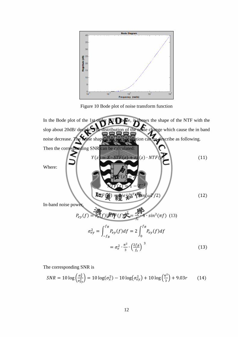
Figure 10 Bode plot of noise transform function
In the Bode plot of the 1st order NTF above, it shows the shape of the NTF with the
slop about 20dB/ decade. The distribution of the noise change which cause the in band
noise decrease. The noise shape after each operation can be describe as following.
Then the corresponding SNR can be calculated:
𝑌(𝑧) = 𝑋 ∙ 𝑆𝑇𝐹(𝑧) + 𝜀𝑄(𝑧) ∙ 𝑁𝑇𝐹(𝑧) (11)
Where:
𝑆𝑇𝐹(𝑧) = 𝑍−1
𝑁𝑇𝐹(𝑧) = 1 − 𝑍−1
𝑁𝑇𝐹(𝜔) = 2𝑗𝑒−𝑗𝜔𝑇/2𝑠𝑖𝑛 (𝜔𝑇/2) (12)
In-band noise power,
𝑃𝑒𝑦(𝑓) = 𝑃𝑒(𝑓)|𝑁𝑇𝐹(𝑓)| 2
=𝜎𝑒
2
𝑓𝑠∙ 4 ∙ 𝑠𝑖𝑛2(𝜋𝑓) (13)
𝜎𝑒𝑦2 = ∫ 𝑃𝑒𝑦(𝑓)𝑑𝑓
𝑓𝐵
−𝑓𝐵
= 2 ∫ 𝑃𝑒𝑦(𝑓)𝑑𝑓𝑓𝐵
0
= 𝜎𝑒2 ∙
𝜋2
3∙ (
2𝑓𝐵
𝑓𝑠)
3
(13)
The corresponding SNR is
𝑆𝑁𝑅 = 10 log (𝜎𝑥
2
𝜎𝑒𝑦2 ) = 10 log(𝜎𝑥
2) − 10 log(𝜎𝑒𝑦2 ) + 10 log (
𝜋2
3) + 9.03𝑟 (14)

13
0
20
40
60
80
100
120
4 8 16 32 64 128 256
Oversampling Ratio, OSR
512
1st order
2nd
order
3rd
order
140
SN
R(d
B)
Figure 11 SNR vs OSR for sigma delta modulation
From equation of SNR above, if oversampling ratio is double which means increase the
r the SNR improves about 9 dB, and the resolution increase about 1.5 bits equivalently.
That is better than the Nyquist ADC.
For the second order, if the oversampling ratio is double the SNR will increase about
15dB. Moreover the SNR performance of sigma delta modulation can increase about
21dB if the oversampling ratio is double for the third order modulation.
ADC
fs
A
fs/2 fs
Nyquist Operation
ADC
kfs
B
fs/2 kfs/2
Oversampling
+ Digital filter
Digital
filter
ƩΔMOD
kfs
fs/2 kfs/2
Oversampling
+ Digital filter
+ Noise shaping
Digital
filter
C
kfs
kfs
Figure 12 Each operation of sigma delta ADC
2.5 Digital Decimator
The digital decimator consists of low pass filter and down sampler, the usages of the
decimator:
• Filter the noise after noise shaping
• Anti-aliasing, cancel the out-band noise
• Reduce the ADC data rate of output
This one is not needed for our design, which will be talked later.

14
III TARGET SPECIFICATION
In order to design the system as well as the further circuit of this project, setting the
target specification is necessary after known the sigma-delta technique (oversampling
and noise shaping) and its characteristic.
In this project, the target is to design a high performance ƩΔ ADC in audio application.
The specification should be basic on the audio application. For different application, the
ADCs have different requirement.
In general, it separate the products as the ‘home audio’, ‘portable audio’ and
‘professional audio’. [40] The products that mostly draw people attention must be
portable product such as mobile phone, mp3. And the high quality audio portable
product is required in car audio system because of the closed environment of the car. So
we want to design a sigma-delta ADC for the car audio system which is similar to the
home hi-fi system. The following part is the specification of some actual products from
different company, which is a good reference to make further decision about the
specification.
Table 2 Audio Sigma-Delta Adc From Ti [40]
SNR sampling rate(max) power (chip)
pcm1802 105dB 96kHz 147mW
pcm1803a 103dB 96kHz 60mW
pcm1804 111dB 96kHz 225mW
pcm1804-q1 112dB 192kHz 225mW
pcm1807 99dB 96kHz 62mW
pcm1808 99dB 96kHz 62mW
pcm1808-q1 99dB 96kHz 62mW
pcm1851a 101dB 96kHz 160mW
professional
PCM4202 118dB 216KHz 308mW
PCM4204 118dB 216KHz 600mW
PCM4220 123dB 216KHz 305mW
portable
PCM4201 112dB 108KHz 49mW
PCM1870A* 90dB 50KHz 40mW
tlv320adc3001 96dB 96KHz 17mW

15
From the table, the pcm1808 are the audio ADCs use in car audio system. The SNR
performance is 99dB.
Table 3 Automotive Audio ADC Product Of ADI And AKM [2]
Bits Max fs(kHz) S/N(dB)
AK5355VN 16 50 91
AK5355VT 16 50 91
AK5357KT 24 96 102
AK5357VT 24 96 102
AK5359VT 24 216 102
AK5381VT 24 96 106
AK5384VF 24 96 107
AK5385BVF 24 216 114
AK5386VT 24 216 110
AK5701KN 16 48 89
AK5730VQ 24 48 100
ADI
AD1871 24 96 105
AD1877 16 48 94
ADAU1977 24 192 106
AD1974 24 192 105
From the two table above, the SNR performance of the ADCs are usually greater than
100dB. Moreover, the target of this project is to design a higher performance one.
Therefore, we set our target of the SNR performance to 105dB. After setting the target,
the structure of the ƩΔ ADC will be chosen to build the system so that we can achieve
our target. The difference between each structure will discusses in following part.

16
IV MODELING TECHNIQUE
4.1 Conventional Modulator Structure
To choose the structure, the basic of different structure modulators should be learnt.
Here start from the conventional second order modulator which are basic and easier to
understand and simulate. [38]
A. The Boser-Wooley Modulator
A second-order modulator with two delaying integrators is called the Boser-Wooley
modulator. [36]
Z-1
DAC
u[n]a1 Z
-1
b
Q
Y V
Figure 13 The Boser-Wooley modulator
STF(z) =𝑎1𝑎2𝑧−2
𝐷(𝑧) and NTF(z) =
(1−𝑧−1)2
𝐷(𝑧)
D(z) = (1 − 𝑍−1)2 + 𝑎2b𝑍−1(1 − 𝑍^(−1)) + 𝑎1𝑎2𝑍−2 (15)
The parameter a1a2=1 and a2b=2, then use the example in the book to build the Matlab
model. In the actual design process, dynamic range scaling removes any ambiguity in
finding the parameters needed to implement a given NTF and STF.
-2 -1 0 1 2
0
50
100
150
200
250First Integrator Output
Voltage [V]
Occurr
ences
-5 0 50
20
40
60
80
100
120
140
160
180
200Second Integrator Output
Voltage [V]
Occurr
ences

17
Figure 14 The simulation model of Boser-Wooley modulator with a1=0.5 a2=2 and
b=1 using single bit quantizer
It allows the op amps in each integrator to settle independently of each other, thereby
relaxing their speed requirements. It has two feedback paths, two signal feedback into
the each input of the integrator. Therefore, the swing of output of integrator is high.
B. The Silva-Steensgaard Structure
The Silva-Steensgaard Structure actually is a second order modulator with feed-forward
paths. The distinguishing features of this circuit are the direct feed-forward path from
the input to the quantizer and the single feedback path from the digital output linear
analysis confirms that the output is given in the z-domain by as before.
Z-1
DAC
u[n]
Z-1
Q
Y V
1
1
2
Figure 15 The Silva-Steensgaard Structure
V(z) = U(z) + (1 − 𝑧−1)2𝐸(𝑧) (16)
The input signal to the loop filter is, however, different: it contains only the shaped
quantization noise:
U(z) − V(z) = −(1 − 𝑧−1)2𝐸(𝑧) (17)
0 1 2 3 4 5 6 7 8
x 104
-200
-180
-160
-140
-120
-100
-80
-60
-40
-20
0PSD of a 2nd-Order Sigma-Delta Modulator (detail)
Frequency [Hz]
PS
D [
dB
]
SNR = 69.6dB @ OSR=64
ENOB = 11.27 bits @ OSR=64
18
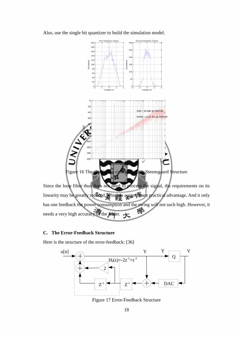
Also, use the single bit quantizer to build the simulation model.
Figure 16 The simulation circuit of Silva-Steensgaard Structure
Since the loop filter thus does not need to process the signal, the requirements on its
linearity may be greatly reduced, which is a significant practical advantage. And it only
has one feedback the power consumption and the swing will not such high. However, it
needs a very high accuracy of the adder.
C. The Error-Feedback Structure
Here is the structure of the error-feedback: [36]
DAC
u[n]Q
Y V
Z-1
Z-1
2
Hf(z)=-2z-1
+z-2
Y
Figure 17 Error-Feedback Structure
-2 -1 0 1 20
20
40
60
80
100
120
140
160
180
200First Integrator Output
Voltage [V]O
ccur
renc
es-4 -2 0 2 4
0
50
100
150
200
250
300Second Integrator Output
Voltage [V]
Occ
urre
nces
103
104
105
106
-200
-180
-160
-140
-120
-100
-80
-60
-40
-20
0PSD of a 2nd-Order Sigma-Delta Modulator
Frequency [Hz]
PS
D [
dB
]
SNR = 69.8dB @ OSR=64
ENOB = 11.31 bits @ OSR=64

19
𝑁𝑇𝐹 = 1 + 𝐻𝑓(𝑧)
To obtain
𝑁𝑇𝐹 = (1 − 𝑧−1)2
The H (f) should be
𝐻𝑓(𝑧) = (1 − 𝑧−1)2 − 1 = −2𝑧−1 + 𝑧−2 (18)
Use the single bit quantizer to build the simulation model. And this example looks
simple and hence attractive, but it is impractical for the analog sigma delta loops. We
can see the reason in the simulation performance.
Figure 18 The simulation circuit of Error-Feedback Structure
In practice, even with careful analog design, the achievable ENOB will typically be less
than 10 bits for ADCs with a single-bit quantizer, even for high OSR.
Figure 19 SNR performance of Error Feedback
For this structure, it is not practical for analog implementation, since it is very sensitive
to variations of its parameters.
-4 -2 0 2 40
50
100
150
200
250
300First Integrator Output
Voltage [V]
Occ
urre
nces
-5 0 50
50
100
150
200
250Second Integrator Output
Voltage [V]
Occ
urre
nces
0 1 2 3 4 5 6 7 8
x 104
-200
-180
-160
-140
-120
-100
-80
-60
-40
-20
0PSD of a 2nd-Order Sigma-Delta Modulator (detail)
Frequency [Hz]
PS
D [
dB
]
SNR = 70.7dB @ OSR=64
ENOB = 11.45 bits @ OSR=64
20
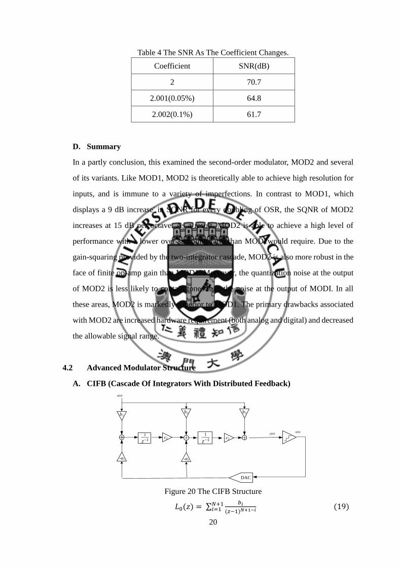
Table 4 The SNR As The Coefficient Changes.
Coefficient SNR(dB)
2 70.7
2.001(0.05%) 64.8
2.002(0.1%) 61.7
D. Summary
In a partly conclusion, this examined the second-order modulator, MOD2 and several
of its variants. Like MOD1, MOD2 is theoretically able to achieve high resolution for
inputs, and is immune to a variety of imperfections. In contrast to MOD1, which
displays a 9 dB increase' in SQNR for every doubling of OSR, the SQNR of MOD2
increases at 15 dB per octave. As a result, MOD2 is able to achieve a high level of
performance with a lower over sampling ratio than MOD1would require. Due to the
gain-squaring provided by the two-integrator cascade, MOD2 is also more robust in the
face of finite op-amp gain than MOD1. Moreover, the quantization noise at the output
of MOD2 is less likely to contain tones than the noise at the output of MODI. In all
these areas, MOD2 is markedly superior to MOD1. The primary drawbacks associated
with MOD2 are increased hardware requirement (both analog and digital) and decreased
the allowable signal range.
4.2 Advanced Modulator Structure
A. CIFB (Cascade Of Integrators With Distributed Feedback)
b2b1
c1 c2
DAC
b3
-a1 -a2
v(n)y(n)
u(n)
1
1Z
1
1Z
Figure 20 The CIFB Structure
𝐿0(𝑧) = ∑𝑏𝑖
(𝑧−1)𝑁+1−𝑖𝑁+1𝑖=1 (19)

21
And the L1 is
𝐿1(𝑧) = ∑−𝑎𝑖
(𝑧−1)𝑁+1−𝑖 𝑁𝑖=1 (20)
According to the general structure
NTF(z) =1
1−𝐿1(𝑧)=
(𝑧−1)𝑁
𝐷(𝑧) (21)
STF(z) =𝐿0(𝑧)
1−𝐿1(𝑧)=
𝑏1+𝑏2(𝑧−1)+⋯+𝑏𝑁+1(𝑧−1)𝑁
𝐷(𝑧) (22)
Feedback coefficients a’s realize the zeroes of L1 and thus the NTF and STF poles.
Feed-in coefficients b’s determine zeroes of L0 and thus the STF zeroes.
State scaling coefficients c’s are used for dynamic range scaling.
Implements Butterworth NTF.
Build the 2nd order model as example with single bit quantizer:
Figure 21 The simulation circuit of 2nd CIFB Structure (OSR=64)
103
104
105
106
-200
-180
-160
-140
-120
-100
-80
-60
-40
-20
0PSD of a 2nd-Order Sigma-Delta Modulator
Frequency [Hz]
PS
D [
dB
]
SNR = 70.7dB @ OSR=64
ENOB = 11.45 bits @ OSR=64
22
B. CIFF (Chain of Integrators with Feed-Forward summation)
b2b1
DAC
b3
y(n)
u(n)
1
1Z
1
1Z
-c1
c2 a2
a1
Figure 22 The CIFF structure
Instead of using a feedback structure to realize the loop-filters L0 and L1 given by
Equations mentioned last, a feed-forward structure can also be employed. Figure 1
shows a third-order modulator with delaying integrators and feed-forward branches.
This topology is called Chain of Integrators with Feed-Forward summation (CIFF).
We can observe that the feedback filter transfer function is given
𝐿1(𝑧) = ∑−𝑎𝑖
(𝑧−1)𝑁+1−𝑖𝑁𝑖=1 (23)
Similarly, the input transfer function is given
𝐿0(𝑧) =𝑟1+𝑟2(𝑧−1)+⋯+𝑟𝑁(𝑧−1)𝑁−1+𝑟𝑁+1(𝑧−1)𝑁
(𝑧−1)𝑁 (24)
Where
𝑟1 = 𝑏1𝑎𝑁 𝑟𝑁 = 𝑏1𝑎1 + 𝑏2𝑎2 … … 𝑟𝑁+1 = 𝑏𝑁+1 (25)
There are some typical cases
𝑏2 = 𝑏3 = ⋯ = 𝑏𝑁 = 0 𝑎𝑛𝑑 𝑏1 = 𝑏𝑁+1 = 1
𝐿0(𝑧) = 1 − 𝐿1(𝑧)
Further, when 𝑏𝑁+1 = 1
𝐿0(𝑧) = 1 − 𝐿1(𝑧)
𝑆𝑇𝐹(𝑧) =𝐿0(𝑧)
1−𝐿1(𝑧)= 1 (26)
𝑁𝑇𝐹(𝑧) =1
1−𝐿1(𝑧) (27)

23
And when 𝑏𝑁+1 = 0
𝐿0(𝑧) = −𝐿1(𝑧)
𝑆𝑇𝐹(𝑧) = 1 − 𝑁𝑇𝐹(𝑧) =−𝐿1(𝑧)
1−𝐿1(𝑧) (28)
𝑁𝑇𝐹(𝑧) =1
1−𝐿1(𝑧) (29)
Cascade of delaying integrators:
Feedforward coefficients a’s realize the zeroes of L1 and thus the NTF and STF
poles.
Feed-in coefficients b’s determine zeroes of L0 and thus the STF zeroes.
State scaling coefficients c’s are used for dynamic range scaling.
The 2nd order model as example, the simulation of CIFF is done with resonator. Uses
resonators formed with two delaying integrators. Resonator poles outside the unit circle
𝑧𝑖 = 𝑒1±𝑗√𝑔1

24
Figure 23 The simulation circuit of 2nd order CIFF Structure with resonator
C. CRFB (Cascade of Resonators with Distributed Feedback)
1
Z
Z
b2b1
c1 c2
DAC
b3
-a1 -a2
v(n)y(n)
u(n)
1
1Z
-g1
Figure 24 The CRFB Structure
Characteristic of this structure:
Combine a non-delaying and a delaying integrator with local feedback around
them, to form a stable resonator.
Local feedback coefficients g’s realize the complex zeroes in the NTF.
Implements NTF with complex zeroes.
For odd-order, use an integrator in the front to avoid noise coupling due to g.
To know how the g realize the complex zeroes in the NTF, I analyze the resonator.
c1
1
1Z
-g1
u(n)y(n)
1
Z
Z
Figure The resonator Structure
103
104
105
106
-200
-180
-160
-140
-120
-100
-80
-60
-40
-20
0PSD of a 2nd-Order Sigma-Delta Modulator
Frequency [Hz]
PS
D [
dB
]
SNR = 74.5dB @ OSR=64
ENOB = 12.09 bits @ OSR=64

25
Original:
𝑌(𝑧) =𝑧
(𝑧−1)2 𝑈(𝑧) (30)
𝐻(𝑧) =𝑌(𝑧)
𝑈(𝑧)=
𝑧
(𝑧−1)2 (31)
Poles: z=1; Resonator:
𝑌(𝑧) =𝑧
(𝑧−1)2 𝑈(𝑧) −𝑔𝑧
(𝑧−1)2 𝑌(𝑧) (32)
𝑅(𝑧) =𝑌(𝑧)
𝑈(𝑧)=
𝑧
𝑧2 − (2 − 𝑔)𝑧 + 1
=𝑧
(𝑧−𝑒𝑗𝛼)(𝑧−𝑒−𝑗𝛼) (33)
Where 𝛼 = 𝑐𝑜𝑠−1(1 −𝑔
2) and sin (
𝛼
2) = ± √𝑔
2
𝛼 ≈ ±√𝑔 (34)
The poles become 𝑧 = 𝑒±𝑗√𝑔 actually is the zeros of NTF. Build the 2nd order model
as example,

26
Figure 25 The simulation circuit of 2nd order CRFB Structure
CRFB Without Delay
b2b1
c1 c2
DAC
b3
-a1 -a2
v(n)y(n)
u(n)
1
1Z
1
1Z
-g1
Figure 26 The CRFB Structure without delay
Characteristic of this structure:
A resonator can also be formed with two delaying integrators
Resonator poles outside the unit circle.
Locally unstable but works fine in a stable loop-filter.
Relaxes settling requirements on the op-amps and implements complex NTF zeroes.
Also, analyze the resonators
c11
1Z
1
1Z
-g1
u(n)y(n)
Figure 27 The resonator Structure without delay
Original:
103
104
105
106
-200
-180
-160
-140
-120
-100
-80
-60
-40
-20
0PSD of a 2nd-Order Sigma-Delta Modulator
Frequency [Hz]
PS
D [
dB
]
SNR = 72.5dB @ OSR=64
ENOB = 11.75 bits @ OSR=64
27
Y(z) =1
(z−1)2 U(z) (35)
H(z) =Y(z)
U(z)=
1
(z−1)2 (36)
Poles: z = 1
Resonator:
Y(z) =1
(z−1)2 U(z) −g
(z−1)2 Y(z) (37)
R(z) =Y(z)
U(z)=
1
z2−2z+g+1 (38)
Where tan(𝛼) = ±√𝑔 and 𝛼 ≈ ±√𝑔
Poles:
𝑧 = 1 ± 𝑗√𝑔 (39)
Which are out of the unit circle.
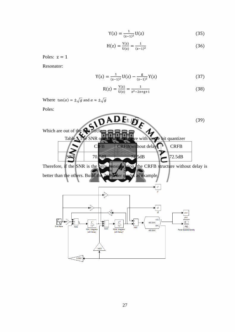
Table 5 The SNR of different structure with single bit quantizer
CIFB CRFB(without delay) CRFB
SNR 70.7dB 74.5dB 72.5dB
Therefore, if the SNR is the only consideration, the CRFB structure without delay is
better than the others. Build the 2nd order model as example,

28
Figure 28 The simulation circuit of 2nd order CIFB Structure with resonator
D. CRFF
Figure 29 The CRFF structure
To obtain optimized zeroes for H (z), resonators must be created by internal feedback
within the loop filter (Figure 29). Use resonators with feed-forward summation.
Local feedback coefficients g’s realize the complex zeroes in the NTF.
Implements NTF with complex zeroes.(zero optimize)
(zi = e±j√g1) (40)
For odd-order, use an integrator in the front to avoid noise coupling due to g. Build the
2nd order model as example,
103
104
105
106
-200
-180
-160
-140
-120
-100
-80
-60
-40
-20
0PSD of a 2nd-Order Sigma-Delta Modulator
Frequency [Hz]
PS
D [
dB
]
SNR = 74.5dB @ OSR=64
ENOB = 12.09 bits @ OSR=64
29
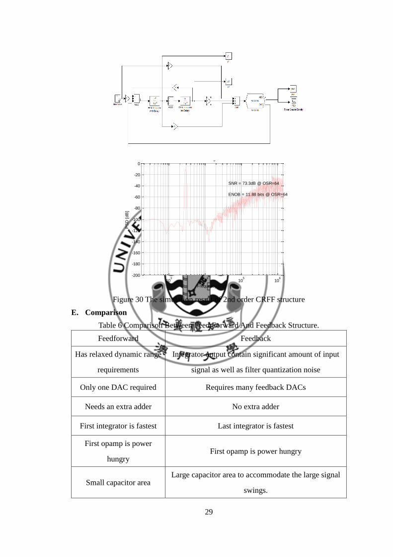
Figure 30 The simulation result of 2nd order CRFF structure
E. Comparison
Table 6 Comparison Between Feed Forward And Feedback Structure.
Feedforward Feedback
Has relaxed dynamic range
requirements
Integrator output contain significant amount of input
signal as well as filter quantization noise
Only one DAC required Requires many feedback DACs
Needs an extra adder No extra adder
First integrator is fastest Last integrator is fastest
First opamp is power
hungry First opamp is power hungry
Small capacitor area Large capacitor area to accommodate the large signal
swings.
103
104
105
106
-200
-180
-160
-140
-120
-100
-80
-60
-40
-20
0PSD of a 2nd-Order Sigma-Delta Modulator
Frequency [Hz]
PS
D [
dB
]
SNR = 73.3dB @ OSR=64
ENOB = 11.88 bits @ OSR=64

30
Advantages of Feedforward compared to Feedback: Lower signal swing at the output
of the integrators (beneficial for amplifier design), larger first loop filter coefficient
(better noise suppression than feedback structure), single DAC only, and depending on
the implementation the feedforward structure might recover from instability without
additional circuitry. The disadvantage of the feedforward structure is that the extra
summing node in front of the quantizer should be very accuracy.
In general, I think that the lower signal swing is the main motivation why feedforward
structures are preferred nowadays. But in this project feedback structure is chosen for
the simple adder.
4.3 Multi-Stage Modulation
The world of noise-shaping converters can be roughly divided into single-bit single-
loop low-order designs, single-bit single-loop high-order designs, multi-loop cascaded
designs with feed-forward error cancellation, and multi-bit noise shapers. In this report,
the multi bit will be not mentioned.
A. The Leslie-Singh (L-0 Cascade) Structure
A simple two-stage delta-sigma ADC contains an L-th order delta-sigma modulator as
its first stage, and a static (i.e., zero-order) ADC as its second stage. The outputs of the
two stages, v1 and v2 are digitally filtered and combined to obtain the overall output v.
ADC
QV
L0
L1
Loop
Filter
H1
H2
E1
E1
E2 V2
V1Y1
Figure 31 The L-0 cascade (Leslie-Singh) structure
As shown, the quantization error e1 (n) of the input stage is extracted in analog form by
subtracting the input signal y1 of the internal quantizer from its output v1.

31
𝑉(𝑧) = 𝑉1(𝑧)𝐻1(𝑧) − 𝑉2(𝑧)𝐻2(𝑧) (41)
Usually H1 implements the latency of the second ADC:
𝐻1 = 𝑧−𝑘
V(z) = z−k[STF1(z)U(z) + NTF1(z)E1(z)] − NTF1(z){z−k[E1(z) +
E2(z)]}
= z−k[STF1(z)U(z) − NTF1(z)E2(z)] (42)
Comparing the output V (z) with the first-stage output V1 (z). NTF1 shapes now the q-
error of the second stage, which can be made much smaller than the q-error of the first
stage because the second stage has no feedback, no delay issues and it can be
implemented as multi-bit such as pipeline ADC which is easier than a multi-bit loop
quantizer in the first stage. Hence, this technique can enhance the SQNR by as much as
25~30 dB.
Figure 32 Simulation result of the 2-0 cascade (Leslie-Singh) structure
Further, to avoid the subtraction altogether, the input signal of the second stage can be
chosen as y1 (n), the input signal of the first-stage ADC, instead of e1 (n).
103
104
105
106
-200
-180
-160
-140
-120
-100
-80
-60
-40
-20
0PSD of a 2nd-Order Sigma-Delta Modulator
Frequency [Hz]
PS
D [
dB
]
SNR = 71.2dB @ OSR=64
ENOB = 11.53 bits @ OSR=64

32
ADC
QV
L0
L1
Loop
Filter
H1
H2
E1
E1
E2 V2
U Y1V1
Figure 33 The L-0 cascade (Leslie-Singh) structure
𝑌1(𝑧) = 𝑉1(𝑧) − 𝐸1(𝑧) (43)
Keeping the H1=z-k but choosing 𝐻2(𝑧) =𝑁𝑇𝐹1(𝑧)
𝑁𝑇𝐹1(𝑧)−1
Finally,
V(z) =z−kSTF1(z)
1−NTF1(z)U(z) +
z−kNTF1(z)
1−NTF1(z)E2(z) (44)
In signal band, |NTF1|<<1, and hence the SQNR obtained with the new V (z) is very
close to the one obtained with the V (z) mentioned before.
A disadvantage is that y1 (n) contains the signal u (n) as well. Hence, the second ADC
must be able to handle much larger signals and must have a much higher linearity!
B. MASH Modulator
An obvious extension of the Leslie-Singh modulator, which historically preceded it, is
the cascade modulator, also called multi-stage or MASH (for Multi-stage noise-Shaping)
modulator. Here, the second stage is realized by another delta-sigma modulator.
QL0
L1
Loop
Filter
H1
H2
E1
E1
E2 V2
V1Y1
Q
L0
L1
Loop
Filter2
V
Figure 34 A MASH structure
As Figure 34 shown, e1 (the quantization error) of the input stage is found in analog
form by minus the input to its internal quantizer from its output.

33
V1(z) = STF1(z)U(z) + NTF1(z)E1(z) (45)
𝑉2(𝑧) = 𝑆𝑇𝐹2(𝑧)𝑈(𝑧) + 𝑁𝑇𝐹2(𝑧)𝐸2(𝑧) (46)
Moreover,
𝑉(𝑧) = 𝑉1(𝑧)𝐻1(𝑧) − 𝑉2(𝑧)𝐻2(𝑧) (47)
To cancel the E1 (z), it is required that
𝐻1(𝑧)𝑁𝑇𝐹1(𝑧) = 𝐻2(𝑧)𝑆𝑇𝐹2(𝑧) (48)
The overall output,
𝑉(𝑧) = 𝑆𝑇𝐹1(𝑧)𝑆𝑇𝐹2(𝑧)𝑈(𝑧) − 𝑁𝑇𝐹1(𝑧)𝑁𝑇𝐹2(𝑧)𝐸2(𝑧) (49)
A typical case is a MASH with two 2nd -order modulators (2-2 MASH)
STF1(z) = STF2(z) = z−2 (50)
NTF1(z) = NTF2(z) = (1 − z−1)2 (51)
V(z) = z−4U(z) − (1 − z−1)4E2(z) (52)
Noise shaping performance of a 4th -order single-loop modulator, but stability of a 2nd
-order modulator.
Here are some simulation results of different MASH structure.
Figure 35 Simulation result of the 1-1 MASH structure
103
104
105
106
-200
-180
-160
-140
-120
-100
-80
-60
-40
-20
0PSD of a 2nd-Order Sigma-Delta Modulator
Frequency [Hz]
PS
D [
dB
]
SNR = 75.1dB @ OSR=64
ENOB = 12.18 bits @ OSR=64

34
Figure 36 Simulation result of the 2-1 MASH structure
As the order of first stage increases, the SNDR performance is better. Further, the 3-
stage and 4-stage structure
Figure 37 Simulation result of the 1-1-1 MASH structure
As shown, the SNDR performance as well as the stability performance of 3-stage (1-1-
1) MASH is better than 3-stage (2-1).
103
104
105
106
-200
-180
-160
-140
-120
-100
-80
-60
-40
-20
0PSD of a 2nd-Order Sigma-Delta Modulator
Frequency [Hz]
PS
D [
dB
]
SNR = 88.6dB @ OSR=64
ENOB = 14.42 bits @ OSR=64
103
104
105
106
-200
-180
-160
-140
-120
-100
-80
-60
-40
-20
0PSD of a 2nd-Order Sigma-Delta Modulator
Frequency [Hz]
PS
D [
dB
]
SNR = 93.6dB @ OSR=64
ENOB = 15.26 bits @ OSR=64

35
Figure 38 Simulation result of the 1-1-1-1 MASH structure
As shown, the SNDR(95 dB) performance is better as the stage increase.
The Multi-loop cascade has the advantages of low-order single-loop single-bit which
are the higher stability. Also it has the higher SNR performance. But the multi-loop
cascade has to near perfect matching between analog integrator and digital differentiator.
It has high requirement in the switching-capacitor circuit.
4.4 Analysis
Single-loop high-order designs are most attractive whenever high SNR, simple circuit
design, and good idle-tone performance are important. The major obstacle to overcome
is the issue of stability. If the SNR is the major requirement, it will be a good choice.
While the Multi-loop cascade has the advantages of low-order single-loop single-bit
and high-order single-loop single-bit which are high SNR as well as the higher stability.
But the multi-loop cascade has to near perfect matching between analog integrator and
digital differentiator. It has high requirement in the switching-capacitor circuit.
Therefore, Single-loop high-order designs is a good choice for the project.
103
104
105
106
-200
-180
-160
-140
-120
-100
-80
-60
-40
-20
0PSD of a 2nd-Order Sigma-Delta Modulator
Frequency [Hz]
PS
D [
dB
]
SNR = 95.0dB @ OSR=64
ENOB = 15.49 bits @ OSR=64

36
Table 7 Comparison Between Single Loop And Multi-Loop Cascode
Modulator
type Advantages Disadvantages
Low-order
single-loop
single-bit
(≤ 3)
• Guaranteed stability
• Simple loop filter
design
• Simple circuit design
• Low SNR (except for high
oversampling ratios)
• More prone to idling tones (dither
may help)
High-order
single-loop
single-bit
• High SNR for modest
oversampling ratios
• Simple circuit design
• Less prone to idling
tones.
• Difficult loop filter design
• Stability is signal dependent
• Maximum input range must be
restricted to ensure stability
Multi-loop
cascade
• High SNR for modest
oversampling ratios
• Stability guaranteed
• Requires near-perfect matching
between analog integrator and
digital differentiator. Complex
switched-capacitor circuits are
required to ensure matching.
• Imperfect matching may result in
leakage of tones into baseband.
• Decimation filter must allow for
must allow for multi-bit inputs.

37
V NOISE ANALYSIS AND BEHAVIOR MODEL
5.1 Noise analysis
After the compared the feedback with feed-forward as well as single loop and multi
loop structure, we decided to use the feed-forward and single loop structure CRFB to
achieve our target SNR=105dB. Where the oversampling ratio is 128 and the quantizer
is 1.5bit. In upper part, the SNR performance of 2nd order single-loop is not enough to
achieve the target even use 4 times OSR=256. Therefore, 3rd order modulation is the
better choice.
Here it shows the performance in the ideal modulation, which has the quantization noise
only, is pretty good as SNR=124.4dB. But in practice, there are many other noise in the
circuit. The main non-idealities of the circuit which will be design in this project are
following:
Operational amplifier nonidealities:[28]
1. Bandwidth of Op-amp;
2. Slew rate of Op-amp;
3. Operational amplifier saturation voltages.
thermal noise(kT/C) of the Switch Capacitor structure;
noise of op-amp;
clock jitter at the input sampler;
Figure 39 3rd order CRFB performance
103
104
105
106
-200
-180
-160
-140
-120
-100
-80
-60
-40
-20
0PSD of a 3nd-Order Sigma-Delta Modulator
Frequency [Hz]
PS
D [
dB
]
SNR = 124.2dB @ OSR=128
ENOB = 20.34 bits @ OSR=128

38
you
t
you
t
y3 y3
y2 y2
y1 y1
kT
/CIN kT
/C n
ois
e1
a3
c1c2
g1
b4
b1
a2
c3
b3
b2
a1
Op
No
ise
Wh
ite
no
ise
z -1
1-z
-1
RE
AL
In
teg
rato
r
(wit
h D
ela
y)2
z -1
1-z
-1
RE
AL
In
teg
rato
r
(wit
h D
ela
y)
1 1-z
-1
RE
AL
In
teg
rato
r
(no
De
lay)
PS
D
Po
we
r S
pe
ctra
l D
en
sity
J
Jitt
ere
d S
ine
Wa
ve
Ad
d5
Ad
d4
Ad
d3
Ad
d2
Ad
d1
AD
C-D
AC
DA
C
AD
C
AD
C-D
AC
Fig
ure
40 T
he
3rd
ord
er C
RF
B w
ith t
he
nois
e blo
ck

39
A. Operational Amplifier Non-idealities
a) Finite DC gain
The dc gain of the integrator in the figure of CRFF is closing to infinite, but in practice
the DC gain can’t be such high. If the dc gain cannot be infinite, the performance of the
dc response of the integrator will decrease so that the total SNR performance will
decrease as the dc gain decrease.[29]
V1
Φ1 Φ2
Φ2
V2
Φ1 VOUT
C1
A0
C2
Φ2
Φ1
nT (n+1)T
Figure 41 Switched capacitor integrator with finite gain op-amp
For ideal case which has infinite gain,
𝑉𝑜𝑢𝑡
𝑉1−𝑧𝑉2= (
𝐶1
𝐶2)
𝑧−1
1−𝑧−1 (53)
It is a non-inverting integrator. And for the finite gain, the transform function become
𝑉𝑜𝑢𝑡
𝑉1−𝑧𝑉2=
𝐶1
𝐶2[
𝐴0
𝐴0+1+𝐶1/𝐶2]
𝑧−1
1−(1+𝐴0)𝐶2
𝐶1+𝐶2+𝐴0𝐶2𝑧−1
(54)
The pole shift from 1 to (1+A0)/ (1+A0+C1/C2). The shift of the pole causes the shift
of the NTF zeroes because of the relationship between them. A second order modulator
can be represented,
NTF ≈ (1 − 𝑧𝑝1 ∙ 𝑧−1)(1 − 𝑧𝑝2 ∙ 𝑧−1) (55)
zp1 and zp2are the zeroes of the NTF cause by the shift.
In the situation that the A0 and capacitances are equal
NTF = (1 − 𝑧−1 𝐴0+1
𝐴0+2)2 (56)

40
Figure 42 NTF of a second order modulator for three different dc gains of the op-
amps.
It (fig 41) shows that only the shaping below a corner frequency fc will be affected by
the finite dc gain. If the signal band is larger than fc, the noise power will not be affect
by the change of the dc gain. And if the signal band is smaller than fc (fig 41), the noise
power will increase as the dc gain of the op-amp decrease. Therefore, the finite dc gain
is one of the non-idealitise which affects the SNR performance.
The fc (corner frequency) can be represented by
𝑒𝑆𝑝𝑇 =𝐴0+1
𝐴0+2 (57)
𝑓𝑐 =𝑓𝑠
2𝜋ln {1 −
1
𝐴0+2} ≈
𝑓𝑠
2𝜋(𝐴0+2) (58)
The SNR performance will not be affected if fB >> fc; therefore if the gain and
oversampling ratio can satisfy π (A0+2)>>OSR, the SNR performance will be better.
Therefore, we decrease the dc gain and see the performance of the whole system so that
we can find a dc gain which is easy to achieve for the op-amp and dose not much affect
the performance.
104
105
106
-200
-180
-160
-140
-120
-100
-80
-60
-40
-20
0PSD of a 2nd-Order Sigma-Delta Modulator
Frequency [Hz]
PS
D [
dB
] 10
100
1000
10000

41
Table 8 The Performance Of System As Gain Decrease
Finite DC gain SNR
80dB 124.2dB
60dB 123.9dB
54dB 123.9dB
52dB 122.5dB
50dB 120.4dB
It must be as it is shown that performance will be worse as DC gain decrease. And
finally we choose the 54dB as the DC gain which is easy to achieve for the op-amp and
dose not much affect the performance.
Figure 43 The system performance With 54dB gain
b) Finite BW and SR
The non-ideal integrator has finite bandwidth and slew rate which are the parameter in
the matlab model of CRFF figure. The effect of the finite bandwidth and the finite slew
rate are related to each other. Furthermore, they may be interpreted as a nonlinear gain.
[28]
The finite op-amp bandwidth and slew-rate cause the settling error
103
104
105
106
-200
-180
-160
-140
-120
-100
-80
-60
-40
-20
0PSD of a 3nd-Order Sigma-Delta Modulator
Frequency [Hz]
PS
D [
dB
]
SNR = 123.9dB @ OSR=128
ENOB = 20.29 bits @ OSR=128

42
Figure 44 Response of a unity gain buffer with finite slew-rate and bandwidth
In Figure 44, it shows that since the integration phase only lasts Ts/2, for a certain
bandwidth if the slew is such small that the signal cannot achieve the high point after
half period. It causes an error. So, it the bandwidth is large enough the SR can set to be
a small value. On the other hand, if the bandwidth is small, it requires a higher SR.
Also, we change the SR and BW to see the performance of the whole system so that we
can find SR and BW which are easy to achieve for the op-amp and dose not much affect
the performance.
The minimum value of the GBW is
GBW = BW ∗ gain = 22.05kHZ ∗ 500 = 11.025MHZ (59)
Table 9 The Performance Of System As Sr And Gbw Change
GBW(MHz) SR(V/us) SNR(dB)
12 100 124.2
12 90 118.8
12 80 112.8
20 80 123.3
30 80 123.9
40 80 124.2
40 70 124.2
40 60 124.2
40 50 124.2
40 40 124.2
40 30 121.8
50 30 124.2

43
Since, the higher GBW is easier to get than the higher SR we finally choose the
GBW=50MHz and SR=30V/us to do the further error simulation and further design.
Figure 45 The system performance with GBW=50MHz and SR=30V/us
c) Saturation voltages
As known, the when the signal excels saturation voltage of the op-amp the extra part of
signal will be banned. For signal conversion, it will cause the distortion some part of
the signal cannot be processed. Therefore the signal power decrease as well as the SNR
performance decrease. In the model as shown in Fig CRFF, the saturation voltage is one
of the parameter of the non-ideal integrator.
We decrease the saturation voltage to find the minimum value which doesn’t cause
distortion.
Figure 46 The output of each integrator with Input amplitude is ±0.5 V
103
104
105
106
-200
-180
-160
-140
-120
-100
-80
-60
-40
-20
0PSD of a 2nd-Order Sigma-Delta Modulator
Frequency [Hz]
PS
D [
dB
]
SNR = 124.2dB @ OSR=128
ENOB = 20.34 bits @ OSR=128
-0.05 0 0.050
50
100
150
200
250First Integrator Output
Voltage [V]
Occurr
ences
-0.4 -0.2 0 0.2 0.40
50
100
150
200
250Second Integrator Output
Voltage [V]
Occurr
ences
-1 -0.5 0 0.5 10
50
100
150
200
250Third Integrator Output
Voltage [V]
Occurr
ences

44
Table 10 The Performance Of System As Saturation Voltage Change
Saturation
voltages(V)
SNR(dB)
±3 124.2
±2.5 124.2
±2 124.2
±1 124.2
±0.8 120.3
±0.6 104.9
Figure 47 The system performance 1V saturation voltage
Here, we can see the saturation voltage of the op-amp should be larger than 1 V which
is hard to achieve. So we will have some modification in the circuit design stage.
B. Thermal and operation amplifier noise-Switches Thermal Noise (kT/C)
In switch capacitor circuit, the random fluctuation of carriers due to thermal energy can
cause the thermal noise which will be present even at equilibrium. Thermal noise has
wide band and a white spectrum, it is only limited by the time constant of the switched
capacitors or the bandwidth of the op-amp. The SC first-order 𝛴𝛥 modulator, as
example, the sampling capacitor Cs is in series with a switch with finite resistance Ron.
And periodically opens cause the sampling noise voltage onto Cs. The total thermal
noise power can be represented by[28]
103
104
105
106
-200
-180
-160
-140
-120
-100
-80
-60
-40
-20
0PSD of a 3nd-Order Sigma-Delta Modulator
Frequency [Hz]
PS
D [
dB
]
SNR = 123.6dB @ OSR=128
ENOB = 20.24 bits @ OSR=128

45
eT2 = ∫
4𝑘𝑇𝑅𝑜𝑛
1+(2𝜋𝑓𝑅𝑜𝑛𝐶𝑠)2 𝑑𝑓∞
0=
kT
Cs∙OSR (60)
Where k is the constant, T is the temperature in k,
From the table X, we can see the thermal noise is much larger than other noise.
Therefore the switch thermal noise will dominate the other noise. And if the Cs is larger,
the power consumption will be higher. Here, we choose Cs=1pF to do further analysis.
Table 11 The Performance Of System As Sampling Capacitance Change
Switches Noise(Cs) SNR(dB)
2.5pF 101.8
2pF 99.9
1.5pF 97.7
1pF 96.6
0.5pF 93.0
Figure 48 The system performance with Cs=1pF
C. Operational Amplifier Noise
In this model we considered only thermal noise, while flicker (1/f) noise and dc offset
are neglected. Through a transistor level noise simulation for the complete integrator in
the proper clock phase which is including feedback, sampling and load capacitors, it
evaluated the noise power 𝑉𝑛2.
103
104
105
106
-200
-180
-160
-140
-120
-100
-80
-60
-40
-20
0PSD of a 3nd-Order Sigma-Delta Modulator
Frequency [Hz]
PS
D [
dB
]
SNR = 96.6dB @ OSR=128
ENOB = 15.76 bits @ OSR=128

46
Table 12 Performance Of System As Input-Referred Operational Amplifier Noise
Change
Input-referred operational amplifier noise(Vn) SNR(dB)
50uVrms 97.7
20uVrms 105.7
10uVrms 111.4
8.3uVrms 112.8
5uVrms 116.6
Figure 49 The system performance with Vn=8.3uV
The 8.3umV is calculated by some approximately method. We use 8.3uV [34] to do
further simulation. But in practice, the operational amplifier noise will be larger.
D. Clock Jitter
The operation of an SC circuit depends on complete charge transfers during each of the
clock phases [39]. Once the analog signal has been sampled, the Switch-Capacitor
circuit is a sampled-data system where variations of the clock period have no direct
effect on the circuit performance. Therefore, the effect of clock jitter on an SC circuit is
completely described by computing its effect on the input sampling signal. This also
means the structure and order of the 𝛴𝛥 modulator will not is not the factor of the
103
104
105
106
-200
-180
-160
-140
-120
-100
-80
-60
-40
-20
0PSD of a 3nd-Order Sigma-Delta Modulator
Frequency [Hz]
PS
D [
dB
]
SNR = 112.8dB @ OSR=128
ENOB = 18.44 bits @ OSR=128

47
effect of the clock jitter on a sigma delta modulator.
For sampled system, the SNR limitations due to jitter can be determined by the
following equation [9];
SNR = −20log (2π𝑓𝑎𝑛𝑎𝑙𝑜𝑔𝑡𝑗𝑖𝑡𝑡𝑒𝑟) (61)
Where f is the analog input frequency, t is the jitter.
Therefore, given a frequency of operation and an SNR requirement, the clock jitter
requirement can be determined as follows.
𝑡𝑗𝑖𝑡𝑡𝑒𝑟 =10
−𝑆𝑁𝑅20
2𝜋𝑓𝑎𝑛𝑎𝑙𝑜𝑔= 34𝑝𝑠 (62)
SNR=124dB and input amplitude is 0.5V.
Table 13 The Performance Of System As Sampling Jitter Change
Sampling Jitter(∆𝝉) SNR(dB)
34𝑝𝑠 124.2
68𝑝𝑠 124.2
100𝑝𝑠 123.4
150𝑝𝑠 122.5
200𝑝𝑠 121.5
250𝑝𝑠 120.7
300𝑝𝑠 119.0
Nowadays, the ∆𝜏 = 34𝑝𝑠 is a relax requirement.
E. Overall noise
Table 14 System Performance With Different Noise
Sigma-delta Parameter SNR(dB)
Ideal modulation 124.2
Finite DC gain
(H=500=54dB)
123.9
Finite
bandwidth(GBW=50MHz)
124.2
Finite Slew-rate
(SR=30V/us)
124.2

48
Saturation voltages
(|Vmax|=3.3V)
123.6
Sampling Jitter (Δ𝝉 =
𝟐𝟎𝟎𝒑𝒔)
124.2
Switch (kT/C) noise
(Cs=1pF)
96.6
Input-referred operational
amplifier noise
(Vn=8.3uV)
112.8
Including all of the non-
idealities
95-96.5
As the table above, all of the noise are considered. And the final result is a range because
of the random noise in the model.
Figure 50 The system performance
kT/C plus
Op-amp thermal noise(75%)
Quantization noise(5%)
Other noise(20%)
Figure 51 Noise budget
In this part, the noise budget of the system is shown (fig 48). The kT/C and op-amp
thermal noise are effecting the performance of the system mostly while the quantization
noise just effect the performance a little bit. Therefore, the decrease the kT/C and op-
amp thermal noise will be the key work to increase the SNR performance of the system.
103
104
105
106
-200
-180
-160
-140
-120
-100
-80
-60
-40
-20
0PSD of a 3nd-Order Sigma-Delta Modulator
Frequency [Hz]
PS
D [
dB
]
SNR = 95.9dB @ OSR=128
ENOB = 15.64 bits @ OSR=128

49
Moreover the preliminary design doesn’t achieve the target, the further decision can be
made.
5.2 Behavioral model
According to the analysis and comparison result, the further decision is using CRFB
structure with OSR=256 and 1.5bit quantizer. Moreover, repeating the analysis above
can get the behavior model of the system
Table 15 Behavior Model Of The Project
Sigma-delta Parameter SNR(dB)
Ideal modulation 134.8
Finite DC gain (G=58dB, 58dB, 50dB) 130.6
Finite bandwidth(GBW=100MHz) 134.8
Finite Slew-rate (SR=60V/us) 134.8
Saturation voltages (|Vmax|=1V) 134.8
Sampling Jitter (Δ𝝉 = 𝟏𝟕𝒑𝒔) 130.7
Switch (kT/C) noise (Cs=10pF) 110.4
Input-referred operational amplifier noise (Vn=1.5uV) 108
Including all of the non-idealities 107-107.5
The swing is acceptable for the output of integrator. Moreover, the SNR performance
can achieve the setting target SNR=105dB.
b2b1
c1 c2 c3
DAC
b3 b4
-a1 -a2 -a3
-g1
v(n)y(n)
u(n)
1
1Z 1
Z
Z
1
1Z
Figure 52 3rd order CRFB architecture

50
Figure 53 The output swing of each integrator with Input amplitude is ±0.4 V
Figure 54 the system performance
Figure 55 The 3rd order CRFB with noise block in matlab
-0.05 0 0.050
20
40
60
80
100
120
140First Integrator Output
Voltage [V]
Occurr
ences
-0.5 0 0.50
20
40
60
80
100
120Second Integrator Output
Voltage [V]
Occurr
ences
-1 0 10
10
20
30
40
50
60
70
80
90Third Integrator Output
Voltage [V]
Occurr
ences
104
105
106
-200
-180
-160
-140
-120
-100
-80
-60
-40
-20
0PSD of a 2nd-Order Sigma-Delta Modulator
Frequency [Hz]
PS
D [
dB
]
SNR = 107.0dB @ OSR=256
ENOB = 17.48 bits @ OSR=256
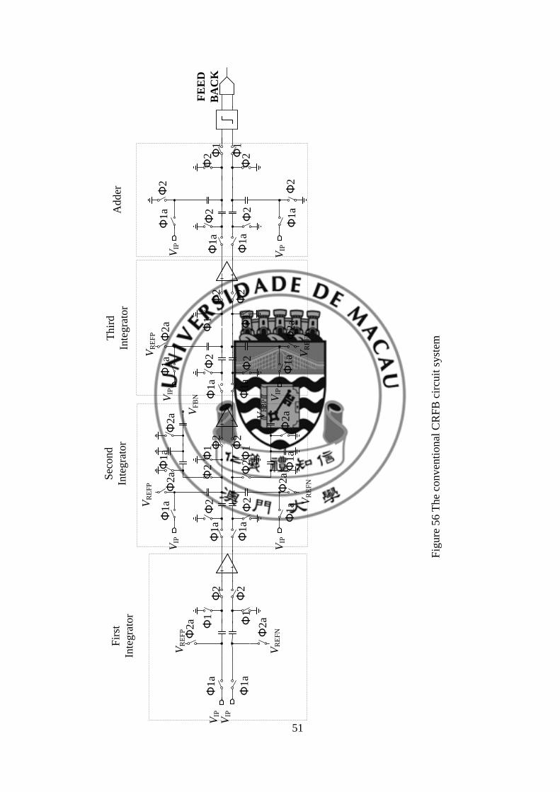
51
Φ1a
Φ1 Φ
2
Φ2
Φ1a
Φ1
VIP
Φ1a
VIP
Φ2a
FE
ED
BA
CK
VR
EF
P
Φ1a
Φ2a
VR
EF
N
Φ2
Φ2
Φ1a
Φ1
Φ2
Φ2
Φ1a
Φ1
VIP
Φ1a
VIP
Φ2a
VR
EF
P
Φ1a
Φ2a
VR
EF
N
Φ2
Φ2
Φ1a
Φ2 Φ
1
Φ1
Φ1a
Φ2
VIP
Φ1a
VIP
Φ2
Φ1a
Φ2
Φ2
Φ2
Φ2Φ
1a
Φ2a V
FB
N
Φ1a
Φ2aV
FB
P
Φ1a
Φ1
Φ2
Φ2
Φ1a
Φ1
Φ2a
VR
EF
P Φ2a
VR
EF
N
VIP
VIP
Fir
st
Inte
gra
tor
Sec
ond
Inte
gra
tor
Thir
d
Inte
gra
tor
Adder
Φ2
Fig
ure
56 T
he
conv
enti
onal
CR
FB
cir
cuit
syst
em

52
VI CIRCUIT DESIGN
For the system, it mainly include clock generator, adder, quantizer and three integrators.
In this project, special integrator called Charge-Pump integrator is used as the first
integrator which is the most power hungry one.
6.1 Charge Pump Integrator
As upper mention, in order to get high resolution system, large OSR and large sampling
capacitor are require to reduce the thermal noise which constraints the power
consumption of op-amp. Moreover, one of the main constraints of the chosen structure
CRFB is the high requirement of first op-amp which requires high DC gain as well as
high power consumption. In this project, a special integrator called charge-pump
integrator shown in above figure is used to improve the power efficiency.[30]
VIN
Φ1 Φ2
Φ2
VREF
Φ1
VOUT
Cs
Ci
(a)
VINVOUT
Φ2 Φ2
Φ1
Φ1Φ2
Cs1=Cs/2
Cs2=Cs/2
Ci2
(b)
Figure 57 (a) Conventional Switch capacitor integrator and (b) charge pump integrator
The figure above (a) shows the normal SC (switch capacitor) integrator. During Φ1, the
input signal is sampling into the sampling capacitor Cs. During Φ2, the sampling
capacitor Cs will connect to the virtual ground and reference voltage feedback from the
DAC to integrate (Vin – Vref). At that time the charge sampled in the sampling capacitor
in Φ1 will transform into Ci. For charge pump integrator shown in fig (b), during
sampling phase Φ1, two sampling capacitor Cs1=Cs2=Cs/2 with sample the input signal

53
same as the conventional one, during Φ2, this two sampling capacitor will connect
together between the virtual ground and the reference voltage feedback from the DAC.
As figure (c) and (d) shown, during Φ2 the sampling capacitor will become Cs/4, but
the signal in it is double, therefore it needs a double of reference voltage to integrate
2(Vin-Vref) by using Ci2=Ci/2.
VOUT
Vref
Cs
Cl
(a)
VOUT
Cs/4
Cs/2k
2Vref
Cl
(b)
Figure 58 (c) Conventional Switch capacitor integrator and (d) charge pump integrator
during Φ2(integration phase)
Power Consumption of Charge Pump Integrator
For a typical op-amp, the gm (transconductance) of the input differential pair is
proportional to the power of the whole op-amp.
𝑃𝑂𝑊𝑂𝑃 ∝ 𝑔𝑚 (63)
The transconductance of the op-amp with sampling rate and settling time required is
given by [30]
𝑔𝑚 =𝜔−3𝑑𝐵𝐶𝐿
𝛽 (64)
Where 𝜔−3𝑑𝐵 𝑖𝑠 the -3dB frequency, β is is the feedback factor the CL is the
capacitance loading.
From figure (c) and (d) ignore the parasitic capacitor, the CL and β for normal integrator
is given by
𝐶𝐿 =𝐶𝑠
𝑘+1+ 𝐶𝑙 (65)
54
𝛽 =1
𝑘+1 (66)
For the CP integrator
𝐶𝐿′ =𝐶𝑠/2
𝑘+2+ 𝐶𝑙 (67)
𝛽′ =2
𝑘+2 (68)
The effective closed-loop load capacitance 𝐶𝐿/𝛽 of both situation is given by
𝐶𝐿
𝛽= 𝐶𝑠 + 𝐶𝑙(𝑘 + 1) (69)
(𝐶𝐿
𝛽)′ =
𝐶𝑠
4+ 𝐶𝑙(
𝑘
2+ 1) (70)
Generally, k is smaller than 1 and Cs>Cl. Therefore(𝐶𝐿
𝛽)
′
≈𝐶𝐿
4𝛽, the thermal noise
analysis shows CP integrator has same input-referred thermal noise as the normal one
[30]. In the sampling phase, the thermal noise of CP integrator and conventional
integrator are the same. During Φ2, since the connection of Cs1 and Cs2, the sample
noise of the CP integrator will be four times of conventional one. But in this period the
signal in the Cs1 and Cs2 is double of the input as well as the reference voltage. Hence,
in the same requirement of settling time, thermal noise performance as well as the
sampling rate for this two kind of integrator:
𝑔𝑚′ =
𝑔𝑚
4 (71)
Which will correspond to the reduction of the power consumption by about four time.
𝑃𝑂𝑊𝑜𝑝′ =
𝑃𝑂𝑊𝑂𝑃
4 (72)
As a conclusion, charge pump integrator is a good choice for this project.

55
VIP
Φ1
aΦ
1
Φ1
a2
VR
EF
P
Φ1
Φ2
aΦ
2
VIN
Φ1
aΦ
1
Φ1
a
2V
RE
FN
Φ1
Φ2
aΦ
2
Φ1
aΦ
1 Φ2
Φ2
Φ1
aΦ
1
VIP
Φ1
a
VIP
Φ2
a
FE
ED
BA
CK
VR
EF
P
Φ1
aΦ
2a
VR
EF
N
Φ2
Φ2
Φ1
aΦ
1Φ
2
Φ2
Φ1
aΦ
1
VIP
Φ1
a
VIP
Φ2
a
VR
EF
P
Φ1
aΦ
2a
VR
EF
N
Φ2
Φ2
Φ1
aΦ
2 Φ1
Φ1
Φ1
aΦ
2
VIP
Φ1
a
VIP
Φ2
Φ1
aΦ
2
Φ2
Φ2
Φ2Φ
1a
Φ2
a VF
BN
Φ1
aΦ
2aV
FB
P
Fir
st
Inte
gra
tor
(CP
)
Sec
on
d
Inte
gra
tor
Th
ird
Inte
gra
tor
Ad
der
Φ2
Fig
ure
59 T
he
CR
FB
cir
cuit
syst
em w
ith C
P i
nte
gra
tor

56
6.2 Op-Amp Design
For a normal sigma delta ADC with a large OSR, the first order loop will dominates no
matter the performance as well as the power consumption. The power of the first Op-
amp depends on the thermal noise, sampling rate and settling time. Therefore the first
integrator is one of the key parts in the system. Repeat the procedure to find the new
requirement of the first op-amp. For the normal simulation in matlab, the requirement
gain of the first op-amp is 58dB
Table 16 New Gian Requirement Of First Op-Amp
The gain of first Op-amp(dB) simulation result of Cadence(dB)
54 133
50 133
48 133
46 132
42 130
Using the new technique, the require gain of the first integrator is reduce from 58dB to
48dB almost 4 times reduction.
VDD
GND
VIPVIN
VCMFB
VB1
vOPvON
M2 M3
M4
M6
M5
M7
M8 M9
M10 M11
M1VB4
VB2
VB3
M12
M14
M13
M15
VCMFB1
vOP1vON1
vOP1 vON
vON1 vOP
C1R1
Figure 60 First op-amp structure
In order to fulfill the requirement of the first op-amp especial gain, GBW, SR and the
swing, 2 stage op-amp using folded-cascode is chosen. Using folded-cascode with as
first stage can get a high gain, and the common source amplifier can give the remaining
gain and large output swing for the op-amp. And since the reference voltage of the CP

57
integrator is double, the input deferential pair of the op-amp must be NMOS. If here
using PMOS, the input differential pair can’t be saturated. To implement GBW and
phase margin requirement, miller compensation is needed.
For the miller compensation,
Figure 61 The feedback test circuit
𝑍1 =𝑍𝐹
1−𝐴 𝑎𝑛𝑑 𝑍2 =
𝑍𝐹
1−1
𝐴
For capacitor,
𝐶1 = 𝐶(1 + 𝐴) 𝑎𝑛𝑑 𝐶2 = 𝐶 (1 +1
𝐴) (73)
Where A is negative number. Therefore, a smaller capacitor is used to compensate the
amplifier. And here CC is the miller capacitor which is used to separate the main pole
and the side poles that one of the poles is leading to other that can decrease the GBW.
Moreover, the R is a nulling resistor which can let the zeros at the right plane move to
left plane thus the phase margin will be stable and increase.
C1 C2 C3 C4
Φ1Φ2 Φ2 Φ1
Φ1 Φ2 Φ2 Φ1
VCM
VCMFB
VBIAS VBIAS
VCM
VOP VON
Figure 62 The common mode feedback structure
In order to stabilize the output common mode voltage, the switch- capacitor common
mode feedback circuit is used. In general, a common mode feedback circuit consists of
a common detect circuit and a comparison amplifier.[14] The difference between output

58
voltage of the CMFB circuit and the output of the op-amp is similar to the difference
between Vbias and Vcm.
VDD
GND
IREF
VREF
1
VB0
VREFP
2 3
VB34
VREFP VREFP
VB1 VB25 6
VB2
7
Figure 63 The baising circuit
Build the biasing circuit basic on the current mirror theorem.[35]
Table 17 1st op-amp performance
Requirement 1st op-amp
Gain 48dB 58dB
GBW(Hz) 100M 231M
SR(V/us) 60 120
For second op-amp, the requirement is more relax than the first one except the gain.
Here a 1 stage folded-cascode with gain boosting [10] is used. Since the PMOS
differential pair for folded-cascode architecture allows low common voltage, in second
order the input common voltage is 500mV. Besides, the PMOS input pair can supply a
large overdrive voltage which can relaxes the design of the switch.

59
VDD
GND
VIPVIN
VCMFB VB2VB2
VB1
VB4
VB3 VB3
vOPvONM1
M2 M3
M4
M8
M12
M6
M10
M7
M11
M5
M9
M13
M14 M15
M18 M19
M16 M17
Figure 64 Second op-amp structure
Table 18 2nd Op-Amp Performance
Requirement 1st op-amp
Gain 58dB 62dB
GBW(Hz) 100M 332M
SR(V/us) 60 115
VDD
GND
VIPVIN
VCMFB
VB1
vOPvONM2 M3
M4
M6
M5
M7
M8 M9
M10 M11
M1
VB4
VB2
VB3
M12
M14
M13
M15
VCMFB1
vOP1vON1
Figure 65 Second op-amp structure

60
Table 19 3rd Op-Amp Performance
Requirement 1st op-amp
Gain 50dB 51dB
GBW(Hz) 100M 187M
SR(V/us) 60 110
For third integrator, the output swing is as large as ±300mV, it is hard to build 1 stage
op-amp with ±300mV swing to get a high gain when full scare is 1V. Therefore, 2
stage architecture is needed.
6.3 Zero Optimization
For the CRFB structure, it needs a local feedback from third integrator output to second
integrator input to make up a resonator which effects the zero. However, the local
feedback coefficient is very small generally. For example, in this project this local
feedback coefficient is g=-9.03*10^-5 corresponding to a Cb=9a, it need a very small
capacitor which is impractical small to implement this coefficient.
Φ1a
Φ1 Φ2a Φ2
Φ2 C1C2
C3
Vo3Vi2
Figure 66 The SC local feedback
Therefore, a switch capacitor circuit [47] shown above figure 64 is used to implement
the local feedback instead of a single capacitor in this project.
During Φ1, C1, C2 and C3 will sample the signal from V3. But only the charge in C2 is
transform to the second integrator in Φ2. According to that, a series suitable capacitor
can replace the impractical small capacitor. It needs charge in C2 is same as the Cb.
Q = g ∙ V𝑜3
The charge in C2 and C3 is given by
Q2 = V𝑜3𝐶1||(𝐶2+𝐶3)
2∙
𝐶2
𝐶3+𝐶2 (74)
Q2 = Q
Set up two of them, can get the other one.

61
6.4 1.5 bit quantizer
The 3-level-quantizer can be implemented from the simple comparator.
The Figure 67 Comparator schematic diagram shows the comparator schematic [12].
The dimension of the transistors we used is small, actually because of the bandwidth
and speed’s low requirement. It includes two input transistors (M2, M3), and one clock
transistor (M1).
The comparator works differently during two phases, when the CLK fails, precharge
transistors M8 and M9 (also M10 and M11) are turning on, so the outputs of comparator
are reset to Vdd. In another phase, when CLK starts to rise, the tail current (M1) of the
differential pair is turned on, the voltage at output nodes fails with a fast rate, and the
voltage imbalance is created.
VDD
VSS
M7
vIN
M6
M5M4
M8 M9M10 M11
M2 M3
M1
vIP
vOP
vON
CLK CLK
CLK
Figure 67 Comparator schematic diagram
In the system, for the reason of eliminate the comparator kickback, the comparator
regenerates between Φ1 and Φ2, so the settling transients are not disturbed. Furthermore,
an RS flip-flop can be used to keep the output during the hold period.
R
S
Q
Q’
vOP
vON
output
Figure 68 RS flip-flop
By checking the truth table of SR-latch in Table 20. If Vop is applied to R, and Von

62
is applied to S, the condition is perfectly matched, and the output can be hold without
any other disturbance.
Table 20 Comparison Of SR-Latch And Comparator
SR latch operation Comparator
Characteristic table Characteristic table
S R Q next Action Vop Von output action
0 0 Q Hold state 0 0 X Not allowed
0 1 0 reset 0 1 0 reset
1 0 1 set 1 0 1 set
1 1 X Not allowed 1 1 1 Hold state
In this system, a 1.5bit quantizer is used to get a higher SNDR. The circuit of the circuit
is shown in Figure 69 . Two comparators are used to generate two digits, here D0
indicates the higher digit and D1 indicates the lower digit.
C1
C2
VCMVREFP
VCMVREFN
VIP
VIN
Φ1
Φ2
Φ1
Φ2
Φ2Φ2
C1
C2
VCMVREFN
VCMVREFP
VIP
VIN
Φ1
Φ2
Φ1
Φ2
Φ2Φ2
CLK
D0
D1
Figure 69 3-level-quantizer schematic
The switched-capacitor architecture is to make the comparison between the input
voltage and the two reference voltages. For the Vcm=500mV, and also considering the
swing of the input voltage, the reference voltages are set as Vrefp=600mV and

63
Vrefn=400mV.
6.5 Clock Generator
As we known, a number of clock phases that are obtained from a master clock. For
example, the delay, overlapping or non-overlapping specific features are needed for our
design.
The figure below shows a structure which generates four scheduled phases from one
preliminary phase, mainly controlled by the cross-coupled flip-flop, [38]
CLKΦ1
Φ2
Φ3
Φ4
Figure 70 The clock generation logic
In that Figure 70, all the logic gates in the square frame are settled as 1ns delay, when
the input phase goes from 1 to 0, for Φ2, there is a delay of four inverters after the input
phase. For Φ1, observing that one input of output NAND gate is from the output of first
inverter, following this, it’ll decreases after 2 delay time. So the falling edge of Φ1 is 2-
delay-time before the Φ2. Following this, Φ3 and Φ4 are also transformed into non-
overlapping phases at the output nodes.
For the first input clock, the period is calculated from the system’s requirement. The
bandwidth is 20 kHz, and the OSR is 256, so the sampling frequency is
2*bandwidth*OSR= 10.24e6 Hz.
6.6 Feedback Logic
The feedback signal can also be implemented by logic gates, the 1.5 bit quantizer gives

64
the output signal D0 and D1, here D0 indicates the higher digit and D1 indicates the
lower digit. The feedback controls the transfer of data, so that the analog architecture is
configured.
A1CLK
CLK
CLK
B1
C1
D0
D1
Figure 71 The feedback circuit
Referring to the system, it has three different feedback voltages, Vdd is given to A1,
and also Vcm defined as B1, Vgnd as C1. Noticing all the three outputs are connected
with an NAND gate which has a ‘CLK’ input, the feedback logic only works when the
working phase equals to one during the hold period. The truth table is:
Table 21 The Feedback Logic
A1 B1 C1
D0=0; D1=0 1 0 0
D0=0; D1=1 0 1 0
D0=1; D1=0 1 0 1
D0=1; D1=1 0 0 1
The Table 21 shows that when output is low (D0=0; D1=1), the feedback voltage is high
(A1=Vdd). In opposite, when output is high (D0=1; D1=1), the feedback voltage is low
(C1=Vgnd). When’ D0=0; D1=1’, the output is connected with B1=Vcm.
As a reminder, here ‘D0=1; D1=0’ is not possible as D0 and D1 are from the 3-level-
quantizer output.
6.7 Switches Replacing
For discrete-time sigma-delta ADC, the sample and hold circuit is typically used at the
front of each stage. With the requirement of high speed and linearity, sampling switch

65
should maintain the ability of transfer the signals precisely. Also for different parts in
the ADC, unlike types of switches are needed.[35]
MOSFET Switch
So from figure it is a simple sampling circuit, it includes a switch and a capacitor.it
works because (a) when passing current is zero, the switch can also be turned on. (b)
When turning on, no matter how the voltage of bulk changes, it doesn’t affect the
voltage of drain and source.
Vin
CH
CLK
Figure 72 MOSFET as a switch
From the simulation, the switch is bidirectional. So when CLK goes high, the circuit
can track the input signal, and if CLK goes low, the capacitor can hold the signal until
the next period.
CMOS Switch
CMOS switch can also be called transmission gate. It is often used when very large or
small voltage input, under such situation, the transmission resistor will change critically,
and will cause certain distortion. [35]
Vin Vout
CH
Ron,p Ron,n
Ron,eq
VTHP VDD-VTH
VIN
CLK
CLK’
Figure 73 The transmission gate
So why it is reasonable to use switch when the rail-to-rail voltage transferred, the shows
that the equivalent resistant is much stable than the single transistor switch. Moreover,
to avoid uncertainty of the sampling, NMOS and PMOS switch should turn on or off at
the same time
Bootstrapped Switch
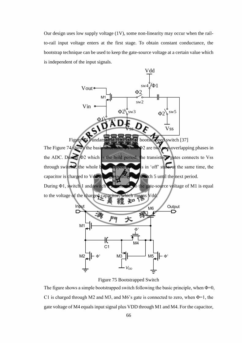
66
Our design uses low supply voltage (1V), some non-linearity may occur when the rail-
to-rail input voltage enters at the first stage. To obtain constant conductance, the
bootstrap technique can be used to keep the gate-source voltage at a certain value which
is independent of the input signals.
M1
sw1
Vss Vss
Vdd
sw3
sw2
sw5
sw4
Vin
Vout
Φ1
Φ1
Φ2 Φ2
Φ2
Figure 74 Fundamental principle of bootstrapped switch [37]
The Figure 74 shows the basic structure, Φ1 and Φ2 are two non-overlapping phases in
the ADC. During Φ2 which is the hold period, the transistor’s gates connects to Vss
through switch2, the whole bootstrapped switch is in ‘off’ state, at the same time, the
capacitor is charged to Vdd through switch4 and switch 5 until the next period.
During Φ1, switch 1 and switch 2 are closed, so the gate-source voltage of M1 is equal
to the voltage of the charged capacitor, which means Vdd.
Input Output
M1
M2 M3
C1
M5
M4
M6
VDD
Φ’ Φ’
Φ’
Figure 75 Bootstrapped Switch
The figure shows a simple bootstrapped switch following the basic principle, when Φ=0,
C1 is charged through M2 and M3, and M6’s gate is connected to zero, when Φ=1, the
gate voltage of M4 equals input signal plus VDD through M1 and M4. For the capacitor,

67
it should not too large because we need a fast rate to store and release the charge, we
set it as 300f F.
M1
M2
Input
Output
M3 M4
M5
M6 M7 M8
C1 C2C0
Vdd
Vss
Figure 76 Bootstrapped switch with implementation
During the simulation, it is still found that the simple bootstrapped switch still cannot
fulfill the target performance, for Figure 76, an implemented switch is introduced.
The improvement focus on the M2 and M6, as we can see, M2 functions as an input
switch, which is also bootstrapped.
For M6, because the switch4 may leak when the bootstrap capacitor is charged to a
voltage level exceeding Vdd. Differ from the formal case, the switch4, a NMOS is used
to replace the PMOS switch. Plus, a charge-pump voltage shifter is built by M7, M8,
C1, C2, so a clock level between Vdd to 2Vdd can be used to control the NMOS M6.
As a supplement, for switch distortion analysis [16], we know the one main part from
the Charge injection. However, because we use bootstrap, Vgs is a constant value, so
the error voltage is signal independent, also for the reason of differential input, this error
will be finally be cancelled. For the Clock feed-through problem, its value also doesn't
affect the final performance. Actually the main noise comes from the thermal noise, so
in this report we won’t talk in details.
VII PERFORMANCE
The output waveform as well as the PSD for the 3 order CRFB sigma delta analog to
digital converter with charge pump integrator is shown below. It clearly shows the input

68
signal and the noise most of which is shifted to the high frequency band (>20kHz) that
will be filter by a low-pass filter. And the in-band (<20kHz) noise level is very low
about -110dB. A zero locates at about 15kHz. The total Signal-to-Noise-Distortion
Ratio is 106dB. The digital signal output is shown in figure 78. Moreover, Figure 79
the gives the SNDR performance versus different input amplitude. The corresponding
dynamic range is 107dB.
Figure 77 Output PSD for the system
Figure 78 Output waveform
103
104
105
106
107
-140
-120
-100
-80
-60
-40
-20
0
Frequency(Hz)
PS
D(d
B)
PdydB

69
Figure 79 Measured SNDR versus input amplitude
Power consumption
For the whole system, the power mainly drive by the op-amps. It can be seen from the
table 22 that the first op-amp costs the half of the total power even using the charge
pump technique.
Figure-of-merit (FOM) is a character of the system to indicate the relationship between
power consumption and the SNDR as well as bandwidth of the system. In other word,
it is a efficiency indicator of the system. FOM is defined as
FOM =𝑃𝑜𝑤𝑒𝑟
2∙𝐵𝑊∙2(𝑆𝑁𝐷𝑅(𝑑𝐵)−1.76)/6.02 (75)
Also, a normal CRFB system is built. The comparison of the system using CP integrator
and the conventional one is shown in Table 23. It is seen that with the similar
performance, the system using CP integrator as first integrator cost less power than the
system using conventional one. It saves around % power by using CP integrator.
Table 22 Power Consumption For Each Part
part power
1st Op-amp 673uW
2nd Op-amp 338uW
y = 0.98 x + 105.20
0
20
40
60
80
100
120
-140 -120 -100 -80 -60 -40 -20 0
SN
DR
(dB
)
Input(dBFS)

70
3rd Op-amp 321uW
comparator 2*0.02uW
total 1.332mW
FOM 204f
Table 23 Comparison Of CP And Conventional
CP Conventional
Technology 65nmCMOS 65nmCMOS
Sampling Frequency 10.24MHz 10.24MHz
Bandwidth 20kHz 20kHz
Peak SNDR 106dB 102dB
Power consumption 1.332mW 1.972mW
FOM 204f/conv. 479f/conv.
Besides, the comparison of this work and other work with similar input range (≤1.1),
OSR (>100) and BW (<24kHz) is shown in Table 24 Performance Comparison With
Other Switch Capacitor Sigma Delta ADCs With Large OSR.
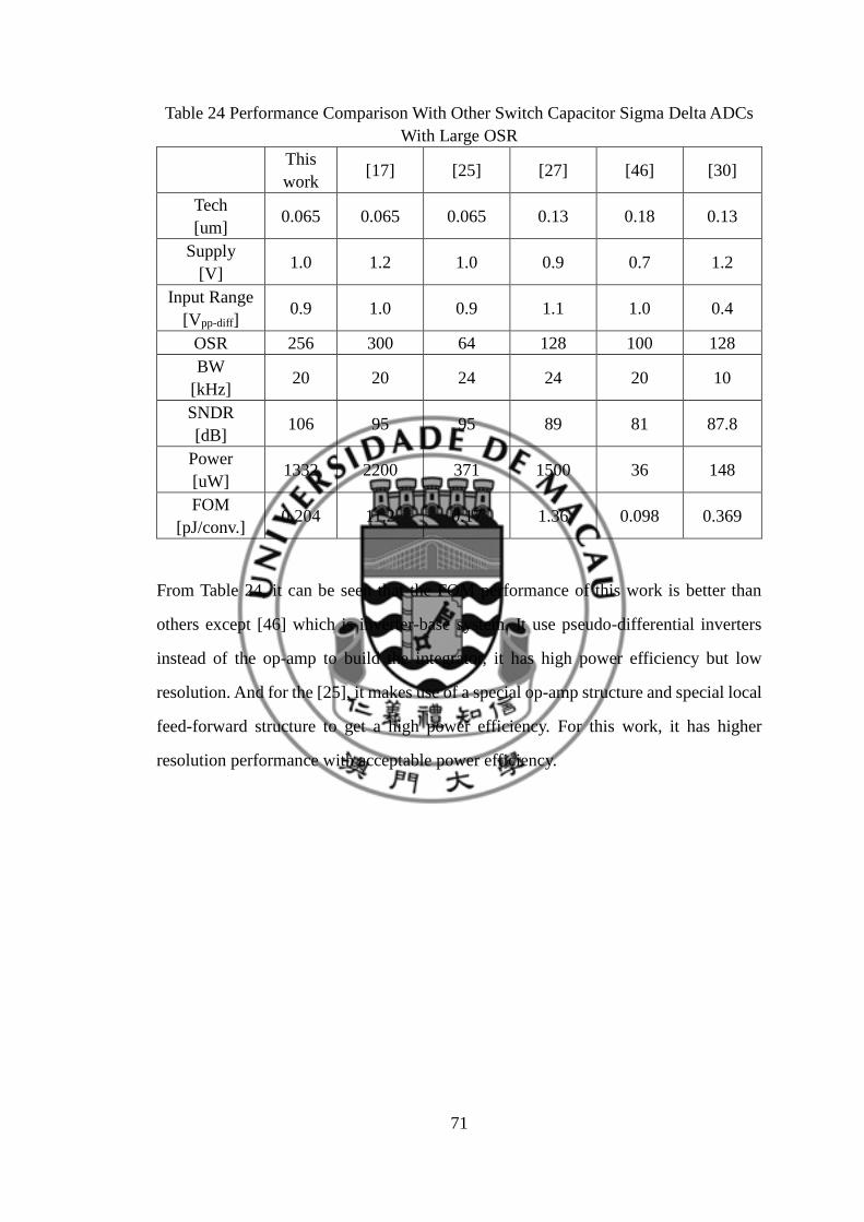
71
Table 24 Performance Comparison With Other Switch Capacitor Sigma Delta ADCs
With Large OSR
This
work [17] [25] [27] [46] [30]
Tech
[um] 0.065 0.065 0.065 0.13 0.18 0.13
Supply
[V] 1.0 1.2 1.0 0.9 0.7 1.2
Input Range
[Vpp-diff] 0.9 1.0 0.9 1.1 1.0 0.4
OSR 256 300 64 128 100 128
BW
[kHz] 20 20 24 24 20 10
SNDR
[dB] 106 95 95 89 81 87.8
Power
[uW] 1332 2200 371 1500 36 148
FOM
[pJ/conv.] 0.204 11.2 0.17 1.36 0.098 0.369
From Table 24, it can be seen that the FOM performance of this work is better than
others except [46] which is inverter-base system. It use pseudo-differential inverters
instead of the op-amp to build the integrator, it has high power efficiency but low
resolution. And for the [25], it makes use of a special op-amp structure and special local
feed-forward structure to get a high power efficiency. For this work, it has higher
resolution performance with acceptable power efficiency.

72
VIII CONCLUSION
In this project, for audio application, a 3rd order CRFB (Cascade of Resonators with
Distributed Feedback) sigma delta analog to digital converter with Charge-pump
integrator and 1.5 bit quantizer is designed to achieve the target (SNDR≥105dB) set
after product survey. Since the high resolution is required in a low bandwidth, a 3rd order
sigma-delta modulator with a high OSR (256) is chosen. 1.5 bit quantizer is chosen
because it has the advantages of multi-bit quantizer but doesn’t affect the linearity of
the DAC. After the comparison and simulation in Matlab, the CRFB architecture is
chosen for its high SNDR, acceptable integrator input swing and simple adder.
Moreover, based on the simulation in Matlab, the behavioral model of the system is
obtained, which determines the DC gain, GBW and the slew-rate requirement of the op-
amp of the integrators. After that, the circuit is designed in Cadence with 65nm CMOS
technology. To implement the integrator and passive adder, the switch capacitor
technique is used. And since the first integrator is power hungry, a special integrator
called Charge-pump integrator which costs the less power than the conventional one is
chosen. For the op-amp design, the different structure chosen because of the different
requirement. And for the 1.5 bit quantizer, it makes use of the switch capacitor to
compare the input of the quantizer with the reference voltage. Finally, NMOS switch,
PMOS switch, CMOS switch and bootstrap switch are used according to linearity of
each switch.
As a result (Table 25), with a full-scale input of 900mVpp differential the CRFB ADC
using charge-pump integrator achieves 106 dB SNDR and 107dB dynamic range in
audio bandwidth (20kHz), while consuming 1.332mW power.
Table 25 The Performance of System
Performance
Technology 65nmCMOS
Sampling Frequency 10.24MHz
Bandwidth 20kHz
Peak SNDR 106dB
Dynamic Range 107dB
Power consumption 1.332mW

73
FOM 204f/conv.
Future work
From this project, this sigma delta ADC provides a selection for audio applications. So,
its performance would be progressively significant in the further. Here it is given a brief
blueprint for the future work in the next level study.
Considering the further requirement of energy-saving, the supply voltage would be
decreased, so the low power low voltage performance would be the main research issue.
In detail, the operational transconductance amplifier (OTA) is the bottleneck for
reducing the power dissipation. Circuits could be used in schematic to remove the need
for OTAs, or even replacing the OTA with other structures like inverter. Take an
overview from system level, because of the stability consideration, some high-order
structures could be built in the circuit level in further project. Moreover, for improving
the performance, some extra ideas could be constructed like Op-amp sharing technique,
which performs noise shaping with only one Op-amp, also very suitable for low–voltage
environment; Double-sampling Switch, which samples both phases, thus doubles the
OSR with the same power consumption;
Last but not least, continuous time sigma delta ADC, which has become a hot research
area, bringing the implicit anti-aliasing filter. It offers unique features that greatly reduce
the challenges of deploying ADCs in high-performance systems with high power-
efficiency.
All in all, the studies carry on to fulfill the requirements of fast technical development.
Those architectures could be our future targets which could be combined with this
current work.

74
IX REFERENCE
[1] Aksin, Devrim, Mohammad A. Al-Shyoukh, and Franco Maloberti. "A
bootstrapped switch for precise sampling of inputs with signal range beyond supply
voltage." Custom Integrated Circuits Conference, 2005. Proceedings of the IEEE
2005.
[2] Audio ADCs,http://www.akm.com/akm/en/product/detail/0019/
[3] Aziz, Pervez M. "Multi-band oversampled noise shaping analog to digital
conversion." Engineering Documents (1996): 1.
[4] Aziz, Pervez M., and Henrik V. Sorensen. "An overview of sigma-delta converters."
Signal Processing Magazine, IEEE 13.1 (1996): 61-84.
[5] Bill Klein, Senior Applications Engineer, Texas Instruments “SIGNAL CHAIN
BASICS Series (Part 4): Introduction to analog/digital converter (ADC) types”
[6] Boser, Bernhard E., and Bruce A. Wooley. "The design of sigma-delta modulation
analog-to-digital converters." Solid-State Circuits, IEEE Journal of 23.6 (1988):
1298-1308.
[7] Bourdopoulos, G. I., Anastassopoulos, V., Pnevmatikakis, A., & Deliyannis, T. L.
(2003)."Delta-sigma modulators: modeling,design and applications."Imperial
College Press.
[8] Brandt, Brian P., Drew E. Wingard, and Bruce A. Wooley. "Second-order sigma-
delta modulation for digital-audio signal acquisition." Solid-State Circuits, IEEE
Journal of 26.4 (1991): 618-627.
[9] Brannon, Brad. "Sampled systems and the effects of clock phase noise and jitter."
Analog Devices App. Note AN-756 (2004).
[10] Bult, Klaas, and Govert JGM Geelen. "The CMOS gain-boosting technique."
Analog Integrated Circuits and Signal Processing 1.2 (1991): 119-135.
[11] C.-H. Kuo, D.-Y. Shi, and K.-S. Chang, “A low-voltage fourth-order cascade delta-
sigma modulator in 0.18- m CMOS,” IEEE Trans. Circuits Syst. I, Reg. Papers, vol.
57, no. 9, pp. 2450–2461, Sep. 2010.
[12] Chang, Teng-Hung, and Lan-Rong Dung. "Fourth-Order Cascaded Modulator

75
Using Tri-Level Quantization and Bandpass Noise Shaping for Broadband
Telecommunication Applications." Circuits and Systems I: Regular Papers, IEEE
Transactions on 55.6 (2008): 1722-1732.
[13] Chen, Zhijie, et al. "A 22.4 μW 80dB SNDR ΣΔ modulator with passive analog
adder and SAR quantizer for EMG application." Solid State Circuits Conference
(A-SSCC), 2012 IEEE Asian. IEEE, 2012.
[14] Choksi, Ojas, and L. Richard Carley. "Analysis of switched-capacitor common-
mode feedback circuit." Circuits and Systems II: Analog and digital signal
processing, IEEE Transactions on 50.12 (2003): 906-917.
[15] Christen, Thomas. "A 15-bit 140-Scalable-Bandwidth Inverter-Based Modulator
for a MEMS Microphone With Digital Output." IEEE JSCC(2013): 1-1.
[16] Daliri, M., Mohammad Maymandi-Nejad, and Khalil Mafinezhad. "Distortion
analysis of bootstrap switch using Volterra series." Circuits, Devices & Systems,
IET 3.6 (2009): 359-364.
[17] Dorrer, L., et al. "A 2.2 mW, continuous-time sigma-delta ADC for voice coding
with 95dB dynamic range in a 65nm CMOS process." Solid-State Circuits
Conference, 2006. ESSCIRC 2006. Proceedings of the 32nd European. IEEE, 2006.
[18] FONG TEK KEI, 2013. "A 103dB Dynamic Range, 106dB SNDR Sigma-Delta
ADC for Audio Application". Final Year Report, University of Macau, Macau.
[19] Goes, João, et al. "3.7 A 0.9 V∆ Σ Modulator with 80dB SNDR and 83dB DR Using
a Single-Phase Technique." (2006).
[20] International Bureau of Weights and Measures, Taylor, B. N., & Thompson, A.
(2001). The international system of units (SI).US Department of Commerce,
Technology Administration, National Institute of Standards and Technology.
[21] J. Candy and G. Temes: “Oversampling methods for A/D and D/A conversion” in
Oversampling Delta-Sigma Data Converters, pp. 1-25, IEEE Press,1992.
[22] J. Goes, B. Vaz, R. Monteiro, and N. Paulino, “A 0.9 V sigma-delta modulator with
80 dB SNDR and 83 dB DR using a single-phase technique,” in Proc. IEEE Int.
Solid-State Circuits Conf. (ISSCC) Dig. Tech. Papers,Feb. 2006, pp. 191–200.
76
[23] Jim LeClare, Principal Member of Technical Staff, Smart Grid Solutions Jun 27,
2003. “A Simple ADC Comparison Matrix”tutorial 2094 from maximintegrated.
[24] Kanemoto, Daisuke, Toru Ido, and Kenji Taniguchi. "A 7.5 mW 101dB SNR low-
power high-performance audio delta-sigma modulator utilizing opamp sharing
technique." SoC Design Conference (ISOCC), 2011 International. IEEE, 2011.
[25] Liu, L., et al. "A 95dB SNDR audio ΔΣ modulator in 65nm CMOS." Custom
Integrated Circuits Conference (CICC), 2011 IEEE. IEEE, 2011.
[26] M. Dessouky and A. Kaiser, “Very Low-Voltage Delta-Sigma Modulator with 88
dB Dynamic Range Using Local Switch Bootstrapping”. IEEE J.Solid-State
Circuits, Vol. 36, No. 3, pp. 349-355, Mar 2001
[27] M. G. Kim, G.-C. Ahn, P. Hanumolu, S.-H. Lee, S.-H. Kim, S.-B. You,J.-W. Kim,
G. C. Temes, and U.-K. Moon, “A 0.9 V 92 dB double-sampled switched-RC delta-
sigma audio ADC,” IEEE J. Solid-State Circuits, vol. 43, no. 5, pp. 1195–1206,
May 2008.
[28] Malcovati, Piero, et al. "Behavioral modeling of switched-capacitor sigma-delta
modulators." Circuits and Systems I: Fundamental Theory and Applications, IEEE
Transactions on 50.3 (2003): 352-364.
[29] Maloberti, Franco. "Data converters". Vol. 1. Berlin: Springer, 2007.
[30] Nilchi, A., and D. A. Johns. "Charge-pump based switched-capacitor integrator for
ΔΣ modulators." Electronics letters 46.6 (2010): 400-401.
[31] Oppennheim and R. Schafer,"Discrete Time Signal Processing", (Pren-tice-Hall,
1989).
[32] Perez, Aldo Pena, Victor R. Gonzalez-Diaz, and Franco Maloberti. "ΣΔ Modulator
with op-amp gain compensation for nanometer CMOS technologies." Circuits and
Systems (LASCAS), 2012 IEEE Third Latin American Symposium on. IEEE, 2012.
[33] Quantities, A. V., & Motion, C. P. PHYSICAL SCIENCE PHYS 101 Credit Hours
General Education Core 7 Natural Science Catalog Description.
[34] Ranjbar, Mohammad, G. Roientan Lahiji, and Omid Oliaei. "A low power third
order delta-sigma modulator for digital audio applications." Circuits and Systems,

77
2006. ISCAS 2006. Proceedings. 2006 IEEE International Symposium on. IEEE,
2006.
[35] Razavi, Behzad. Design of analog CMOS integrated circuits. Tata McGraw-Hill
Education, 2002.4
[36] Schreier, Richard, and Gabor C. Temes. Understanding delta-sigma data converters.
Vol. 74. Piscataway, NJ: IEEE press, 2005.
[37] Steensgaard, Jesper. "Bootstrapped low-voltage analog switches."Circuits and
Systems, 1999. ISCAS'99. Proceedings of the 1999 IEEE International Symposium
on. Vol. 2. IEEE, 1999.
[38] Steven R. Norsworthy, Richard Schreier, Gabor C. Temes, “Delta-Sigma Data
Converters - Theory, Design, and simulation”,Motorola and Oregon State
University, 1997 by the IEEE 345 East 47th street, New York, NY 10019-2394.
[39] Tao, Hai, Laszlo Toth, and John M. Khoury. "Analysis of timing jitter in bandpass
sigma-delta modulators." Circuits and Systems II: Analog and Digital Signal
Processing, IEEE Transactions on 46.8 (1999): 991-1001.
[40] TI ADC PRODUCTS http://www.ti.com/lsds/ti/audio-ic/audio-adc-product.page
[41] TI company audio application
page,http://www.ti.com/lsds/ti/analog/audio/applications_tab.page
[42] Vijay, U. K., and Amrutur Bharadwaj. "Continuous time sigma delta modulator
employing a novel comparator architecture." VLSI Design, 2007. Held jointly with
6th International Conference on Embedded Systems., 20th International
Conference on. IEEE, 2007.
[43] Watkinson, J. (2013). Art of digital audio. CRC Press. IEC 60908 (published in
1987).
[44] Wei, H., Chan, C. H., Chio, U. F., Sin, S. W., Seng-Pan, U., Martins, R. P., &
Maloberti, F. (2012). "An 8-b 400-MS/s 2-b-per-cycle SAR ADC with resistive
DAC. "Solid-State Circuits, IEEE Journal of, 47(11), 2763-2772.
[45] Xiaofeng, Wu, et al. "A bootstrapped switch employing a new clock feed-through
compensation technique." Journal of Semiconductors 30.12 (2009): 125007.

78
[46] Y. Chae and G. Han, “Low voltage, low power, inverter-based switched-capacitor
delta-sigma modulator,” IEEE J. Solid-State Circuits, vol. 44, no. 2, pp. 458–472,
Feb. 2009.
[47] Zanbaghi, Ramin, et al. "A 75dB SNDR, 10MHz conversion bandwidth stage-
shared 2-2 MASH ΔΣ modulator dissipating 9mW." Custom Integrated Circuits
Conference (CICC), 2011 IEEE. IEEE, 2011.