Embed Size (px)
Citation preview

A 0.05-mm2 110-µW 10-b Self-Calibrating Successive Approximation
ADC Core in 0.18-µm CMOS
Yasuhide Kuramochi1,2, Akira Matsuzawa2,and Masayuki Kawabata1
1 Advantest Laboratories Ltd., Miyagi, Japan 2 Tokyo Institute of Technology , Tokyo, Japan
2
Outline
• Background
• ADC core architecture
• Calibration system
• Measurement results
• Conclusions
3
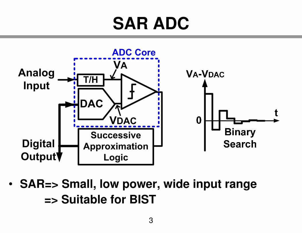
SAR ADC
• SAR=> Small, low power, wide input range
=> Suitable for BIST
Analog
Input
Digital
Output
Successive
Approximation
Logic
DAC
T/H
VA
VDAC
ADC Core
4
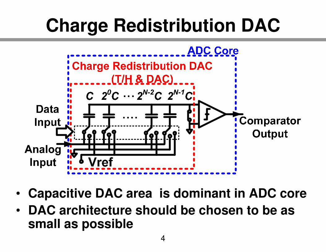
Charge Redistribution DAC
• Capacitive DAC area is dominant in ADC core
• DAC architecture should be chosen to be as small as possible

5
Outline
• Background
• ADC core architecture
• Calibration system
• Measurement results
• Conclusions

6
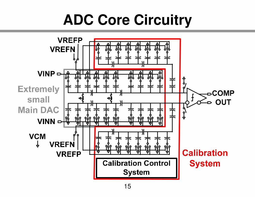
Proposed ADC Core Circuitry
COMP
OUT
Extremely
small
Main DAC
VCM
VINN
VREFP
VREFNCalibration
System
VINP
VREFN
VREFP
Calibration Control
System

7
ADC Core Circuitry
COMP
OUT
Extremely
small
Main DAC
VCM
VINN
VREFP
VREFNCalibration
System
VINP
VREFN
VREFP
Calibration Control
System

8
Realizing Small DAC
• Decreasing the area of DAC=> Small unit capacitor: C=20fF
No dummy capacitor around DAC=> Calibration is inevitable for small DAC
Dummy
cap.
DAC
cap.
Conventional
DACProposed
DAC
Cal
DAC
Main
DAC

9
Upper Bit DAC Architecture
• SNR is limited by total capacitance at DAC Outnode
• To increase total capacitance, the upper bit DAC is composed of binary capacitor DAC
10
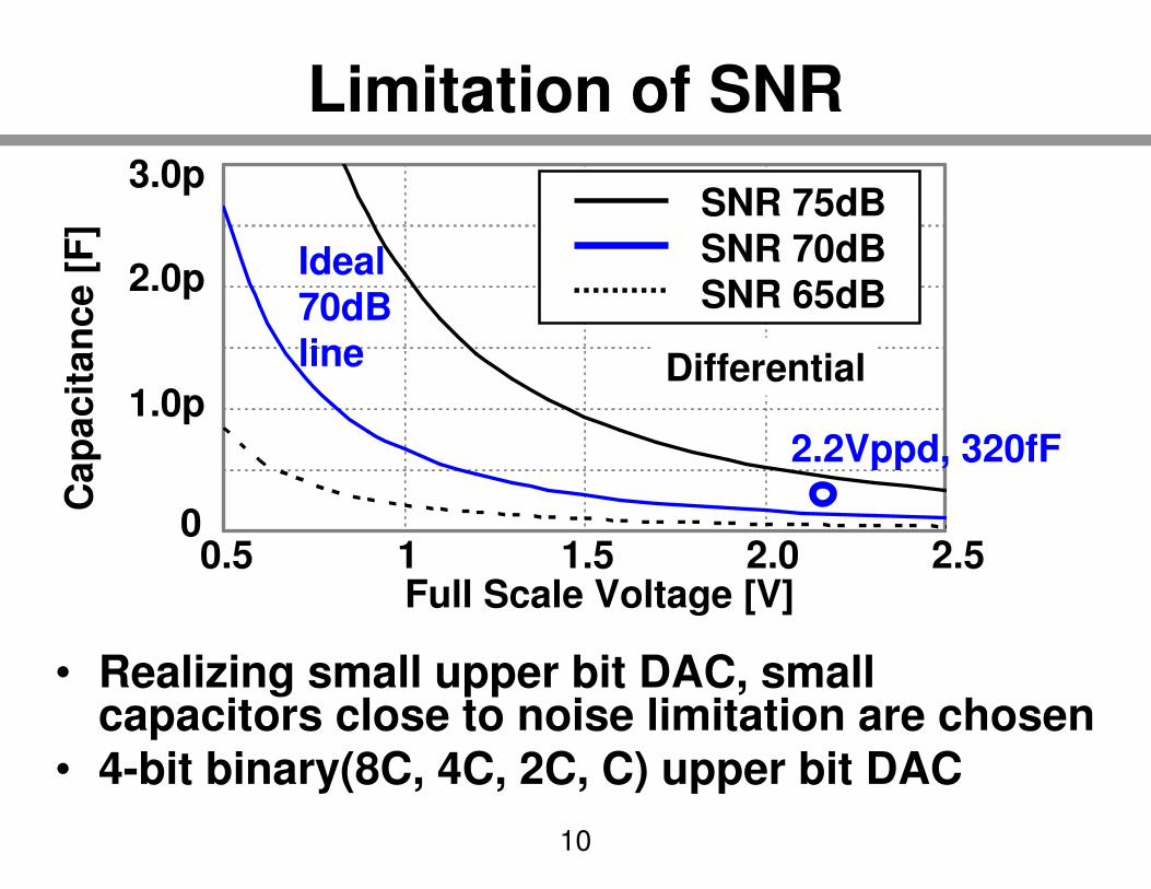
Limitation of SNR
• Realizing small upper bit DAC, small capacitors close to noise limitation are chosen
• 4-bit binary(8C, 4C, 2C, C) upper bit DAC
3.0p
2.0p
1.0p
0
Cap
acit
an
ce [
F]
Full Scale Voltage [V]0.5 1 1.5 2.52.0
SNR 75dBSNR 70dBSNR 65dB
Differential
2.2Vppd, 320fF
Ideal70dBline
11
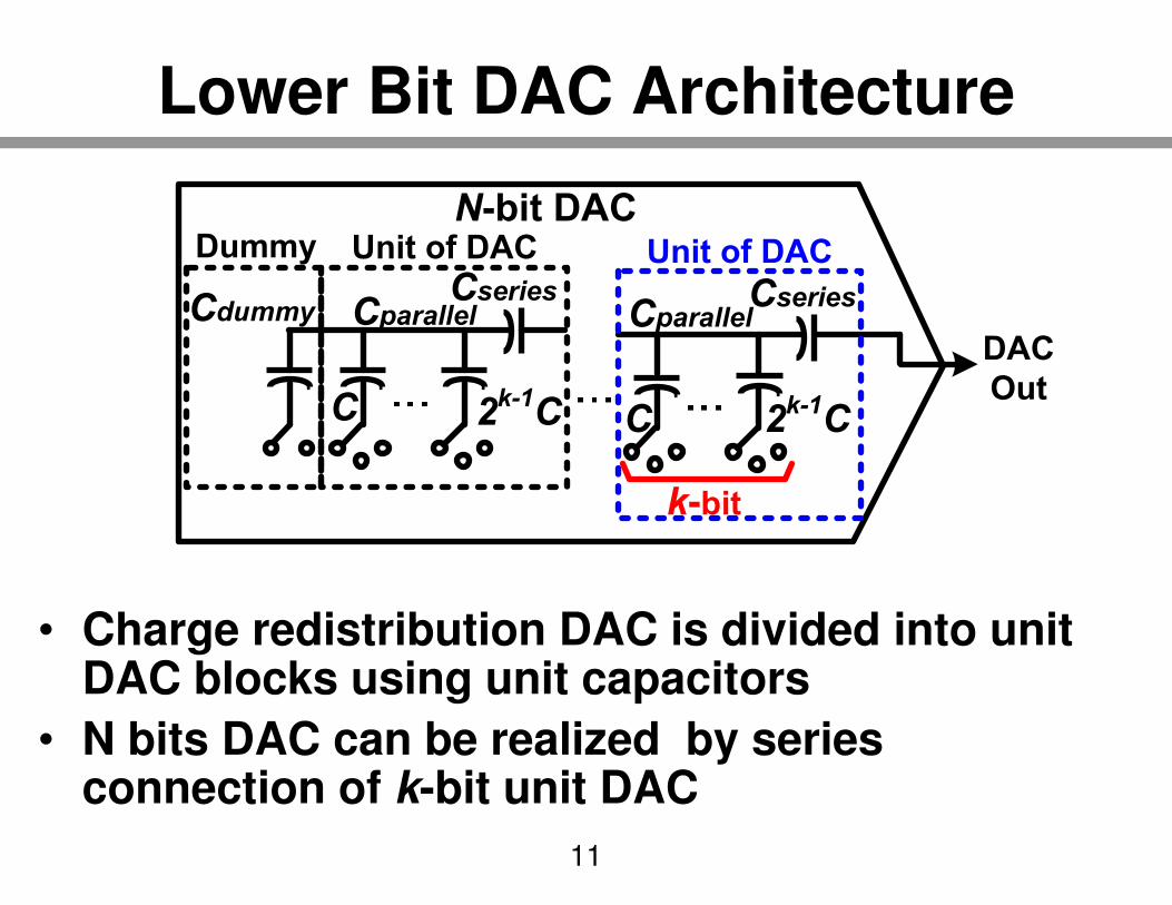
Lower Bit DAC Architecture
• Charge redistribution DAC is divided into unit DAC blocks using unit capacitors
• N bits DAC can be realized by series connection of k-bit unit DAC
DAC
Out
Cparallel
N-bit DACDummy Unit of DAC
CparallelCseries
Unit of DAC
Cdummy
C 2k-1C2
k-1CC
Cseries
k-bit

12
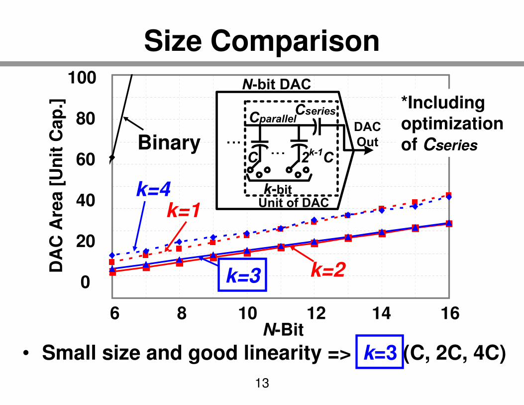
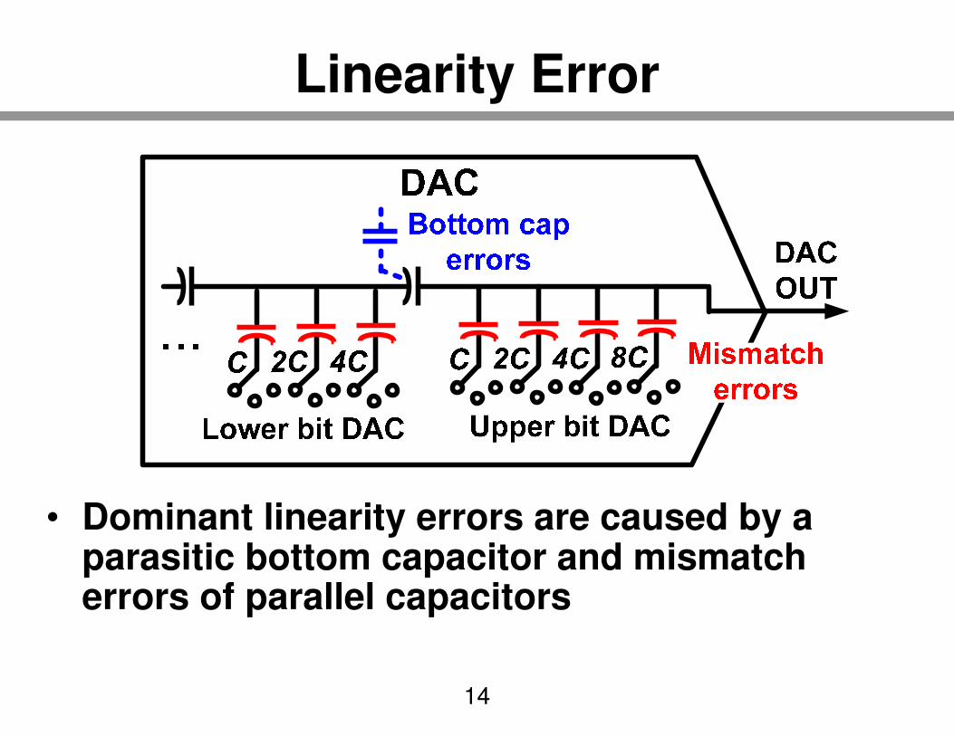
Linearity Error of Unit DAC
• Dominant linearity error is caused by parasitic bottom capacitor
=> Large “k” is better for linearity
13
Size Comparison
• Small size and good linearity => k=3 (C, 2C, 4C)
100
80
60
40
20
0
DA
C A
rea [
Un
it C
ap
.]
N-Bit6 8 10 12 14 16
k=3 k=2
Binary
k=1k=4
*Includingoptimizationof Cseries
Cparallel
Unit of DAC
C 2k-1C
Cseries
k-bit
DAC
Out
N-bit DAC
14
Linearity Error
• Dominant linearity errors are caused by a parasitic bottom capacitor and mismatch errors of parallel capacitors
15
ADC Core Circuitry

16
Calibration System
DIGITAL
OUT
ANALOG
IN
MAIN
DAC
T/H
CAL DAC
MAIN
SAR
LOGIC
MEAS.
CONT.
CAL
MEM.
CAL
SAR
LOGIC
Calibration System
• CAL range: from -16LSB to 16LSB
with 1/4LSB step

17
Self-measurement System
• The CAL DAC and comparator operates as error measurement ADC with a SAR algorithm
MAIN
DAC
Cap error
CAL
SAR
ADC
CAL
MEM.
18
Measurement of Offset
• Measurement sequence :1. Measurement of the offset2. Measurement of the upper 5-bit
• CAL SAR search for Voffset

19
Measurements of Cap. Errors
• Measurement sequence :
1. Measurement of the offset
2. Measurement of the upper 5-bit
• CAL SAR search for ΔΔΔΔCk_err – CCAL=0
Voffset
VCM
CCAL
Ck Ck_err
C(k+1~N)
VREFP
VREFN
Ck-1C1Cdum
SAR
Cm+Cdum=Ckk-1
m=1

20
Conversion Sequence
• Conversion Sequence :
Main DAC output is calibrated with CAL DAC based on measurement data
21
Outline
• Background
• ADC core architecture
• Calibration system
• Measurement results
• Conclusions

22
Chip Micrograph
• 0.18µm CMOS, 1-poly, 6-metal Layers, MIM Capacitor
• Control logics are composed of an off chip FPGA
Main DAC Cal DAC
Comparator
550µm
95µm

23
Measured Spectrum
• Fsample 1MS/s, Fin 1kHz, 1.8V Supply
Frequency [kHz]0 1 2 3 4 5
Calibration Off
Calibration On
SFDR=48.2dB
SFDR=72.3dB40
80
0
[dB
]
40
80
0
[dB
]
25.1dB

24
Dynamic Performance
• Fsample 1MS/s, 1.8V Supply
Input frequency [Hz]1k 10k 100k 1M
SN
DR
[d
B]
SF
DR
[d
B]
40
60
80
40
60
Calibration Off
Calibration On
Calibration Off
Calibration On
23.3dB
9.0dB

25
ADC Performance Summary 1
1.8VPower Supply
110µW(Analog)Power Consumption
2.2VppdFull Scale Voltage
69.8dBSFDR@nyquist
51.1dBSNDR@nyquist
1MSps (12MHz clock)Sampling Rate
95µm x 550µm=0.05mm2Active Area
10bitResolution
0.18µm, 1poly, 6metal CMOSTechnology

26
ADC Performance Summary 2
[1] J. Craninckx, et. al., “A 65fJ/Conversion-Step, 0-to-50MS/s 0-to-0.7mW 9bit Charge-Sharing SAR ADC in 90nm Digital CMOS”, ISSCC 2007
[2] Y. Jeon, et. al., “A 4.7mW 0.32mm2 10b 30MS/s Pipelined ADC Without a Front-End S/H in 90nm CMOS”, ISSCC 2007
12Bit11Bit10Bit9BitF
oM
[J/c
on
v. ste
p]
100f
0.01 0.1 1 10
1p
10p
10f
Area [mm2]
This work (0.18µm)
Good
This work(Estimationwith Digital)
[1] (90nm)
[2] (90nm)[2] (90nm)
*MSps ADC
27
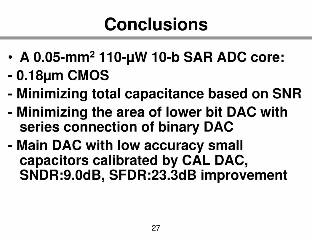
Conclusions
• A 0.05-mm2 110-µW 10-b SAR ADC core:
- 0.18µm CMOS
- Minimizing total capacitance based on SNR
- Minimizing the area of lower bit DAC with series connection of binary DAC
- Main DAC with low accuracy small capacitors calibrated by CAL DAC, SNDR:9.0dB, SFDR:23.3dB improvement