Embed Size (px)
Citation preview

92 IEEE TRANSACTIONS ON MICROWAVE THEORY AND TECHNIQUES, VOL. 62, NO. 1, JANUARY 2014
Transformer-Based Broadband High-Linearity HBT-Boosted Transconductance MixersJian Zhang, Mingquan Bao, Dan Kuylenstierna, Member, IEEE,Szhau Lai, Student Member, IEEE, and Herbert Zirath, Fellow, IEEE
Abstract—A -boosted transconductance configurationmixer is proposed. Based on this topology, two broadband mono-lithic InGaP HBT mixers, one single device and one balanced,have been developed for – -band applications. The singledevice mixer has a conversion gain of 4.5 1.5 dB within theRF frequency range from 5 to 17 GHz. The balanced design hasabout 3.5 1.5-dB conversion gain within a frequency rangeof 6–18 GHz. The two mixers have very good linearity with athird-order intermodulation intercept point (IIP3) higher than 16and 20 dBm for the single device mixer and single balanced mixer,respectively. Both mixers are pumped by a local oscillator powerof 5 dBm. To the authors’ best knowledge, the designed mixersdemonstrate the highest IIP3 with positive conversion gain in thisfrequency range. Compact designs are achieved with chip sizesless than 0.5 mm . DC power consumptions are 30 and 50 mW,for the single device and single balanced mixer, respectively.
Index Terms— -boosted, InGaP HBT, transconductancemixer, transformer balun.
I. INTRODUCTION
H IGH-LINEARITY transceivers are mandatory in mi-crowave and millimeter-wave high data-rate commu-
nication systems when using high-order modulation schemes.The mixer in such systems is responsible for the frequency con-version, and often limits the linearity of the transceiver. In thereceiver, the down-conversion mixer is required to be able tohandle large input signals from the low-noise amplifier (LNA)without causing significant intermodulation (IM), harmonicgeneration, and gain compression[1], [2], .The frequency conversion in mixers is generally achieved
through two distinctly different mechanisms; by switching the
Manuscript received August 08, 2013; revised October 29, 2013; acceptedOctober 30, 2013. Date of publication November 28, 2013; date of current ver-sion January 06, 2014. The work of J. Zhang was supported by the NationalSpace Research Program (NRFP) project “Advanced MMIC Functions” car-ried out by RUAG Space AB and Chalmers University.J. Zhang was with the Department of Microtechnology and Nanoscience
(MC2), Chalmers University of Technology, SE-412 96 Göteborg, Sweden.He is now with the Shanghai Institute of Microsystem and InformationTechnology, Chinese Academy of Sciences, Shanghai 200050, China (e-mail:[email protected]).M. Bao is with the Microwave and High Speed Electronics Research Center
(MHSERC), Ericsson AB, SE-431 84, Mölndal, Sweden.D. Kuylenstierna and S. Lai are with the GigaHertz Centre, Department of
Microtechnology and Nanoscience (MC2), Chalmers University of Technology,SE-412 96 Göteborg, SwedenH. Zirath is with the GigaHertz Centre, Department of Microtechnology and
Nanoscience (MC2), Chalmers University of Technology, SE-412 96 Göteborg,Sweden, and also with the Microwave and High Speed Electronics ResearchCenter (MHSERC), Ericsson AB, SE-431 84, Mölndal, Sweden.Color versions of one or more of the figures in this paper are available online
at http://ieeexplore.ieee.org.Digital Object Identifier 10.1109/TMTT.2013.2291712
RF current with the LO frequency, secondly utilizing the tran-sistor’s nonlinear (quasi-square law) characteristic to generatethe desired frequency signal. The former is normally realizedwith the so-called Gilbert cell [3]. This type of mixer couldprovide a decent conversion gain, port isolation, and noisefigure; however, its linearity is modest, limited by the linearityof the differential transconductance pair at the RF input stage.To achieve simultaneously a high linearity and a good con-version gain, many linearization methods have been applied,such as adding source degeneration resistors [4], using a foldedcascode Gilbert cell [5], [6] and a bisymmetric class-AB inputstage [7]–[9], employing out-of-band harmonic terminations[10], and integrating a diode linearizer [11]. However, theselinearization techniques, in general, are at costs of either circuitcomplexity or conversion gain.Alternatively, transconductance mixers ( -mixer) have
demonstrated better linearity performance than their Gilbertcounterpart. They have been implemented in CMOS [12] andSiGe BiCMOS [13], [14] technologies. The -mixer consistsof either a single-transistor or parallel-connected transistors. Inorder to produce the time-varying transconductance and realizethe frequency conversion, the local oscillator (LO) voltage isnormally applied at the base (or gate) terminal. It requires acombiner to provide a linear summation of the LO and RFsignal. If using lumped components ( , ) to build such apower combiner, its frequency bandwidth is quite narrow(less than 15% [13]). If using a broadband Wilkinson powercombiner, it is normally too large to be integrated on-chip fora frequency lower than 20 GHz. Alternatively, the LO and RFsignals could be added at the transistor’s emitter (source) andbase (gate) separately to realize a emitter (source) pumpedconfiguration [15]–[17] in order to avoid the power combiner.However, these types of emitter pumped mixers suffer from aconversion loss of 3 7 dB and requires a large LO power,e.g., 7 10 dBm to achieve good performances. Furthermore,the LO and RF signals could be added at the drain and gateseparately, to form a so-called drain mixer [18], [19]. Such amixer, however, generally achieved a higher conversion lossand poorer linearity than either an LO source or gate pumpedmixer.In order to improve conversion gain, linearity, and to reduce
LO power consumption, the emitter-pumped transconductancemixer is modified by using a -boosted technique. This tech-nique, i.e., introducing an inverting amplification between thebase and emitter terminals has been used in differential LNAsand voltage-controlled oscillators (VCOs), as well as multiplierdesigns [20]–[22], shown in Fig. 1. Here, it is used for mixerdesigns to improve the merit of interest. In order to prove this
0018-9480 © 2013 EU
ZHANG et al.: TRANSFORMER-BASED BROADBAND HIGH-LINEARITY HBT -BOOSTED TRANSCONDUCTANCE MIXERS 93
Fig. 1. Basic schematic of -boosted feedback.
Fig. 2. (a) Conventional transconductance mixer. (b) Transformer-coupled-boosted transconductance mixer.
concept, the proposed mixer topology has been implementedwith InGaP HBT technology.This paper is organized as follows. Section II details the prin-
ciple of the transformer coupling -boost scheme applied to atransconductance mixer. Implementations of mixer circuits arediscussed in Section III. The experimental results are presentedin Section IV. Finally, conclusions are given in Section V.
II. TRANSFORMER COUPLED -BOOSTED THEORY
As shown in Fig. 2, a transformer is used in a “ -boosted”configuration, which acts as an inverting amplifier with gain lessthan 0 dB, and avoids nonlinearity resulting from an active am-plifier. The transformer consists of primary and secondarywind-ings, and , respectively. Magnetic coupling betweenand provides an antiphase relationship between the emitterand base terminal. The RF signal is applied at the base, and itsinverted one is added at the emitter, thus the RF signal swingacross the base–emitter junction is boosted.To study the impact of transformer coupled -boosted
topology on bandwidth and effective transconductance, aconventional inductor degenerated configuration without andwith transformer coupling were considered, as shown inFig. 2(a) and (b). In the small-signal expression, are theparallel combinations of the base-charging capacitance andbase–emitter junction capacitance and an extra capacitance.Starting with the circuit in Fig. 2(a), it is straightforward to
prove that the input impedance is described by
(1)
Accordingly, the circuit appears to be a series- net-work with , resonant frequency
, and quality factor , where
(2)
Next, consider the transformer-coupled -boosted config-uration in Fig. 2(b), where and are identical to its con-ventional counterpart.The input admittance of the transformer-coupled-boosted configuration is found on Fig. 2(b). Applying
Kirchhoff’s current law (KCL) at the base and emitter terminalswith mutual inductance between the primary and secondarywindings yields [21], [23]
(3)
(4)
(5)
(6)
Solving (3)–(6) with coupling coefficientand turn-ratio gives the input admittance
(7)
where
(8)
(9)
(10)
Thus, similar to (1), the input admittance of the transformercoupled -boosted configuration appears as a parallelcircuit resonant at withinput admittance , andquality factor , where
(11)
94 IEEE TRANSACTIONS ON MICROWAVE THEORY AND TECHNIQUES, VOL. 62, NO. 1, JANUARY 2014
Since both circuits in Fig. 2 are designed to resonate at the samefrequency and as mentioned earlier, includes a shunt capac-itance , which can be appropriately selected to ensuresatisfies the resonance condition mathematically described in(12) as follows [23]:
(12)
Since the quality factor of the matching network is inverselyproportional to the bandwidth, from (12), one observes that thenew condition gives
(13)
where is effective matching bandwidth.Therefore, as compared to the conventional inductor degener-
ated configuration, transformer coupled -boosted topologyeffectively achieves a higher matching bandwidth.The equivalent transconductance of the transformer-cou-
pled -boosted configuration can also be found via solving(3)–(6),
(14)compared to the conventional inductor degenerated configura-tion, shown in Fig. 2(a), which has the effective transconduc-tance , where
(15)
As a result, (13) and (14) give
(16)
Further insight regarding the relationship betweenand can be obtained by specifying
GHz and
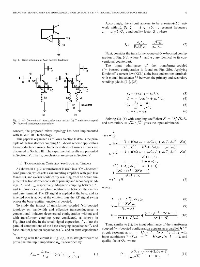
Fig. 3. Effective transconductance increased as the function of .
( is normally around 1 nH and is constrained to be lessthan 100 ms), as shown in Fig. 3.Fig. 3 offers intuition on the impact of on the
transconductance boosted effect. As the increases of and ,the effective transconductance can be improved by a factor ofup to 3.Note that the improvement of the effective transconductance
also relates with the turns ratio and coupling factor . How-ever, due to the nonideality of an on-chip transformer, i.e., par-asitic resistance and capacitance, which results in losses andself-resonance, a turn ratio of 2 is chosen. While, the couplingfactor could be up to 0.8 employing multi-layer broadsidecoupling [24].
III. MIXERS DESIGN
To verify the principle of the -boosted transconduc-tance mixer, two mixers, a single device mixer and a singlebalanced mixer, have been designed. Both mixers are im-plemented in WIN Semiconductors 6-in InGaP–GaAs HBTprocess H01U-10. The emitter finger width is 1 m and
GHz. The prototype circuits utilize atwo-finger HBT with finger length 20 m and width 1 mto achieve simultaneous good conversion gain and linearityat the designed frequency range. The designs are based onan in-house developed compact large-signal HBT model,which is an extension of Chalmers-Mitsubishi HBT model[25]. The parameters are extracted using dc measurements,bias-dependent small-signal -parameters, and low-frequencynoise measurements. Most parameters can be extracted directlyfrom measurements, e.g., the maximum current gain BETA,respective to peak collect current and peak base voltage
. The ideality factors and are extracted fromGummel plots. The depletion and diffusion capacitances, aswell as the parasitic inductances and resistances, are extractedfrom the bias-dependent -parameters.
A. Single Device Mixer
The schematic of the proposed single device mixer is shownin Fig. 2(a). The circuit is configured as an emitter-pumped con-figuration, with an RF signal applied to the base terminal, andLO signal applied to the emitter terminal. Moreover, a resultantdown-conversion IF signal extracted from the collector terminal

ZHANG et al.: TRANSFORMER-BASED BROADBAND HIGH-LINEARITY HBT -BOOSTED TRANSCONDUCTANCE MIXERS 95
Fig. 4. (a) Layer stack. (b) Physical layout of the transformer.
and high frequency components are filtered out by a shunt ca-pacitor at the output port. provides a dc bias for the transistorand an ac ground for .Fig. 4(a) shows the adjacent metal layer stack of the process.
The top thicker metal layer, metal 2, has a thickness 2 m anda space 0.4 m to the lower thinner metal layer, metal 1, whichhas a thickness 1 m. At the bottom of the metal layer stack,there is a thin metal layer, , with thickness 0.3 m.Fig. 4(b) shows the proposed transformer with turn-ratio. The primary winding was fabricated with the top thick metal,metal 2, and the secondary one was fabricated with both metal 2and metal 1 to achieve a high coupling coefficient and compactsize. The metal width was chosen to be 20 m, as a tradeoff be-tween themetal loss and the parasitic capacitances. The first turnof the secondary winding was fabricated with metal 1, verticallystacked to the primary winding to realize broadside coupling,and the second turn was fabricated with metal 2, with ametal-to-metal spacing of 5 m, neighbor to the primary winding as closeas possible to realize a tight edge coupling. The geometry sizeof the designed transformer is 190 m 130 m and the simu-lated coupling coefficient is around 0.8. For the detailed de-sign equation about the transformer, we refer to [24].
B. Balanced Mixer
The proposed transformer coupled -boosted topology canalso be applied into the design of a balanced mixer to improvethe linearity and port isolation further.The schematic of the conventional and proposed balanced
mixer are shown in Fig. 5(a) and (b). Similar to the RF part, inorder to get a differential RF input signal, a transformer balunwas designed. It was implemented by grounding the center tapof the second winding. As shown in Fig. 5(c) and (d), is beconnected with the RF input; while differential outputis connected with the base terminals of the transistor pair. Asfor the LO part, in order to introduce an inverting amplifica-tion between the base and emitter terminals, shown in Fig. 5(b),a differential trifilar transformer with a turn ratio of 1:1:2 wasdesigned, as shown in Fig. 5(e) and (f). The transformer con-sists of three groups of windings of interwound 20- m-widemicrostrip lines with 5- m line spacing. The primary windingwas fabricated on the top thick metal, metal 2, and the secondarywinding was fabricated on metal 1. The power trans-mission from the primary input to secondary outputis realized via broadside coupling with a turn-ratio 1:1. Thesecond winding uses two turns; the first turn is fab-ricated on metal 2, and the second turn is fabricated on metal
1; the power transmission from the primary input to sec-ondary output is realized via both edge and broad-side coupling with a turn-ratio of 1:2. Finally, the central tapsof the secondary windings and the end terminal of the primarywinding are grounded together. Noted here, a cross-connec-tion is used to realize the antiphase magnetic coupling, as high-lighted in Fig. 5(b). The whole transformer has a compact sizeof 320 m 280 m.
IV. MEASUREMENTS RESULTS
The single device and balanced mixers are fabricated andmeasured. Fig. 6 shows chip photographs of the circuits. Thechip sizes of the single device and balanced mixer are 0.50 and0.62 mm including all the pads, respectively. The mixers weremeasured using on-wafer probing system with LO power of5 dBm and quiescent dc-bias current of 13 and 22 mA, respec-tively, from a 2.3-V voltage supplier. They were characterizedover the frequency range from 3 to 20 GHz.The conversion gain of the proposed mixers were measured
for a fixed IF frequency of 500 MHz with both RF and LOfrequencies swept in frequency up to 20 GHz. The RF signalpower was set to be 15 dBm. The conversion gains versus RFfrequency for both mixers are plotted in Fig. 7. The single de-vice mixer achieved a conversion gain of better than 3 dB overa wideband frequency from 6 to 15 GHz. A 3-dB bandwidthfor RF signal is 12 GHz, i.e., from 5 to 17 GHz with an av-erage conversion gain of 4.5 dB. The conversion gain peaks at8 and 14 GHz with 5.8 dB. On the other hand, the balancedmixer presented a 3-dB bandwidth across the RF frequency of6–18 GHz with a conversion gain variation of 3.5 1.5 dB. Thismixer’s gain is around 1.5–2 dB lower than its single devicecounterpart. The reason can be attributed to the loss of trans-former balun at RF input port. The measured conversion gainis consistently 1–2 dB lower than simulation for both mixers.Part of the difference seen between measurements and simula-tions can be attributed to frequency-dependent losses in the RFpath not accounted for by the RF power calibration procedure.Also, the input/output (I/O) ground–signal–ground (GSG) padsand coplanar waveguide (CPW) interconnects at the RF and LOinputs were not included in the simulations.Fig. 8 describes the conversion gain variations as the LO
power is swept from 4 to 8 dBm at a frequency of 12 GHz.We can find that approximate 5-dBm LO power is required torealize peak conversion gains for both mixers. Approximately2 dB more LO power was required to realize peak conversiongain for both mixers in measurement compared to simulation.This is due, in part, to the shifting of the LO (large-signal) inputimpedance level and inductors and capacitors component valuesdue to process variations also contribute to the observed discrep-ancies.Conversion gain versus IF frequency is plotted in Fig. 9 with
LO frequency equal to 14 GHz and LO power equal to 5 dBm.The 3-dB IF-bandwidth is determined by the on-chip IF filter,which yields a cutoff frequency around 0.8 GHz for single de-vice mixer and 1.9 GHz for the single balanced one.Since the magnetic coupling between the RF and LO signal
was introduced by the transformer, the LO-RF port isolationcharacteristic was very critical. The simulated and measured
96 IEEE TRANSACTIONS ON MICROWAVE THEORY AND TECHNIQUES, VOL. 62, NO. 1, JANUARY 2014
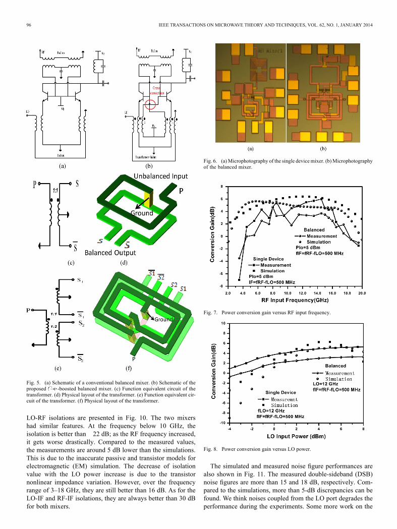
Fig. 5. (a) Schematic of a conventional balanced mixer. (b) Schematic of theproposed -boosted balanced mixer. (c) Function equivalent circuit of thetransformer. (d) Physical layout of the transformer. (e) Function equivalent cir-cuit of the transformer. (f) Physical layout of the transformer.
LO-RF isolations are presented in Fig. 10. The two mixershad similar features. At the frequency below 10 GHz, theisolation is better than 22 dB; as the RF frequency increased,it gets worse drastically. Compared to the measured values,the measurements are around 5 dB lower than the simulations.This is due to the inaccurate passive and transistor models forelectromagnetic (EM) simulation. The decrease of isolationvalue with the LO power increase is due to the transistornonlinear impedance variation. However, over the frequencyrange of 3–18 GHz, they are still better than 16 dB. As for theLO-IF and RF-IF isolations, they are always better than 30 dBfor both mixers.
Fig. 6. (a)Microphotography of the single devicemixer. (b)Microphotographyof the balanced mixer.
Fig. 7. Power conversion gain versus RF input frequency.
Fig. 8. Power conversion gain versus LO power.
The simulated and measured noise figure performances arealso shown in Fig. 11. The measured double-sideband (DSB)noise figures are more than 15 and 18 dB, respectively. Com-pared to the simulations, more than 5-dB discrepancies can befound. We think noises coupled from the LO port degrades theperformance during the experiments. Some more work on the

ZHANG et al.: TRANSFORMER-BASED BROADBAND HIGH-LINEARITY HBT -BOOSTED TRANSCONDUCTANCE MIXERS 97
Fig. 9. Power conversion gain versus IF frequency.
Fig. 10. LO-RF isolation versus RF input frequency.
Fig. 11. Noise figure versus RF frequency.
measurements and simulation would probably improve and tes-tify the results further.The linearity performance of a mixer, as evaluated in terms of
the third-order intermodulation intercept point (IIP3), is definedas the extrapolated point at which the amplitude of the third-order intermodulation (IM3) product and the IF fundamentalsignal are equal. Figs. 12 and 13 depict the IM3 product and
Fig. 12. IM3 and fundamental power for single device mixer.
Fig. 13. IM3 and fundamental power for balanced mixer.
Fig. 14. IIP3 and IM3 versus LO power.
fundamental signal power as functions of the RF input powerfor single device and balanced mixers, respectively. There aretwo signals fed to the RF input ports for IIP3 measurements,one at 8.5 GHz and the other at 8.51 GHz. The LO signal hasa frequency of eight single device mixer exhibiting an IIP3 of16 dBm and GHz and power level of 5 dBm. Fig. 12 shows
98 IEEE TRANSACTIONS ON MICROWAVE THEORY AND TECHNIQUES, VOL. 62, NO. 1, JANUARY 2014
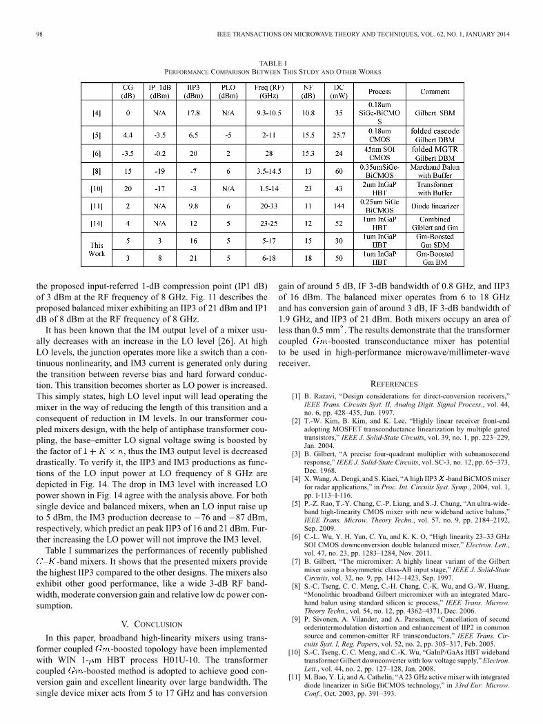
TABLE IPERFORMANCE COMPARISON BETWEEN THIS STUDY AND OTHER WORKS
the proposed input-referred 1-dB compression point (IP1 dB)of 3 dBm at the RF frequency of 8 GHz. Fig. 11 describes theproposed balanced mixer exhibiting an IIP3 of 21 dBm and IP1dB of 8 dBm at the RF frequency of 8 GHz.It has been known that the IM output level of a mixer usu-
ally decreases with an increase in the LO level [26]. At highLO levels, the junction operates more like a switch than a con-tinuous nonlinearity, and IM3 current is generated only duringthe transition between reverse bias and hard forward conduc-tion. This transition becomes shorter as LO power is increased.This simply states, high LO level input will lead operating themixer in the way of reducing the length of this transition and aconsequent of reduction in IM levels. In our transformer cou-pled mixers design, with the help of antiphase transformer cou-pling, the base–emitter LO signal voltage swing is boosted bythe factor of , thus the IM3 output level is decreaseddrastically. To verify it, the IIP3 and IM3 productions as func-tions of the LO input power at LO frequency of 8 GHz aredepicted in Fig. 14. The drop in IM3 level with increased LOpower shown in Fig. 14 agree with the analysis above. For bothsingle device and balanced mixers, when an LO input raise upto 5 dBm, the IM3 production decrease to 76 and 87 dBm,respectively, which predict an peak IIP3 of 16 and 21 dBm. Fur-ther increasing the LO power will not improve the IM3 level.Table I summarizes the performances of recently published– -band mixers. It shows that the presented mixers provide
the highest IIP3 compared to the other designs. The mixers alsoexhibit other good performance, like a wide 3-dB RF band-width, moderate conversion gain and relative low dc power con-sumption.
V. CONCLUSION
In this paper, broadband high-linearity mixers using trans-former coupled -boosted topology have been implementedwith WIN 1- m HBT process H01U-10. The transformercoupled -boosted method is adopted to achieve good con-version gain and excellent linearity over large bandwidth. Thesingle device mixer acts from 5 to 17 GHz and has conversion
gain of around 5 dB, IF 3-dB bandwidth of 0.8 GHz, and IIP3of 16 dBm. The balanced mixer operates from 6 to 18 GHzand has conversion gain of around 3 dB, IF 3-dB bandwidth of1.9 GHz, and IIP3 of 21 dBm. Both mixers occupy an area ofless than 0.5 mm . The results demonstrate that the transformercoupled -boosted transconductance mixer has potentialto be used in high-performance microwave/millimeter-wavereceiver.
REFERENCES[1] B. Razavi, “Design considerations for direct-conversion receivers,”
IEEE Trans. Circuits Syst. II, Analog Digit. Signal Process., vol. 44,no. 6, pp. 428–435, Jun. 1997.
[2] T.-W. Kim, B. Kim, and K. Lee, “Highly linear receiver front-endadopting MOSFET transconductance linearization by multiple gatedtransistors,” IEEE J. Solid-State Circuits, vol. 39, no. 1, pp. 223–229,Jan. 2004.
[3] B. Gilbert, “A precise four-quadrant multiplier with subnanosecondresponse,” IEEE J. Solid-State Circuits, vol. SC-3, no. 12, pp. 65–373,Dec. 1968.
[4] X.Wang, A. Dengi, and S. Kiaei, “A high IIP3 -band BiCMOSmixerfor radar applications,” in Proc. Int. Circuits Syst. Symp., 2004, vol. 1,pp. I-113–I-116.
[5] P.-Z. Rao, T.-Y. Chang, C.-P. Liang, and S.-J. Chung, “An ultra-wide-band high-linearity CMOS mixer with new wideband active baluns,”IEEE Trans. Microw. Theory Techn., vol. 57, no. 9, pp. 2184–2192,Sep. 2009.
[6] C.-L. Wu, Y. H. Yun, C. Yu, and K. K. O, “High linearity 23–33 GHzSOI CMOS downconversion double balanced mixer,” Electron. Lett.,vol. 47, no. 23, pp. 1283–1284, Nov. 2011.
[7] B. Gilbert, “The micromixer: A highly linear variant of the Gilbertmixer using a bisymmetric class-AB input stage,” IEEE J. Solid-StateCircuits, vol. 32, no. 9, pp. 1412–1423, Sep. 1997.
[8] S.-C. Tseng, C. C. Meng, C.-H. Chang, C.-K. Wu, and G.-W. Huang,“Monolithic broadband Gilbert micromixer with an integrated Marc-hand balun using standard silicon ic process,” IEEE Trans. Microw.Theory Techn., vol. 54, no. 12, pp. 4362–4371, Dec. 2006.
[9] P. Sivonen, A. Vilander, and A. Parssinen, “Cancellation of secondorderintermodulation distortion and enhancement of IIP2 in commonsource and common-emitter RF transconductors,” IEEE Trans. Cir-cuits Syst. I, Reg. Papers, vol. 52, no. 2, pp. 305–317, Feb. 2005.
[10] S.-C. Tseng, C. C. Meng, and C.-K. Wu, “GaInP/GaAs HBT widebandtransformer Gilbert downconverter with low voltage supply,” Electron.Lett., vol. 44, no. 2, pp. 127–128, Jan. 2008.
[11] M. Bao, Y. Li, and A. Cathelin, “A 23GHz active mixer with integrateddiode linearizer in SiGe BiCMOS technology,” in 33rd Eur. Microw.Conf., Oct. 2003, pp. 391–393.

ZHANG et al.: TRANSFORMER-BASED BROADBAND HIGH-LINEARITY HBT -BOOSTED TRANSCONDUCTANCE MIXERS 99
[12] B. A. Xavier, P. J. Sullivan, B. Fransis, and W. Ku, “A 0.9 V 960 MHzCMOS radio front end employing a doubly balanced transconductancemixer,” in Solid-State Circuits Conf., 1997, pp. 404–407.
[13] Y. Jin, J. R. Long, andM. Spirito, “A 7 dBNF 60GHz-bandmillimeter-wave transconductance mixer,” in IEEE RFIC Symp., 2011, pp. 1–4.
[14] M. Bao andY. Li, “An active mixer topology for high linearity and highfrequency applications,” in Eur. Microw. Integr. Circuit Conf., 2007,pp. 16–19.
[15] B. Mingquan, J. Harald, A. Lars, C. Geert, and S. Xiao, “A 9–31 GHzsubharmonic passive mixer in 90 nm CMOS,” IEEE J. Solid-State Cir-cuits, vol. 41, no. 10, pp. 2257–2264, Oct. 2006.
[16] M. madihian, L. Desclos, K. Maruhashi, K. Onda, and M. Kuzuhara,“60 GHz monolithic down- and up-converters utilizing a source-injec-tion concept,” IEEE Trans. Microw. Theory Techn., vol. 46, no. 7, pp.1003–1006, Jul. 1998.
[17] M. Madihian, L. Desclos, K. Maruhashi, K. Onda, and M. Kuzuhara,“A monolithic AlGaAs/InGaAs upconverter IC for -band wirelessnetworks,” IEEE Trans. Microw. Theory Techn., vol. 43, no. 12, pt. 2,pp. 2773–2778, Dec. 1995.
[18] F. Ellinger, L. C. Rodoni, G. Sialm, C. Kromer, G. von Buren, M.L. Schmatz, C. Menolfi, T. Toifl, T. Morf, M. Kossel, and H. Jackel,“30–40-GHz drain-pumped passive-mixer MMIC fabricated on VLSISOI CMOS technology,” IEEE Trans. Microw. Theory Techn., vol. 52,no. 5, pp. 1382–1391, May 2004.
[19] H.-Y. Yang, J.-H. Tsai, T.-W. Huang, and H. Wang, “Analysis ofa new 33–58-GHz doubly balanced drain mixer in 90-nm CMOStechnology,” IEEE Trans. Microw. Theory Techn., vol. 60, no. 4, pp.1057–1068, Apr. 2012.
[20] W. Zhuo et al., “A capacitor cross-coupled common-gate low-noiseamplifier,” IEEE Trans Circuits Syst. II, Exp. Briefs, vol. 52, no. 12,pp. 875–879, Dec. 2005.
[21] X. Li et al., “ -boosted common-gate LNA and differential ColpittsVCO/QVCO in 0.18- m CMOS,” IEEE J. Solid-State Circuits, vol.40, no. 12, pp. 2609–2619, Dec. 2005.
[22] J. Zhang, M. Bao, D. Kuylenstierna, S. Lai, and H. Zirath, “Broadband-boosted differential HBT doublers with transformer balun,” IEEE
Trans. Microw. Theory Techn., vol. 59, no. 11, pp. 2953–2960, Nov.2011.
[23] V. Bhagavatula and J. C. Rudell, “Analysis and design of a transformerfeedback based wideband receiver,” IEEE Trans. Microw. TheoryTechn., vol. 61, no. 3, pp. 1347–1358, Mar. 2013.
[24] J. R. Long, “Monolithic transformers for Silicon RF IC design,” IEEEJ. Solid-State Circuits, vol. 35, no. 9, pp. 1368–1382, Sep. 2000.
[25] I. Angelov, K. Choumei, and A. Inoue, “An empirical HBT large signalmodel for CAD,” Int. J. RF Microw. Comput.-Aided Eng., vol. 13, no.6, pp. 518–533, Jun. 2003.
[26] S. A. Maas, “Two-tone intermodulation in diode mixers,” IEEE Trans.Microw. Theory Techn., vol. MTT-35, no. 3, pp. 307–314, Mar. 1987.
Jian Zhang was born in Anqing City, China. Hereceived the B.Eng. degree from Southeast Uni-versity, Nanjing, China, in 1999, and the Ph.D.degree from the Shanghai Institute of Microsystemand Information Technology, Chinese Academy ofSciences (CAS), Shanghai, China, in 2008.From 1999 to 2002, he was an Engineer with the
Wuhan Research Institute of Post and Tele-commu-nication, Wuhan, China, during which time he wasinvolved with the circuits design for ATM-PON ac-cess network application. In the summer of 2008, he
was a Design Engineer with the RFMD Shanghai Design Centre, where he wasinvolved with power-amplifier design. From 2008 to 2010, he was a Post-Doc-toral Researcher with the Microwave Electronics Laboratory, Department ofMicrotechnology and Nanoscience (MC2), Chalmers University of Technology,Götebörg, Sweden, where he was engaged in monolithic microwave integratedcircuit (MMIC) development. From 2010 to 2012, he was a Marie Curie Expe-rienced Researcher with the High Frequency Electronic Circuits Division, Insti-tute of Electronics and Communications and Information Technology (ECIT),Queens University of Belfast, Belfast, U.K., where he was involved in the de-velopment of MMIC and communication systems for wireless personal areanetwork (WPAN) applications using SiGe process technology. In 2012, he re-turned to the Shanghai Institute of Microsystem and Information Technology,
CAS. His main research interests include MMIC designs for millimeter-wavecommunication and detector applications
Mingquan Bao was born in 1962. He received theB.S. and M.S. degrees in electrical engineering fromZhejiang University, Hangzhou, China, in 1985 and1988, respectively, and the Ph.D. degree in radar re-mote sensing from the University of Hamburg, Ham-burg, Germany, in 1995.From 1995 to 1997, he was with the Institute
of Oceanography, University of Hamburg. From1997 to 2000, he was with the Center for RemoteImaging Sensing and Processing, University ofSingapore, Singapore. From 2000 to 2001, he was
with the German Aerospace Center (DLR), Oberpfaffenhofen, Germany, wherehis research focus was interferometric radar remote sensing. Since 2001, hehas been with the Microwave and High-Speed Electronics Research Center,Ericsson AB, Göteborg, Sweden. He has authored over 30 papers in refereedjournals and conferences. He holds 21 U.S. and European patents. His researchinterests include RF integrated circuit (RFIC) designs such as LNAs, mixers,frequency multipliers, power detectors, and VCOs in silicon, GaAs, and GaNtechnologies.
Dan Kuylenstierna (S’04–M’07) was born in Göte-borg, Sweden, in 1976. He received the M.Sc degreein engineering physics and Ph.D. degreee in mi-crotechnology and nanoscience from the ChalmersUniversity of Technology, Göteborg, Sweden, in2001 and 2007, respectively.He is currently an Assistant Professor with the
Microwave Electronics Laboratory, Departmentof Microtechnology and Nanoscience (MC2),Chalmers University. His main scientific interestsare MMIC design, reconfigurable circuits, frequency
generation, and phase-noise metrology.Dr. Kuylenstierna was the recipient of the IEEEMicrowave Theory and Tech-
niques Society (IEEE MTT-S) Graduate Fellowship Award in 2005.
Szhau Lai (S’12) was born in Taoyuan, Taiwan,in 1985. He received the B.S. degree in electricalengineering from National Chiao-Tung University,Hsinchu, Taiwan, in 2008, the M.S. degree inelectrical engineering from the Chalmers Universityof Technology, Göteborg, Sweden, in 2009, andis currently working toward the Ph.D. degree inmicrotechnology and nanoscience at the ChalmersUniversity of Technology.His research interest include the design of VCOs,
noise modeling, and VCO phase-noise analysis.Mr. Lai won the Transistor Modeling Competition of the 2012 IEEE
Microwave Theory and Techniques Society (IEEE MTT-S) InternationalMicrowave Symposium (IMS).
Herbert Zirath (S’84–M’86–SM’08–F’11) re-ceived the M.Sc. and Ph.D. degrees from theChalmers University, Göteborg, Sweden, in 1980and 1986, respectively.Since 1996, he has been a Professor of high-speed
electronics with the Department of Microtechnologyand Nanoscience (MC2), Chalmers University. Heis the Head of the Microwave Electronics Labora-tory, where he leads a group of over 40 researchersin the area of high-frequency semiconductor devicesand circuits. He works part-time with Ericsson AB,
Mölndal, Sweden, as a Senior Researcher. He has authored or coauthored over350 refereed journal/conference papers. He holds five patents. His main researchinterests include foundry-related MMIC designs for millimeter-wave applica-tions based on both III–V and silicon devices, SiC- and GaN-based transistorsand circuits for high-power applications, device modeling including noise andlarge-signal models for field-effect transistor (FET) and bipolar devices, andInP-HEMT devices and circuits.