Embed Size (px)
Citation preview

*Other brands and names are the property of their respective owners.Information in this document is provided in connection with Intel products. Intel assumes no liability whatsoever, including infringement of any patent orcopyright, for sale and use of Intel products except as provided in Intel’s Terms and Conditions of Sale for such products. Intel retains the right to makechanges to these specifications at any time, without notice. Microcomputer Products may have minor variations to this specification known as errata.
November 1994COPYRIGHT © INTEL CORPORATION, 1995 Order Number: 270942-005
8XC196KC/8XC196KC20COMMERCIAL/EXPRESS CHMOS
MICROCONTROLLER87C196KCÐ16 Kbytes of On-Chip OTPROM83C196KCÐ16 Kbytes ROM80C196KCÐROMless
Y 16 and 20 MHz Available
Y 488 Byte Register RAM
Y Register-to-Register Architecture
Y 28 Interrupt Sources/16 Vectors
Y Peripheral Transaction Server
Y 1.4 ms 16 x 16 Multiply (20 MHz)
Y 2.4 ms 32/16 Divide (20 MHz)
Y Powerdown and Idle Modes
Y Five 8-Bit I/O Ports
Y 16-Bit Watchdog Timer
Y Extended Temperature Available
Y Dynamically Configurable 8-Bit or16-Bit Buswidth
Y Full Duplex Serial Port
Y High Speed I/O Subsystem
Y 16-Bit Timer
Y 16-Bit Up/Down Counter with Capture
Y 3 Pulse-Width-Modulated Outputs
Y Four 16-Bit Software Timers
Y 8- or 10-Bit A/D Converter withSample/Hold
Y HOLD/HLDA Bus Protocol
Y OTPROM One-Time ProgrammableVersion
The 80C196KC 16-bit microcontroller is a high performance member of the MCSÉ 96 microcontroller family.The 80C196KC is an enhanced 80C196KB device with 488 bytes RAM, 16 and 20 MHz operation and anoptional 16 Kbytes of ROM/OTPROM. Intel’s CHMOS III process provides a high performance processoralong with low power consumption.
The 87C196KC is an 80C196KC with 16 Kbytes on-chip OTPROM. The 83C196KC is an 80C196KC with 16Kbytes factory programmed ROM. In this document, the 80C196KC will refer to all products unless otherwisestated.
Four high-speed capture inputs are provided to record times when events occur. Six high-speed outputs areavailable for pulse or waveform generation. The high-speed output can also generate four software timers orstart an A/D conversion. Events can be based on the timer or up/down counter.
With the commercial (standard) temperature option, operational characteristics are guaranteed over the tem-perature range of 0§C to a70§C. With the extended (Express) temperature range option, operational charac-teristics are guaranteed over the temperature range of b40§C to a85§C. Unless otherwise noted, the specifi-cations are the same for both options.
See the Packaging information for extended temperature designators.

8XC196KC/8XC196KC20
270942–1
Figure 1. 8XC196KC Block Diagram
IOC3 (0CH HWIN1 READ/WRITE)
270942–45
NOTE:*RSVÐReserved bits must be e 0
Figure 2. 8XC196KC New SFR Bit (CLKOUT Disable)
2

8XC196KC/8XC196KC20
PROCESS INFORMATION
This device is manufactured on PX29.5 or PX29.9, aCHMOS III process. Additional process and reliabili-ty information is available in Intel’s ComponentsQuality and Reliability Handbook, Order Number210997.
270942–43
EXAMPLE: N87C196KC is 68-Lead PLCC OTPROM,16 MHz.For complete package dimensional data, refer to theIntel Packaging Handbook (Order Number 240800).
NOTE:1. EPROMs are available as One Time Programmable(OTPROM) only.
Figure 3. The 8XC196KC Family Nomenclature
Table 1. Thermal Characteristics
Packageija ijcType
PLCC 35§C/W 13§C/W
QFP 55§C/W 16§C/W
SQFP TBD TBD
All thermal impedance data is approximate for static airconditions at 1W of power dissipation. Values will changedepending on operation conditions and application. Seethe Intel Packaging Handbook (order number 240800) for adescription of Intel’s thermal impedance test methodology.
Table 2. 8XC196KC Memory Map
Description Address
External Memory or I/O 0FFFFH
06000H
Internal ROM/OTPROM or External 5FFFHMemory (Determined by EA) 2080H
Reserved. Must contain FFH. 207FH(Note 5) 205EH
PTS Vectors 205DH
2040H
Upper Interrupt Vectors 203FH
2030H
ROM/OTPROM Security Key 202FH
2020H
Reserved. Must contain FFH. 201FH(Note 5) 201AH
Reserved. Must Contain 20H 2019H(Note 5)
CCB 2018H
Reserved. Must contain FFH. 2017H(Note 5) 2014H
Lower Interrupt Vectors 2013H
2000H
Port 3 and Port 4 1FFFH
1FFEH
External Memory 1FFDH
0200H
488 Bytes Register RAM (Note 1) 01FFH
0018H
CPU SFR’s (Notes 1, 3, 4) 0017H
0000H
NOTES:1. Code executed in locations 0000H to 01FFH will beforced external.2. Reserved memory locations must contain 0FFH unlessnoted.3. Reserved SFR bit locations must contain 0.4. Refer to 8XC196KC User’s manual for SFR descriptions.5. WARNING: Reserved memory locations must not bewritten or read. The contents and/or function of these lo-cations may change with future revisions of the device.Therefore, a program that relies on one or more of theselocations may not function properly.
3
8XC196KC/8XC196KC20
270942–2
Figure 4. 68-Lead PLCC Package
4

8XC196KC/8XC196KC20
270942–40
Figure 5. S8XC196KC 80-Pin QFP Package
5

8XC196KC/8XC196KC20
270942–44
Figure 6. 80-Pin SQFP Package
6

8XC196KC/8XC196KC20
PIN DESCRIPTIONS
Symbol Name and Function
VCC Main supply voltage (5V).
VSS Digital circuit ground (0V). There are multiple VSS pins, all of which must be connected.
VREF Reference voltage for the A/D converter (5V). VREF is also the supply voltage to the analogportion of the A/D converter and the logic used to read Port 0. Must be connected for A/Dand Port 0 to function.
ANGND Reference ground for the A/D converter. Must be held at nominally the same potential asVSS.
VPP Timing pin for the return from powerdown circuit. This pin also supplies the programmingvoltage on the EPROM device.
XTAL1 Input of the oscillator inverter and of the internal clock generator.
XTAL2 Output of the oscillator inverter.
CLKOUT Output of the internal clock generator. The frequency of CLKOUT is (/2 the oscillatorfrequency.
RESET Reset input and open drain output.
BUSWIDTH Input for buswidth selection. If CCR bit 1 is a one, this pin selects the bus width for the buscycle in progress. If BUSWIDTH is a 1, a 16-bit bus cycle occurs. If BUSWIDTH is a 0 an8-bit cycle occurs. If CCR bit 1 is a 0, the bus is always an 8-bit bus.
NMI A positive transition causes a vector through 203EH.
INST Output high during an external memory read indicates the read is an instruction fetch. INSTis valid throughout the bus cycle. INST is activated only during external memory accessesand output low for a data fetch.
EA Input for memory select (External Access). EA equal high causes memory accesses tolocations 2000H through 5FFFH to be directed to on-chip ROM/EPROM. EA equal to lowcauses accesses to those locations to be directed to off-chip memory. Also used to enterprogramming mode.
ALE/ADV Address Latch Enable or Address Valid output, as selected by CCR. Both pin optionsprovide a signal to demultiplex the address from the address/data bus. When the pin isADV, it goes inactive high at the end of the bus cycle. ALE/ADV is activated only duringexternal memory accesses.
RD Read signal output to external memory. RD is activated only during external memory reads.
WR/WRL Write and Write Low output to external memory, as selected by the CCR. WR will go low forevery external write, while WRL will go low only for external writes where an even byte isbeing written. WR/WRL is activated only during external memory writes.
BHE/WRH Bus High Enable or Write High output to external memory, as selected by the CCR. BHE willgo low for external writes to the high byte of the data bus. WRH will go low for externalwrites where an odd byte is being written. BHE/WRH is activated only during externalmemory writes.
READY Ready input to lengthen external memory cycles, for interfacing to slow or dynamic memory,or for bus sharing. When the external memory is not being used, READY has no effect.
HSI Inputs to High Speed Input Unit. Four HSI pins are available: HSI.0, HSI.1, HSI.2 and HSI.3.Two of them (HSI.2 and HSI.3) are shared with the HSO Unit.
HSO Outputs from High Speed Output Unit. Six HSO pins are available: HSO.0, HSO.1, HSO.2,HSI.3, HSO.4 and HSO.5. Two of them (HSO.4 and HSO.5) are shared with the HSI Unit.
Port 0 8-bit high impedance input-only port. These pins can be used as digital inputs and/or asanalog inputs to the on-chip A/D converter.
Port 1 8-bit quasi-bidirectional I/O port.
Port 2 8-bit multi-functional port. All of its pins are shared with other functions in the 80C196KC.Pins 2.6 and 2.7 are quasi-bidirectional.
7

8XC196KC/8XC196KC20
PIN DESCRIPTIONS (Continued)
Symbol Name and Function
Ports 3 and 4 8-bit bidirectional I/O ports with open drain outputs. These pins are shared with themultiplexed address/data bus which has strong internal pullups.
HOLD Bus Hold input requesting control of the bus.
HLDA Bus Hold acknowledge output indicating release of the bus.
BREQ Bus Request output activated when the bus controller has a pending external memorycycle.
PMODE Determines the EPROM programming mode.
PACT A low signal in Auto Programming mode indicates that programming is in process. A highsignal indicates programming is complete.
CPVER Cummulative Program Output Verification. Pin is high if all locations have programmedcorrectly since entering a programming mode.
PALE A falling edge in Slave Programming Mode and Auto Configuration Byte Programming Modeindicates that ports 3 and 4 contain valid programming address/command information(input to slave).
PROG A falling edge in Slave Programming Mode indicates that ports 3 and 4 contain validprogramming data (input to slave).
PVER A high signal in Slave Programmig Mode and Auto Configuration Byte Programming Modeindicates the byte programmed correctly.
AINC Auto Increment. Active low input signal indicates that the auto increment mode is enabled.Auto Increment will allow reading or writing of sequential EPROM locations without addresstransactions across the PBUS for each read or write.
8

8XC196KC/8XC196KC20
ELECTRICAL CHARACTERISTICSABSOLUTE MAXIMUM RATINGS*
Ambient TemperatureUnder Bias ÀÀÀÀÀÀÀÀÀÀÀÀÀÀÀÀÀb55§C to a125§C
Storage Temperature ÀÀÀÀÀÀÀÀÀÀb65§C to a150§CVoltage On Any Pin to VSSÀÀÀÀÀÀb0.5V to a7.0V(1)
Voltage from EA orVPP to VSS or ANGNDÀÀÀÀÀÀÀÀÀÀÀÀÀÀÀÀa13.00V
Power Dissipation ÀÀÀÀÀÀÀÀÀÀÀÀÀÀÀÀÀÀÀÀÀÀÀ1.5W(2)
NOTE:1. This includes VPP and EA on ROM or CPU only devices.2. Power dissipation is based on package heat transfer lim-itations, not device power consumption.
NOTICE: This is a production data sheet. It is valid forthe devices indicated in the revision history. Thespecifications are subject to change without notice.
*WARNING: Stressing the device beyond the ‘‘AbsoluteMaximum Ratings’’ may cause permanent damage.These are stress ratings only. Operation beyond the‘‘Operating Conditions’’ is not recommended and ex-tended exposure beyond the ‘‘Operating Conditions’’may affect device reliability.
OPERATING CONDITIONS
Symbol Description Min Max Units
TA Ambient Temperature Under Bias Commercial Temp. 0 a70 §C
TA Ambient Temperature Under Bias Extended Temp. b40 a85 §C
VCC Digital Supply Voltage 4.50 5.50 V
VREF Analog Supply Voltage 4.00 5.50 V
ANGND Analog Ground Voltage VSS b 0.4 VSS a 0.4 V(1)
FOSC Oscillator Frequency (8XC196KC) 8 16 MHz
FOSC Oscillator Frequency (8XC196KC20) 8 20 MHz
NOTE:1. ANGND and VSS should be nominally at the same potential.
DC CHARACTERISTICS (Over Specified Operating Conditions)
Symbol Description Min Typ Max Units Test Conditions
VIL Input Low Voltage b0.5 0.8 V
VIH Input High Voltage (Note 1) 0.2 VCC a 1.0 VCC a 0.5 V
VIH1 Input High Voltage on XTAL 1 0.7 VCC VCC a 0.5 V
VIH2 Input High Voltage on RESET 2.2 VCC a 0.5 V
VHYS Hysteresis on RESET 300 mV VCC e 5.0V
VOL Output Low Voltage 0.3 V IOL e 200 mA
0.45 V IOL e 2.8 mA
1.5 V IOL e 7 mA
VOL1 Output Low Voltage0.8 V
IOL e a0.4 mA
in RESET on P2.5 (Note 2)
VOH Output High Voltage VCC b 0.3 V IOH e b200 mA
(Standard Outputs) VCC b 0.7 V IOH e b3.2 mA
VCC b 1.5 V IOH e b7 mA
9

8XC196KC/8XC196KC20
DC CHARACTERISTICS (Over Specified Operating Conditions) (Continued)
Symbol Description Min Typ Max Units Test Conditions
VOH1 Output High Voltage VCC b 0.3 V IOH e b10 mA(Quasi-bidirectional Outputs) VCC b 0.7 V IOH e b30 mA
VCC b 1.5 V IOH e b60 mA
IOH1 Logical 1 Output Current in Reset. b0.8 mA VIH e VCC b 1.5Von P2.0. Do not exceed thisor device may enter test modes.
IIL2 Logical 0 Input Current in Reset TBD mA VIN e 0.45Von P2.0. Maximum current thatmust be sunk by externaldevice to ensure test mode entry.
IIH1 Logical 1 Input Current. a200 mA VIN e VCC e 2.4VMaximum current that externaldevice must source to initiate NMI.
ILI Input Leakage Current (Std. Inputs) g10 mA 0 k VIN k VCC b 0.3V
ILI1 Input Leakage Current (Port 0) g3 mA 0 k VIN k VREF
ITL 1 to 0 Transition Current (QBD Pins) b650 mA VIN e 2.0V
IIL Logical 0 Input Current (QBD Pins) b70 mA VIN e 0.45V
IIL1 Ports 3 and 4 in Reset b70 mA VIN e 0.45V
ICC Active Mode Current in Reset 65 75 mA XTAL1 e 16 MHz(8XC196KC) VCC e VPP e VREF e 5.5V
ICC Active Mode Current in Reset 80 92 mA XTAL1 e 20 MHz(8XC196KC20) VCC e VPP e VREF e 5.5V
IIDLE Idle Mode Current (8XC196KC) 17 25 mA XTAL1 e 16 MHzVCC e VPP e VREF e 5.5V
IIDLE Idle Mode Current (8XC196KC20) 21 30 mA XTAL1 e 20 MHzVCC e VPP e VREF e 5.5V
IPD Powerdown Mode Current 8 15 mA VCC e VPP e VREF e 5.5V
IREF A/D Converter Reference Current 2 5 mA VCC e VPP e VREF e 5.5V
RRST Reset Pullup Resistor 6K 65K X VCC e 5.5V, VIN e 4.0V
CS Pin Capacitance (Any Pin to VSS) 10 pF
NOTES:1. All pins except RESET and XTAL1.2. Violating these specifications in Reset may cause the part to enter test modes.3. Commercial specifications apply to express parts except where noted.4. QBD (Quasi-bidirectional) pins include Port 1, P2.6 and P2.7.5. Standard Outputs include AD0–15, RD, WR, ALE, BHE, INST, HSO pins, PWM/P2.5, CLKOUT, RESET, Ports 3 and 4,TXD/P2.0 and RXD (in serial mode 0). The VOH specification is not valid for RESET. Ports 3 and 4 are open-drain outputs.6. Standard Inputs include HSI pins, READY, BUSWIDTH, RXD/P2.1, EXTINT/P2.2, T2CLK/P2.3 and T2RST/P2.4.7. Maximum current per pin must be externally limited to the following values if VOL is held above 0.45V or VOH is heldbelow VCC b 0.7V:
IOL on Output pins: 10 mAIOH on quasi-bidirectional pins: self limitingIOH on Standard Output pins: 10 mA
8. Maximum current per bus pin (data and control) during normal operation is g3.2 mA.9. During normal (non-transient) conditions the following total current limits apply:
Port 1, P2.6 IOL: 29 mA IOH is self limitingHSO, P2.0, RXD, RESET IOL: 29 mA IOH: 26 mAP2.5, P2.7, WR, BHE IOL: 13 mA IOH: 11 mAAD0–AD15 IOL: 52 mA IOH: 52 mARD, ALE, INST–CLKOUT IOL: 13 mA IOH: 13 mA
10

8XC196KC/8XC196KC20
270942–17
ICC Max e 4.13 c Frequency a 9 mAICC Typ e 3.50 c Frequency a 9 mAIIDLE Max e 1.25 c Frequency a 5 mAIIDLE Typ e 0.88 c Frequency a 3 mA
NOTE:Frequencies below 8 MHz are shown for reference only; no testing is performed.
Figure 7. ICC and IIDLE vs Frequency
AC CHARACTERISTICSFor use over specified operating conditions.
Test Conditions: Capacitive load on all pins e 100 pF, Rise and fall times e 10 ns, FOSC e 16 MHz
The system must meet these specifications to work with the 80C196KC:
Symbol Description Min Max Units Notes
TAVYV Address Valid to READY Setup 2 TOSC b 68 ns
TYLYH Non READY Time No upper limit ns
TCLYX READY Hold after CLKOUT Low 0 TOSC b 30 ns (Note 1)
TLLYX READY Hold after ALE Low TOSC b 15 2 TOSC b 40 ns (Note 1)
TAVGV Address Valid to Buswidth Setup 2 TOSC b 68 ns
TCLGX Buswidth Hold after CLKOUT Low 0 ns
TAVDV Address Valid to Input Data Valid 3 TOSC b 55 ns (Note 2)
TRLDV RD Active to Input Data Valid TOSC b 22 ns (Note 2)
TCLDV CLKOUT Low to Input Data Valid TOSC b 45 ns
TRHDZ End of RD to Input Data Float TOSC ns
TRXDX Data Hold after RD Inactive 0 ns
NOTES:1. If max is exceeded, additional wait states will occur.2. If wait states are used, add 2 TOSC * N, where N e number of wait states.
11

8XC196KC/8XC196KC20
AC CHARACTERISTICS (Continued)
For user over specified operating conditions.
Test Conditions: Capacitive load on all pins e 100 pF, Rise and fall times e 10 ns, FOSC e 16 MHz
The 80C196KC will meet these specifications:
Symbol Description Min Max Units Notes
FXTAL Frequency on XTAL1 (8XC196KC) 8 16 MHz (Note 1)
FXTAL Frequency on XTAL1 (8XC196KC20) 8 20 MHz (Note 1)
TOSC I/FXTAL (8XC196KC) 62.5 125 ns
TOSC I/FXTAL (8XC196KC20) 50 125 ns
TXHCH XTAL1 High to CLKOUT High or Low a20 a110 ns
TCLCL CLKOUT Cycle Time 2 TOSC ns
TCHCL CLKOUT High Period TOSC b 10 TOSCa15 ns
TCLLH CLKOUT Falling Edge to ALE Rising b5 a15 ns
TLLCH ALE Falling Edge to CLKOUT Rising b20 a15 ns
TLHLH ALE Cycle Time 4 TOSC ns (Note 4)
TLHLL ALE High Period TOSC b 10 TOSCa10 ns
TAVLL Address Setup to ALE Falling Edge TOSC b 15
TLLAX Address Hold after ALE Falling Edge TOSC b 35 ns
TLLRL ALE Falling Edge to RD Falling Edge TOSC b 30 ns
TRLCL RD Low to CLKOUT Falling Edge a4 a30 ns
TRLRH RD Low Period TOSC b 5 ns (Note 4)
TRHLH RD Rising Edge to ALE Rising Edge TOSC TOSC a 25 ns (Note 2)
TRLAZ RD Low to Address Float a5 ns
TLLWL ALE Falling Edge to WR Falling Edge TOSC b 10 ns
TCLWL CLKOUT Low to WR Falling Edge 0 a25 ns
TQVWH Data Stable to WR Rising Edge TOSC b 23 (Note 4)
TCHWH CLKOUT High to WR Rising Edge b5 a15 ns
TWLWH WR Low Period TOSC b 20 ns (Note 4)
TWHQX Data Hold after WR Rising Edge TOSC b 25 ns
TWHLH WR Rising Edge to ALE Rising Edge TOSC b 10 TOSC a 15 ns (Note 2)
TWHBX BHE, INST after WR Rising Edge TOSC b 10 ns
TWHAX AD8–15 HOLD after WR Rising TOSC b 30 ns (Note 3)
TRHBX BHE, INST after RD Rising Edge TOSC b 10 ns
TRHAX AD8–15 HOLD after RD Rising TOSC b 25 ns (Note 3)
NOTES:1. Testing performed at 8 MHz. However, the device is static by design and will typically operate below 1 Hz.2. Assuming back-to-back bus cycles.3. 8-Bit bus only.4. If wait states are used, add 2 TOSC * N, where N e number of wait states.
12

8XC196KC/8XC196KC20
System Bus Timings
270942–18
13

8XC196KC/8XC196KC20
READY Timings (One Wait State)
270942–20
Buswidth Timings
270942–35
14

8XC196KC/8XC196KC20
HOLD/HLDA Timings
Symbol Description Min Max Units Notes
THVCH HOLD Setup a55 ns (Note 1)
TCLHAL CLKOUT Low to HLDA Low b15 a15 ns
TCLBRL CLKOUT Low to BREQ Low b15 a15 ns
THALAZ HLDA Low to Address Float a15 ns
THALBZ HLDA Low to BHE, INST, RD, WR Weakly Driven a20 ns
TCLHAH CLKOUT Low to HLDA High b15 a15 ns
TCLBRH CLKOUT Low to BREQ High b15 a15 ns
THAHAX HLDA High to Address No Longer Float b15 ns
THAHBV HLDA High to BHE, INST, RD, WR Valid b10 a15 ns
TCLLH CLKOUT Low to ALE High b5 a15 ns
NOTE:1. To guarantee recognition at next clock.
DC SPECIFICATIONS IN HOLD
Description Min Max Units
Weak Pullups on ADV, RD, 50K 250K VCC e 5.5V, VIN e 0.45V
WR, WRL, BHE
Weak Pulldowns on 10K 50K VCC e 5.5V, VIN e 2.4
ALE, INST
15

8XC196KC/8XC196KC20
270942–36
Maximum Hold Latency
Bus Cycle Type
Internal Execution 1.5 States
16-Bit External Execution 2.5 States
8-Bit External Execution 4.5 States
EXTERNAL CLOCK DRIVE (8XC196KC)
Symbol Parameter Min Max Units
1/TXLXL Oscillator Frequency 8 16.0 MHz
TXLXL Oscillator Period 62.5 125 ns
TXHXX High Time 20 ns
TXLXX Low Time 20 ns
TXLXH Rise Time 10 ns
TXHXL Fall Time 10 ns
16

8XC196KC/8XC196KC20
EXTERNAL CLOCK DRIVE (8XC196KC20)
Symbol Parameter Min Max Units
1/TXLXL Oscillator Frequency 8 20.0 MHz
TXLXL Oscillator Period 50 125 ns
TXHXX High Time 17 ns
TXLXX Low Time 17 ns
TXLXH Rise Time 8 ns
TXHXL Fall Time 8 ns
EXTERNAL CLOCK DRIVE WAVEFORMS
270942–21
EXTERNAL CRYSTAL CONNECTIONS
270942–41
NOTE:Keep oscillator components close to chip and useshort, direct traces to XTAL1, XTAL2 and VSS. Whenusing crystals, C1 e C2 & 20 pF. When using ceramicresonators, consult manufacturer for recommended cir-cuitry.
EXTERNAL CLOCK CONNECTIONS
270942–42
NOTE:*Required if TTL driver used.Not needed if CMOS driver is used.
AC TESTING INPUT, OUTPUT WAVEFORMS
270942–22AC Testing inputs are driven at 2.4V for a Logic ‘‘1’’ and 0.45V fora Logic ‘‘0’’ Timing measurements are made at 2.0V for a Logic‘‘1’’ and 0.8V for a Logic ‘‘0’’.
FLOAT WAVEFORMS
270942–23For Timing Purposes a Port Pin is no Longer Floating when a150 mV change from Load Voltage Occurs and Begins to Floatwhen a 150 mV change from the Loaded VOH/VOL Level occurs;IOL/IOH e g15 mA.
17

8XC196KC/8XC196KC20
EXPLANATION OF AC SYMBOLS
Each symbol is two pairs of letters prefixed by ‘‘T’’ for time. The characters in a pair indicate a signal and itscondition, respectively. Symbols represent the time between the two signal/condition points.
Conditions:
HÐ High
LÐ Low
VÐ Valid
XÐ No Longer Valid
ZÐ Floating
Signals:
AÐ Address
BÐ BHE
CÐ CLKOUT
DÐ DATA
GÐ Buswidth
HÐ HOLD
HAÐ HLDA
LÐ ALE/ADV
BRÐ BREQ
RÐ RD
WÐ WR/WRH/WRL
XÐ XTAL1
YÐ READY
QÐ Data Out
AC CHARACTERISTICSÐSERIAL PORTÐSHIFT REGISTER MODE
SERIAL PORT TIMINGÐSHIFT REGISTER MODE (MODE 0)
Symbol Parameter Min Max Units
TXLXL Serial Port Clock Period (BRR t 8002H) 6 TOSC ns
TXLXH Serial Port Clock Falling Edge 4 TOSC b50 4 TOSC a50 ns
to Rising Edge (BRR t 8002H)
TXLXL Serial Port Clock Period (BRR e 8001H) 4 TOSC ns
TXLXH Serial Port Clock Falling Edge 2 TOSC b50 2 TOSC a50 ns
to Rising Edge (BRR e 8001H)
TQVXH Output Data Setup to Clock Rising Edge 2 TOSC b 50 ns
TXHQX Output Data Hold after Clock Rising Edge 2 TOSC b 50 ns
TXHQV Next Output Data Valid after Clock Rising Edge 2 TOSC a 50 ns
TDVXH Input Data Setup to Clock Rising Edge TOSC a50 ns
TXHDX Input Data Hold after Clock Rising Edge 0 ns
TXHQZ Last Clock Rising to Output Float 1 TOSC ns
WAVEFORMÐSERIAL PORTÐSHIFT REGISTER MODE
SERIAL PORT WAVEFORMÐSHIFT REGISTER MODE (MODE 0)
270942–24
18

8XC196KC/8XC196KC20
A to D CHARACTERISTICSThe A/D converter is ratiometric, so absolute accuracy is dependent on the accuracy and stability of VREF.
10-BIT MODE A/D OPERATING CONDITIONS
Symbol Description Min Max Units
TA Ambient Temperature Commercial Temp. 0 a70 §CTA Ambient Temperature Extended Temp. b40 a85 §CVCC Digital Supply Voltage 4.50 5.50 V
VREF Analog Supply Voltage 4.00 5.50 V
TSAM Sample Time 1.0 ms(1)
TCONV Conversion Time 10 20 ms(1)
FOSC Oscillator Frequency (8XC196KC) 8.0 16.0 MHz
FOSC Oscillator Frequency (8XC196KC20) 8.0 20.0 MHz
NOTE:ANGND and VSS should nominally be at the same potential, 0.00V.1. The value of ADÐTIME is selected to meet these specifications.
10-BIT MODE A/D CHARACTERISTICS (Over Specified Operating Conditions)
Parameter Typical(1) Minimum Maximum Units* Notes
Resolution 1024 1024 Levels10 10 Bits
Absolute Error 0 g3 LSBs
Full Scale Error 0.25 g 0.5 LSBs
Zero Offset Error 0.25 g 0.5 LSBs
Non-Linearity 1.0 g 2.0 0 g3 LSBs
Differential Non-Linearity Error lb1 a2 LSBs
Channel-to-Channel Matching g0.1 0 g1 LSBs
Repeatability g0.25 LSBs
Temperature Coefficients:Offset 0.009 LSB/§CFull Scale 0.009 LSB/§CDifferential Non-Linearity 0.009 LSB/§C
Off Isolation b60 dB 1, 2
Feedthrough b60 dB 1
VCC Power Supply Rejection b60 dB 1
Input Series Resistance 750 1.2K X 4
Voltage on Analog Input Pin ANGND b 0.5 VREF a 0.5 V 5, 6
DC Input Leakage 0 g3.0 mA
Sampling Capacitor 3 pF
NOTES:*An ‘‘LSB’’ as used here has a value of approxiimately 5 mV. (See Embedded Microcontrollers and Processors Handbookfor A/D glossary of terms).1. These values are expected for most parts at 25§C but are not tested or guaranteed.2. DC to 100 KHz.3. Multiplexer Break-Before-Make is guaranteed.4. Resistance from device pin, through internal MUX, to sample capacitor.5. These values may be exceeded if the pin current is limited to g2 mA.6. Applying voltages beyond these specifications will degrade the accuracy of all channels being converted.7. All conversions performed with processor in IDLE mode.
19

8XC196KC/8XC196KC20
8-BIT MODE A/D OPERATING CONDITIONS
Symbol Description Min Max Units
TA Ambient Temperature Commercial Temp. 0 a70 §CTA Ambient Temperature Extended Temp. b40 a85 §CVCC Digital Supply Voltage 4.50 5.50 V
VREF Analog Supply Voltage 4.00 5.50 V
TSAM Sample Time 1.0 ms(1)
TCONV Conversion Time 7 20 ms(1)
FOSC Oscillator Frequency (8XC196KC) 8.0 16.0 MHz
FOSC Oscillator Frequency (8XC196KC20) 8.0 20.0 MHz
NOTE:ANGND and VSS should nominally be at the same potential, 0.00V.1. The value of ADÐTIME is selected to meet these specifications.
8-BIT MODE A/D CHARACTERISTICS (Over Specified Operating Conditions)
Parameter Typical Minimum Maximum Units* Notes
Resolution 256 256 Levels8 8 Bits
Absolute Error 0 g1 LSBs
Full Scale Error g0.5 LSBs
Zero Offset Error g0.5 LSBs
Non-Linearity 0 g1 LSBs
Differential Non-Linearity Error lb1 a1 LSBs
Channel-to-Channel Matching g1 LSBs
Repeatability g0.25 LSBs
Temperature Coefficients:Offset 0.003 LSB/§CFull Scale 0.003 LSB/§CDifferential Non-Linearity 0.003 LSB/§C
Off Isolation b60 dB 2, 3
Feedthrough b60 dB 2
VCC Power Supply Rejection b60 dB 2
Input Series Resistance 750 1.2K Xs 4
Voltage on Analog Input Pin VSS b 0.5 VREF a 0.5 V 5, 6
DC Input Leakage 0 g3.0 mA
Sampling Capacitor 3 pF
NOTES:*An ‘‘LSB’’ as used here has a value of approximately 20 mV. (See Embedded Microcontrollers and Processors Handbookfor A/D glossary of terms).1. These values are expected for most parts at 25§C but are not tested or guaranteed.2. DC to 100 KHz.3. Multiplexer Break-Before-Make is guaranteed.4. Resistance from device pin, through internal MUX, to sample capacitor.5. These values may be exceeded if pin current is limited to g2 mA.6. Applying voltages beyond these specifications will degrade the accuracy of all channels being converted.7. All conversions performed with processor in IDLE mode.
20

8XC196KC/8XC196KC20
EPROM SPECIFICATIONS
OPERATING CONDITIONS DURING PROGRAMMING
Symbol Description Min Max Units
TA Ambient Temperature During Programming 20 30 C
VCC Supply Voltage During Programming 4.5 5.5 V(1)
VREF Reference Supply Voltage During Programming 4.5 5.5 V(1)
VPP Programming Voltage 12.25 12.75 V(2)
VEA EA Pin Voltage 12.25 12.75 V(2)
FOSC Oscillator Frequency During Auto and Slave 6.0 8.0 MHz
Mode Programming
FOSC Oscillator Frequency During 6.0 16.0 MHz
Run-Time Programming (8XC196KC)
FOSC Oscillator Frequency During 6.0 20.0 MHz
Run-Time Programming (8XC196KC20)
NOTES:1. VCC and VREF should nominally be at the same voltage during programming.2. VPP and VEA must never exceed the maximum specification, or the device may be damaged.3. VSS and ANGND should nominally be at the same potential (0V).4. Load capacitance during Auto and Slave Mode programming e 150 pF.
AC EPROM PROGRAMMING CHARACTERISTICS
Symbol Description Min Max Units
TSHLL Reset High to First PALE Low 1100 TOSC
TLLLH PALE Pulse Width 50 TOSC
TAVLL Address Setup Time 0 TOSC
TLLAX Address Hold Time 100 TOSC
TPLDV PROG Low to Word Dump Valid 50 TOSC
TPHDX Word Dump Data Hold 50 TOSC
TDVPL Data Setup Time 0 TOSC
TPLDX Data Hold Time 400 TOSC
TPLPH(1) PROG Pulse Width 50 TOSC
TPHLL PROG High to Next PALE Low 220 TOSC
TLHPL PALE High to PROG Low 220 TOSC
TPHPL PROG High to Next PROG Low 220 TOSC
TPHIL PROG High to AINC Low 0 TOSC
TILIH AINC Pulse Width 240 TOSC
TILVH PVER Hold after AINC Low 50 TOSC
TILPL AINC Low to PROG Low 170 TOSC
TPHVL PROG High to PVER Valid 220 TOSC
NOTE:1. This specification is for the Word Dump Mode. For programming pulses, use the Modified Quick Pulse Algorithm. Seeuser’s manual for further information.
21
8XC196KC/8XC196KC20
DC EPROM PROGRAMMING CHARACTERISTICS
Symbol Description Min Max Units
IPP VPP Supply Current (When Programming) 100 mA
NOTE:Do not apply VPP until VCC is stable and within specifications and the oscillator/clock has stabilized or the device may bedamaged.
EPROM PROGRAMMING WAVEFORMS
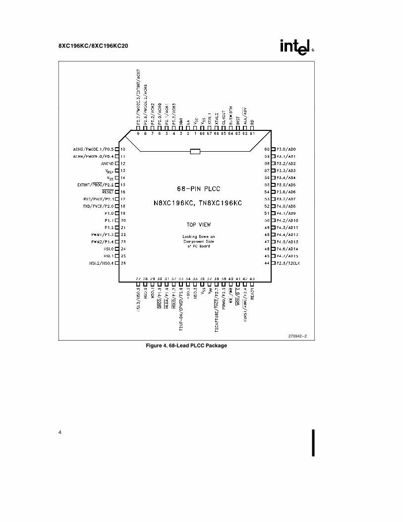
SLAVE PROGRAMMING MODE DATA PROGRAM MODE WITH SINGLE PROGRAM PULSE
270942–27
NOTE:P3.0 must be high (‘‘1’’)
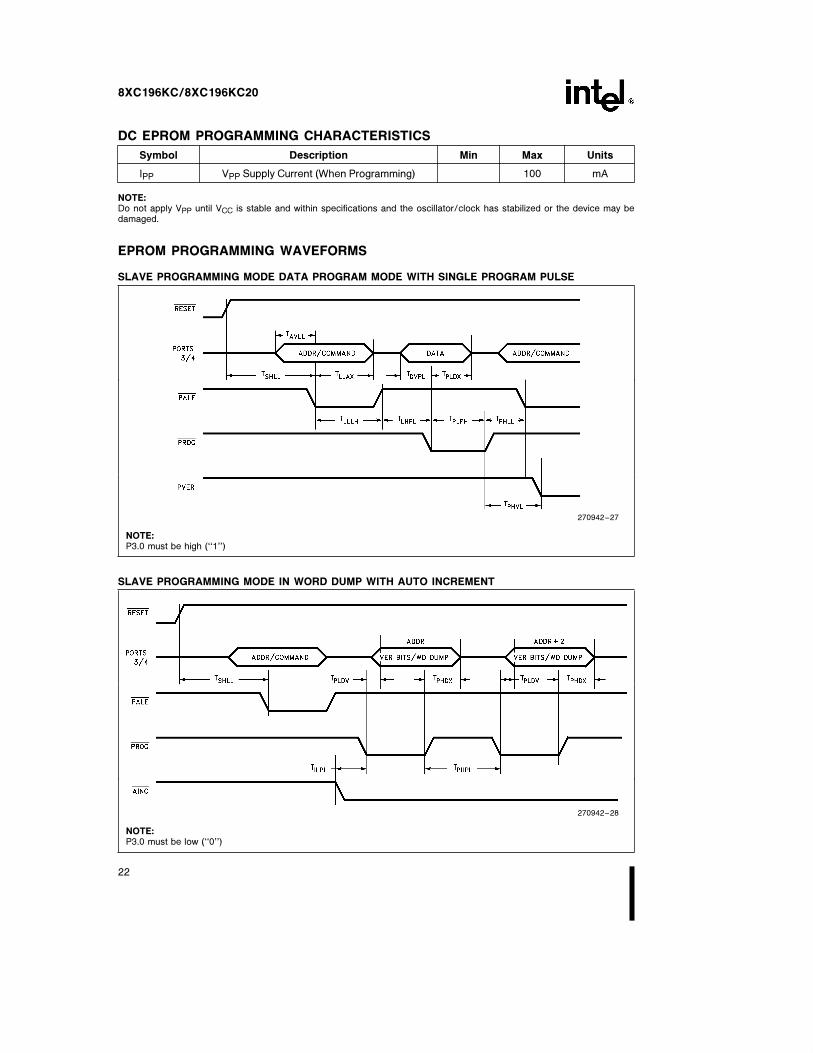
SLAVE PROGRAMMING MODE IN WORD DUMP WITH AUTO INCREMENT
270942–28
NOTE:P3.0 must be low (‘‘0’’)
22

8XC196KC/8XC196KC20
SLAVE PROGRAMMING MODE TIMING IN DATA PROGRAMWITH REPEATED PROG PULSE AND AUTO INCREMENT
270942–29
8XC196KB TO 8XC196KC DESIGNCONSIDERATIONS
1. Memory Map. The 8XC196KC has 512 bytes ofRAM/SFRs and an optional 16K ofROM/OTPROM. The extra 256 bytes of RAM willreside in locations 100H–1FFH and the extra 8Kof ROM/OTPROM will reside in locations4000H–5FFFH. These locations are externalmemory on the 8XC196KB.
2. The CDE pin on the KB has become a VSS pin onthe KC to support 16/20 MHz operation.
3. EPROM programming. The 8XC196KC has a dif-ferent programming algorithm to support 16K ofon-board memory. When performing Run-TimeProgramming, use the section of code in the8XC196KC User’s Guide.
4. ONCE Mode Entry. The ONCE mode is enteredon the 8XC196KC by driving the TXD pin low onthe rising edge of RESET. The TXD pin is heldhigh by a pullup that is specified by IOH1. ThisPullup must not be overridden or the 8XC196KCwill enter the ONCE mode.
5. During the bus HOLD state, the 8XC196KCweakly holds RD, WR, ALE, BHE and INST intheir inactive states. The 8XC196KB only holdsALE in its inactive state.
6. A RESET pulse from the 8XC196KC is 16 statesrather than 4 states as on the 8XC196KB (i.e., awatchdog timer overflow). This provides a longerRESET pulse for other devices in the system.
8XC196KC ERRATA
1. Missed EXTINT on P0.7.
The 80C196KC20 could possibly miss anEXTINT on P0.7. See techbit MC0893.
2. HSIÐMODE divide-by-eight.
See Faxback Ý2192.
3. IPD hump.
See Faxback Ý2311.
23

8XC196KC/8XC196KC20
DATA SHEET REVISION HISTORY
This data sheet is valid for devices with a ‘‘H’’, ‘‘L’’ or ‘‘M’’ at the end of the topside tracking number. Thetopside tracking number consists of nine characters and is the second line on the top side of the device. Datasheets are changed as new device information becomes available. Verify with your local Intel sales office thatyou have the latest version before finalizing a design or ordering devices.
The following are differences between the 270942-004 and 270942-005 datasheets:
1. Removed ‘‘Word Addressable Only’’ from Port 3 and 4 in Table 2.
2. Renamed PVAL to CPVER.
3. Removed TLLYV and TLLGV from the waveform diagrams.
4. Added HSIÐMODE divide-by-eight and IPD hump to 8XC196KC errata.
The following are important differences between the 270942-002 and 270942-004 data sheets:
1. NMI during PTS, QBD port glitch and Divide HOLD/READY erratas were fixed and have been removedfrom the data sheet. The HSI errata is also removed as this is now considered normal operation.
2. Combined 16 and 20 MHz data sheets. Data sheet 270924-001 (20 MHz) is now obsolete.
3. Added 80-lead SQFP package pinout.
4. Added documentation for CLKOUT disable bit.
5. iJA for QFP package was changed to 55§C/W from 42§C/W.
6. iJC for QFP package was changed to 16§C/W from TBD§C/W.
7. TSAM (MIN) in 10-bit mode was changed to 1.0 ms from 3.0 ms.
8. TSAM (MIN) in 8-bit mode was changed to 1.0 ms from 2.0 ms.
9. IIL1 specification for port 2.0 was renamed IIL2.
10. IIL2 (MAX) is changed to TBD from b 6 mA.
11. IIH1 (MAX) is changed to a200 mA from a100 mA.
12. IIH1 test condition changes to VIN e 2.4V from VIN e 5.5V.
13. VHYS is changed to 300 mV from 150 mV.
14. ICC (TYP) at 16 MHz is changed to 65 mA from 50 mA.
15. ICC (MAX) at 16 MHz is changed to 75 mA from 70 mA.
16. ICC (TYP) at 20 MHz is changed to 80 mA from 60 mA.
17. ICC (MAX) at 20 MHz is changed to 92 mA from 86 mA.
18. IIDLE (TYP) at 16 MHz is changed to 17 mA from 15 mA.
19. IIDLE (MAX) at 16 MHz is changed to 25 mA from 30 mA.
20. IIDLE (TYP) at 20 MHz is changed to 21 mA from 15 mA.
21. IIDLE (MAX) at 20 MHz is changed to 30 mA from 35 mA.
22. IPD (TYP) at 16 MHz is changed to 8 mA from 15 mA.
23. IPD (MAX) at 16 MHz is changed to 15 mA from TBD.
24. IPD (TYP) at 20 MHz is changed to 8 mA from 18 mA.
25. IPD (MAX) at 20 MHz is changed to 15 mA from TBD.
26. TCLDV (MAX) is changed to TOSC b45 ns from TOSC b 50 ns.
27. TLLAX (MIN) is changed to TOSC b35 ns from TOSC b 40 ns.
28. TCHWH (MIN) is changed to b5 ns from b10 ns.
29. TRHAX (MIN) is changed to TOSC b 25 ns from TOSC b 30 ns.
30. THALAZ (MAX) is changed to a15 ns from a10 ns.
31. THALBZ (MAX) is changed to a20 ns from a15 ns.
24

8XC196KC/8XC196KC20
32. THAHBV (MAX) is now specified at a15 ns, was formerly unspecified.
33. The TLLYV and TLLGV specifications were removed. These specifications are not required in high-speedsystems designs.
34. Added EXTINT, P0.7 errata to Errata section.
The following are the important differences between the -001 and -002 versions of data sheet 270942.
1. Express and Commercial devices are combined into one data sheet. The Express only data sheet270794-001 is obsolete.
2. Removed KB/KC feature set differences, pin definition table, and SFR locations and bitmaps.
3. Added programming pin function to package drawings and pin descriptions.
4. Changed absolute maximum temperature under bias from 0§C to a70§C to b55§C to a125§C.
5. Replaced VOH2 specification with IOH1 and IIL1 specifications.
6. Added IIH1 specification for NMI pulldown resistors.
7. Added maximum hold latency table.
8. Added external oscillator and external clock circuit drawings.
9. Changed Clock Drive TXHXX and TXLXX Min spec to 20 ns.
10. Fixed Serial Port TXLXH specification.
11. Added 8- and 10-bit mode A/D operating conditions tables.
12. Specified operating range for sample and convert times.
13. Added specification for voltage on analog input pin.
14. Put operating conditions for EPROM programming into tabular format.
25