Embed Size (px)
Citation preview

8k-flash Microcontroller
ATAM894
Rev. 4679D–4BMCU–05/05
Features• 8 K × 8-bit EEPROM• EEPROM Programmable Options• Read Protection for the EEPROM Program Memory• 256 × 4-bit RAM• 2 × 32 × 16-bit Data EEPROM• Up to Seven External/Internal Interrupt Sources• Eight Hardware and Software Interrupt Priorities • 16 Bi-directional I/Os• Wide Supply-voltage Range (1.8V to 6.5V)• Very Low Sleep Current (< 1 µA)• Synchronous Serial Interface (2-wire, 3-wire)• Multifunction Timer/Counter with Prescaler/Interval Timer• Voltage Monitoring Inclusive Lo_BAT Detect• Watchdog, POR and Brown-out Function
1. DescriptionThe ATAM894 is a member of the Atmel’s family of 4-bit single chip microcontrollers with 8K × 8-bit EEPROM program memory. It is based on the 4-K MTP version ATAM893 and fully compatible with this MTP and the ROM versions ATAR090/890 and ATAR092/892.
Figure 1-1. Block Diagram
Voltage monitor External input
MARC4
UTCM
OSC1 OSC2
I/O bus
EEPROM8 K x 8 bit
RAM
4-bit CPU core
256 x 4 bit
VDD
Data direction +alternate function
Data direction +interrupt control
Port 4 Port 5
Data dir. +alt. function
Port 6
Timer 3
Brown-out protect.RESET
Clock managementTimer 1
watchdog timer
Timer 2
Serial interface
Port 1
Por
t 2
Dat
a di
rect
ion
T2O
SD
SC
T3O
T3I
BP10
BP13
BP20/NTE
BP21
BP22
BP23
BP40INT3SC
BP41VMIT2I
BP42T2O
BP43INT3SD
BP50INT6
BP51INT6
BP52INT1
BP53INT1
BP60T3O
BP63T3I
RCoscillators
Crystaloscillators
VMIwith prescaler
SSI
Externalclock input
interval- and
timer/counter
T2I
EEPROM
2 x 32 x 16 bit
Modulator 2
Modulator 3Demodulator
SD
SC
VSS

2. Pin Configuration
Figure 2-1. Pinning SSO24 Package
1
2
3
4
5
6
7
8
10
9
23
18
17
16
14
15
1312
11
24
21
22
19
20
BP52/INT1
BP51/INT6
BP50/INT6
OSC1
OSC2
BP60/T3O
BP40/INT3/SC
BP53/INT1
BP10
VDD
NC
NC
BP41/VMI/T2I
BP23
BP22
BP21
BP20/NTE
BP63/T3I
BP43/INT3/SD
BP42/T2O
BP13
VSS
NC
NC
Table 2-1. Pin Description
Pin Symbol Type Function Alternate Function Reset State
1 NC – Not connected – –
2 NC – Not connected – –
3 VDD – Supply voltage – NA
4 BP40 I/O Bi-directional I/O line of Port 4.0 SC-serial clock or INT3 external interrupt input Input
5 BP53 I/O Bi-directional I/O line of Port 5.3 INT1 external interrupt input Input
6 BP52 I/O Bi-directional I/O line of Port 5.2 INT1 external interrupt input Input
7 BP51 I/O Bi-directional I/O line of Port 5.1 INT6 external interrupt input Input
8 BP50 I/O Bi-directional I/O line of Port 5.0 INT6 external interrupt input Input
9 OSC1 I Oscillator input4-MHz crystal input or 32-kHz crystal input or external clock input or external trimming resistor input
Input
10 OSC2 O Oscillator output4-MHz crystal output or 32-kHz crystal output or external clock input
Input
11 BP60 I/O Bi-directional I/O line of Port 6.0 T3O Timer 3 output Input
12 BP10 I/O Bi-directional I/O line of Port 1.0 – Input
13 BP13 I/O Bi-directional I/O line of Port 1.3 – Input
14 BP63 I/O Bi-directional I/O line of Port 6.3 T3I Timer 3 input Input
15 BP20 I/O Bi-directional I/O line of Port 2.0NTE test mode enable, see section ”Master Reset” on page 12
Input
16 BP21 I/O Bi-directional I/O line of Port 2.1 – Input
17 BP22 I/O Bi-directional I/O line of Port 2.2 – Input
18 BP23 I/O Bi-directional I/O line of Port 2.3 – Input
24679D–4BMCU–05/05
ATAM894

ATAM894
3. IntroductionThe ATAM894 is a member of Atmel’s family of 4-bit single-chip microcontrollers. Instead of ROM it contains EEPROM, RAM, parallel I/O ports, two 8-bit programmable multifunction timer/counters, voltage supervisor, interval timer with watchdog function and a sophisticated on-chip clock generation with integrated RC-, 32-kHz and 4-MHz crystal oscillators.
4. Differences Between ATAM894 and ATARx90/x92
4.1 Program MemoryThe program memory of the MTP device is realized as an EEPROM. The memory size for user programs is 8192 bytes. It is programmed as 258 × 32-byte blocks of data. The implemented LOCK bit function is user selectable and protects the device from unauthorized read out of the program memory.
4.2 Configuration MemoryAn additional area of 64 bytes of the EEPROM is used to store information about the hardware configuration. All the options that are selectable for the ROM versions are available to the user. This includes not only the different port options but also the possibilities to select different capac-itors for OSC1 and OSC2, the option to enable or disable the hardlock for the watchdog, the option to select OSC2 instead of OSC1 as external clock input and the option to enable the external clock monitor as a reset source. Activating the options is performed by the reset cir-cuitry. Reset starts a download sequence to transfer the information from the memory into a shift register (configuration register).
4.3 Data MemoryThe ATAM894 contains an internal data EEPROM that is organized as two pages of 32 × 16 bit. If it is necessary to be compatible with the ROM parts, only one page must be used with the flash part. Also for compatibility reasons the access to the EEPROM is handled via the MCL (serial interface) as in the corresponding ROM parts. A behavioral difference that only needs to be considered for error handling can be seen, when the communication via the MCL is not termi-nated correctly. A missing STOP condition leads to a significantly higher current consumption for the ROM parts compared to the flash parts. A slightly different concept for the read amplifiers of the memory makes the flash part more tolerant in terms of communication errors.
19 BP41 I/O Bi-directional I/O line of Port 4.1VMI voltage monitor input or T2I external clock input Timer 2
Input
20 BP42 I/O Bi-directional I/O line of Port 4.2 T2O Timer 2 output Input
21 BP43 I/O Bi-directional I/O line of Port 4.3 SD serial data I/O or INT3 external interrupt input Input
22 VSS – Circuit ground – Input
23 NC – Not connected – –
24 NC – Not connected – –
Table 2-1. Pin Description (Continued)
Pin Symbol Type Function Alternate Function Reset State
34679D–4BMCU–05/05
4.4 Reset FunctionDuring each reset (power-on or brown-out) the configuration register is reset and reloaded with the data from the configuration memory. This leads to a slightly different behavior compared to the ROM versions. Both devices switch their I/Os to input during reset but the ROM part has the mask selected pull-up or pull-down resistors active while the MTP has them removed until the download is finished.
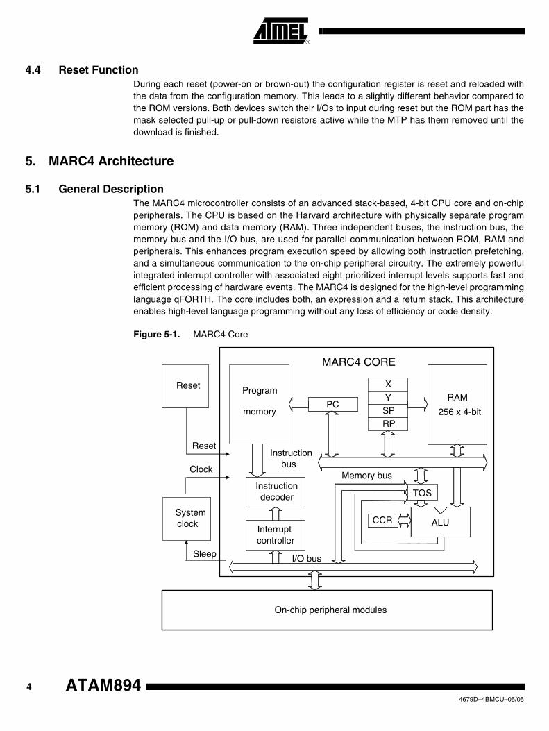
5. MARC4 Architecture
5.1 General DescriptionThe MARC4 microcontroller consists of an advanced stack-based, 4-bit CPU core and on-chip peripherals. The CPU is based on the Harvard architecture with physically separate program memory (ROM) and data memory (RAM). Three independent buses, the instruction bus, the memory bus and the I/O bus, are used for parallel communication between ROM, RAM and peripherals. This enhances program execution speed by allowing both instruction prefetching, and a simultaneous communication to the on-chip peripheral circuitry. The extremely powerful integrated interrupt controller with associated eight prioritized interrupt levels supports fast and efficient processing of hardware events. The MARC4 is designed for the high-level programming language qFORTH. The core includes both, an expression and a return stack. This architecture enables high-level language programming without any loss of efficiency or code density.
Figure 5-1. MARC4 Core
Instruction decoder
CCR
TOS
ALU
RAMPC
RPSP
X
YProgram
256 x 4-bit
MARC4 CORE
Clock
Reset
Sleep
Memory bus
I/O bus
Instruction bus
Reset
System clock
Interruptcontroller
On-chip peripheral modules
memory
44679D–4BMCU–05/05
ATAM894

ATAM894
5.2 Components of MARC4 CoreThe core contains ROM, RAM, ALU, program counter, RAM address registers, instruction decoder and interrupt controller. The following sections describe each functional block in more detail.
5.2.1 Program MemoryThe program memory (EEPROM) is electrically programmable and erasable with the customer application program. The program memory is addressed by a 12-bit wide program counter and an additional ROM bank register, thus predefining a maximum linear adressable program bank size of 4 Kbytes. The upper 2 Kbytes may be exchanged by ROM banking, thus allowing to address a maximum of 10 Kbytes user program. 8 Kbytes of program memory are available within the ATAM894. The lowest user (EEP)ROM address segment is taken up by a 512-byte zero page which contains predefined start addresses for interrupt service routines and special subroutines accessible with single byte instructions (SCALL).
The corresponding memory map is shown in Figure 5-2. Look-up tables of constants can also be held in ROM and are accessed via the MARC4’s built-in table instruction.
Figure 5-2. ROM Map
5.2.1.1 ROM BankingFor customers programming with qFORTH the bank switching is fully supported by the compiler. The MARC4 switches from one ROM bank to another by writing the new bank number to the ROM Bank Register (RBR). Conventional program space (power-up bank) resides in ROM bank 0. Each ROM bank consists of a 2 Kbyte address space whereby the lowest 2 Kbyte, the base bank, is common to all banks, so that addresses between 000h and 7FFh always access the same ROM data (see Figure 5-2). When ROM banking is used, the compiler will, if necessary, insert program code to save and restore the condition of the RBR on bank switching.
5.2.2 RAMThe ATAM894 contains 256 × 4-bit wide static random access memory (RAM). It is used for the expression stack, the return stack and data memory for variables and arrays. The RAM is addressed by any of the four 8-bit wide RAM address registers SP, RP, X and Y.
1F0h1F8h
010h018h
000h008h
020h
1E8h1E0h
SC
ALL
add
ress
es
140h
180h
040h
0C 0h
008h
$AUTOSLEEP
$RESET
INT0
INT1
INT2
INT3
INT4
INT5
INT6
INT71E0h
1C 0h
100h
080h
page
000h
Zero page
Base bank
Bank 1
Bank 2
Bank 4
Bank 3
000h
Port D: 00xxb
FFFh
800h
7FFh
Port D: 11xxb
Port D: 10xxb
Port D: 01xxb
000h
1FFh
54679D–4BMCU–05/05

5.2.2.1 Expression StackThe 4-bit wide expression stack is addressed with the expression Stack Pointer (SP). All arith-metic, I/O and memory reference operations take their operands from, and return their results to the expression stack. The MARC4 performs the operations with the top of stack items (TOS and TOS-1). The TOS register contains the top element of the expression stack and works in the same way as an accumulator. This stack is also used for passing parameters between subrou-tines and as a scratch pad area for temporary storage of data.
5.2.2.2 Return StackThe 12-bit wide return stack is addressed by the Return stack Pointer (RP). It is used for storing return addresses of subroutines, interrupt routines and for keeping loop index counts. The return stack can also be used as a temporary storage area.
The MARC4 instruction set supports the exchange of data between the top elements of the expression stack and the return stack. The two stacks within the RAM have a user definable location and maximum depth.
Figure 5-3. RAM Map
5.2.3 RegistersThe MARC4 controller has seven programmable registers and one condition code register. They are shown in the following programming model.
5.2.3.1 Program Counter (PC)The program counter is a 12-bit register which contains the address of the next instruction to be fetched from the ROM. Instructions currently being executed are decoded in the instruction decoder to determine the internal micro-operations. For linear code (no calls or branches) the program counter is incremented with every instruction cycle. If a branch-, call-, return-instruction or an interrupt is executed, the program counter is loaded with a new address. The program counter is also used with the table instruction to fetch 8-bit wide ROM constants.
RAM
FCh
00h
Autosleep
FFh
03h
04h
X
Y
SP
RP
TOS-1
Expressionstack
Returnstack
Globalvariables
RA
M a
ddre
ss r
egis
ter:
07h
(256 x 4-bit)
Globalvariables
4-bit
TOSTOS-1TOS-2
3 0
SP
Expression stack
Return stack011
12-bit
RP
v
64679D–4BMCU–05/05
ATAM894

ATAM894
Figure 5-4. Programming Model
5.2.3.2 ROM Banking Register (RBR)The ROM banking register is a 4-bit register whereby the ATAM894 only uses 2 bit. This register indicates which ROM bank is presently being addressed. The RBR is accessed with a standard qFORTH peripheral read or write instruction (IN or OUT, port address 'D' hex).
5.2.3.3 RAM Address RegistersThe RAM is addressed with the four 8-bit wide RAM address registers: SP, RP, X and Y. These registers allow access to any of the 256 RAM nibbles.
5.2.3.4 Expression Stack Pointer (SP)The stack pointer contains the address of the next-to-top 4-bit item (TOS-1) of the expression stack. The pointer is automatically pre-incremented if a nibble is moved onto the stack or post-decremented if a nibble is removed from the stack. Every post-decrement operation moves the item (TOS-1) to the TOS register before the SP is decremented. After a reset the stack pointer has to be initialized with “>SP S0” to allocate the start address of the expression stack area.
5.2.3.5 Return Stack Pointer (RP)The return stack pointer points to the top element of the 12-bit wide return stack. The pointer automatically pre-increments if an element is moved onto the stack, or it post-decrements if an element is removed from the stack. The return stack pointer increments and decrements in steps of 4. This means that every time a 12-bit element is stacked, a 4-bit RAM location is left unwritten. This location is used by the qFORTH compiler to allocate 4-bit variables. After a reset the return stack pointer has to be initialized via “>RP FCh”.
TOS
CCR
03
03
07
07
7
011
RP
SP
X
Y
PC
-- B I
Program counter
Return stack pointer
Expression stack pointer
RAM address register (X)
RAM address register (Y)
Top of stack register
Condition code register
Carry/borrow
BranchInterrupt enable
Reserved
07
C
00
RBR
03
ROM banking register----
0
74679D–4BMCU–05/05
5.2.3.6 RAM Address Registers (X and Y)The X and Y registers are used to address any 4-bit item in the RAM. A fetch operation moves the addressed nibble onto the TOS. A store operation moves the TOS to the addressed RAM location. By using either the pre-increment or post-decrement addressing mode arrays in the RAM can be compared, filled or moved.
5.2.3.7 Top Of Stack (TOS)The top of stack register is the accumulator of the MARC4. All arithmetic/logic, memory refer-ence and I/O operations use this register. The TOS register receives data from the ALU, ROM, RAM or I/O bus.
5.2.3.8 Condition Code Register (CCR)The 4-bit wide condition code register contains the branch, the carry and the interrupt enable flag. These bits indicate the current state of the CPU. The CCR flags are set or reset by ALU operations. The instructions SET_BCF, TOG_BF, CCR! and DI allow direct manipulation of the condition code register.
5.2.3.9 Carry/Borrow (C)The carry/borrow flag indicates that the borrowing or carrying out of Arithmetic Logic Unit (ALU) occurred during the last arithmetic operation. During shift and rotate operations, this bit is used as a fifth bit. Boolean operations have no affect on the C-flag.
5.2.3.10 Branch (B)The branch flag controls the conditional program branching. Should the branch flag have been set by a previous instruction, a conditional branch will cause a jump. This flag is affected by arithmetic, logic, shift, and rotate operations.
5.2.3.11 Interrupt Enable (I)The interrupt enable flag globally enables or disables the triggering of all interrupt routines with the exception of the non-maskable reset. After a reset or on executing the DI instruction, the interrupt enable flag is reset, thus disabling all interrupts. The core will not accept any further interrupt requests until the interrupt enable flag has been set again by either executing an EI or SLEEP instruction.
5.2.4 ALUThe 4-bit ALU performs all the arithmetic, logical, shift and rotate operations with the top two ele-ments of the expression stack (TOS and TOS-1) and returns the result to the TOS. The ALU operations affect the carry/borrow and branch flag in the condition code register (CCR).
84679D–4BMCU–05/05
ATAM894

ATAM894
Figure 5-5. ALU Zero-address Operations
5.2.5 I/O BusThe I/O ports and the registers of the peripheral modules are I/O mapped. All communication between the core and the on-chip peripherals takes place via the I/O bus and the associated I/O control. With the MARC4 IN and OUT instructions the I/O bus allows a direct read or write access to one of the 16 primary I/O addresses. More about the I/O access to the on-chip periph-erals is described in the section ”Peripheral Modules” on page 22. The I/O bus is internal and is not accessible by the customer on the final microcontroller device, but it is used as the interface for the MARC4 emulation (see section ”Emulation” on page 92).
5.2.6 Instruction SetThe MARC4 instruction set is optimized for the high level programming language qFORTH. Many MARC4 instructions are qFORTH words. This enables the compiler to generate a fast and compact program code. The CPU has an instruction pipeline allowing the controller to prefetch an instruction from program memory at the same time as the present instruction is being exe-cuted. The MARC4 is a zero address machine, the instructions containing only the operation to be performed and no source or destination address fields. The operations are implicitly per-formed on the data placed on the stack. There are one and two byte instructions which are executed within 1 to 4 machine cycles. A MARC4 machine cycle is made up of two system clock cycles (SYSCL). Most of the instructions are only one byte long and are executed in a single machine cycle. For more information refer to the “MARC4 Programmer’s Guide”.
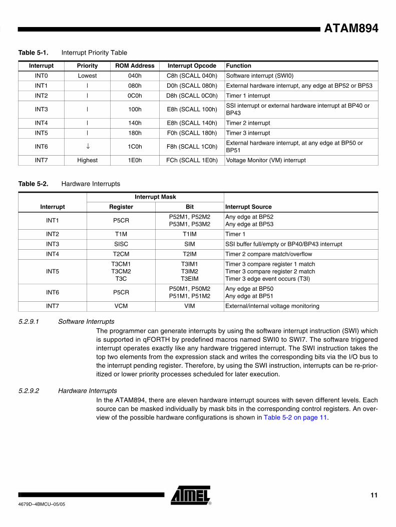
5.2.7 Interrupt StructureThe MARC4 can handle interrupts with eight different priority levels. They can be generated from the internal and external interrupt sources or by a software interrupt from the CPU itself. Each interrupt level has a hard-wired priority and an associated vector for the service routine in the program memory (see Table 5-1 on page 11). The programmer can postpone the processing of interrupts by resetting the interrupt enable flag (I) in the CCR. An interrupt occurrence will still be registered, but the interrupt routine only started after the I flag is set. All interrupts can be masked, and the priority individually software configured by programming the appropriate control register of the interrupting module (see section ”Peripheral Modules” on page 22).
TOS-1
CCR
RAM
TOS-2
SP
TOS-3
TOS
ALUTOS-4
94679D–4BMCU–05/05

5.2.8 Interrupt ProcessingFor processing the eight interrupt levels, the MARC4 includes an interrupt controller with two 8-bit wide “interrupt pending” and “interrupt active” registers. The interrupt controller samples all interrupt requests during every non-I/O instruction cycle and latches these in the interrupt pend-ing register. If no higher priority interrupt is present in the interrupt active register, it signals the CPU to interrupt the current program execution. If the interrupt enable bit is set, the processor enters an interrupt acknowledge cycle. During this cycle a short call (SCALL) instruction to the service routine is executed and the current PC is saved on the return stack. An interrupt service routine is completed with the RTI instruction. This instruction resets the corresponding bits in the interrupt pending/active register and fetches the return address from the return stack to the pro-gram counter. When the interrupt enable flag is reset (triggering of interrupt routines are disabled), the execution of new interrupt service routines is inhibited but not the logging of the interrupt requests in the interrupt pending register. The execution of the interrupt is delayed until the interrupt enable flag is set again. Note that interrupts are only lost if an interrupt request occurs while the corresponding bit in the pending register is still set (i.e., the interrupt service routine is not yet finished).
5.2.9 Interrupt LatencyThe interrupt latency is the time from the occurrence of the interrupt to the interrupt service rou-tine being activated. In MARC4 this is extremely short (taking between 3 to 5 machine cycles depending on the state of the core).
Figure 5-6. Interrupt Handling
7
6
5
4
3
2
1
0
Pri
ori
ty L
evel INT5 active
INT7 active
INT2 pending
SWI0
INT2 active
INT0 pending INT0 active
INT2
RTI
RTIINT5
INT3 active
INT3
RTI
RTI
RTI
INT7
Time
Main /Autosleep
Main/Autosleep
104679D–4BMCU–05/05
ATAM894
ATAM894
5.2.9.1 Software InterruptsThe programmer can generate interrupts by using the software interrupt instruction (SWI) which is supported in qFORTH by predefined macros named SWI0 to SWI7. The software triggered interrupt operates exactly like any hardware triggered interrupt. The SWI instruction takes the top two elements from the expression stack and writes the corresponding bits via the I/O bus to the interrupt pending register. Therefore, by using the SWI instruction, interrupts can be re-prior-itized or lower priority processes scheduled for later execution.
5.2.9.2 Hardware InterruptsIn the ATAM894, there are eleven hardware interrupt sources with seven different levels. Each source can be masked individually by mask bits in the corresponding control registers. An over-view of the possible hardware configurations is shown in Table 5-2 on page 11.
Table 5-1. Interrupt Priority Table
Interrupt Priority ROM Address Interrupt Opcode Function
INT0 Lowest 040h C8h (SCALL 040h) Software interrupt (SWI0)
INT1 | 080h D0h (SCALL 080h) External hardware interrupt, any edge at BP52 or BP53
INT2 | 0C0h D8h (SCALL 0C0h) Timer 1 interrupt
INT3 | 100h E8h (SCALL 100h)SSI interrupt or external hardware interrupt at BP40 or BP43
INT4 | 140h E8h (SCALL 140h) Timer 2 interrupt
INT5 | 180h F0h (SCALL 180h) Timer 3 interrupt
INT6 ↓ 1C0h F8h (SCALL 1C0h)External hardware interrupt, at any edge at BP50 or BP51
INT7 Highest 1E0h FCh (SCALL 1E0h) Voltage Monitor (VM) interrupt
Table 5-2. Hardware Interrupts
Interrupt
Interrupt Mask
Interrupt SourceRegister Bit
INT1 P5CRP52M1, P52M2P53M1, P53M2
Any edge at BP52 Any edge at BP53
INT2 T1M T1IM Timer 1
INT3 SISC SIM SSI buffer full/empty or BP40/BP43 interrupt
INT4 T2CM T2IM Timer 2 compare match/overflow
INT5T3CM1T3CM2
T3C
T3IM1T3IM2T3EIM
Timer 3 compare register 1 match Timer 3 compare register 2 match Timer 3 edge event occurs (T3I)
INT6 P5CRP50M1, P50M2P51M1, P51M2
Any edge at BP50 Any edge at BP51
INT7 VCM VIM External/internal voltage monitoring
114679D–4BMCU–05/05
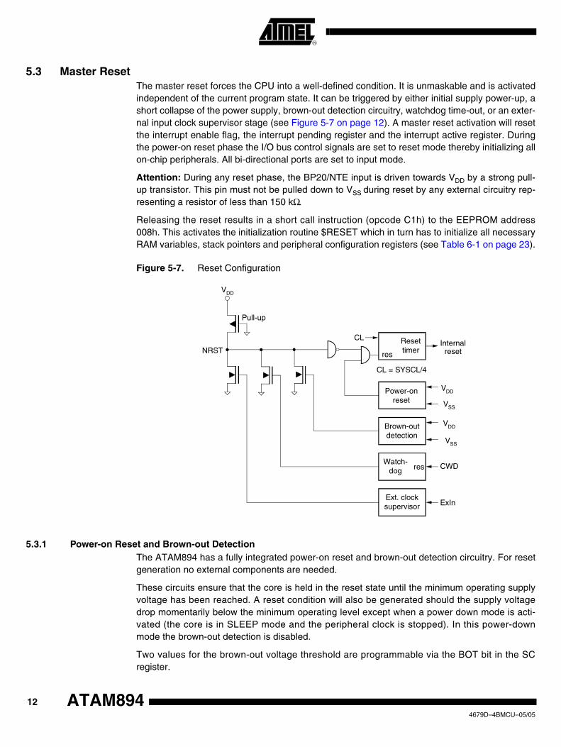
5.3 Master ResetThe master reset forces the CPU into a well-defined condition. It is unmaskable and is activated independent of the current program state. It can be triggered by either initial supply power-up, a short collapse of the power supply, brown-out detection circuitry, watchdog time-out, or an exter-nal input clock supervisor stage (see Figure 5-7 on page 12). A master reset activation will reset the interrupt enable flag, the interrupt pending register and the interrupt active register. During the power-on reset phase the I/O bus control signals are set to reset mode thereby initializing all on-chip peripherals. All bi-directional ports are set to input mode.
Attention: During any reset phase, the BP20/NTE input is driven towards VDD by a strong pull-up transistor. This pin must not be pulled down to VSS during reset by any external circuitry rep-resenting a resistor of less than 150 kΩ.
Releasing the reset results in a short call instruction (opcode C1h) to the EEPROM address 008h. This activates the initialization routine $RESET which in turn has to initialize all necessary RAM variables, stack pointers and peripheral configuration registers (see Table 6-1 on page 23).
Figure 5-7. Reset Configuration
5.3.1 Power-on Reset and Brown-out DetectionThe ATAM894 has a fully integrated power-on reset and brown-out detection circuitry. For reset generation no external components are needed.
These circuits ensure that the core is held in the reset state until the minimum operating supply voltage has been reached. A reset condition will also be generated should the supply voltage drop momentarily below the minimum operating level except when a power down mode is acti-vated (the core is in SLEEP mode and the peripheral clock is stopped). In this power-down mode the brown-out detection is disabled.
Two values for the brown-out voltage threshold are programmable via the BOT bit in the SC register.
Resettimer
VDD
CL
Power-onreset
Internalresetres
CL = SYSCL/4
Brown-outdetection
Watch-dog
CWDres
Ext. clocksupervisor ExIn
Pull-up
NRST
VDD
VSS
VDD
VSS
124679D–4BMCU–05/05
ATAM894

ATAM894
A power-on reset pulse is generated by a VDD rise across the default BOT voltage level (1.7V). A brown-out reset pulse is generated when VDD falls below the brown-out voltage threshold. Two values for the brown-out voltage threshold are programmable via the BOT bit in the SC register. When the controller runs in the upper supply voltage range with a high system clock frequency, the high threshold must be used. When it runs with a lower system clock frequency, the low threshold and a wider supply voltage range may be chosen. For further details, see the electrical specification and the SC register description for BOT programming.
Figure 5-8. Brown-out Detection
Note: BOT = 1, low brown-out voltage threshold 1.7V (is reset value). BOT = 0, high brown-out voltage threshold 2.0V.
5.3.2 Watchdog ResetThe watchdog's function can be enabled at the WDC register and triggers a reset with every watchdog counter overflow. To suppress the watchdog reset, the watchdog counter must be regularly reset by reading the watchdog register address (CWD). The CPU reacts in exactly the same manner as a reset stimulus from any of the above sources.
5.3.3 External Clock SupervisorThe external input clock supervisor function can be enabled if the external input clock is selected within the CM- and SC registers of the clock module. The CPU reacts in exactly the same man-ner as a reset stimulus from any of the above sources.
5.4 Voltage MonitorThe voltage monitor consists of a comparator with an internal voltage reference. It is used to supervise the supply voltage or an external voltage at the VMI pin. The comparator for the sup-ply voltage has three internal programmable thresholds: one lower threshold (2.2V), one middle threshold (2.6 V) and one higher threshold (3.0V). For external voltages at the VMI pin, the com-parator threshold is set to VBG = 1.3V. The VMS bit indicates if the supervised voltage is below (VMS = 0) or above (VMS = 1) this threshold. An interrupt can be generated when the VMS bit is set or reset to detect a rising or falling slope. A voltage monitor interrupt (INT7) is enabled when the interrupt mask bit (VIM) is reset in the VMC register.
VDD
CPUReset
t
BOT = 1
2.0 V1.7 V
BOT = 0
td = 1.5 ms (typically)
tdtd
td
CPUReset
134679D–4BMCU–05/05
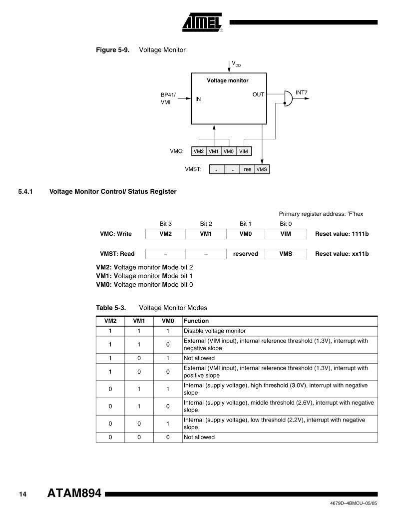
Figure 5-9. Voltage Monitor
5.4.1 Voltage Monitor Control/ Status Register
VM2: Voltage monitor Mode bit 2 VM1: Voltage monitor Mode bit 1 VM0: Voltage monitor Mode bit 0
VDD
VM2
Voltage monitor
VM1 VM0 VIM
VMS - - res
OUTIN
BP41/VMI
INT7
VMC:
VMST:
Primary register address: ’F’hex
Bit 3 Bit 2 Bit 1 Bit 0
VMC: Write VM2 VM1 VM0 VIM Reset value: 1111b
VMST: Read – – reserved VMS Reset value: xx11b
Table 5-3. Voltage Monitor Modes
VM2 VM1 VM0 Function
1 1 1 Disable voltage monitor
1 1 0External (VIM input), internal reference threshold (1.3V), interrupt with negative slope
1 0 1 Not allowed
1 0 0External (VMI input), internal reference threshold (1.3V), interrupt with positive slope
0 1 1Internal (supply voltage), high threshold (3.0V), interrupt with negative slope
0 1 0Internal (supply voltage), middle threshold (2.6V), interrupt with negative slope
0 0 1Internal (supply voltage), low threshold (2.2V), interrupt with negative slope
0 0 0 Not allowed
144679D–4BMCU–05/05
ATAM894

ATAM894
VIM Voltage Interrupt Mask bit
VIM = 0, voltage monitor interrupt is enabled VIM = 1, voltage monitor interrupt is disabled
VMS Voltage Monitor Status bit
VMS = 0, the voltage at the comparator input is below VRef VMS = 1, the voltage at the comparator input is above VRef
Figure 5-10. Internal Supply Voltage Supervisor
Figure 5-11. External Input Voltage Supervisor
5.5 Clock Generation
5.5.1 Clock ModuleThe ATAM894 contains a clock module with 4 different internal oscillator types: two RC-oscilla-tors, one 4-MHz crystal oscillator and one 32-kHz crystal oscillator. The pins OSC1 and OSC2 are the interface to connect a crystal either to the 4-MHz, or to the 32-kHz crystal oscillator. OSC1 can be used as input for external clocks or to connect an external trimming resistor for the RC-oscillator 2. All necessary circuitry except the crystal and the trimming resistor is integrated on-chip. One of these oscillator types or an external input clock can be selected to generate the system clock (SYSCL).
In applications that do not require exact timing, it is possible to use the fully integrated RC-oscil-lator 1 without any external components. The RC-oscillator 1 center frequency tolerance is better than ±50%. The RC-oscillator 2 is a trimmable oscillator whereby the oscillator frequency can be trimmed with an external resistor attached between OSC1 and VDD. In this configuration, the RC-oscillator 2 frequency can be maintained stable to within a tolerance of ±15% over the full operating temperature and voltage range.
VDD
Low thresholdMiddle thresholdHigh threshold
VMS = 1
Low thresholdMiddle thresholdHigh threshold
VMS = 0
3.0 V2.6 V2.2 V
1.3 V
VMI
VMS = 1
VMS = 0
Positive slope
Negative slope
VMS = 1
VMS = 0
Interrupt negative slope
Interrupt positive slope
Internal reference level
t
154679D–4BMCU–05/05
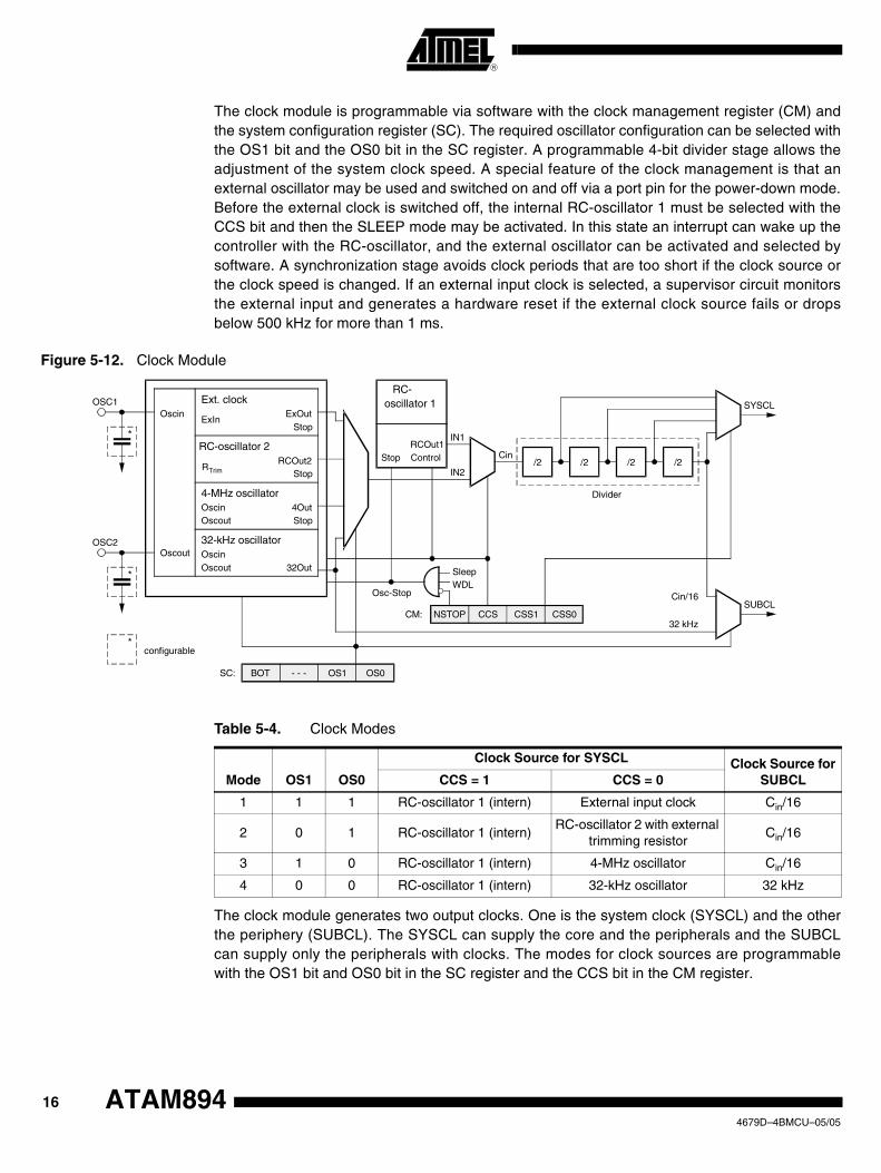
The clock module is programmable via software with the clock management register (CM) and the system configuration register (SC). The required oscillator configuration can be selected with the OS1 bit and the OS0 bit in the SC register. A programmable 4-bit divider stage allows the adjustment of the system clock speed. A special feature of the clock management is that an external oscillator may be used and switched on and off via a port pin for the power-down mode. Before the external clock is switched off, the internal RC-oscillator 1 must be selected with the CCS bit and then the SLEEP mode may be activated. In this state an interrupt can wake up the controller with the RC-oscillator, and the external oscillator can be activated and selected by software. A synchronization stage avoids clock periods that are too short if the clock source or the clock speed is changed. If an external input clock is selected, a supervisor circuit monitors the external input and generates a hardware reset if the external clock source fails or drops below 500 kHz for more than 1 ms.
Figure 5-12. Clock Module
The clock module generates two output clocks. One is the system clock (SYSCL) and the other the periphery (SUBCL). The SYSCL can supply the core and the peripherals and the SUBCL can supply only the peripherals with clocks. The modes for clock sources are programmable with the OS1 bit and OS0 bit in the SC register and the CCS bit in the CM register.
Ext. clock
ExInExOut
Stop
RC-oscillator 2RCOut2
StopRTrim
4-MHz oscillator4OutStop
OscinOscout
Oscin
Oscout32-kHz oscillator
32OutOscinOscout
RC-oscillator 1
RCOut1ControlStop
IN1
IN2
Cin/2 /2 /2 /2
Divider
SleepWDL
Osc-Stop
NSTOP CCS CSS1 CSS0CM:
BOT - - - OS1 OS0
SUBCL
SYSCL
SC:
*
OSC1
*
OSC2
*configurable
Cin/16
32 kHz
Table 5-4. Clock Modes
Mode OS1 OS0
Clock Source for SYSCL Clock Source for SUBCLCCS = 1 CCS = 0
1 1 1 RC-oscillator 1 (intern) External input clock Cin/16
2 0 1 RC-oscillator 1 (intern)RC-oscillator 2 with external
trimming resistorCin/16
3 1 0 RC-oscillator 1 (intern) 4-MHz oscillator Cin/16
4 0 0 RC-oscillator 1 (intern) 32-kHz oscillator 32 kHz
164679D–4BMCU–05/05
ATAM894

ATAM894
5.5.2 Oscillator Circuits and External Clock Input StageThe ATAM894 series consists of four different internal oscillators: two RC-oscillators, one 4-MHz crystal oscillator, one 32-kHz crystal oscillator and one external clock input stage.
5.5.2.1 RC-oscillator 1 Fully IntegratedFor timing insensitive applications, it is possible to use the fully integrated RC-oscillator 1. It operates without any external components and saves additional costs. The RC-oscillator 1 cen-ter frequency tolerance is better than ±50% over the full temperature and voltage range. The basic center frequency of the RC-oscillator 1 is fO ≈ 4.0 MHz. The RC-oscillator 1 is selected by default after power-on reset.
Figure 5-13. RC-oscillator 1
5.5.2.2 External Input ClockThe OSC1 or OSC2 can be driven by an external clock source provided it meets the specified duty cycle, rise and fall times and input levels. Additionally, the external clock stage contains a supervisory circuit for the input clock. The supervisor function is controlled via the OS1, OS0 bit in the SC register and the CCS bit in the CM register. If the external input clock is missing for more than 1 ms and CCS = 0 is set in the CM register, the supervisory circuit generates a hard-ware reset.
Figure 5-14. External Input Clock
RC-oscillator 1
RcOut1
Stop
Control
RcOut1
Osc-Stop
Ext. input clock
ExOut
Stop
Ext.Clock
RcOut1
Osc-StopExIn
CCS
Res
OSC1
OSC2 Clock monitorExt.Clock
or
174679D–4BMCU–05/05

5.5.2.3 RC-oscillator 2 with External Trimming ResistorThe RC-oscillator 2 is a high resolution trimmable oscillator whereby the oscillator frequency can be trimmed with an external resistor between OSC1 and VDD. In this configuration, the RC-oscil-lator 2 frequency can be maintained stable with a tolerance of ±15% over the full operating temperature and a voltage range VDD from 2.5V to 6.0V.
For example: An output frequency at the RC-oscillator 2 of 2 MHz can be obtained by connect-ing a resistor Rext = 360 kΩ (see Figure 5-15).
Figure 5-15. RC-oscillator 2
5.5.2.4 4-MHz OscillatorThe ATAM894 4-MHz oscillator options need a crystal or ceramic resonator connected to the OSC1 and OSC2 pins to establish oscillation. All the necessary oscillator circuitry, with the exception of the actual crystal, resonator, C3 and C4 are integrated on-chip.
Figure 5-16. 4-MHz Crystal Oscillator
Note: Both, the 4-MHz and the 32-kHz crystal oscillator, use an integrated 14 stage divider circuit to sta-bilize oscillation before the oscillator output is used as system clock. This results in an additional delay of about 4 ms for the 4-MHz crystal and about 500 ms for the 32-kHz crystal.
Table 5-5. Supervisor Function Control Bits
OS1 OS0 CCS Supervisor Reset Output (Res)
1 1 0 Enable
1 1 1 Disable
x 0 x Disable
RC-oscillator 2
RcOut2
Stop
RcOut2
Osc-StopRTrim
OSC1
OSC2
Rext
VDD
4-MHzoscillator
4Out4Out
OSC1
OSC2
*
Oscin
C1
*
C2
Oscout
XTAL4 MHz
*
configurable
StopOsc-Stop
184679D–4BMCU–05/05
ATAM894

ATAM894
Figure 5-17. Ceramic Resonator
Note: Both, the 4-MHz and the 32-kHz crystal oscillator, use an integrated 14 stage divider circuit to sta-bilize oscillation before the oscillator output is used as system clock. This results in an additional delay of about 4 ms for the 4-MHz crystal and about 500 ms for the 32-kHz crystal.
5.5.2.5 32-kHz OscillatorSome applications require long-term time keeping or low resolution timing. In this case, an on-chip, low power 32-kHz crystal oscillator can be used to generate both the SUBCL and the SYSCL. In this mode, power consumption is greatly reduced. The 32-kHz crystal oscillator can not be stopped while the power-down mode is in operation.
Figure 5-18. 32-kHz Crystal Oscillator
Note: Both, the 4-MHz and the 32-kHz crystal oscillator, use an integrated 14 stage divider circuit to sta-bilize oscillation before the oscillator output is used as system clock. This results in an additional delay of about 4 ms for the 4-MHz crystal and about 500 ms for the 32-kHz crystal.
5.5.3 Clock ManagementThe clock management register controls the system clock divider and synchronization stage. Writing to this register triggers the synchronization cycle.
4-MHzoscillator
4Out
Stop
4Out
Osc-Stop
OSC1
OSC2
*
Oscin
C1
*
C2
Oscout
Cer.Res
*
configurable
C3
C4
32-kHzoscillator
32Out32Out
OSC1
OSC2
*
Oscin
C1
*
C2
Oscout
XTAL32 kHz
*
configurable
194679D–4BMCU–05/05

5.5.3.1 Clock Management Register (CM)
5.5.3.2 System Configuration Register (SC)
Auxiliary register address: '3'hex
Bit 3 Bit 2 Bit 1 Bit 0
CM: NSTOP CCS CSS1 CSS0 Reset value: 1111b
NSTOPNot STOP peripheral clock NSTOP = 0, stops the peripheral clock while the core is in SLEEP mode NSTOP = 1, enables the peripheral clock while the core is in SLEEP mode
CCS
Core Clock Select CCS = 1, the internal RC-oscillator 1 generates SYSCL CCS = 0, the 4-MHz crystal oscillator, the 32-kHz crystal oscillator, an external clock source or the RC-oscillator 2 with the external resistor at OSC1 generates SYSCL dependent on the setting of OS0 and OS1 in the system configuration register
CSS1 Core Speed Select 1
CSS0 Core Speed Select 0
Table 5-6. Core Speed Select
CSS1 CSS0 Divider Note
0 0 16
1 1 8 Reset value
1 0 4
0 1 2
Primary register address: '3'hex
Bit 3 Bit 2 Bit 1 Bit 0
SC: write BOT – OS1 OS0 Reset value: 1x11b
BOTBrown-Out Threshold BOT = 1, low brown-out voltage threshold (1.65V) BOT = 0, high brown-out voltage threshold (1.95V)
OS1 Oscillator Select 1
OS0 Oscillator Select 0
204679D–4BMCU–05/05
ATAM894

ATAM894
Note: If the bit CCS = 0 in the CM-register the RC-oscillator 1 always stops.
5.6 Power-down ModesThe sleep mode is a shut-down condition which is used to reduce the average system power consumption in applications where the microcontroller is not fully utilized. In this mode, the sys-tem clock is stopped. The sleep mode is entered via the SLEEP instruction. This instruction sets the interrupt enable bit (I) in the condition code register to enable all interrupts and stops the core. During the sleep mode the peripheral modules remain active and are able to generate interrupts. The microcontroller exits the sleep mode by carrying out any interrupt or a reset.
The sleep mode can only be kept when none of the interrupt pending or active register bits are set. The application of the $AUTOSLEEP routine ensures the correct function of the sleep mode. For standard applications use the $AUTOSLEEP routine to enter the power-down mode. Using the SLEEP instruction instead of the $AUTOSLEEP following an I/O instruction requires the insertion of 3 non-I/O instruction cycles (for example NOP, NOP, NOP) between the IN or OUT command and the SLEEP command.
The total power consumption is directly proportional to the active time of the microcontroller. For a rough estimation of the expected average system current consumption, the following formula should be used:
IDD depends on VDD and fsyscl
The ATAM894 has various power-down modes. During the sleep mode the clock for the MARC4 core is stopped. With the NSTOP bit in the clock management register (CM) it is programmable if the clock for the on-chip peripherals is active or stopped during the sleep mode. If the clock for the core and the peripherals is stopped the selected oscillator is switched off. An exception is the 32-kHz oscillator, if it is selected it runs continuously independent of the NSTOP bit. If the oscil-lator is stopped or the 32-kHz oscillator is selected, power consumption is extremely low.
Table 5-7. Oscillator Select
Mode OS1 OS0 Input for SUBCL Selected Oscillators
1 1 1 Cin/16 RC-oscillator 1 and external input clock
2 0 1 Cin/16 RC-oscillator 1 and RC-oscillator 2
3 1 0 Cin/16 RC-oscillator 1 and 4-MHz crystal oscillator
4 0 0 32 kHz RC-oscillator 1 and 32-kHz crystal oscillator
Table 5-8. Power-down Modes
Mode CPU CoreOsc-
Stop(1)Brown-out Function
RC-Oscillator 1RC-Oscillator 2
4-MHz Oscillator32-kHz
OscillatorExternal
Input Clock
Active RUN NO Active RUN RUN YES
Power-down SLEEP NO Active RUN RUN YES
SLEEP SLEEP YES STOP STOP RUN STOP
Note: 1. Osc-Stop = SLEEP and NSTOP and WDL
Itotal VDD,fsyscl( ) ISleep IDD
tactive
ttotal--------------×⎝ ⎠
⎛ ⎞+=
214679D–4BMCU–05/05

6. Peripheral Modules
6.1 Addressing Peripherals Accessing the peripheral modules takes place via the I/O bus (see Figure 6-1). The IN or OUT instructions allow direct addressing of up to 16 I/O modules. A dual register addressing scheme has been adopted to enable direct addressing of the primary register. To address the auxiliary register, the access must be switched with an auxiliary switching module. Thus, a single IN (or OUT) to the module address will read (or write into) the module primary register. Accessing the auxiliary register is performed with the same instruction preceded by writing the module address into the auxiliary switching module. Byte wide registers are accessed by multiple IN- (or OUT-) instructions. For more complex peripheral modules, with a larger number of registers, extended addressing is used. In this case a bank of up to 16 subport registers are indirectly addressed with the subport address. The first OUT-instruction writes the subport address to the subaddress register, the second IN- or OUT-instruction reads data from or writes data to the addressed subport.
Figure 6-1. Example of I/O Addressing
Subaddress Reg.
Subport FH
I/O bus
Aux. Reg.Bank ofPrimary Regs.
Primary Reg.
(Address Pointer)
Auxiliary SwitchModule
Indirect Subport Access
to other modules
1
2
(Subport Register Write)
3
4
5
1
2 3
6
6
4
5
Example ofqFORTHProgramCode
1
2
4
5
3
6
Addr. (ASW) = Auxililiary Switch Module Address
1
2
2
1
2
2
4
5
5
(Auxiliary Register Write)
Module ASW Module M1 Module M2 Module M3
Subport EH
Primary Reg.Primary Reg.
Subport 1
Subport 0
Dual Register Access Single Register Access
Addr. (SPort) Addr. (M1) OUT
SPort_Data Addr. (M1) OUT
(Subport Register Read)
Addr. (SPort) Addr. (M1) OUT
Addr. (M1) IN
(Subport Register Write Byte)
Addr. (SPort) Addr. (M1) OUT
SPort_Data (lo) Addr. (M1) OUT
SPort_Data (hi) Addr. (M1) OUT
(Subport Register Read Byte)
Addr. (SPort) Addr. (M1) OUT
Addr. (M1) IN (hi)
Addr. (M1) IN (lo)
(Primary Register Write)
Prim._Data Addr. (M2) OUT
Addr. (M2) Addr. (ASW) OUT
Aux._Data Addr. (M2) OUT
(Primary Register Read)
Addr. (M2) IN
(Auxiliary Register Read )
Addr. (M2) Addr. (ASW) OUT
Addr. (M2) IN
(Auxiliary Register Write Byte)
Addr. (M2) Addr. (ASW) OUT
Aux._Data (lo) Addr. (M2) OUT
Aux._Data (hi) Addr. (M2) OUT
(Primary Register Write)
Prim._Data Addr. (M3) OUT
(Primary Register Read)
Addr. (M3) IN
Addr. (Mx) = Module Mx Address
Addr. (SPort) = Subport Address
Prim._Data = Data to be written into Primary Register
Aux._Data = Data to be written into Auxiliary Register
Aux._Data (lo) = Data to be written into Auxiliary Register (low nibble)
Aux._Data (hi) = Data to be written into Auxiliary Register (high nibble)
SPort_Data (lo) = Data to be written into Subport (low nibble)
SPort_Data (hi) = Data to be written into Subport (high nibble)
(lo) = SPort_Data (low nibble)
(hi) = SPort_Data (high nibble)
224679D–4BMCU–05/05
ATAM894

ATAM894
Table 6-1. Peripheral Addresses
Port Address Name Write/Read Reset Value Register FunctionModule
TypeSee
Page
1 P1DAT W/R 1xx1b Port 1 - data register/input data M3 page 24
2 P2DAT W/R 1111b Port 2 - data register/pin data M2 page 26
Auxiliary P2CR W 1111b Port 2 - control register page 26
3 SC W 1x11b System configuration register M3 page 20
CWD R xxxxb Watchdog reset M3 page 13
Auxiliary CM W 1111b Clock management register M2 page 20
4 P4DAT W/R 1111b Port 4 - data register/pin data M2 page 29
Auxiliary P4CR W 1111 1111b Port 4 - control register (byte) page 29
5 P5DAT W/R 1111b Port 5 - data register/pin data M2 page 28
Auxiliary P5CR W 1111 1111b Port 5 - control register (byte) page 28
6 P6DAT W/R 1xx1b Port 6 - data register/pin data M2 page 30
Auxiliary P6CR W 1111b Port 6 - control register (byte) page 30
7 T12SUB W – Data to Timer 1/2 subport M1 page 22
Subport address
0 T2C W 0000b Timer 2 control register M1 page 43
1 T2M1 W 1111b Timer 2 mode register 1 M1 page 43
2 T2M2 W 1111b Timer 2 mode register 2 M1 page 45
3 T2CM W 0000b Timer 2 compare mode register M1 page 45
4 T2CO1 W 1111b Timer 2 compare register 1 M1 page 46
5 T2CO2 W 1111 1111b Timer 2 compare register 2 (byte) M1 page 46
6 – – – Reserved
7 – – – Reserved
8 T1C1 W 1111b Timer 1 control register 1 M1 page 33
9 T1C2 W x111b Timer 1 control register 2 M1 page 34
A WDC W 1111b Watchdog control register M1 page 34
B-F Reserved
8 ASW W 1111b Auxiliary/switch register ASW page 22
9 STB W xxxx xxxxb Serial transmit buffer (byte) M2 page 70
SRB R xxxx xxxxb Serial receive buffer (byte) page 71
Auxiliary SIC1 W 1111b Serial interface control register 1 page 68
A SISC W/R 1x11b Serial interface status/control register M2 page 70
Auxiliary SIC2 W 1111b Serial interface control register 2 page 69
B T3SUB W/R – Data to/from Timer 3 subport M1 page 22
Subport address
0 T3M W 1111b Timer 3 mode register M1 page 55
1 T3CS W 1111b Timer 3 clock select register M1 page 57
2 T3CM1 W 0000b Timer 3 compare mode register 1 M1 page 58
3 T3CM2 W 0000b Timer 3 compare mode register 2 M1 page 58
4 T3CO1 W 1111 1111b Timer 3 compare register 1 (byte) M1 page 59
4 T3CP R xxxx xxxxb Timer 3 capture register (byte) M1 page 59
5 T3CO2 W 1111 1111b Timer 3 compare register 2 (byte) M1 page 59
6 W 1111b Reserved
7-F – Reserved
C T3C W 0000b Timer 3 control register M3 page 56
T3ST R x000b Timer 3 status register M3 page 56
D, E --- – Reserved
F VMC W 1111b Voltage monitor control register M3 page 14
VMST R xx11b Voltage monitor status register M3 page 14
234679D–4BMCU–05/05

6.2 Bi-directional PortsWith the exception of Port 1 and Port 6, all other ports (2, 4 and 5) are 4 bits wide. Port 1 and Port 6 have a data width of 2 bits (bit 0 and bit 3). All ports may be used for data input or output. All ports are equipped with Schmitt trigger inputs and a variety of mask options for open drain, open source, full complementary outputs, pull-up and pull-down transistors. All Port Data Regis-ters (PxDAT) are I/O mapped to the primary address register of the respective port address and the Port Control Register (PxCR), to the corresponding auxiliary register.
There are five different directional ports available:
Port 1 2-bit wide bi-directional ports with automatic full bus width direction switching
Port 2 4-bit wide bit-wise-programmable I/O port
Port 5 4-bit wide bit-wise-programmable bi-directional port with optional strong pull-ups and programmable interrupt logic
Port 4 4-bit wide bit-wise-programmable bi-directional port also provides the I/O interface to Timer 2, SSI, voltage monitor input and external interrupt input
Port 6 2-bit wide bit-wise-programmable bi-directional port also provides the I/O interface to Timer 3 and external interrupt input
6.2.1 Bi-directional Port 1In Port 1 the data direction register is not independently software programmable, the direction of the complete port being switched automatically when an I/O instruction occurs (see Figure 6-2 on page 25). The port is switched to output mode via an OUT instruction and to input via an IN instruction. The data written to a port will be stored into the output data latches and appears immediately at the port pin following the OUT instruction. After RESET all output latches are set to '1' and the port is switched to input mode. An IN instruction reads the condition of the associ-ated pins.
Note: Care must be taken when switching the bi-directional port from output to input. The capacitive pin loading at this port in conjunction with the high resistance pull-ups may cause the CPU to read the contents of the output data register rather than the external input state. To avoid this, one of the following programming techniques should be used: Use two IN-instructions and DROP the first data nibble. The first IN switches the port from output to input and the DROP removes the first invalid nibble. The second IN reads the valid pin state. Use an OUT-instruction followed by an IN-instruction. Via the OUT-instruction, the capacitive load is charged or discharged depending on the optional pull-up/pull-down configuration. Write a ’1’ for pins with pull-up resistors and a '0' for pins with pull-down resistors.
244679D–4BMCU–05/05
ATAM894
ATAM894
Figure 6-2. Bi-directional Port 1
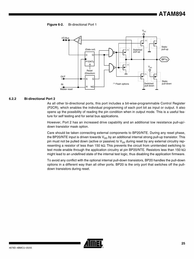
6.2.2 Bi-directional Port 2As all other bi-directional ports, this port includes a bit-wise-programmable Control Register (P2CR), which enables the individual programming of each port bit as input or output. It also opens up the possibility of reading the pin condition when in output mode. This is a useful fea-ture for self testing and for serial bus applications.
However, Port 2 has an increased drive capability and an additional low resistance pull-up/-down transistor mask option.
Care should be taken connecting external components to BP20/NTE. During any reset phase, the BP20/NTE input is driven towards VDD by an additional internal strong pull-up transistor. This pin must not be pulled down (active or passive) to VSS during reset by any external circuitry rep-resenting a resistor of less than 150 kΩ. This prevents the circuit from unintended switching to test mode enable through the application circuitry at pin BP20/NTE. Resistors less than 150 kΩmight lead to an undefined state of the internal test logic, thus disabling the application firmware.
To avoid any conflict with the optional internal pull-down transistors, BP20 handles the pull-down options in a different way than all other ports. BP20 is the only port that switches off the pull-down transistors during reset.
OUT
IN
Reset
I/O Bus
D
R
S
Q
Q
NQ
R
Master reset
P1DATy
(Data out)
(Direction)
BP1y
Switched
Switched
(1)
(1) Flash options
VDD
Staticpull-up
Staticpull-down
pull-up
pull-down
(1)
(1)
(1)
VDD
254679D–4BMCU–05/05

Figure 6-3. Bi-directional Port 2
6.2.2.1 Port 2 Data Register (P2DAT)
Note: * Bit 3 = MSB, Bit 0 = LSB
6.2.2.2 Port 2 Control Register (P2CR)
Note: Value 1111b means all pins in input mode
Master reset
Q
Q
BP2y
(1) Flash options
P2DATy
P2CRy
I/O Bus
D
I/O Bus
I/O Bus
Switchedpull-up Static
Pull-up
(Data out)
(Direction)
SD
(1)S
StaticPull-down
Switchedpull-down
VDD
VDD
(1) (1)
(1)
(1) (1)
Primary register address: '2'hex
Bit 3* Bit 2 Bit 1 Bit 0
P2DAT P2DAT3 P2DAT2 P2DAT1 P2DAT0 Reset value: 1111b
Auxiliary register address: '2'hex
Bit 3 Bit 2 Bit 1 Bit 0
P2CR P2CR3 P2CR2 P2CR1 P2CR0 Reset value: 1111b
Table 6-2. Port 2 Control Register
Code3 2 1 0 Function
x x x 1 BP20 in input mode
x x x 0 BP20 in output mode
x x 1 x BP21 in input mode
x x 0 x BP21 in output mode
x 1 x x BP22 in input mode
x 0 x x BP22 in output mode
1 x x x BP23 in input mode
0 x x x BP23 in output mode
264679D–4BMCU–05/05
ATAM894

ATAM894
6.2.3 Bi-directional Port 5As all other bi-directional ports, this port includes a bit-wise-programmable Control Register (P5CR), which allows the individual programming of each port bit as input or output. It also opens up the possibility of reading the pin condition when in output mode. This is a useful fea-ture for self-testing and for serial bus applications.
The port pins can also be used as external interrupt inputs (see Figure 6-4 on page 27 and Fig-ure 6-5 on page 27). The interrupts (INT1 and INT6) can be masked or independently configured to trigger on either edge. The interrupt configuration and port direction is controlled by the Port 5 Control Register (P5CR). An additional low resistance pull-up/-down transistor mask option pro-vides an internal bus pull-up for serial bus applications.
The Port 5 Data Register (P5DAT) is I/O mapped to the primary address register of address '5'h and the Port 5 Control Register (P5CR) to the corresponding auxiliary register. The P5CR is a byte-wide register and is configured by writing first the low nibble and then the high nibble (see section ”Addressing Peripherals” on page 22).
Figure 6-4. Bi-directional Port 5
Figure 6-5. Port 5 External Interrupts
Master reset
Q
VDD
BP5y
(1) Flash options
P5DATy
I/O Bus
D
IN enable
I/O Bus(1)
Switchedpull-up
Switchedpull-down
Staticpull-up
(Data out)
S
Staticpull-down
VDD
VDD(1)
(1) (1)
(1) (1)
Bidir. Port
Data in
IN_Enable
BP53
P53M2P53M1P52M2P52M1P51M2P51M1P50M2P50M1
Decoder Decoder Decoder Decoder
Bidir. Port
Data in
IN_Enable
BP52
I/O-bus
Bidir. Port
Data in
IN_Enable
BP5
I/O-bus
Bidir. Port
Data in
IN_Enable
BP5
INT1 INT6
P5CR:1376
274679D–4BMCU–05/05

6.2.3.1 Port 5 Data Register (P5DAT)
6.2.3.2 Port 5 Control Register (P5CR) Byte Write
P5xM2, P5xM1 – Port 5x Interrupt Mode/Direction Code
6.2.4 Bi-directional Port 4The bi-directional Port 4 is a bit-wise configurable I/O port and provides the external pins for the Timer 2, SSI and the voltage monitor input (VMI). As a normal port, it performs in exactly the same way as bi-directional Port 2 (see Figure 6-3 on page 26). Two additional multiplexes allow data and port direction control to be passed over to other internal modules (Timer 2, VM or SSI). The I/O pins for the SC and SD lines have an additional mode to generate an SSI-interrupt.
All four Port 4 pins can be individually switched by the P4CR register. Figure 6-6 on page 29shows the internal interfaces to bi-directional Port 4.
Primary register address: '5'hex
Bit 3 Bit 2 Bit 1 Bit 0
P5DAT P5DAT3 P5DAT2 P5DAT1 P5DAT0 Reset value: 1111b
Auxiliary register address: '5'hex
Bit 3 Bit 2 Bit 1 Bit 0
P5CR First write cycle P51M2 P51M1 P50M2 P50M1 Reset value: 1111b
Bit 7 Bit 6 Bit 5 Bit 4
Second write cycle
P53M2 P53M1 P52M2 P52M1 Reset value: 1111b
Table 6-3. Port 5 Control Register
Auxiliary Address: '5'hex First Write Cycle Second Write Cycle
Code3 2 1 0 Function
Code3 2 1 0 Function
x x 1 1 BP50 in input mode – interrupt disabled x x 1 1 BP52 in input mode – interrupt disabled
x x 0 1 BP50 in input mode – rising edge interrupt x x 0 1 BP52 in input mode – rising edge interrupt
x x 1 0 BP50 in input mode – falling edge interrupt x x 1 0 BP52 in input mode – falling edge interrupt
x x 0 0 BP50 in output mode – interrupt disabled x x 0 0 BP52 in output mode – interrupt disabled
1 1 x x BP51 in input mode – interrupt disabled 1 1 x x BP53 in input mode – interrupt disabled
0 1 x x BP51 in input mode – rising edge interrupt 0 1 x x BP53 in input mode – rising edge interrupt
1 0 x x BP51 in input mode – falling edge interrupt 1 0 x x BP53 in input mode – falling edge interrupt
0 0 x x BP51 in output mode – interrupt disabled 0 0 x x BP53 in output mode – interrupt disabled
284679D–4BMCU–05/05
ATAM894

ATAM894
Figure 6-6. Bi-directional Port 4 and Port 6
6.2.4.1 Port 4 Data Register (P4DAT)
6.2.4.2 Port 4 Control Register (P4CR) Byte Write
P4xM2, P4xM1 – Port 4x Interrupt Mode/Direction Code
Master reset
Q
VDD
BPxy
(1) Flash options
PxDATy
I/O Bus
D
I/O Bus
I/O Bus
Switchedpull-up
Switchedpull-down
S
PxCRy
SQD
PxMRy
POut
(Direction)
PDir
Intx
(1)
PIn
Staticpull-up
Staticpull-down
VDD
VDD
(1)
(1)
(1)
(1) (1)
Primary register address: '4'hex
Bit 3 Bit 2 Bit 1 Bit 0
P4DAT P4DAT3 P4DAT2 P4DAT1 P4DAT0 Reset value: 1111b
Auxiliary register address: '4'hex
Bit 3 Bit 2 Bit 1 Bit 0
P4CRFirst write cycle
P41M2 P41M1 P40M2 P40M1 Reset value: 1111b
Bit 7 Bit 6 Bit 5 Bit 4
Second write cycle
P43M2 P43M1 P42M2 P42M1 Reset value: 1111b
294679D–4BMCU–05/05

6.2.5 Bi-directional Port 6The bi-directional Port 6 is a bit-wise configurable I/O port and provides the external pins for the Timer 3. As a normal port, it performs in exactly the same way as bi-directional Port 6 (see Fig-ure 6-6 on page 29). Two additional multiplexes allow data and port direction control to be passed over to other internal modules (Timer 3). The I/O pin for the T3I line has an additional mode to generate a Timer 3-interrupt. All two Port 6 pins can be individually switched by the P6CR register. Figure 6-6 on page 29 shows the internal interfaces to bi-directional Port 6.
6.2.5.1 Port 6 Data Register (P6DAT)
6.2.5.2 Port 6 Control Register (P6CR)
P6xM2, P6xM1 – Port 6x Interrupt Mode/Direction Code
Table 6-4. Port 4 Control Register
Auxiliary Address: '4'hex First Write Cycle Second Write Cycle
Code3 2 1 0 Function
Code3 2 1 0 Function
x x 1 1 BP40 in input mode x x 1 1 BP42 in input mode
x x 1 0 BP40 in output mode x x 1 0 BP42 in output mode
x x 0 1 BP40 enable alternate function (SC for SSI) x x 0 x BP42 enable alternate function (T2O for Timer 2)
x x 0 0BP40 enable alternate function (falling edge interrupt input for INT3)
1 1 x x BP43 in input mode
1 1 x x BP41 in input mode 1 0 x x BP43 in output mode
1 0 x x BP41 in output mode 0 1 x x BP43 enable alternate function (SD for SSI)
0 1 x xBP41 enable alternate function (VMI for voltage monitor input)
0 0 x xBP43 enable alternate function (falling edge interrupt input for INT3)
0 0 x xBP41 enable alternate function (T2I external clock input for Timer 2)
– –
Primary register address: '6'hex
Bit 3 Bit 2 Bit 1 Bit 0
P6DAT P6DAT3 - - P6DAT0 Reset value: 1xx1b
Auxiliary register address: '6'hex
Bit 3 Bit 2 Bit 1 Bit 0
P6CR P63M2 P63M1 P60M2 P60M0 Reset value: 1111b
Table 6-5. Port 6 Control Register
Auxiliary Address: ’6’hex Write Cycle
Code3 2 1 0 Function
Code3 2 1 0 Function
x x 1 1 BP60 in input mode 1 1 x x BP63 in input mode
x x 1 0 BP60 in output mode 1 0 x x BP63 in output mode
x x 0 xBP60 enable alternate port function (T3O for Timer 3)
0 x x xBP63 enable alternate port function (T3I for Timer 3)
304679D–4BMCU–05/05
ATAM894

ATAM894
6.3 Universal Timer/Counter/ Communication Module (UTCM)The Universal Timer/counter/Communication Module (UTCM) consists of three timers (Timer 1,Timer 2, Timer 3) and a Synchronous Serial Interface (SSI).
• Timer 1 is an interval timer that can be used to generate periodic interrupts and as prescaler for Timer 2, Timer 3, the serial interface and the watchdog function.
• Timer 2 is an 8/12-bit timer with an external clock input (T2I) and an output (T2O).
• Timer 3 is an 8-bit timer/counter with its own input (T3I) and output (T3O).
• The SSI operates as a two-wire serial interface or as shift register for modulation and demodulation. The modulator and demodulator units work together with the timers and shift the data bits into or out of the shift register.
There is a multitude of modes in which the timers and the serial interface can work together.
Figure 6-7. UTCM Block Diagram
Demodu-lator 38-bit Counter 3
Capture 3
Compare 3/1
Compare 3/2
Modu-lator 3
MUX
MUX
Control
Watchdog
Interval/Prescaler
Timer 1
Timer 3
Modu-lator 2
4-bit Counter 2/1
Compare 2/1MUX
MUX DCG8-bit Counter 2/2
Compare 2/2
Control
Timer 2
MUX 8-bit shift register
Receive buffer
Transmit buffer
Control
SSI SCL
INT4
INT5
INT2
NRST
INT3
POUT
TOG2
TOG3
T1OUT
SUBCL
SYSCLfrom clock module
T3O
T3I
T2I
T2O
SC
SD
I/O bus
314679D–4BMCU–05/05

6.3.1 Timer 1The Timer 1 is an interval timer which can be used to generate periodic interrupts and as pres-caler for Timer 2, Timer 3, the serial interface and the watchdog function.
The Timer 1 consists of a programmable 14-stage divider that is driven by either SUBCL or SYSCL. The timer output signal can be used as prescaler clock or as SUBCL and as source for the Timer 1 interrupt. Because of other system requirements the Timer 1 output T1OUT is syn-chronized with SYSCL. Therefore, in the power-down mode SLEEP (CPU core → sleep and OSC-Stop → yes) the output T1OUT is stopped (T1OUT = 0). Nevertheless, the Timer 1 can be active in SLEEP and generate Timer 1 interrupts. The interrupt is maskable via the T1IM bit and the SUBCL can be bypassed via the T1BP bit of the T1C2 register. The time interval for the timer output can be programmed via the Timer 1 control register T1C1.
This timer starts running automatically after any power-on reset! If the watchdog function is not activated, the timer can be restarted by writing into the T1C1 register with T1RM = 1.
Timer 1 can also be used as a watchdog timer to prevent a system from stalling. The watchdog timer is a 3-bit counter that is supplied by a separate output of Timer 1. It generates a system reset when the 3-bit counter overflows. To avoid this, the 3-bit counter must be reset before it overflows. The application software has to accomplish this by reading the CWD register.
After power-on reset the watchdog must be activated by software in the $RESET initialization routine. There are two watchdog modes, in one mode the watchdog can be switched on and off by software, in the other mode the watchdog is active and locked. This mode can only be stopped by carrying out a system reset.
The watchdog timer operation mode and the time interval for the watchdog reset can be pro-grammed via the watchdog control register (WDC).
Figure 6-8. Timer 1 Module
14-bitPrescaler
CL1 4-bitWatchdogMUX
WDCL
T1IMT1BP
T1MUX
NRST
INT2
T1OUT
T1CS
SYSCL
SUBCL
324679D–4BMCU–05/05
ATAM894
ATAM894
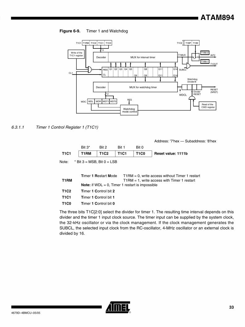
Figure 6-9. Timer 1 and Watchdog
6.3.1.1 Timer 1 Control Register 1 (T1C1)
Note: * Bit 3 = MSB, Bit 0 = LSB
The three bits T1C[2:0] select the divider for timer 1. The resulting time interval depends on this divider and the timer 1 input clock source. The timer input can be supplied by the system clock, the 32-kHz oscillator or via the clock management. If the clock management generates the SUBCL, the selected input clock from the RC-oscillator, 4-MHz oscillator or an external clock is divided by 16.
Q5Q1 Q2 Q3 Q4
Q6
Q8
Q8
Q11
Q11
Q14
Q14
RES
CL
Decoder
Watchdogmode control
MUX for interval timer
Decoder MUX for watchdog timer
T1RM T1C2 T1C1 T1C0
3
2
WDL WDR WDT1 WDT0WDCRES
T1MUX
SUBCL
T1BP T1IM
T1IM=0
T1IM=1
INT2
T1OUT
T1C2
RESET(NRST)
WatchdogDivider/8
DividerRESET
T1C1
Write of theT1C1 register
CL1
WDCL
Read of theCWD register
Address: '7'hex — Subaddress: '8'hex
Bit 3* Bit 2 Bit 1 Bit 0
T1C1 T1RM T1C2 T1C1 T1C0 Reset value: 1111b
T1RMTimer 1 Restart Mode T1RM = 0, write access without Timer 1 restart T1RM = 1, write access with Timer 1 restart Note: if WDL = 0, Timer 1 restart is impossible
T1C2 Timer 1 Control bit 2
T1C1 Timer 1 Control bit 1
T1C0 Timer 1 Control bit 0
334679D–4BMCU–05/05

6.3.1.2 Timer 1 Control Register 2 (T1C2)
Note: 1. Bit 3 = MSB, Bit 0 = LSB
6.3.1.3 Watchdog Control Register (WDC)
Note: 1. Bit 3 = MSB, Bit 0 = LSB
Table 6-6. Timer 1 Control Bits
T1C2 T1C1 T1C0 DividerTime Interval with
SUBCLTime Interval with SUBCL = 32 kHz
Time Interval with SYSCL = 2/1 MHz
0 0 0 2 SUBCL/2 61 µs 1 µs/2 µs
0 0 1 4 SUBCL/4 122 µs 2 µs/4 µs
0 1 0 8 SUBCL/8 244 µs 4 µs/8 µs
0 1 1 16 SUBCL/16 488 µs 8 µs/16 µs
1 0 0 32 SUBCL/32 0.977 ms 16 µs/32 µs
1 0 1 256 SUBCL/256 7.812 ms 128 µs/256 µs
1 1 0 2048 SUBCL/2048 62.5 ms 1024 µs/2048 µs
1 1 1 16384 SUBCL/16384 500 ms 8192 µs/16384 µs
Address: '7'hex — Subaddress: '9'hex
Bit 3(1) Bit 2 Bit 1 Bit 0
T1C2 – T1BP T1CS T1IM Reset value: x111b
T1BPTimer 1 SUBCL ByPassed T1BP = 1, TIOUT = T1MUX T1BP = 0, T1OUT = SUBCL
T1CSTimer 1 input Clock Select T1CS = 1, CL1 = SUBCL (see Figure 6-8 on page 32) T1CS = 0, CL1 = SYSCL (see Figure 6-8 on page 32)
T1IMTimer 1 Interrupt Mask T1IM = 1, disables Timer 1 interrupt T1IM = 0, enables Timer 1 interrupt
Address: '7'hex — Subaddress: 'A'hex
Bit 3(1) Bit 2 Bit 1 Bit 0
WDC WDL WDR WDT1 WDT0 Reset value: 1111b
WDL
WatchDog Lock mode WDL = 1, the watchdog can be enabled and disabled by using the WDR bit WDL = 0, the watchdog is enabled and locked. In this mode the WDR bit has no effect. After the WDL bit is cleared, the watchdog is active until a system reset or power-on reset occurs
WDRWatchDog Run and stop mode WDR = 1, the watchdog is stopped/disabled WDR = 0, the watchdog is active/enabled
WDT1 WatchDog Time 1
WDT0 WatchDog Time 0
344679D–4BMCU–05/05
ATAM894

ATAM894
Both these bits control the time interval for the watchdog reset.
6.3.2 Timer 2
6.3.2.1 Features8/12-bit timer for
• Interrupt, square-wave, pulse and duty cycle generation
• Baud-rate generation for the internal shift register
• Manchester and Bi-phase modulation together with the SSI
• Carrier frequency generation and modulation together with the SSI
Timer 2 can be used as interval timer for interrupt generation, as signal generator or as baud-rate generator and modulator for the serial interface. It consists of a 4-bit and an 8-bit up counter stage which both have compare registers. The 4-bit counter stages of Timer 2 are cas-cadable as an 12-bit timer or as an 8-bit timer with a 4-bit prescaler. The timer can also be configured as an 8-bit timer and separate a 4-bit prescaler.
The Timer 2 input can be supplied via the system clock, the external input clock (T2I), the Timer 1 output clock or the shift clock of the serial interface. The external input clock T2I is not syn-chronized with SYSCL. Therefore, it is possible to use Timer 2 with a higher clock speed than SYSCL. Furthermore, with that input clock the Timer 2 operates in the power-down mode SLEEP (CPU core → sleep and OSC-Stop → yes) as well as in POWER-DOWN (CPU core →sleep and OSC-Stop → no). All other clock sources supply no clock signal in SLEEP if NSTOP = 0. The 4-bit counter stages of Timer 2 have an additional clock output (POUT).
Its output has a modulator stage that allows the generation of pulses as well as the generation and modulation of carrier frequencies. The Timer 2 output can modulate with the shift register data output to generate Bi-phase- or Manchester code.
If the serial interface is used to modulate a bit-stream, the 4-bit stage of Timer 2 has a special task. The shift register can only handle bit-stream lengths divisible by 8. For other lengths, the 4-bit counter stage can be used to stop the modulator after the right bit-count is shifted out.
If the timer is used for carrier frequency modulation, the 4-bit stage works together with an addi-tional 2-bit duty cycle generator like a 6-bit prescaler to generate carrier frequency and duty cycle. The 8-bit counter is used to enable and disable the modulator output for a programmable count of pulses.
Table 6-7. Watchdog Time Control Bits
WDT1 WDT0 DividerDelay Time to Reset with
tin = 1/32 kHzDelay Time to Reset with
tin = 1/(2/1 MHz)
0 0 512 15.625 ms 0.256 ms/0.512 ms
0 1 2048 62.5 ms 1.024 ms/2.048 ms
1 0 16384 0.5 s 8.2 ms/16.4 ms
1 1 131072 4 s 65.5 ms/131 ms
354679D–4BMCU–05/05
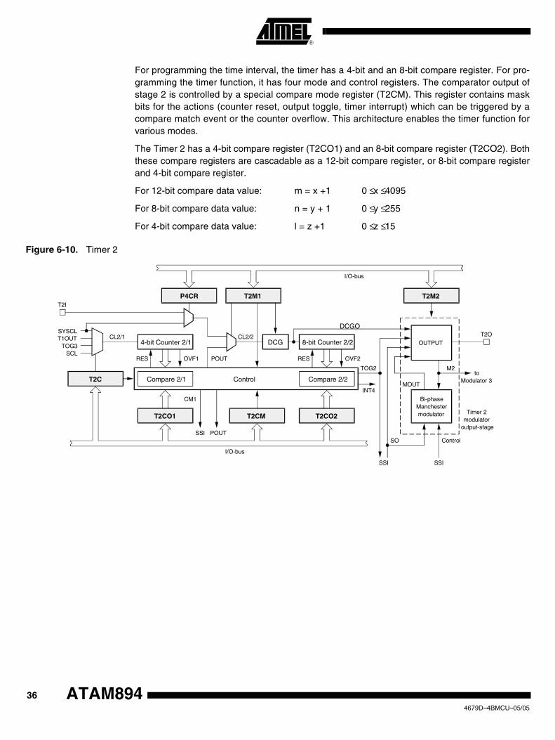
For programming the time interval, the timer has a 4-bit and an 8-bit compare register. For pro-gramming the timer function, it has four mode and control registers. The comparator output of stage 2 is controlled by a special compare mode register (T2CM). This register contains mask bits for the actions (counter reset, output toggle, timer interrupt) which can be triggered by a compare match event or the counter overflow. This architecture enables the timer function for various modes.
The Timer 2 has a 4-bit compare register (T2CO1) and an 8-bit compare register (T2CO2). Both these compare registers are cascadable as a 12-bit compare register, or 8-bit compare register and 4-bit compare register.
For 12-bit compare data value: m = x +1 0 ≤ x ≤ 4095
For 8-bit compare data value: n = y + 1 0 ≤ y ≤ 255
For 4-bit compare data value: l = z +1 0 ≤ z ≤ 15
Figure 6-10. Timer 2
4-bit Counter 2/1
RES OVF1
Compare 2/1
T2CO1
CM1
POUT
SSI POUT
CL2/2DCG
T2M1P4CR
8-bit Counter 2/2
RES OVF2
Compare 2/2
T2CO2T2CM
Control
TOG2
INT4
Bi-phaseManchestermodulator
OUTPUT
MOUT
M2to
Modulator 3
T2O
Timer 2modulator
output-stage
T2M2
SO Control
SSI SSI
I/O-bus
T2C
CL2/1
T2I
SYSCLT1OUT
TOG3SCL
I/O-bus
DCGO
364679D–4BMCU–05/05
ATAM894

ATAM894
6.3.2.2 Timer 2 ModesMode 1: 12-bit Compare Counter
The 4-bit stage and the 8-bit stage work together as a 12-bit compare counter. A compare match signal of the 4-bit and the 8-bit stage generates the signal for the counter reset, toggle flip-flop or interrupt. The compare action is programmable via the compare mode register (T2CM). The 4-bit counter overflow (OVF1) supplies the clock output (POUT) with clocks. The duty cycle gen-erator (DCG) has to be bypassed in this mode.
Figure 6-11. 12-bit Compare Counter
Mode 2: 8-bit Compare Counter with 4-bit Programmable Prescaler
The 4-bit stage is used as a programmable prescaler for the 8-bit counter stage. In this mode, a duty cycle stage is also available. This stage can be used as an additional 2-bit prescaler or for generating duty cycles of 25%, 33% and 50%. The 4-bit compare output (CM1) supplies the clock output (POUT) with clocks.
Figure 6-12. 8-bit Compare Counter
4-bit counter
4-bit compare
RES
4-bit register
CM1
POUT (CL2/1 /16)
8-bit counter
8-bit compare
8-bit register
OVF2
CM2
RES
T2RM T2OTM
Timer 2output mode
and T2OTM-bit
T2IM T2CTM
TOG2
INT4
CL2/1DCG
T2D1, 0
4-bit counter
4-bit compare
RES
4-bit register
CM1
POUT
8-bit counter
8-bit compare
8-bit register
OVF2
CM2
RES
T2RM T2OTM
Timer 2output mode
and T2OTM-bit
T2IM T2CTM
TOG2
INT4
CL2/1DCG
T2D1, 0
DCGO
374679D–4BMCU–05/05

Mode 3/4: 8-bit Compare Counter and 4-bit Programmable Prescaler
In these modes the 4-bit and the 8-bit counter stages work independently as a 4-bit prescaler and an 8-bit timer with an 2-bit prescaler or as a duty cycle generator. Only in the mode 3 and mode 4, can the 8-bit counter be supplied via the external clock input (T2I) which is selected via the P4CR register. The 4-bit prescaler is started via activating of mode 3 and stopped and reset in mode 4. Changing mode 3 and 4 has no effect for the 8-bit timer stage. The 4-bit stage can be used as prescaler for Timer 3, the SSI or to generate the stop signal for modulator 2 and modulator 3.
Figure 6-13. 4-/8-bit Compare Counter
4-bit counter
4-bit compare
RES
4-bit register
8-bit counter
8-bit compare
8-bit register
OVF2
CM2
RES
T2RM T2OTM
Timer 2output mode
and T2OTM-bit
T2IM T2CTM
TOG2
INT4
CL2/2DCG
T2D1, 0
DCGO
P41M2, 1P4CR
CM1 POUT
CL2/1MUX
TOG3T1OUT
SYSCLSCL
T2CS1, 0
SYSCL
T2I
384679D–4BMCU–05/05
ATAM894

ATAM894
6.3.2.3 Timer 2 Output ModesThe signal at the timer output is generated via modulator 2. In the toggle mode, the compare match event toggles the output T2O. For high resolution duty cycle modulation 8 bits or 12 bits can be used to toggle the output. In the duty-cycle burst modulator modes the DCG output is connected to T2O and switched on and off either by the toggle flip-flop output or the serial data line of the SSI. Modulator 2 also has 2 modes to output the content of the serial interface as Bi-phase or Manchester code.
The modulator output stage can be configured by the output control bits in the T2M2 register. The modulator is started with the start of the shift register (SIR = 0) and stopped either by carry-ing out a shift register stop (SIR = 1) or compare match event of stage 1 (CM1) of Timer 2. For this task, Timer 2 mode 3 must be used and the prescaler has to be supplied with the internal shift clock (SCL).
Figure 6-14. Timer 2 Modulator Output Stage
6.3.2.4 Timer 2 Output SignalsTimer 2 Output Mode 1
Toggle Mode A: A Timer 2 compare match toggles the output flip-flop (M2) → T2O
Figure 6-15. Interrupt Timer/Square Wave Generator — the Output Toggles with Each Edge Compare Match Event
Toggle
RES/SET
Bi-phase/Manchestermodulator
T2TOPT2OS2, 1, 0T2M2
T2O
M2
M2
S1S2
S3
Modulator 3
RE
FE
OMSK
SSICONTROL
TOG2
SO
DCGO
40 0 0 1 2 3 40 1 2 3 40 1 2 3 0 1
InputCounter 2
T2R
Counter 2
CMx
INT4
T2O
394679D–4BMCU–05/05

Toggle Mode B: A Timer 2 compare match toggles the output flip-flop (M2) → T2O
Figure 6-16. Pulse Generator — the Timer Output Toggles with the Timer Start if the T2TS bit is Set
Toggle Mode C: A Timer 2 compare match toggles the output flip-flop (M2) → T2O
Figure 6-17. Pulse Generator — the Timer Toggles with Timer Overflow and Compare Match
40 0 0 1 2 3 5 6 7 40 1 2 3 5 6
InputCounter 2
T2R
Counter 2
CMx
INT4
T2OToggleby start
T2O
4095/255
40 0 0 1 2 3 5 6 7 40 1 2 3 5 6
InputCounter 2
T2R
Counter 2
CMx
OVF2
INT4
T2O
4095/255
404679D–4BMCU–05/05
ATAM894

ATAM894
Timer 2 Output Mode 2
Duty Cycle Burst Generator 1: The DCG output signal (DCGO) is given to the output, and
gated by the output flip-flop (M2)
Figure 6-18. Carrier Frequency Burst Modulation with Timer 2 Toggle Flip-flop Output
Timer 2 Output Mode 3
Duty Cycle Burst Generator 2: The DCG output signal (DCGO) is given to the output, and
gated by the SSI internal data output (SO)
Figure 6-19. Carrier Frequency Burst Modulation with the SSI Data Output
Timer 2 Output Mode 4
Bi-phase Modulator: Timer 2 Modulates the SSI Internal Data Output (SO) to Bi-phase Code.
Figure 6-20. Bi-phase Modulation
1 2 0 1 2 0 1 2 3 4 5 0 1 2 0 1 2 3 4 5 6 7 8 0 1 2 3 4 5 6 7 8 9 10 0 1 2 3 4 5
DCGO
Counter 2
TOG2
M2
T2O
Counter = compare register (= 2)
1 2 0 1 2 0 1 2 0 1 2 0 1 2 0 1 2 0 1 2 0 1 2 0 1 2 0 1 2 0 1 2 0 1 2 0 1 2 0 1
DCGO
Counter 2
TOG2
SO
T2O
Counter = compare register (= 2)
Bit 0 Bit 1 Bit 2 Bit 3 Bit 4 Bit 5 Bit 6 Bit 7 Bit 8 Bit 9 Bit 10 Bit 11 Bit 12 Bit 13
TOG2
SC
SO
T2O0 0 00
0 0 1 1 0 1 0 1
1 1 1 1
8-bit SR data
Bit 7 Bit 0
Data: 00110101
414679D–4BMCU–05/05

Timer 2 Output Mode 5
Manchester Modulator: Timer 2 Modulates the SSI internal data output (SO) to Manchester code
Figure 6-21. Manchester Modulation
Timer 2 Output Mode 7
PWM Mode: Pulse-width modulation output on Timer 2 output pin (T2O)
In this mode the timer overflow defines the period and the compare register defines the duty-cycle. During one period only the first compare match occurrence is used to toggle the timer output flip-flop. Until the overflow all further compare match are ignored. This avoids the situation that changing the compare register causes the occurrence of several compare match during one period. The resolution at the pulse-width modulation Timer 2 mode 1 is 12-bit and all other Timer 2 modes are 8-bit.
Figure 6-22. PWM Modulation
TOG2
SC
SO
T2O0 00
0 0 1 1 0 1 0 1
1 1 1 1
8-bit SR data
Bit 7 Bit 0
0
Bit 7 Bit 0
Data: 00110101
0 0 50 255 1000 255 0 150 255 0 50 255 0 100
T2R
Input clockCounter 2/2
Counter 2/2
OVF2
CM2
INT4
T2O
load the nextcompare value T2CO2 = 150 load load
T1 T2 T3 T1 T2T T T T T
424679D–4BMCU–05/05
ATAM894
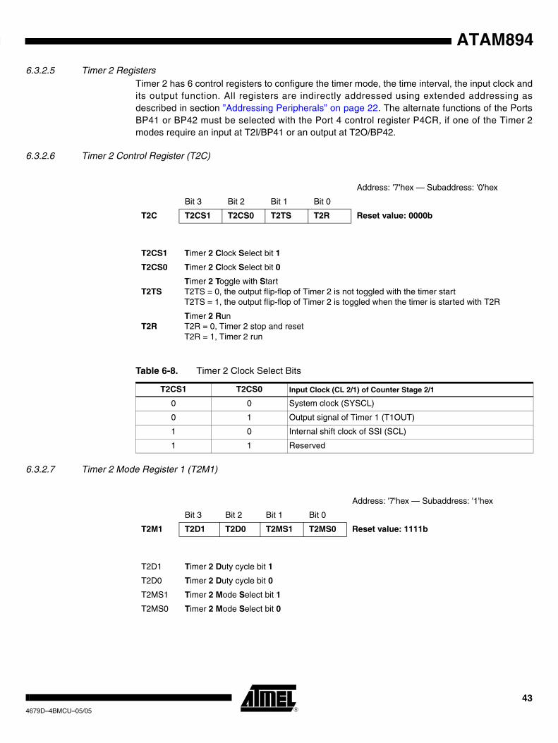
ATAM894
6.3.2.5 Timer 2 RegistersTimer 2 has 6 control registers to configure the timer mode, the time interval, the input clock and its output function. All registers are indirectly addressed using extended addressing as described in section ”Addressing Peripherals” on page 22. The alternate functions of the Ports BP41 or BP42 must be selected with the Port 4 control register P4CR, if one of the Timer 2 modes require an input at T2I/BP41 or an output at T2O/BP42.
6.3.2.6 Timer 2 Control Register (T2C)
6.3.2.7 Timer 2 Mode Register 1 (T2M1)
Address: '7'hex — Subaddress: '0'hex
Bit 3 Bit 2 Bit 1 Bit 0
T2C T2CS1 T2CS0 T2TS T2R Reset value: 0000b
T2CS1 Timer 2 Clock Select bit 1
T2CS0 Timer 2 Clock Select bit 0
T2TSTimer 2 Toggle with Start T2TS = 0, the output flip-flop of Timer 2 is not toggled with the timer start T2TS = 1, the output flip-flop of Timer 2 is toggled when the timer is started with T2R
T2RTimer 2 Run T2R = 0, Timer 2 stop and reset T2R = 1, Timer 2 run
Table 6-8. Timer 2 Clock Select Bits
T2CS1 T2CS0 Input Clock (CL 2/1) of Counter Stage 2/1
0 0 System clock (SYSCL)
0 1 Output signal of Timer 1 (T1OUT)
1 0 Internal shift clock of SSI (SCL)
1 1 Reserved
Address: '7'hex — Subaddress: '1'hex
Bit 3 Bit 2 Bit 1 Bit 0
T2M1 T2D1 T2D0 T2MS1 T2MS0 Reset value: 1111b
T2D1 Timer 2 Duty cycle bit 1
T2D0 Timer 2 Duty cycle bit 0
T2MS1 Timer 2 Mode Select bit 1
T2MS0 Timer 2 Mode Select bit 0
434679D–4BMCU–05/05

6.3.2.8 Duty Cycle GeneratorThe duty cycle generator generates duty cycles of 25%, 33% or 50%. The frequency at the duty cycle generator output depends on the duty cycle and the Timer 2 prescaler setting. The DCG-stage can also be used as an additional programmable prescaler for Timer 2.
Figure 6-23. DCG Output Signals
Table 6-9. Timer 2 Duty Cycle Bits
T2D1 T2D0 Function of Duty Cycle Generator (DCG) Additional Divider Effect
1 1 Bypassed (DCGO0) /1
1 0 Duty cycle 1/1 (DCGO1) /2
0 1 Duty cycle 1/2 (DCGO2) /3
0 0 Duty cycle 1/3 (DCG03) /4
Table 6-10. Timer 2 Mode Select Bits
Mode T2MS1 T2MS0 Clock Output (POUT) Timer 2 Modes
1 1 1 4-bit counter overflow (OVF1)12-bit compare counter, the DCG have to be bypassed in this mode
2 1 0 4-bit compare output (CM1)8-bit compare counter with 4-bit programmable prescaler and duty cycle generator
3 0 1 4-bit compare output (CM1)
8-bit compare counter clocked by SYSCL or the external clock input T2I, 4-bit prescaler run, the counter 2/1 starts after writing mode 3
4 0 0 4-bit compare output (CM1)
8-bit compare counter clocked by SYSCL or the external clock input T2I, 4-bit prescaler stop and resets
DCGIN
DCGO0
DCGO1
DCGO2
DCGO3
444679D–4BMCU–05/05
ATAM894

ATAM894
6.3.2.9 Timer 2 Mode Register 2 (T2M2)
If one of these output modes is used the T2O alternate function of Port 4 must also be activated.
6.3.2.10 Timer 2 Compare and Compare Mode RegistersTimer 2 has two separate compare registers, T2CO1 for the 4-bit stage and T2CO2 for the 8-bit stage of Timer 2. The timer compares the contents of the compare register current counter value and if it matches it generates an output signal. Depending on the timer mode, this signal is used to generate a timer interrupt, to toggle the output flip-flop as SSI clock or as a clock for the next counter stage.
In the 12-bit timer mode, T2CO1 contains bits 0 to 3 and T2CO2 bits 4 to 11 of the 12-bit com-pare value. In all other modes, the two compare registers work independently as a 4- and 8-bit compare register. When assigned to the compare register a compare event will be suppressed.
Address: '7'hex — Subaddress: '2'hex
Bit 3 Bit 2 Bit 1 Bit 0
T2M2 T2TOP T2OS2 T2OS1 T2OS0 Reset value: 1111b
T2TOP
Timer 2 Toggle Output Preset This bit allows the programmer to preset the Timer 2 output T2O. T2TOP = 0, resets the toggle outputs with the write cycle (M2 = 0) T2TOP = 1, sets toggle outputs with the write cycle (M2 = 1) Note: If T2R = 1, no output preset is possible
T2OS2 Timer 2 Output Select bit 2
T2OS1 Timer 2 Output Select bit 1
T2OS0 Timer 2 Output Select bit 0
Table 6-11. Timer 2 Output Select Bits
Output Mode T2OS2 T2OS1 T2OS0 Clock Output
1 1 1 1Toggle mode: a Timer 2 compare match toggles the output flip-flop (M2) → T2O
2 1 1 0Duty cycle burst generator 1: the DCG output signal (DCG0) is given to the output and gated by the output flip-flop (M2)
3 1 0 1Duty cycle burst generator 2: the DCG output signal (DCGO) is given to the output and gated by the SSI internal data output (SO)
4 1 0 0Bi-phase modulator: Timer 2 modulates the SSI internal data output (SO) to Bi-phase code
5 0 1 1Manchester modulator: Timer 2 modulates the SSI internal data output (SO) to Manchester code
6 0 1 0SSI output: T2O is used directly as SSI internal data output (SO)
7 0 0 1 PWM mode: an 8/12-bit PWM mode
8 0 0 0 Not allowed
454679D–4BMCU–05/05

6.3.2.11 Timer 2 Compare Mode Register (T2CM)
6.3.2.12 Timer 2 COmpare Register 1 (T2CO1)
In prescaler mode the clock is bypassed if the compare register T2CO1 contains 0.
6.3.2.13 Timer 2 COmpare Register 2 (T2CO2) Byte Write
Address: '7'hex — Subaddress: '3'hex
Bit 3 Bit 2 Bit 1 Bit 0
T2CM T2OTM T2CTM T2RM T2IM Reset value: 0000b
T2OTM
Timer 2 Overflow Toggle Mask bit T2OTM = 0, disable overflow toggle T2OTM = 1, enable overflow toggle, a counter overflow (OVF2) toggles output flip-flop (TOG2). If the T2OTM bit is set, only a counter overflow can generate an interrupt except on the Timer 2 output mode 7
T2CTM
Timer 2 Compare Toggle Mask bit T2CTM = 0, disable compare toggle T2CTM = 1, enable compare toggle, a match of the counter with the compare register toggles output flip-flop (TOG2). In Timer 2 output mode 7 and when the T2CTM bit is set, only a match of the counter with the compare register can generate an interrupt
T2RM
Timer 2 Reset Mask bit T2RM = 0, disable counter reset T2RM = 1, enable counter reset, a match of the counter with the compare register resets the counter
T2IMTimer 2 Interrupt Mask bit T2IM = 0, disable Timer 2 interrupt T2IM = 1, enable Timer 2 interrupt
Table 6-12. Timer 2 Toggle Mask Bits
Timer 2 Output Mode T2OTM T2CTM Timer 2 Interrupt Source
1, 2, 3, 4, 5 and 6 0 x Compare match (CM2)
1, 2, 3, 4, 5 and 6 1 x Overflow (OVF2)
7 x 1 Compare match (CM2)
Address: '7'hex — Subaddress: '4'hex
T2CO1 Write cycle Bit 3 Bit 2 Bit 1 Bit 0 Reset value: 1111b
Address: '7’hex — Subaddress: '5'hex
T2CO2 First write cycle Bit 3 Bit 2 Bit 1 Bit 0 Reset value: 1111b
Second write cycle
Bit 7 Bit 6 Bit 5 Bit 4 Reset value: 1111b
464679D–4BMCU–05/05
ATAM894

ATAM894
6.3.3 Timer 3
6.3.3.1 Features
• Two Compare Registers
• Capture Register
• Edge Sensitive Input with Zero Cross Detection Capability
• Trigger and Single Action Modes
• Output Control Modes
• Automatic Modulation and Demodulation Modes
• FSK Modulation
• Pulse width Modulation (PWM)
• Manchester Demodulation Together with SSI
• Bi-phase Demodulation Together with SSI
• Pulse-width Demodulation Together with SSI
Figure 6-24. Timer 3
Timer 3 consists of an 8-bit up-counter with two compare registers and one capture register. The timer can be used as event counter, timer and signal generator. Its output can be programmed as modulator and demodulator for the serial interface. The two compare registers enable various modes of signal generation, modulation and demodulation. The counter can be driven by inter-nal and external clock sources. For external clock sources, it has a programmable edge-sensitive input which can be used as counter input, capture signal input or trigger input. This timer input is synchronized with SYSCL. Therefore, in the power-down mode SLEEP (CPU core → sleep and OSC-Stop → yes), this timer input is stopped too. The counter is readable via its capture register while it is running. In capture mode, the counter value can be captured by a pro-grammable capture event from the Timer 3 input or Timer 2 output.
8-bit Counter 3
RES
Compare 3/1
T3CO1
T3CP
T3CO2
Control
T3O
CL3
T3I
T3EXSYSCLT1OUT
POUT
I/O-bus
Compare 3/2
T3CM1 T3CM2
T3C T3ST
Modulator 3
Demodu-lator 3
M2ControlSO
TOG3
INT5
RES
CM31
T3I
T3EX
TOG2
SI
SCI
T3MT3CS
I/O-bus
Timer 2 SSI SSI
CP3
474679D–4BMCU–05/05

A special feature of this timer is the trigger- and single-action mode. In trigger mode, the counter starts counting triggered by the external signal at its input. In single-action mode, the counter counts only one time up to the programmed compare match event. These modes are very useful for modulation, demodulation, signal generation, signal measurement and phase control. For phase control, the timer input is protected against negative voltages and has zero-cross detec-tion capability.
Timer 3 has a modulator output stage and input functions for demodulation. As modulator it works together with Timer 2 or the serial interface. When the shift register is used for modulation the data shifted out of the register is encoded bit-wise. In all demodulation modes, the decoded data bits are shifted automatically into the shift register.
Figure 6-25. Counter 3 Stage
6.3.3.2 Timer/Counter ModesTimer 3 has 6 timer modes and 6 modulator/demodulator modes. The mode is set via the Timer 3 Mode Register T3M.
In all these modes, the compare register and the compare-mode register belonging to it define the counter value for a compare match and the action of a compare match. A match of the cur-rent counter value with the content of one compare register triggers a counter reset, a Timer 3 interrupt or the toggling of the output flip-flop. The compare mode registers T3M1 and T3M2 contain the mask bits for enabling or disabling these actions.
The counter can also be enabled to execute single actions with one or both compare registers. If this mode is set the corresponding compare match event is generated only once after the counter starts.
8-bit comparator
Compare register 1
RES
Capture register
8-bit counter
Compare register 2
ControlC31
C32
Control
T3SM1NQ
D T3RM1 T3IM1 T3TM1
TOG2 T3I
T3TM2T3IM2T3RM2T3SM2NQ
D
CL3
T3EIM
TOG3
INT5
CM31
CM32
: T3M1
: T3M2
484679D–4BMCU–05/05
ATAM894
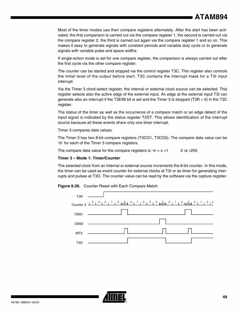
ATAM894
Most of the timer modes use their compare registers alternately. After the start has been acti-vated, the first comparison is carried out via the compare register 1, the second is carried out via the compare register 2, the third is carried out again via the compare register 1 and so on. This makes it easy to generate signals with constant periods and variable duty cycle or to generate signals with variable pulse and space widths.
If single-action mode is set for one compare register, the comparison is always carried out after the first cycle via the other compare register.
The counter can be started and stopped via the control register T3C. This register also controls the initial level of the output before start. T3C contains the interrupt mask for a T3I input interrupt.
Via the Timer 3 clock-select register, the internal or external clock source can be selected. This register selects also the active edge of the external input. An edge at the external input T3I can generate also an interrupt if the T3EIM bit is set and the Timer 3 is stopped (T3R = 0) in the T3C register.
The status of the timer as well as the occurrence of a compare match or an edge detect of the input signal is indicated by the status register T2ST. This allows identification of the interrupt source because all these events share only one timer interrupt.
Timer 3 compares data values.
The Timer 3 has two 8-bit compare registers (T3CO1, T3CO2). The compare data value can be ‘m’ for each of the Timer 3 compare registers.
The compare data value for the compare registers is: m = x +1 0 ≤ x ≤ 255
Timer 3 – Mode 1: Timer/Counter
The selected clock from an internal or external source increments the 8-bit counter. In this mode, the timer can be used as event counter for external clocks at T3I or as timer for generating inter-rupts and pulses at T3O. The counter value can be read by the software via the capture register.
Figure 6-26. Counter Reset with Each Compare Match
00 0 0 1 2 3 51 2 3 4 00 1 2 3 1 2
T3R
Counter 3
CM31
INT5
T3O
3
CM32
494679D–4BMCU–05/05

Figure 6-27. Counter Reset with Compare Register 2 and Toggle with Start
Figure 6-28. Single Action of Compare Register 1
Timer 3 – Mode 2: Timer/Counter, External Trigger Restart and External Capture (with T3I Input)
The counter is driven by an internal clock source. After starting with T3R, the first edge from the external input T3I starts the counter. The following edges at T3I load the current counter value into the capture register, resets the counter and restarts it. The edge can be selected by the pro-grammable edge decoder of the timer input stage. If single-action mode is activated for one or both compare registers the trigger signal restarts the single action.
Figure 6-29. Externally Triggered Counter Reset and Start Combined with Single-action Mode
40 0 0 1 2 3 5 6 7 40 1 2 3 5 6
T3R
Counter 3
CM31
INT5
T3O
Toggleby start
T3O
8 9
CL3
CM32
0 0 1 2 3 4 5 6 7 8 9 10 0 1 2Counter 3
CM31
CM32
T3O
0 1 2 0 1 2 0 1 2 0 1 2 0 1 2 0 1 2 0 1 2 0 1 2 0 1
Toggle by start
T3R
0 0 0 0 0 0 0 0 1 2 3 4 5 6Counter 3
T3EX
CM31
CM32
7 8 9 10 0 1 2 X X X 0 1 2 3 4 5 6 7 8 9 10 0 1 2 X X
T3R
X X
T3O
504679D–4BMCU–05/05
ATAM894

ATAM894
Timer 3 – Mode 3: Timer/Counter, Internal Trigger Restart and Internal Capture (with TOG2)
The counter is driven by an internal or external (T3I) clock source. The output toggle signal of Timer 2 resets the counter. The counter value before the reset is saved in the capture register. If single-action mode is activated for one or both compare registers, the trigger signal restarts the single actions. This mode can be used for frequency measurements or as event counter with time gate (see section “Combination Mode 10”).
Figure 6-30. Event Counter with Time Gate
Timer 3 - Mode 4: Timer/Counter
The timer runs as timer/counter in mode 1, but its output T3O is used as output for the Timer 2 output signal.
Timer 3 – Mode 5: Timer/Counter, External Trigger Restart and External Capture (with T3I Input)
The Timer 3 runs as timer/counter in mode 2, but its output T3O is used as output for the Timer 2 output signal.
6.3.3.3 Timer 3 Modulator/Demodulator ModesTimer 3 – Mode 6: Carrier Frequency Burst Modulation Controlled by Timer 2 Output
Toggle Flip-Flop (M2)
The Timer 3 counter is driven by an internal or external clock source. Its compare- and compare mode registers must be programmed to generate the carrier frequency via the output toggle flip-flop. The output toggle flip-flop of Timer 2 is used to enable or disable the Timer 3 output. Timer 2 can be driven by the toggle output signal of Timer 3 or any other clock source (see sec-tion “Combination Mode 11”).
Timer 3 – Mode 7: Carrier Frequency Burst Modulation Controlled by SSI Internal Output (SO)
The Timer 3 counter is driven by an internal or external clock source. Its compare- and compare mode registers must be programmed to generate the carrier frequency via the output toggle flip-flop. The output (SO) of the SSI is used to enable or disable the Timer 3 output. The SSI should be supplied with the toggle signal of Timer 2 (see section “Combination Mode 12”).
0 0 1 2 3 4 5 6 7 8 910Counter 3
TOG2T3CP-Register
11 0 1 2 4 0 1
T3I
23
T3R
Capture value = 0 Capture value = 11 Capturevalue = 4
514679D–4BMCU–05/05

Timer 3 – Mode 8: FSK Modulation with Shift Register Data (SO)
The two compare registers are used for generating two different time intervals. The SSI internal data output (SO) selects which compare register is used for the output frequency generation. A '0' level at the SSI data output enables the compare register 1. A '1' level enables compare reg-ister 2. The compare- and compare mode registers must be programmed to generate the two frequencies via the output toggle flip-flop. The SSI can be supplied with the toggle signal of Timer 2. The Timer 3 counter is driven by an internal or external clock source. The Timer 2 counter is driven by the Counter 3 (TOG3) (see section “Combination Mode 13”).
Figure 6-31. FSK Modulation
Timer 3 – Mode 9: Pulse-width Modulation with the Shift Register
The two compare registers are used for generating two different time intervals. The SSI internal data output (SO) selects which compare register is used for the output pulse generation. In this mode both compare- and compare mode registers must be programmed for generating the two pulse widths. It is also useful to enable the single-action mode for extreme duty-cycles. Timer 2 is used as baud-rate generator and for the trigger restart of Timer 3. The SSI must be supplied with a toggle signal of Timer 2. The counter is driven by an internal or external clock source (see section “Combination Mode 7”).
Figure 6-32. Pulse-width Modulation
0 1 2 3 4 0 1 2 3 4 0 1 2 3Counter 3
CM31
CM32
SO
4 0 1 2 0 1 2 0 1 2 0 1 2 0 1 2 0 1 2 0 1 2 0 1 2 3
T3R
4 0
T3O
1
0 1 0
0 0 0 0 0 0 0 0 0 0 0 0 0Counter 3
CM31
CM32
T3O
0 0 0 0 0 1 2 3 4 5 6 7 8 9101112131415 0 1 2 3 4 5
TOG2
6 7 8
1
9 111210 1413 0 2 31 4150
00 1
SIR
SO
SCO
T3R
524679D–4BMCU–05/05
ATAM894

ATAM894
Timer 3 – Mode 10: Manchester Demodulation/ Pulse-width Demodulation
For Manchester demodulation, the edge detection stage must be programmed to detect each edge at the input. These edges are evaluated by the demodulator stage. The timer stage is used to generate the shift clock for the SSI. The compare register 1 match event defines the correct moment for shifting the state from the input T3I as the decoded bit into shift register - after that the demodulator waits for the next edge to synchronize the timer by a reset for the next bit. The compare register 2 can also be used to detect a time-out error and handle it with an interrupt routine (see section “Combination Mode 8”).
Figure 6-33. Manchester Demodulation
Timer 3 – Mode 11: Bi-phase Demodulation
In the Bi-phase demodulation mode, the timer operates like in Manchester demodulation mode. The difference is that the bits are decoded via a toggle flip-flop. This flip-flop samples the edge in the middle of the bit-frame and the compare register 1 match event shifts the toggle flip-flop out-put into a shift register (see section “Combination Mode 9”).
Figure 6-34. Bi-phase Demodulation
1 0 1 1 1 0 0 1 1 0
1 1
BIT 0 BIT 1 BIT 2 BIT 3 BIT 4 BIT 5 BIT 6
Synchronize Manchester demodulation modeTimer 3mode
T3EX
SI
SR-DATA
T3I
CM31 = SCI
1 0 0 1 1 0
0 1 1 1 1
0 1
Bit 7 Bit 6 Bit 5 Bit 4 Bit 3 Bit 2 Bit 1
Synchronize Bi-phase demodulation modeTimer 3mode
T3EX
Q1 = SI
CM31 = SCI
SR-DATA
0 0 0 0T3I
ResetCounter 3
1 0 1 0 1 0
Bit 0
534679D–4BMCU–05/05

Timer 3 – Mode 12: Timer/Counter with External Capture Mode (T3I)
The counter is driven by an internal clock source and an edge at the external input T3I loads the counter value into the capture register. The edge can be selected with the programmable edge detector of the timer input stage. This mode can be used for signal and pulse measurements.
Figure 6-35. External Capture Mode
6.3.3.4 Timer 3 Modulator for Carrier Frequency Burst ModulationIf the output stage operates as pulse-width modulator for the shift register the output can be stopped with stage 1 of Timer 2. For this task, the timer mode 3 must be used and the prescaler must be supplied by the internal shift clock of the shift register.
The modulator can be started with the start of the shift register (SIR = 0) and stopped either by a shift register stop (SIR = 1) or compare match event of stage 1 of Timer 2. For this task, the Timer 2 must be used in mode 3 and the prescaler stage must be supplied by the internal shift clock of the shift register.
Figure 6-36. Modulator 3
0 1 2 3 4 5 6 7 8 9 1011Counter 3
T3CP-Register
15
T3I
T3R
Capture value = X Capture value = 17 Capture value = 35
0 121314 16 20171819 2221 23 27242526 2928 30 34313233 3635 37 41383940
T3
Set Res
T3OT3TOP
OMSK
TOG3
SO
SSI/Control
M2
M3
MUX
T3M
0
1
2
3
Timer 3 Mode T3O
6 MUX 17 MUX 29 MUX 3
other MUX 0
544679D–4BMCU–05/05
ATAM894

ATAM894
6.3.3.5 Timer 3 Demodulator for Bi-phase, Manchester and Pulse-width-modulated SignalsThe demodulator stage of Timer 3 can be used to decode Bi-phase, Manchester and puls-width-coded signals
Figure 6-37. Timer 3 Demodulator 3
6.3.3.6 Timer 3 Registers
6.3.3.7 Timer 3 Mode Register (T3M)
Demodulator 3
T3EX Res
CM31 Counter 3Reset
Counter 3Control
SCI
SI
T3I
T3M
Address: 'B'hex — Subaddress: '0'hex
Bit 3 Bit 2 Bit 1 Bit 0
T3M3 T3M2 T3M1 T3M0 Reset value: 1111b
T3M3 Timer 3 Mode select bit 3
T3M2 Timer 3 Mode select bit 2
T3M1 Timer 3 Mode select bit 1
T3M0 Timer 3 Mode select bit 0
Table 6-13. Timer 3 Mode Select Bits
Mode T3M3 T3M2 T3M1 T3M0 Timer 3 Modes
1 1 1 1 1 Timer/counter with a read access
2 1 1 1 0Timer/counter, external capture and external trigger restart mode (T3I)
3 1 1 0 1Timer/counter, internal capture and internal trigger restart mode (TOG2)
4 1 1 0 0 Timer/counter mode 1 without output (T2O -> T3O)
5 1 0 1 1 Timer/counter mode 2 without output (T2O -> T3O)
6 1 0 1 0 Burst modulation with Timer 2 (M2)
7 1 0 0 1 Burst modulation with shift register (SO)
8 1 0 0 0 FSK modulation with shift register (SO)
9 0 1 1 1Pulse-width modulation with shift register (SO) and Timer 2 (TOG2), internal trigger restart (SCO) -> counter reset
554679D–4BMCU–05/05

Note: 1. In this mode, the SSI can be used only as demodulator (8-bit NRZ rising edge). All other SSI modes are not allowed.
6.3.3.8 Timer 3 Control Register 1 (T3C) Write
6.3.3.9 Timer 3 Status Register 1 (T3ST) Read
Note: The status bits T3C1, T3C2 and T3ED will be reset after a READ access to T3ST.
10 0 1 1 0Manchester demodulation/pulse-width demodulation(1) (T2O -> T3O)
11 0 1 0 1 Biphase demodulation (T2O -> T3O)
12 0 1 0 0 Timer/counter with external capture mode (T3I)
13 0 0 1 1 Not allowed
14 0 0 1 0 Not allowed
15 0 0 0 1 Not allowed
16 0 0 0 0 Not allowed
Table 6-13. Timer 3 Mode Select Bits (Continued)
Mode T3M3 T3M2 T3M1 T3M0 Timer 3 Modes
Primary register address: 'C'hex — Write
Bit 3 Bit 2 Bit 1 Bit 0
Write T3EIM T3TOP T3TS T3R Reset value: 0000b
T3EIMTimer 3 Edge Interrupt Mask T3EIM = 0, disables the interrupt when an edge event for Timer 3 occurs (T3I) T3EIM = 1, enables the interrupt when an edge event for Timer 3 occurs (T3I)
T3TOPTimer 3 Toggle Output Preset T3TOP = 0, sets toggle output (M3) to '0'
............. ...... T3TOP = 1, sets toggle output (M3) to '1'
............. ...... Note: If T3R = 1, no output preset is possible
T3TSTimer 3 Toggle with Start . T3TS = 0, Timer 3 output is not toggled during the start
...... ...... T3TS = 1, Timer 3 output is toggled if started with T3R
T3RTimer 3 Run ...... ...... T3R = 0, Timer 3 stop and reset
...... ...... T3R = 1, Timer 3 run
Primary register address: 'C'hex — Read
Bit 3 Bit 2 Bit 1 Bit 0
Read - - - T3ED T3C2 T3C1 Reset value: x000b
T3EDTimer 3 Edge Detect This bit will be set by the edge-detect logic of Timer 3 input (T3I)
T3C2Timer 3 Compare 2 This bit will be set when a match occurs between Counter 3 and T3CO2
T3C1Timer 3 Compare 1 This bit will be set when a match occurs between Counter 3 and T3CO1
564679D–4BMCU–05/05
ATAM894

ATAM894
6.3.3.10 Timer 3 Clock Select Register (T3CS)
6.3.3.11 Timer 3 Compare- and Compare Mode RegisterTimer 3 has two separate compare registers T3CO1 and T3CO2 for the 8-bit stage of Timer 3. The timer compares the content of the compare register with the current counter value. If both match, it generates a signal. This signal can be used for the counter reset, to generate a timer interrupt, for toggling the output flip-flop, as SSI clock or as clock for the next counter stage. For each compare register, a compare-mode register exists. These registers contain mask bits to enable or disable the generation of an interrupt, a counter reset, or an output toggling with the occurrence of a compare match of the corresponding compare register. The mask bits for acti-vating the single-action mode can also be located in the compare mode registers. When assigned to the compare register a compare event will be suppressed.
Address: 'B'hex — Subaddress: '1'hex
Bit 3 Bit 2 Bit 1 Bit 0
T3CS T3E1 T3E0 T3CS1 T3CS0 Reset value: 1111b
T3E1 Timer 3 Edge select bit 1
T3E0 Timer 3 Edge select bit 0
Table 6-14. Timer 3 Edge Select Bits
T3E1 T3E0 Timer 3 Input Edge Select (T3I)
1 1 –
1 0 Positive edge at T3I pin
0 1 Negative edge at T3I pin
0 0 Each edge at T3I pin
T3CS1 Timer 3 Clock Source select bit 1
T3CS0 Timer 3 Clock Source select bit 0
Table 6-15. Timer 3 Clock Select Bits
T3CS1 TCS0 Counter 3 Input Signal (CL3)
1 1 System clock (SYSCL)
1 0 Output signal of Timer 2 (POUT)
0 1 Output signal of Timer 1 (T1OUT)
0 0 External input signal from T3I edge detect
574679D–4BMCU–05/05

6.3.3.12 Timer 3 Compare Mode Register 1 (T3CM1)
T3CM1 contains the mask bits for the match event of the Counter 3 compare register 1
6.3.3.13 Timer 3 Compare Mode Register 2 (T3CM2)
T3CM2 contains the mask bits for the match event of Counter 3 compare register 2
Address: 'B'hex — Subaddress: '2'hex
Bit 3 Bit 2 Bit 1 Bit 0
T3CM1 T3SM1 T3TM1 T3RM1 T3IM1 Reset value: 0000b
T3SM1
Timer 3 Single action Mask bit 1 T3SM1 = 0, disables single-action compare mode T3SM1 = 1, enables single-compare mode. After this bit is set, the compare register (T3CO1) is used until the next compare match
T3TM1
Timer 3 compare Toggle action Mask bit 1 T3TM1 = 0, disables compare toggle T3TM1 = 1, enables compare toggle. A match of Counter 3 with the compare register (T3CO1) toggles the output flip-flop (TOG3)
T3RM1
Timer 3 Reset Mask bit 1 T3RM1 = 0, disables counter reset T3RM1 = 1, enables counter reset. A match of Counter 3 with the compare register (T3CO1) resets the Counter 3
T3IM1Timer 3 Interrupt Mask bit 1 T3RM1 = 0, disables Timer 3 interrupt for T3CO1 register. T3RM1 = 1, enables Timer 3 interrupt for T3CO1 register
Address: 'B'hex — Subaddress: '3'hex
Bit 3 Bit 2 Bit 1 Bit 0
T3CM2 T3SM2 T3TM2 T3RM2 T3IM2 Reset value: 0000b
T3SM2
Timer 3 Single action Mask bit 2 T3SM2 = 0, disables single-action compare mode T3SM2 = 1, enables single-compare mode. After this bit is set, the compare register (T3CO2) is used until the next compare match
T3TM2
Timer 3 compare Toggle action Mask bit 2 T3TM2 = 0, disables compare toggle T3TM2 = 1, enables compare toggle. A match of Counter 3 with the compare register (T3CO2) toggles the output flip-flop (TOG3)
T3RM2
Timer 3 Reset Mask bit 2 T3RM2 = 0, disables counter reset T3RM2 = 1, enables counter reset. A match of Counter 3 with the compare register (T3CO2) resets the Counter 3
T3IM2Timer 3 Interrupt Mask bit 2 T3RM2 = 0, disables Timer 3 interrupt for T3CO2 register T3RM2 = 1, enables Timer 3 interrupt for T3CO2 register
584679D–4BMCU–05/05
ATAM894

ATAM894
The compare registers and corresponding counter reset masks can be used to program the counter time intervals and the toggle masks can be used to program the output signal. The sin-gle-action mask can also be used in this mode. It starts operating after the timer started with T3R.
6.3.3.14 Timer 3 COmpare Register 1 (T3CO1) Byte Write
6.3.3.15 Timer 3 COmpare Register 2 (T3CO2) Byte Write
6.3.3.16 Timer 3 Capture RegisterThe counter content can be read via the capture register. There are two ways to use the capture register. In modes 1 and 4, it is possible to read the current counter value directly out of the cap-ture register. In the capture modes 2, 3, 5 and 12, a capture event like an edge at the Timer 3 input or a signal from Timer 2 stores the current counter value into the capture register. This counter value can be read from the capture register.
6.3.3.17 Timer 3 CaPture Register (T3CP) Byte Read
Address: 'B'hex — Subaddress: '4'hex
High Nibble
Second write cycle Bit 7 Bit 6 Bit 5 Bit 4 Reset value: 1111b
Low Nibble
First write cycle Bit 3 Bit 2 Bit 1 Bit 0 Reset value: 1111b
Address: 'B'hex — Subaddress: '5'hex
High Nibble
Second write cycle Bit 7 Bit 6 Bit 5 Bit 4 Reset value: 1111b
Low Nibble
First write cycle Bit 3 Bit 2 Bit 1 Bit 0 Reset value: 1111b
Address: 'B'hex — Subaddress: ’4'hex
High Nibble
First read cycle Bit 7 Bit 6 Bit 5 Bit 4 Reset value: xxxxb
Low Nibble
Second read cycle Bit 3 Bit 2 Bit 1 Bit 0 Reset value: xxxxb
594679D–4BMCU–05/05

6.3.4 Synchronous Serial Interface (SSI)
6.3.4.1 SSI Features
• 2- and 3-wire NRZ
• 2-wire mode (MCL compatible), additional internal 2-wire link for multi-chip packaging solutions
• With Timer 2
– Bi-phase modulation
– Manchester modulation
– Pulse-width demodulation
– Burst modulation
• With Timer 3
– Pulse-width modulation (PWM)
– FSK modulation
– Bi-phase demodulation
– Manchester demodulation
– Pulse-width demodulation
– Pulse position Demodulation
6.3.4.2 SSI Peripheral ConfigurationThe synchronous serial interface (SSI) can be used either for serial communication with external devices such as EEPROMs, shift registers, display drivers, other microcontrollers, or as a means for generating and capturing on-chip serial streams of data. External data communication takes place via the Port 4 (BP4), a multi-functional port which can be software configured by writing the appropriate control word into the P4CR register. The SSI can be configured in any of the following ways:
1. 2-wire external interface for bi-directional data communication with one data terminal and one shift clock. The SSI uses the Port BP43 as a bi-directional serial data line (SD) and BP40 as shift clock line (SC).
2. 3-wire external interface for simultaneous input and output of serial data, with a serial input data terminal (SI), a serial output data terminal (SO) and a shift clock (SC). The SSI uses BP40 as shift clock (SC), while the serial data input (SI) is applied to BP43 (configured in P4CR as input!). Serial output data (SO) in this case is passed through to BP42 (configured in P4CR to T2O) via the Timer 2 output stage (T2M2 configured in mode 6).
3. Timer/SSI combined modes - the SSI used together with Timer 2 or Timer 3 is capable of performing a variety of data modulation and demodulation functions (see section “Timer”). The modulating data is converted by the SSI into a continuous serial stream of data which is in turn modulated in one of the timer functional blocks. Serial demodu-lated data can be serially captured in the SSI and read by the controller. In the Timer 3 modes 10 and 11 (demodulation modes) the SSI can only be used as demodulator.
4. Multi-chip link (MCL) – the SSI can also be used as an interchip data interface for use in single package multi-chip modules or hybrids. For such applications, the SSI is pro-vided with two dedicated pads (MCL_SD and MCL_SC) which act as a two-wire chip-to-chip link. The MCL can be activated by the MCL control bit. Should these MCL pads be used by the SSI, the standard SD and SC pins are not required and the correspond-ing Port 4 ports are available as conventional data ports.
604679D–4BMCU–05/05
ATAM894

ATAM894
Figure 6-38. Block Diagram of the Synchronous Serial Interface
6.3.4.3 General SSI OperationThe SSI is comprised essentially of an 8-bit shift register with two associated 8-bit buffers the receive buffer (SRB) for capturing the incoming serial data and a transmit buffer (STB) for inter-mediate storage of data to be serially output. Both buffers are directly accessible by software. Transferring the parallel buffer data into and out of the shift register is controlled automatically by the SSI control, so that both single byte transfers or continuous bit streams can be supported.
The SSI can generate the shift clock (SC) either from one of several on-chip clock sources or accept an external clock. The external shift clock is output on, or applied to the Port BP40. Selection of an external clock source is performed by the Serial Clock Direction control bit (SCD). In the combinational modes, the required clock is selected by the corresponding timer mode.
The SSI can operate in three data transfer modes - synchronous 8-bit shift mode, MCL compati-ble 9-bit shift modes or 8-bit pseudo MCL protocol (without acknowledge-bit).
External SSI clocking is not supported in these modes. The SSI should thus generate and has full control over the shift clock so that it can always be regarded as an MCL Bus Master device.
All directional control of the external data port used by the SSI is handled automatically and is dependent on the transmission direction set by the Serial Data Direction (SDD) control bit. This control bit defines whether the SSI is currently operating in Transmit (TX) mode or Receive (RX) mode.
Serial data is organized in 8-bit telegrams which are shifted with the most significant bit first. In the 9-bit MCL mode, an additional acknowledge bit is appended to the end of the telegram for handshaking purposes (see section ”MCL Bus Protocol” on page 65).
At the beginning of every telegram, the SSI control loads the transmit buffer into the shift register and proceeds immediately to shift data serially out. At the same time, incoming data is shifted into the shift register input. This incoming data is automatically loaded into the receive buffer when the complete telegram has been received. Thus, data can be simultaneously received and transmitted if required.
8-bit Shift RegisterMSB LSB
Shift_CL
SO
SIC1 SIC2 SISC
SCControl
STB SRB
SI
Timer 2/Timer 3
Output
INT3
SC
I/O-bus
I/O-bus
SSI-Control
TOG2POUT
T1OUTSYSCL
SO SI
MCL_SC
SD
MCL_SD
TransmitBuffer
ReceiveBuffer
SCI
/2
614679D–4BMCU–05/05
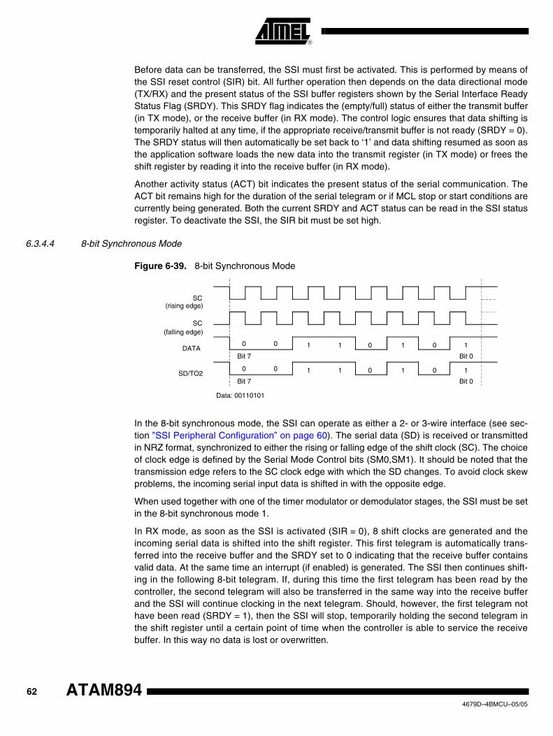
Before data can be transferred, the SSI must first be activated. This is performed by means of the SSI reset control (SIR) bit. All further operation then depends on the data directional mode (TX/RX) and the present status of the SSI buffer registers shown by the Serial Interface Ready Status Flag (SRDY). This SRDY flag indicates the (empty/full) status of either the transmit buffer (in TX mode), or the receive buffer (in RX mode). The control logic ensures that data shifting is temporarily halted at any time, if the appropriate receive/transmit buffer is not ready (SRDY = 0). The SRDY status will then automatically be set back to ‘1’ and data shifting resumed as soon as the application software loads the new data into the transmit register (in TX mode) or frees the shift register by reading it into the receive buffer (in RX mode).
Another activity status (ACT) bit indicates the present status of the serial communication. The ACT bit remains high for the duration of the serial telegram or if MCL stop or start conditions are currently being generated. Both the current SRDY and ACT status can be read in the SSI status register. To deactivate the SSI, the SIR bit must be set high.
6.3.4.4 8-bit Synchronous Mode
Figure 6-39. 8-bit Synchronous Mode
In the 8-bit synchronous mode, the SSI can operate as either a 2- or 3-wire interface (see sec-tion ”SSI Peripheral Configuration” on page 60). The serial data (SD) is received or transmitted in NRZ format, synchronized to either the rising or falling edge of the shift clock (SC). The choice of clock edge is defined by the Serial Mode Control bits (SM0,SM1). It should be noted that the transmission edge refers to the SC clock edge with which the SD changes. To avoid clock skew problems, the incoming serial input data is shifted in with the opposite edge.
When used together with one of the timer modulator or demodulator stages, the SSI must be set in the 8-bit synchronous mode 1.
In RX mode, as soon as the SSI is activated (SIR = 0), 8 shift clocks are generated and the incoming serial data is shifted into the shift register. This first telegram is automatically trans-ferred into the receive buffer and the SRDY set to 0 indicating that the receive buffer contains valid data. At the same time an interrupt (if enabled) is generated. The SSI then continues shift-ing in the following 8-bit telegram. If, during this time the first telegram has been read by the controller, the second telegram will also be transferred in the same way into the receive buffer and the SSI will continue clocking in the next telegram. Should, however, the first telegram not have been read (SRDY = 1), then the SSI will stop, temporarily holding the second telegram in the shift register until a certain point of time when the controller is able to service the receive buffer. In this way no data is lost or overwritten.
SC
SC
DATA
SD/TO2
1 1 0 1 0 10 0
Bit 7 Bit 0
1 1 0 1 0 10 0
Bit 7 Bit 0
Data: 00110101
(rising edge)
(falling edge)
624679D–4BMCU–05/05
ATAM894
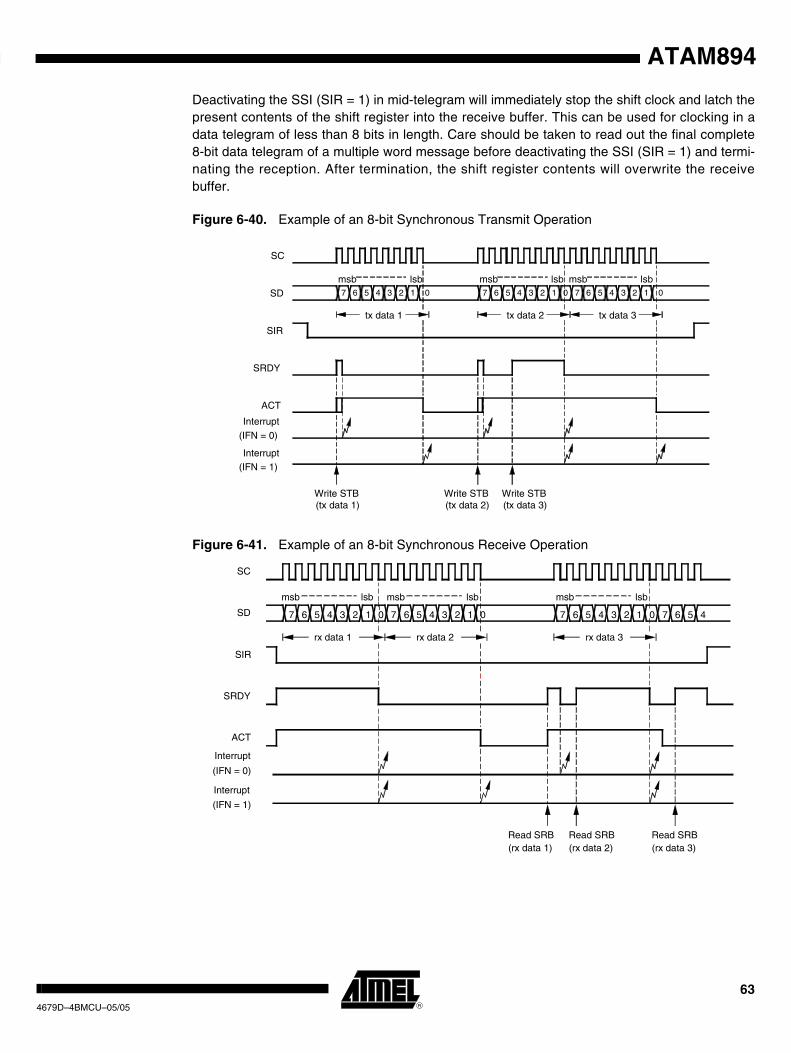
ATAM894
Deactivating the SSI (SIR = 1) in mid-telegram will immediately stop the shift clock and latch the present contents of the shift register into the receive buffer. This can be used for clocking in a data telegram of less than 8 bits in length. Care should be taken to read out the final complete 8-bit data telegram of a multiple word message before deactivating the SSI (SIR = 1) and termi-nating the reception. After termination, the shift register contents will overwrite the receive buffer.
Figure 6-40. Example of an 8-bit Synchronous Transmit Operation
Figure 6-41. Example of an 8-bit Synchronous Receive Operation
7 6 5 4 3 2 1 0 7 6 5 4 3 2 1 0 7 6 5 4 3 2 1 0
msb lsb
tx data 1 tx data 2 tx data 3
msb lsb msb lsb
Write STB(tx data 2)
Write STB(tx data 3)
Write STB(tx data 1)
SC
SD
SIR
SRDY
Interrupt(IFN = 0)
Interrupt(IFN = 1)
ACT
4 3 2 1 0 7 6 5 4 3 2 1 0
msb lsb
rx data 1 rx data 2 rx data 3
msb lsb msb lsb
Read SRB(rx data 2)
Read SRB(rx data 3)
Read SRB(rx data 1)
SC
SD
SIR
SRDY
Interrupt
(IFN = 0)
Interrupt
(IFN = 1)
ACT
7 6 5 4 3 2 1 07 6 5 7 6 5 4
634679D–4BMCU–05/05

6.3.4.5 9-bit Shift ModeIn the 9-bit shift mode, the SSI is able to handle the MCL protocol (described below). It always operates as an MCL master device, i.e., SC is always generated and output by the SSI. Both the MCL start and stop conditions are automatically generated whenever the SSI is activated or deactivated by the SIR bit. In accordance with the MCL protocol, the output data is always changed in the clock low phase and shifted in on the high phase.
Before activating the SSI (SIR = 0) and commencing an MCL dialog, the appropriate data direc-tion for the first word must be set using the SDD control bit. The state of this bit controls the direction of the data port (BP43 or MCL_SD). Once started, the 8 data bits are, depending on the selected direction, either clocked into or out of the shift register. During the 9th clock period, the port direction is automatically switched over so that the corresponding acknowledge bit can be shifted out or read in. In transmit mode, the acknowledge bit received from the slave device is captured in the SSI Status Register (TACK) where it can be read by the controller. In receive mode, the state of the acknowledge bit to be returned to the slave device is predetermined by the SSI Status Register (RACK).
Changing the directional mode (TX/RX) should not be performed during the transfer of an MCL telegram. One should wait until the end of the telegram which can be detected using the SSI interrupt (IFN = 1) or by interrogating the ACT status.
Once started, a 9-bit telegram will always run to completion and will not be prematurely termi-nated by the SIR bit. So, if the SIR bit is set to '1' in telegram, the SSI will complete the current transfer and terminate the dialog with an MCL stop condition.
Figure 6-42. Example of MCL Transmit Dialog
7 6 5 4 3 2 1 7 6 5 4 3 2 1 0 A
msb lsb
tx data 1 tx data 2
msb lsb
Write STB(tx data 1)
SC
SD
SRDY
ACT
Interrupt
(IFN = 0)
Interrupt(IFN = 1)
0 A
Write STB(tx data 2)
SIR
SDD
Start Stop
644679D–4BMCU–05/05
ATAM894

ATAM894
Figure 6-43. Example of MCL Receive Dialog
6.3.4.6 8-bit Pseudo MCL ModeIn this mode, the SSI exhibits all the typical MCL operational features except for the acknowl-edge-bit which is never expected or transmitted.
6.3.4.7 MCL Bus ProtocolThe MCL protocol constitutes a simple 2-wire bi-directional communication highway via which devices can communicate control and data information. Although the MCL protocol can support multi-master bus configurations, the SSI in MCL mode is intended for use purely as a master controller on a single master bus system. So all reference to multiple bus control and bus con-tention will be omitted at this point.
All data is packaged into 8-bit telegrams plus a trailing handshaking or acknowledge-bit. Nor-mally the communication channel is opened with a so-called start condition, which initializes all devices connected to the bus. This is then followed by a data telegram, transmitted by the mas-ter controller device. This telegram usually contains an 8-bit address code to activate a single slave device connected onto the MCL bus. Each slave receives this address and compares it with its own unique address. The addressed slave device, if ready to receive data, will respond by pulling the SD line low during the 9th clock pulse. This represents a so-called MCL acknowl-edge. The controller detecting this affirmative acknowledge then opens a connection to the required slave. Data can then be passed back and forth by the master controller, each 8-bit tele-gram being acknowledged by the respective recipient. The communication is finally closed by the master device and the slave device put back into standby by applying a stop condition onto the bus.
7 6 5 4 3 2 1 7 6 5 4 3 2 1 0 A
msb lsb
tx data 1 rx data 2
msb lsb
Write STB(tx data 1)
SC
SD
SRDY
ACT
Interrupt
(IFN = 0)
Interrupt(IFN = 1)
0 A
Read SRB(rx data 2)
SIR
SDD
Start Stop
654679D–4BMCU–05/05

Figure 6-44. MCL Bus Protocol 1
Bus not busy (1) Both data and clock lines remain HIGH.
Start data transfer (2) A HIGH to LOW transition of the SD line while the clock (SC) is HIGH defines a START condition.
Stop data transfer (3) A LOW to HIGH transition of the SD line while the clock (SC) is HIGH defines a STOP condition.
Data valid (4) The state of the data line represents valid data when, after START condition, the data line is stable for the duration of the HIGH period of the clock signal.
Acknowledge All address and data words are serially transmitted to and from the device in eight-bit words. The receiving device returns a zero on the data line during the ninth clock cycle to acknowledge word receipt.
Figure 6-45. MCL Bus Protocol 2
6.3.4.8 SSI InterruptThe SSI interrupt INT3 can be generated either by an SSI buffer register status (i.e., transmit buffer empty or receive buffer full), the end of SSI data telegram or on the falling edge of the SC/SD pins on Port 4 (see P4CR). SSI interrupt selection is performed by the Interrupt Function control bit (IFN). The SSI interrupt is usually used to synchronize the software control of the SSI and inform the controller of the present SSI status. The Port 4 interrupts can be used together with the SSI or, if the SSI itself is not required, as additional external interrupt sources. In either case this interrupt is capable of waking the controller out of sleep mode.
To enable and select the SSI relevant interrupts use the SSI interrupt mask (SIM) and the Inter-rupt Function (IFN) while the Port 4 interrupts are enabled by setting appropriate control bits in P4CR register.
(2)(1) (4) (4) (3) (1)
Start
condition
Data
valid
Data
change
Data
valid
Stop
condition
SC
SD
SC
SD Start
1 n 8 9
1st Bit 8th Bit ACK Stop
664679D–4BMCU–05/05
ATAM894

ATAM894
6.3.4.9 Modulation and Demodulation If the shift register is used together with Timer 2 or Timer 3 for modulation or demodulation pur-poses, the 8-bit synchronous mode must be used. In this case, the unused Port 4 pins can be used as conventional bi-directional ports.
The modulation and demodulation stages, if enabled, operate as soon as the SSI is activated (SIR = 0) and cease when deactivated (SIR = 1).
Due to the byte-orientated data control, the SSI (when running normally) generates serial bit streams which are submultiples of 8 bits. An SSI output masking (OMSK) function permits, how-ever, the generation of bit streams of any length. The OMSK signal is derived indirectly from the 4-bit prescaler of the Timer 2 and masks out a programmable number of unrequired trailing data bits during the shifting out of the final data word in the bit stream. The number of non-masked data bits is defined by the value pre-programmed in the prescaler compare register. To use out-put masking, the modulator stop mode bit (MSM) must be set to '0' before programming the final data word into the SSI transmit buffer. This in turn, enables shift clocks to the prescaler when this final word is shifted out. On reaching the compare value, the prescaler triggers the OMSK signal and all following data bits are blanked.
6.3.4.10 Internal 2-wire Multi-chip LinkTwo additional on-chip pads (MCL_SC and MCL_SD) for the SC and the SD line can be used as chip-to-chip link for multi-chip applications. These pads can be activated by setting the MCL bit in the SISC register. They are also used as interface to the internal data EEPROM
Figure 6-46. Multi-chip Link
Figure 6-47. SSI Output Masking Function
SCL SDA
MCL_SC MCL_SD
U505M
Microcontroller
V DD
BP40/SC
BP10
BP43/SD
BP13
Multi-chip link
V SS
8-bit shift registerMSB LSB
Shift_CL
SO
Control
SI
Timer 2
Output
SSI-control
SO
Compare 2/1
4-bit counter 2/1CL2/1
SCL
CM1 OMSK
SC
TOG2POUT
T1OUTSYSCL
/2
674679D–4BMCU–05/05

6.3.4.11 Serial Interface Registers
6.3.4.12 Serial Interface Control Register 1 (SIC1)
• In transmit mode (SDD = 1) shifting starts only if the transmit buffer has been loaded (SRDY = 1).
• Setting SIR bit loads the contents of the shift register into the receive buffer (synchronous 8-bit mode only).
• In MCL modes, writing a 0 to SIR generates a start condition and writing a 1 generates a stop condition.
Auxiliary register address: '9'hex
Bit 3 Bit 2 Bit 1 Bit 0
SIC1 SIR SCD SCS1 SCS0 Reset value: 1111b
SIRSerial Interface Reset SIR = 1, SSI inactive SIR = 0, SSI active
SCDSerial Clock Direction SCD = 1, SC line used as output SCD = 0, SC line used as input
Note: This bit has to be set to '1' during the MCL mode and the Timer 3 mode 10 or 11
SCS1 Serial Clock source Select bit 1
SCS0 Serial Clock source Select bit 0
Note: With SCD = '0' the bits SCS1 and SCS0 are insignificant
Table 6-16. Serial Clock Source Select Bits
SCS1 SCS0 Internal Clock for SSI
1 1 SYSCL/2
1 0 T1OUT/2
0 1 POUT/2
0 0 TOG2/2
684679D–4BMCU–05/05
ATAM894
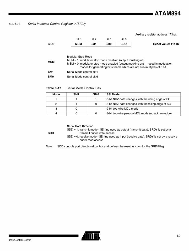
ATAM894
6.3.4.13 Serial Interface Control Register 2 (SIC2)
Note: SDD controls port directional control and defines the reset function for the SRDY-flag
Auxiliary register address: 'A'hex
Bit 3 Bit 2 Bit 1 Bit 0
SIC2 MSM SM1 SM0 SDD Reset value: 1111b
MSM
Modular Stop Mode MSM = 1, modulator stop mode disabled (output masking off) MSM = 0, modulator stop mode enabled (output masking on) — used in modulation modes for generating bit streams which are not sub multiples of 8 bit.
SM1 Serial Mode control bit 1
SM0 Serial Mode control bit 0
Table 6-17. Serial Mode Control Bits
Mode SM1 SM0 SSI Mode
1 1 1 8-bit NRZ-data changes with the rising edge of SC
2 1 0 8-bit NRZ-data changes with the falling edge of SC
3 0 1 9-bit two-wire MCL mode
4 0 0 8-bit two-wire pseudo MCL mode (no acknowledge)
SDD
Serial Data Direction SDD = 1, transmit mode - SD line used as output (transmit data). SRDY is set by a transmit buffer write access SDD = 0, receive mode - SD line used as input (receive data). SRDY is set by a receive buffer read access
694679D–4BMCU–05/05

6.3.4.14 Serial Interface Status and Control Register (SISC)
6.3.4.15 Serial Transmit Buffer (STB) – Byte Write
The STB is the transmit buffer of the SSI. The SSI transfers the transmit buffer into the shift reg-ister and starts shifting with the most significant bit.
Primary register address: 'A'hex
Bit 3 Bit 2 Bit 1 Bit 0
SISC write MCL RACK SIM IFN Reset value: 1111b
SISC read - - - TACK ACT SRDY Reset value: xxxxb
MCL
Multi-Chip Link activation MCL = 1, multi-chip link disabled. This bit has to be set to '0' during transactions to/from the internal EEPROM MCL = 0, connects SC and SD, additionally to the internal multi-chip link pads
RACKReceive ACKnowledge status/control bit for MCL mode RACK = 0, transmit acknowledge in next receive telegram RACK = 1, transmit no acknowledge in last receive telegram
TACKTransmit ACKnowledge status/control bit for MCL mode TACK = 0, acknowledge received in last transmit telegram TACK = 1, no acknowledge received in last transmit telegram
SIMSerial Interrupt Mask SIM = 1, disable interrupts SIM = 0, enable serial interrupt. An interrupt is generated
IFN
Interrupt FuNction IFN = 1, the serial interrupt is generated at the end of telegram IFN = 0, the serial interrupt is generated when the SRDY goes low (i.e., buffer becomes empty/full in transmit/receive mode)
SRDY
Serial interface buffer ReaDY status flag SRDY = 1, in receive mode: receive buffer empty
in transmit mode: transmit buffer full SRDY = 0, in receive mode: receive buffer full
in transmit mode: transmit buffer empty
ACT
Transmission ACTive status flag ACT = 1, transmission is active, i.e., serial data transfer. Stop or start conditions are currently in progress. ACT = 0, transmission is inactive
Primary register address: '9'hex
First write cycle Bit 3 Bit 2 Bit 1 Bit 0 Reset value: xxxxb
Second write cycle Bit 7 Bit 6 Bit 5 Bit 4 Reset value: xxxxb
704679D–4BMCU–05/05
ATAM894

ATAM894
6.3.4.16 Serial Receive Buffer (SRB) – Byte Read
The SRB is the receive buffer of the SSI. The shift register clocks serial data in (most significant bit first) and the loads content into the receive buffer when the complete telegram has been received.
6.3.5 Combination ModesThe UTCM consists of two timers (Timer 2 and Timer 3) and a serial interface. There is a multi-tude of modes in which the timers and serial interface can work together.
The 8-bit wide serial interface operates as shift register for modulation and demodulation. The modulator and demodulator units work together with the timers and shift the data bits into or out of the shift register.
6.3.5.1 Combination Mode Timer 2 and SSI
Figure 6-48. Combination Timer 2 and SSI
Primary register address: '9'hex
First read cycle Bit 7 Bit 6 Bit 5 Bit 4 Reset value: xxxxb
Second read cycle Bit 3 Bit 2 Bit 1 Bit 0 Reset value: xxxxb
4-bit Counter 2/1
RES OVF1
Compare 2/1
T2CO1
POUT
CL2/2DCG
T2M1P4CR
8-bit Counter 2/2
RES OVF2
Compare 2/2
T2CO2T2CM
Timer 2 - control
TOG2
INT4Bi-phase
Manchestermodulator
OUTPUT
MOUT
T2O
Timer 2modulator
output-stage
T2M2
SO Control
T2C
CL2/1
T2I
SYSCLT1OUT
TOG3SCL
I/O-bus
8-bit shift registerMSB LSB
Shift_CL
SO
SIC1 SIC2 SISC
SCLI
Control
STB SRB
SI
Output
INT3
I/O-bus
SSI-control
TOG2
POUTT1OUTSYSCL MCL_SC
MCL_SD
Transmitbuffer
Receivebuffer
CM1
I/O-bus
POUT
SO
SCL
SC
SD
DCGO
TOG2
714679D–4BMCU–05/05
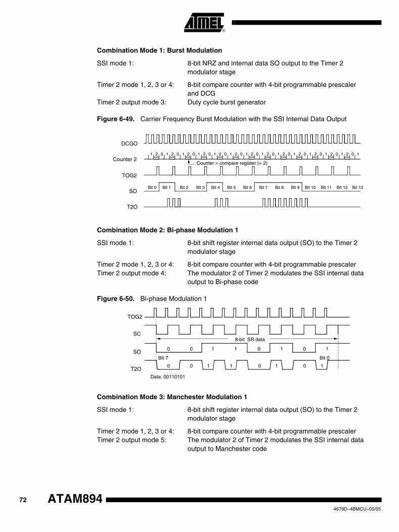
Combination Mode 1: Burst Modulation
SSI mode 1: 8-bit NRZ and internal data SO output to the Timer 2 modulator stage
Timer 2 mode 1, 2, 3 or 4: 8-bit compare counter with 4-bit programmable prescaler and DCG
Timer 2 output mode 3: Duty cycle burst generator
Figure 6-49. Carrier Frequency Burst Modulation with the SSI Internal Data Output
Combination Mode 2: Bi-phase Modulation 1
SSI mode 1: 8-bit shift register internal data output (SO) to the Timer 2 modulator stage
Timer 2 mode 1, 2, 3 or 4: 8-bit compare counter with 4-bit programmable prescaler Timer 2 output mode 4: The modulator 2 of Timer 2 modulates the SSI internal data
output to Bi-phase code
Figure 6-50. Bi-phase Modulation 1
Combination Mode 3: Manchester Modulation 1
SSI mode 1: 8-bit shift register internal data output (SO) to the Timer 2 modulator stage
Timer 2 mode 1, 2, 3 or 4: 8-bit compare counter with 4-bit programmable prescaler Timer 2 output mode 5: The modulator 2 of Timer 2 modulates the SSI internal data
output to Manchester code
1 2 0 1 2 0 1 2 0 1 2 0 1 2 0 1 2 0 1 2 0 1 2 0 1 2 0 1 2 0 1 2 0 1 2 0 1 2 0 1
DCGO
Counter 2
TOG2
SO
T2O
Counter = compare register (= 2)
Bit 0 Bit 1 Bit 2 Bit 3 Bit 4 Bit 5 Bit 6 Bit 7 Bit 8 Bit 9 Bit 10 Bit 11 Bit 12 Bit 13
TOG2
SC
SO
T2O0 0 00
0 0 1 1 0 1 0 1
1 1 1 1
8-bit SR data
Bit 7 Bit 0
Data: 00110101
724679D–4BMCU–05/05
ATAM894
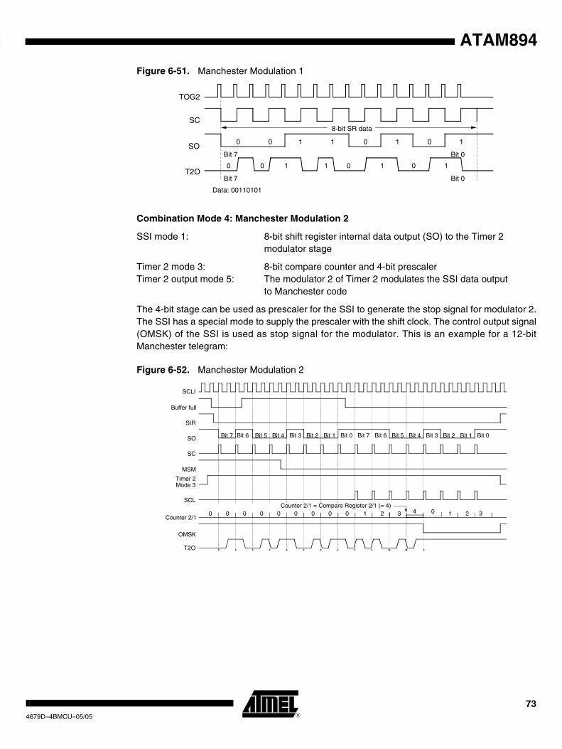
ATAM894
Figure 6-51. Manchester Modulation 1
Combination Mode 4: Manchester Modulation 2
SSI mode 1: 8-bit shift register internal data output (SO) to the Timer 2 modulator stage
Timer 2 mode 3: 8-bit compare counter and 4-bit prescaler Timer 2 output mode 5: The modulator 2 of Timer 2 modulates the SSI data output
to Manchester code
The 4-bit stage can be used as prescaler for the SSI to generate the stop signal for modulator 2. The SSI has a special mode to supply the prescaler with the shift clock. The control output signal (OMSK) of the SSI is used as stop signal for the modulator. This is an example for a 12-bit Manchester telegram:
Figure 6-52. Manchester Modulation 2
TOG2
SC
SO
T2O0 00
0 0 1 1 0 1 0 1
1 1 1 1
8-bit SR data
Bit 7 Bit 0
0
Bit 7 Bit 0
Data: 00110101
0 0 0 0 0 0 0 0 1 2 3 4 0 1 20Counter 2/1 = Compare Register 2/1 (= 4)
Bit 7 Bit 6 Bit 5 Bit 4 Bit 3 Bit 2 Bit 1 Bit 0 Bit 7 Bit 6 Bit 5 Bit 4 Bit 3 Bit 2 Bit 1 Bit 0
SCLI
Buffer full
SIR
SO
SC
MSM
Timer 2Mode 3
SCL
Counter 2/1
OMSK
T2O
3
734679D–4BMCU–05/05
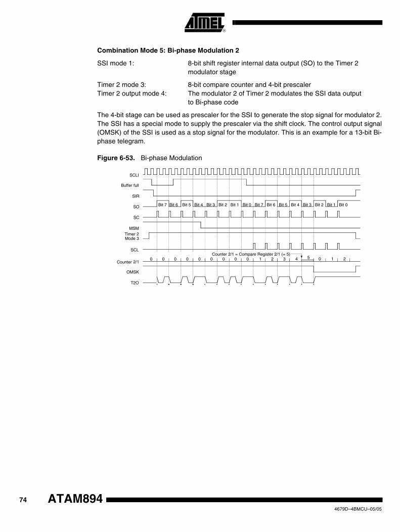
Combination Mode 5: Bi-phase Modulation 2
SSI mode 1: 8-bit shift register internal data output (SO) to the Timer 2 modulator stage
Timer 2 mode 3: 8-bit compare counter and 4-bit prescaler Timer 2 output mode 4: The modulator 2 of Timer 2 modulates the SSI data output
to Bi-phase code
The 4-bit stage can be used as prescaler for the SSI to generate the stop signal for modulator 2. The SSI has a special mode to supply the prescaler via the shift clock. The control output signal (OMSK) of the SSI is used as a stop signal for the modulator. This is an example for a 13-bit Bi-phase telegram.
Figure 6-53. Bi-phase Modulation
0 0 0 0 0 0 0 0 1 2 3 4 50Counter 2/1 = Compare Register 2/1 (= 5)
Bit 7 Bit 6 Bit 5 Bit 4 Bit 3 Bit 2 Bit 1 Bit 0 Bit 7 Bit 6 Bit 5 Bit 4 Bit 3 Bit 2 Bit 1 Bit 0
SCLI
Buffer full
SIR
SO
SC
MSMTimer 2Mode 3
SCL
Counter 2/1
OMSK
T2O
0 1 2
744679D–4BMCU–05/05
ATAM894

ATAM894
6.3.5.2 Combination Mode Timer 3 and SSI
Figure 6-54. Combination Timer 3 and SSI
Combination Mode 6: FSK Modulation
SSI mode 1: 8-bit shift register internal data output (SO) to the Timer 3
Timer 3 mode 8: FSK modulation with shift register data (SO)
The two compare registers are used to generate two varied time intervals. The SSI data output selects which compare register is used for the output frequency generation. A '0'-level at the SSI data output enables the compare register 1 and a '1'-level enables the compare register 2. The compare and compare mode registers must be programmed to generate the two frequencies via the output toggle flip-lop. The SSI can be supplied with the toggle signal of Timer 2 or any other clock source. The Timer 3 counter is driven by an internal or external clock source.
8-bit Counter 3
RES
Compare 3/1
T3CO1
T3CP
T3CO2
Timer 3 - control
T3O
CL3
T3I
T3EXSYSCLT1OUT
POUT
I/O-bus
Compare 3/2
T3CM1 T3CM2
T3C T3ST
Modulator 3
Demodu-lator 3
M2
ControlSO
TOG3
INT5
RES
CM31
T3I
T3EX
SI
SC
T3MT3CS
CP3
8-bit shift registerMSB LSB
Shift_CL
SO
SIC1 SIC2 SISC
SCLI
Control
STB SRB
SI
Output
INT3
I/O-bus
SSI-controlTOG2POUT
T1OUTSYSCL
SI
MCL_SC
MCL_SD
Transmit buffer Receive buffer
SC
SC
SI
754679D–4BMCU–05/05
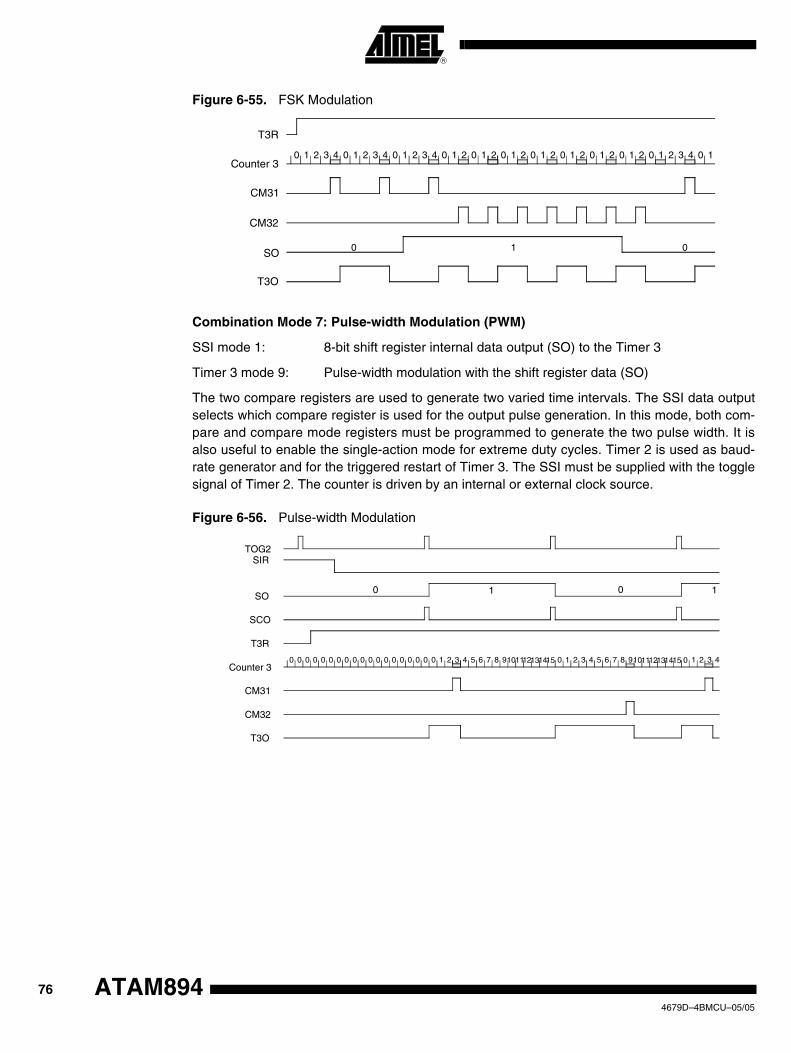
Figure 6-55. FSK Modulation
Combination Mode 7: Pulse-width Modulation (PWM)
SSI mode 1: 8-bit shift register internal data output (SO) to the Timer 3
Timer 3 mode 9: Pulse-width modulation with the shift register data (SO)
The two compare registers are used to generate two varied time intervals. The SSI data output selects which compare register is used for the output pulse generation. In this mode, both com-pare and compare mode registers must be programmed to generate the two pulse width. It is also useful to enable the single-action mode for extreme duty cycles. Timer 2 is used as baud-rate generator and for the triggered restart of Timer 3. The SSI must be supplied with the toggle signal of Timer 2. The counter is driven by an internal or external clock source.
Figure 6-56. Pulse-width Modulation
0 1 2 3 4 0 1 2 3 4 0 1 2 3Counter 3
CM31
CM32
SO
4 0 1 2 0 1 2 0 1 2 0 1 2 0 1 2 0 1 2 0 1 2 0 1 2 3
T3R
4 0
T3O
1
0 1 0
0 0 0 0 0 0 0 0 0 0 0 0 0Counter 3
CM31
CM32
T3O
0 0 0 0 0 1 2 3 4 5 6 7 8 9101112131415 0 1 2 3 4 5
TOG2
6 7 8
1
9 111210 1413 0 2 31 4150
00 1
SIR
SO
SCO
T3R
764679D–4BMCU–05/05
ATAM894

ATAM894
Combination Mode 8: Manchester Demodulation/Pulse-width Demodulation
SSI mode 1: 8-bit shift register internal data input (SI) and the internal shift clock (SCI) from the Timer 3
Timer 3 mode 10: Manchester demodulation/pulse-width demodulation with Timer 3
For Manchester demodulation, the edge detection stage must be programmed to detect each edge at the input. These edges are evaluated by the demodulator stage. The timer stage is used to generate the shift clock for the SSI. A compare register 1 match event defines the correct moment for shifting the state from the input T3I as the decoded bit into the shift register. After that, the demodulator waits for the next edge to synchronize the timer by a reset for the next bit. The compare register 2 can be used to detect a time error and handle it with an interrupt routine.
Before activating the demodulator mode the timer and the demodulator stage must be synchro-nized with the bit-stream. The Manchester code timing consists of parts with the half bit-length and the complete bit-length. A synchronization routine must start the demodulator after an inter-val with the complete bit-length.
The counter can be driven by any internal clock source. The output T3O can be used by Timer 2 in this mode. The Manchester decoder can also be used for pulse-width demodulation. The input must programmed to detect the positive edge. The demodulator and timer must be synchronized with the leading edge of the pulse. After that a counter match with the compare register 1 shifts the state at the input T3I into the shift register. The next positive edge at the input restarts the timer.
Figure 6-57. Manchester Demodulation
1 0 1 1 1 0 0 1 1 0
1 1
BIT 0 BIT 1 BIT 2 BIT 3 BIT 4 BIT 5 BIT 6
Synchronize Manchester demodulation modeTimer 3mode
T3EX
SI
SR-DATA
T3I
CM31 = SCI
1 0 0 1 1 0
774679D–4BMCU–05/05

Combination Mode 9: Bi-phase Demodulation
SSI mode 1: 8-bit shift register internal data input (SI) and the internal shift clock (SCI) from the Timer 3
Timer 3 mode 11: Bi-phase demodulation with Timer 3
In the Bi-phase demodulation mode the timer works like in the Manchester demodulation mode. The difference is that the bits are decoded with the toggle flip-flop. This flip-flop samples the edge in the middle of the bit-frame and the compare register 1 match event shifts the toggle flip-flop output into shift register. Before activating the demodulation the timer and the demodulation stage must be synchronized with the bit-stream. The Bi-phase code timing consists of parts with the half bit-length and the complete bit-length. The synchronization routine must start the demodulator after an interval with the complete bit-length.
The counter can be driven by any internal clock source and the output T3O can be used by Timer 2 in this mode.
Figure 6-58. Bi-phase Demodulation
0 1 1 1 1
0 1
Bit 7 Bit 6 Bit 5 Bit 4 Bit 3 Bit 2 Bit 1
Synchronize Bi-phase demodulation modeTimer 3mode
T3EX
Q1 = SI
CM31 = SCI
SR-DATA
0 0 0 0T3I
ResetCounter 3
1 0 1 0 1 0
Bit 0
784679D–4BMCU–05/05
ATAM894

ATAM894
6.3.5.3 Combination Mode Timer 2 and Timer 3
Figure 6-59. Combination Timer 3 and Timer 2
Combination Mode 10: Frequency Measurement or Event Counter with Time Gate
Timer 2 mode 1/2: 12-bit compare counter/8-bit compare counter and 4-bit prescaler
Timer 2 output mode 1/6: Timer 2 compare match toggles (TOG2) to the Timer 3
Timer 3 mode 3: Timer/Counter; integrated trigger restart and integrated capture (with Timer 2 TOG2-signal)
The counter is driven by an external (T3I) clock source. The output signal (TOG2) of Timer 2 resets the counter. The counter value before reset is saved in the capture register. If single-action mode is activated for one or both compare registers, the trigger signal restarts also the single actions. This mode can be used for frequency measurements or as event counter with time gate.
8-bit Counter 3
RES
Compare 3/1
T3CO1
T3CP
T3CO2
Timer 3 - control
T3O
CL3
T3I
T3EXSYSCLT1OUT
POUT
I/O-bus
Compare 3/2
T3CM1 T3CM2
T3C T3ST
Modulator 3
Demodu-lator 3
ControlSO
TOG3
INT5
RES
CM31
T3I
T3EX
TOG2
SI
SCI
SSI
CP3
4-bit Counter 2/1
RES OVF1
Compare 2/1
T2CO1
CM1
POUT
SSI
CL2/2DCG
T2M1P4CR
8-bit Counter 2/2
RES OVF2
Compare 2/2
T2CO2T2CM
TOG2
INT4Bi-phase
Manchestermodulator
OUTPUT
MOUT
M2
T2O
Timer 2modulator 2output-stage
T2M2
Control(RE, FE, SCO, OMSK)SSI
T2C
CL2/1TOG3
SYSCLT1OUT
SCL
Timer 2 - control
M2
T3CS T3M
POUT
DCGO
SO
T2I
I/O-bus
I/O-bus
794679D–4BMCU–05/05
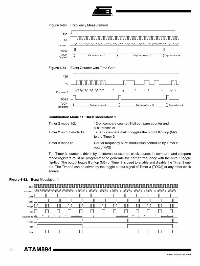
Figure 6-60. Frequency Measurement
Figure 6-61. Event Counter with Time Gate
Combination Mode 11: Burst Modulation 1
Timer 2 mode 1/2: 12-bit compare counter/8-bit compare counter and 4-bit prescaler
Timer 2 output mode 1/6: Timer 2 compare match toggles the output flip-flop (M2) to the Timer 3
Timer 3 mode 6: Carrier frequency burst modulation controlled by Timer 2 output (M2)
The Timer 3 counter is driven by an internal or external clock source. Its compare- and compare mode registers must be programmed to generate the carrier frequency with the output toggle flip-flop. The output toggle flip-flop (M2) of Timer 2 is used to enable and disable the Timer 3 out-put. The Timer 2 can be driven by the toggle output signal of Timer 3 (TOG3) or any other clock source.
Figure 6-62. Burst Modulation 1
0 0 1 2 3 4 5 6 7 8 9 10Counter 3
TOG2T3CP-
Register
T3I
T3R
Capture value = 0 Capture value = 17 Capt. value = 18
11121314151617 1 2 3 4 5 6 7 8 9 1011121314151617180 0 1 2 3 4 5
0 0 1 2 3 4 5 6 7 8 910Counter 3
TOG2
T3CP-Register
11 0 1 2 4 0 1
T3I
23
T3R
Capture value = 0 Capture value = 11 Cap. value = 4
0 1 01 2 3 4 5 0 1 0 1 2 3 4 5 0 10 1 23 4 50 1 01 5 0 1 0 1 5 0 1 0 1 5 0 1 0 1 5 0 1 0 1 5 0 1 0 1 5 0 1 01 5 0 1 01 5 0 1 0 1 5 0 1 01
3 0 1 2 3 3 0 1 32
CL3
Counter 3
CM1
CM2
TOG3
M3
Counter 2/2
TOG2
M2
T3O
804679D–4BMCU–05/05
ATAM894

ATAM894
6.3.5.4 Combination Timer 2, Timer 3 and SSI
Figure 6-63. Combination Timer 2, Timer 3 and SSI
8-bit Counter 3
RES
Compare 3/1
T3CO1
T3CP
T3CO2
Timer 3 - control
T3O
CL3
T3I
T3EXSYSCLT1OUT
POUT
I/O-bus
Compare 3/2
T3CM1 T3CM2
T3C T3ST
Modulator 3
Demodu-lator 3
ControlSO
TOG3
INT5
RES
CM31
T3I
T3EX
TOG2
SI
SCI
SSI
CP3
4-bit Counter 2/1
RES OVF1
Compare 2/1
T2CO1
CM1
POUT
CL2/2DCG
T2M1P4CR
8-bit Counter 2/2
RES OVF2
Compare 2/2
T2CO2T2CM
TOG2
INT4Bi-phase
Manchestermodulator
OUTPUT
MOUT
M2
T2O
Timer 2modulator 2output-stage
T2M2
Control
(RE, FE,SCO, OMSK)
T2C
CL2/1TOG3
SYSCLT1OUT
SCL
Timer 2 - control
M2
T3CS T3M
POUT
DCGO
SO
T2I
I/O-bus
I/O-bus
8-bit shift registerMSB LSBShift_CL
SO
SIC1 SIC2 SISC
SCLI
Control
STB SRB
SI
Output
INT3
I/O-bus
SSI-control
TOG2
POUTT1OUTSYSCL MCL_SC
MCL_SD
Transmit bufferReceivebuffer
SC
SISCL
814679D–4BMCU–05/05

Combination Mode 12: Burst Modulation 2
SSI mode 1: 8-bit shift register internal data output (SO) to the Timer 3
Timer 2 output mode 2: 8-bit compare counter and 4-bit prescaler Timer 2 output mode 1/6: Timer 2 compare match toggles (TOG2) to the SSI
Timer 3 mode 7: Carrier frequency burst modulation controlled by the internal output (SO) of SSI
The Timer 3 counter is driven by an internal or external clock source. Its compare- and compare mode registers must be programmed to generate the carrier frequency with the output toggle flip-flop (M3). The internal data output (SO) of the SSI is used to enable and disable the Timer 3 output. The SSI can be supplied with the toggle signal of Timer 2.
Figure 6-64. Burst Modulation 2
Combination Mode 13: FSK Modulation
SSI mode 1: 8-bit shift register internal data output (SO) to the Timer 3
Timer 2 output mode 3: 8-bit compare counter and 4-bit prescaler Timer 2 output mode 1/6: Timer 2 4-bit compare match signal (POUT) to the SSI
Timer 3 mode 8: FSK modulation with shift register data output (SO)
The two compare registers are used to generate two different time intervals. The SSI data output selects which compare register is used for the output frequency generation. A '0' level at the SSI data output enables the compare register 1 and a '1' level enables the compare register 2. The compare- and compare mode registers must be programmed to generate the two frequencies via the output toggle flip-flop. The SSI can be supplied with the toggle signal of Timer 2 or any other clock source. The Timer 3 counter is driven by an internal or external clock source.
0 1 0 1 2 34 5 0 1 0 1 2 3 45 0 10 1 2 3 4 50 1 0 1 5 0 1 01 5 0 1 01 5 0 1 0 1 5 0 1 0 1 5 0 1 01 5 0 1 0 1 5 0 1 0 1 5 0 1 0 1 5 0 1 01
3 0 1 2 3 3 0 1 32
CL3
Counter 3
CM31
CM32
TOG3
M3
Counter 2/2
TOG2
SO
T3O
824679D–4BMCU–05/05
ATAM894

ATAM894
Figure 6-65. FSK Modulation
7. Data EEPROMThe internal data EEPROM offers 2 pages of 512 bits each. Both pages are organized as 32 × 16 bit words. The programming voltage as well as the write cycle timing is generated on chip.
If it is necessary to be compatible with the ROM parts, only the default page must be used with the flash part. Also for compatibility reasons the access to the EEPROM is handled via the MCL (serial interface) as in the corresponding ROM parts.
The page select is performed by either writing ''01h'' (page 1) or ''09h'' (page 0) to the EEPROM.
Figure 7-1. Block Diagram EEPROM
0 1 2 3 4 0 1 2 3 4 0 1 2 3Counter 3
CM31
CM32
SO
4 0 1 2 0 1 2 0 1 2 0 1 2 0 1 2 0 1 2 0 1 2 0 1 2 3
T3R
4 0
T3O
1
0 1 0
16-bit read/write buffer
Address
control
8-bit data register
EEPROM
2 x 32 x 16
HV-generatorTiming control
Mode
control
I/O
control
SCL
VDD
SDA
Page 1
Page 0
--> write "01h"
--> write "09h"
VSS
834679D–4BMCU–05/05
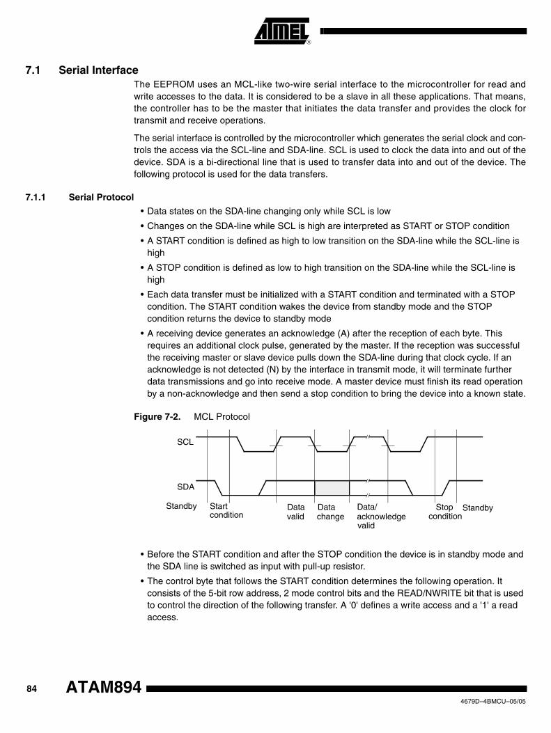
7.1 Serial InterfaceThe EEPROM uses an MCL-like two-wire serial interface to the microcontroller for read and write accesses to the data. It is considered to be a slave in all these applications. That means, the controller has to be the master that initiates the data transfer and provides the clock for transmit and receive operations.
The serial interface is controlled by the microcontroller which generates the serial clock and con-trols the access via the SCL-line and SDA-line. SCL is used to clock the data into and out of the device. SDA is a bi-directional line that is used to transfer data into and out of the device. The following protocol is used for the data transfers.
7.1.1 Serial Protocol
• Data states on the SDA-line changing only while SCL is low
• Changes on the SDA-line while SCL is high are interpreted as START or STOP condition
• A START condition is defined as high to low transition on the SDA-line while the SCL-line is high
• A STOP condition is defined as low to high transition on the SDA-line while the SCL-line is high
• Each data transfer must be initialized with a START condition and terminated with a STOP condition. The START condition wakes the device from standby mode and the STOP condition returns the device to standby mode
• A receiving device generates an acknowledge (A) after the reception of each byte. This requires an additional clock pulse, generated by the master. If the reception was successful the receiving master or slave device pulls down the SDA-line during that clock cycle. If an acknowledge is not detected (N) by the interface in transmit mode, it will terminate further data transmissions and go into receive mode. A master device must finish its read operation by a non-acknowledge and then send a stop condition to bring the device into a known state.
Figure 7-2. MCL Protocol
• Before the START condition and after the STOP condition the device is in standby mode and the SDA line is switched as input with pull-up resistor.
• The control byte that follows the START condition determines the following operation. It consists of the 5-bit row address, 2 mode control bits and the READ/NWRITE bit that is used to control the direction of the following transfer. A '0' defines a write access and a '1' a read access.
Startcondition
Datavalid
Datachange
Data/acknowledgevalid
Stopcondition
SCL
SDA
Standby Standby
844679D–4BMCU–05/05
ATAM894

ATAM894
7.1.1.1 Control Byte Format
7.1.2 EEPROMThe EEPROM has a size of 2 × 512 bits and is organized as 32 x 16-bit matrix each. To read and write data to and from the EEPROM the serial interface must be used. The interface sup-ports one and two byte write accesses and one to n-byte read accesses to the EEPROM.
7.1.2.1 EEPROM - Operating ModesThe operating modes of the EEPROM are defined via the control byte. The control byte contains the row address, the mode control bits and the read/not-write bit that is used to control the direc-tion of the following transfer. A '0' defines a write access and a '1' a read access. The five address bits select one of the 32 rows of the EEPROM memory to be accessed. For all accesses the complete 16-bit word of the selected row is loaded into a buffer. The buffer must be read or overwritten via the serial interface. The two mode control bits C1 and C2 define in which order the accesses to the buffer are performed: High byte – low byte or low byte – high byte. The EEPROM also supports auto increment and auto decrement read operations. After sending the start address with the corresponding mode, consecutive memory cells can be read row by row without transmission of the row addresses.
Two special control bytes enable the complete initialization of EEPROM with '0' or with '1'.
7.1.2.2 Write OperationsThe EEPROM permits 8-bit and 16-bit write operations. A write access starts with the START condition followed by a write control byte and one or two data bytes from the master. It is com-pleted via the STOP condition from the master after the acknowledge cycle.
The programming cycle consists of an erase cycle (write “zeros”) and the write cycle (write “ones”). Both cycles together take about 10 ms.
7.1.2.3 Acknowledge PollingIf the EEPROM is busy with an internal write cycle, all inputs are disabled and the EEPROM will not acknowledge until the write cycle is finished. This can be used to detect the end of the write cycle. The master must acknowledge polling by sending a start condition followed by the control byte. If the device is still busy with the write cycle, it will not return an acknowledge and the mas-ter has to generate a stop condition or perform further acknowledge polling sequences. If the cycle is complete, it returns an acknowledge and the master can proceed with the next read or write cycle.
EEPROM Address Mode Control BitsRead/ NWrite
Start A4 A3 A2 A1 A0 C1 C0 R/NW Ackn
Start Control byte Ackn Data byte Ackn Data byte Ackn Stop
854679D–4BMCU–05/05
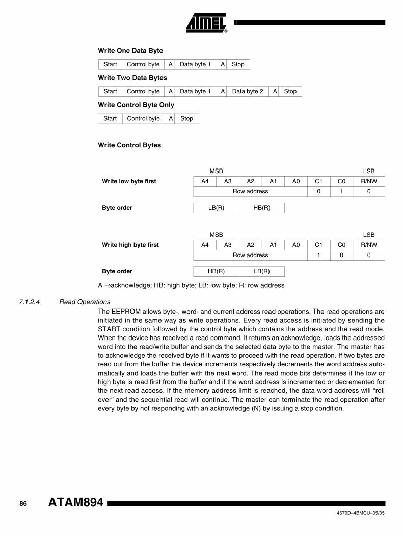
Write One Data Byte
Write Two Data Bytes
Write Control Byte Only
Write Control Bytes
A → acknowledge; HB: high byte; LB: low byte; R: row address
7.1.2.4 Read OperationsThe EEPROM allows byte-, word- and current address read operations. The read operations are initiated in the same way as write operations. Every read access is initiated by sending the START condition followed by the control byte which contains the address and the read mode. When the device has received a read command, it returns an acknowledge, loads the addressed word into the read/write buffer and sends the selected data byte to the master. The master has to acknowledge the received byte if it wants to proceed with the read operation. If two bytes are read out from the buffer the device increments respectively decrements the word address auto-matically and loads the buffer with the next word. The read mode bits determines if the low or high byte is read first from the buffer and if the word address is incremented or decremented for the next read access. If the memory address limit is reached, the data word address will “roll over” and the sequential read will continue. The master can terminate the read operation after every byte by not responding with an acknowledge (N) by issuing a stop condition.
Start Control byte A Data byte 1 A Stop
Start Control byte A Data byte 1 A Data byte 2 A Stop
Start Control byte A Stop
MSB LSB
Write low byte first A4 A3 A2 A1 A0 C1 C0 R/NW
Row address 0 1 0
Byte order LB(R) HB(R)
MSB LSB
Write high byte first A4 A3 A2 A1 A0 C1 C0 R/NW
Row address 1 0 0
Byte order HB(R) LB(R)
864679D–4BMCU–05/05
ATAM894

ATAM894
Read One Data Byte
Read Two Data Bytes
Read n Data Bytes
Read Control Bytes
A → acknowledge, N → no acknowledge; HB: high byte; LB: low byte, R: row address
7.1.2.5 Initializing the Serial Interface to the EEPROMTo prevent unexpected behavior of the EEPROM and its interface it is good practice to use an initialization sequence after any reset of the circuit. This is performed by writing:
to the serial interface. If the EEPROM acknowledges this sequence it is in a defined state. It may be necessary to perform this sequence twice.
Start Control byte A Data byte 1 N Stop
Start Control byte A Data byte 1 A Data byte 2 N Stop
Start Control byte A Data byte 1 A Data byte 2 A - - - Data byte n N Stop
MSB LSB
Read low byte first, address increment
A4 A3 A2 A1 A0 C1 C0 R/NW
Row address 0 1 1
Byte order LB(R) HB(R) LB(R+1) HB(R+1) - - - LB(R+n) HB(R+n)
MSB LSB
Read high byte first, address decrement
A4 A3 A2 A1 A0 C1 C0 R/NW
Row address 1 0 1
Byte order HB(R) LB(R) HB(R-1) LB(R-1) - - - HB(R-n) LB(R-n)
Start “FFh” A N Stop
874679D–4BMCU–05/05
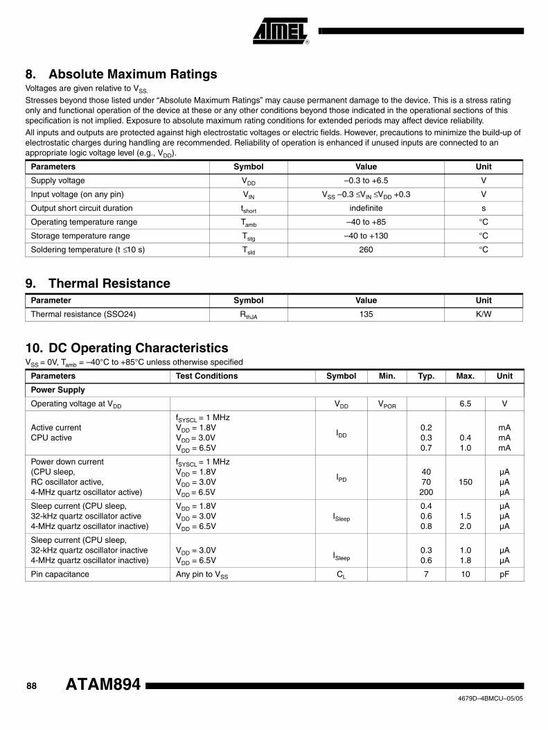
8. Absolute Maximum RatingsVoltages are given relative to VSS.
Stresses beyond those listed under “Absolute Maximum Ratings” may cause permanent damage to the device. This is a stress rating only and functional operation of the device at these or any other conditions beyond those indicated in the operational sections of this specification is not implied. Exposure to absolute maximum rating conditions for extended periods may affect device reliability.All inputs and outputs are protected against high electrostatic voltages or electric fields. However, precautions to minimize the build-up of electrostatic charges during handling are recommended. Reliability of operation is enhanced if unused inputs are connected to an appropriate logic voltage level (e.g., VDD).
Parameters Symbol Value Unit
Supply voltage VDD –0.3 to +6.5 V
Input voltage (on any pin) VIN VSS –0.3 ≤ VIN ≤ VDD +0.3 V
Output short circuit duration tshort indefinite s
Operating temperature range Tamb –40 to +85 °C
Storage temperature range Tstg –40 to +130 °C
Soldering temperature (t ≤ 10 s) Tsld 260 °C
9. Thermal ResistanceParameter Symbol Value Unit
Thermal resistance (SSO24) RthJA 135 K/W
10. DC Operating Characteristics VSS = 0V, Tamb = –40°C to +85°C unless otherwise specified
Parameters Test Conditions Symbol Min. Typ. Max. Unit
Power Supply
Operating voltage at VDD VDD VPOR 6.5 V
Active current CPU active
fSYSCL = 1 MHz VDD = 1.8V VDD = 3.0V VDD = 6.5V
IDD0.20.30.7
0.41.0
mAmAmA
Power down current (CPU sleep, RC oscillator active, 4-MHz quartz oscillator active)
fSYSCL = 1 MHz VDD = 1.8V VDD = 3.0V VDD = 6.5V
IPD4070
200150
µAµAµA
Sleep current (CPU sleep, 32-kHz quartz oscillator active 4-MHz quartz oscillator inactive)
VDD = 1.8V VDD = 3.0V VDD = 6.5V
ISleep
0.40.60.8
1.52.0
µAµAµA
Sleep current (CPU sleep, 32-kHz quartz oscillator inactive 4-MHz quartz oscillator inactive)
VDD = 3.0V VDD = 6.5V
ISleep0.30.6
1.01.8
µAµA
Pin capacitance Any pin to VSS CL 7 10 pF
884679D–4BMCU–05/05
ATAM894

ATAM894
Note: The Pin BP20/NTE has a static pull-up resistor during the reset-phase of the microcontroller
Power-on Reset Threshold Voltage
POR threshold voltage BOT = 1 VPOR 1.54 1.7 1.88 V
POR threshold voltage BOT = 0 VPOR 1.83 2.0 2.20 V
POR hysteresis VPOR 50 mV
Voltage Monitor Threshold Voltage
VM high threshold voltage VDD > VM, VMS = 1 VMThh 3.0 3.35 V
VM high threshold voltage VDD < VM, VMS = 0 VMThh 2.77 3.0 V
VM middle threshold voltage VDD > VM, VMS = 1 VMThm 2.6 2.9 V
VM middle threshold voltage VDD < VM, VMS = 0 VMThm 2.4 2.6 V
VM low threshold voltage VDD > VM, VMS = 1 VMThl 2.2 2.44 V
VM low threshold voltage VDD < VM, VMS = 0 VMThl 2.0 2.2 V
External Input Voltage
VMI VDD = 3V, VMS = 1 VVMI 1.3 1.4 V
VMI VDD = 3V, VMS = 0 VVMI 1.18 1.3 V
All Bi-directional Ports
Input voltage LOW VDD = 1.8 to 6.5V VIL VSS0.2 × VDD
V
Input voltage HIGH VDD = 1.8 to 6.5V VIH0.8 × VDD
VDD V
Input LOW current (switched pull-up)
VDD = 2.0V, VDD = 3.0V, VIL = VSS VDD = 6.5V
IIL
–3–10–80
–8–20–150
–14–40
–240
µAµAµA
Input HIGH current (switched pull-down)
VDD = 2.0V, VDD = 3.0V, VIH = VDD VDD = 6.5V
IIH
31060
620
100
1440
160
µAµAµA
Input LOW current (static pull-up)
VDD = 2.0V VDD = 3.0V, VIL = VSS VDD = 6.5V
IIL
–30–80
–300
–50–160–700
–98–320–1200
µAµAµA
Input LOW current (static pull-down)
VDD = 2.0V VDD = 3.0V, VIH = VDD VDD = 6.5V
IIH
2080300
50160600
100320
1000
µAµAµA
Input leakage current VIL = VSS IIL 100 nA
Input leakage current VIH = VDD IIH 100 nA
Output LOW current
VOL = 0.2 × VDD VDD = 2.0V VDD = 3.0V, VDD = 6.5V
IOL0.938
1.85
15
3.6822
mAmAmA
Output HIGH current
VOH = 0.8 × VDD VDD = 2.0V VDD = 3.0V, VDD = 6.5V
IOH–0.8–3–8
–1.7–5
–15
–3.4–8
–24
mAmAmA
10. DC Operating Characteristics (Continued)VSS = 0V, Tamb = –40°C to +85°C unless otherwise specified
Parameters Test Conditions Symbol Min. Typ. Max. Unit
894679D–4BMCU–05/05

11. AC Characteristics Supply voltage VDD = 1.8 to 6.5V, VSS = 0V, Tamb = 25°C unless otherwise specified.
Parameters Test Conditions Symbol Min. Typ. Max. Unit
Operation Cycle Time
System clock cycle
VDD = 1.8 to 6.5V Tamb = –40 to 85° C
tSYSCL 500 2000 ns
VDD = 2.4 to 6.5V Tamb = –40 to 85° C
tSYSCL 250 2000 ns
Timer 2 input Timing Pin T2I
Timer 2 input clock fT2I 5 MHz
Timer 2 input LOW time Rise/fall time < 10 ns tT2IL 100 ns
Timer 2 input HIGH time Rise/fall time < 10 ns tT2IH 100 ns
Timer 3 Input Timing Pin T3I
Timer 3 input clock fT3I SYSCL/2 MHz
Timer 3 input LOW time Rise/fall time < 10 ns tT3IL 2 tSYSCL ns
Timer 3 input HIGH time Rise/fall time < 10 ns tT3IH 2 tSYSCL ns
Interrupt Request Input Timing
Interrupt request LOW time Rise/fall time < 10 ns tIRL 100 ns
Interrupt request HIGH time Rise/fall time < 10 ns tIRH 100 ns
External System Clock
EXSCL at OSC1, ECM = EN Rise/fall time < 10 ns fEXSCL 0.5 4 MHz
EXSCL at OSC1, ECM = DI Rise/fall time < 10 ns fEXSCL 0.02 4 MHz
Input HIGH time Rise/fall time < 10 ns tIH 0.1 µs
Reset Timing
Power-on reset time VDD > VPOR tPOR 1.5 5 ms
RC-Oscillator 1
Frequency fRcOut1 3.8 MHz
StabilityVDD = 2.0 to 6.5V Tamb = –40 to 85° C
∆f/f ±50 %
RC-Oscillator 2 - External Resistor
Frequency Rext = 180 kΩ fRcOut2 4 MHz
StabilityVDD = 2.0 to 6.5 V Tamb = –40 to 85° C
∆f/f ±15 %
Stabilization time tS 10 µs
4-MHz Crystal Oscillator (Operating Range VDD = 2.2 V to 6.5 V)
Frequency fX 4 MHz
Start-up time tSQ 5 ms
Stability ∆f/f –10 10 ppm
Integrated input/output capacitances (configurable)
CIN/COUT programmable CIN
COUT
0, 2, 5, 7, 10 or 120, 2, 5, 7, 10 or 12
pFpF
904679D–4BMCU–05/05
ATAM894

ATAM894
11.1 Crystal Characteristics
Figure 11-1. Crystal Equivalent Circuit
32-kHz Crystal Oscillator (Operating Range VDD = 2.0V to 6.5V)
Frequency fX 32.768 kHz
Start-up time tSQ 0.5 s
Stability ∆f/f –10 10 ppm
Integrated input/output capacitances (configurable)
CIN/COUT programmable CIN
COUT
0, 2, 5, 7, 10 or 120, 2, 5, 7, 10 or 12
pFpF
External 32-kHz Crystal Parameters
Crystal frequency fX 32.768 kHz
Serial resistance RS 30 50 kΩ
Static capacitance C0 1.5 pF
Dynamic capacitance C1 3 fF
External 4-MHz Crystal Parameters
Crystal frequency fX 4.0 MHz
Serial resistance RS 40 150 Ω
Static capacitance C0 1.4 3 pF
Dynamic capacitance C1 3 fF
Data EEPROM
Operating current during erase/write cycle
IWR 600 1300 µA
EnduranceErase-/write cycles Tamb = 85°C
ED
ED
20000020000
500000CyclesCycles
Data erase/write cycle time For 16-bit access tDEW 9 13 ms
Data retention time Tamb = 85°C
tDR
tDR
10010
yearsyears
Power-up to read operation tPUR 0.2 ms
Power-up to write operation tPUW 0.2 ms
Program EEPROM Erase-/write cycles, Tamb = 0 to 40°C nEW 100 1,000 Cycles
Serial Interface
SCL clock frequency fSC_MCL 100 500 kHz
11. AC Characteristics (Continued)Supply voltage VDD = 1.8 to 6.5V, VSS = 0V, Tamb = 25°C unless otherwise specified.
Parameters Test Conditions Symbol Min. Typ. Max. Unit
LC1 RS
C0
OSCIN OSCOUT
Equivalentcircuit
SCLIN SCLOUT
914679D–4BMCU–05/05

12. EmulationThe basic function of emulation is to test and evaluate the customer's program and hardware in real time. This therefore enables the analysis of any timing, hardware or software problem. For emulation purposes, all MARC4 controllers include a special emulation mode. In this mode, the internal CPU core is inactive and the I/O buses are available via Port 0 and Port 1 to allow an external access to the on-chip peripherals. The MARC4 emulator uses this mode to control the peripherals of any MARC4 controller (target chip) and emulates the lost ports for the application.
The MARC4 emulator can stop and restart a program at specified points during execution, mak-ing it possible for the applications engineer to view the memory contents and those of various registers during program execution. The designer also gains the ability to analyze the executed instruction sequences and all the I/O activities.
Figure 12-1. MARC4 Emulation
MARC4 target chip
CORE(inactive)
Por
t 1P
ort 0
Application-specific hardware
Peripherals
MARC4 emulator
Programmemory
Tracememory
Control logic
Personal computer
CORE
MARC4emulation-CPU
I/O control
I/O bus
Port 0 Port 1SYSCL/
TCL,TE, NRST
Emulation control
Emulator target board
924679D–4BMCU–05/05
ATAM894

ATAM894
14. Package Information
13. Ordering InformationExtended Type Number(1) Program Memory Data-EEPROM Package Delivery
ATAM894x-TNQY 8 kB Flash 2 × 512 Bit SSO24 Taped and reeled
ATAM894x-TNSY 8 kB Flash 2 × 512 Bit SSO24 Tubes
Note: 1. x = Hardware revision Y = Lead-free
technical drawingsaccording to DINspecifications
Package SSO24Dimensions in mm 8.05
7.80
0.150.05
0.25
0.657.15
1.30
5.75.3
4.54.3
6.66.3
0.15
24 13
1 12
934679D–4BMCU–05/05

15. Revision History
Please note that the following page numbers referred to in this section refer to the specific revision mentioned, not to this document.
Revision No. History
4679D-4BMCU-05/05
•Put datasheet in a new template
• Lead-free Logo on page 1 added• Figure 5-2 “ROM Map” on page 5 replaced
• Section “Interrupt Processing” on page 10 changed
• Section “4-MHz Oscillator” on pages 18-19 changed• Section “32-kHz Oscillator” on page 19 changed
• Figure 6-2 “Bi-directional Port 1” on page 25 changed
• Figure 6-3 “Bi-directional Port 2” on page 26 changed• Figure 6-4 “Bi-directional Port 5” on page 27 changed
• Figure 6-6 “Bi-directional Port 4 and Port 6” on page 29 changed
• Table “Ordering Information” on page 93 changed
4679C-4BMCU-03/04
• Put datasheet in a new template• Figure 1 “Block Diagram” on page 1 changed
• Table 9 “Peripheral Addresses” on page 23 changed
• Section “Features” on page 35 changed• Table 19 “Timer 2 Output Select Bits” on page 44 changed
• New heading rows at Table “Absolute Maximum Ratings” on page 86 added
• Table “Thermal Resistance” on page 86 changed• Section “Emulation” on page 90 added
• Table “Ordering Information” on page 91 deleted
• Table “Ordering Information” on page 92 changed
944679D–4BMCU–05/05
ATAM894
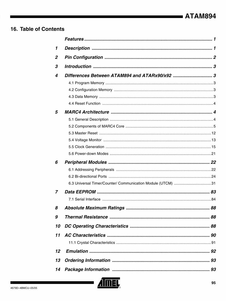
ATAM894
16. Table of Contents
Features ..................................................................................................... 1
1 Description ............................................................................................... 1
2 Pin Configuration ..................................................................................... 2
3 Introduction .............................................................................................. 3
4 Differences Between ATAM894 and ATARx90/x92 ............................... 3
4.1 Program Memory ......................................................................................................3
4.2 Configuration Memory ..............................................................................................3
4.3 Data Memory ............................................................................................................3
4.4 Reset Function .........................................................................................................4
5 MARC4 Architecture ................................................................................ 4
5.1 General Description ..................................................................................................4
5.2 Components of MARC4 Core ...................................................................................5
5.3 Master Reset ..........................................................................................................12
5.4 Voltage Monitor ......................................................................................................13
5.5 Clock Generation ....................................................................................................15
5.6 Power-down Modes ................................................................................................21
6 Peripheral Modules ................................................................................ 22
6.1 Addressing Peripherals ..........................................................................................22
6.2 Bi-directional Ports .................................................................................................24
6.3 Universal Timer/Counter/ Communication Module (UTCM) ...................................31
7 Data EEPROM ......................................................................................... 83
7.1 Serial Interface .......................................................................................................84
8 Absolute Maximum Ratings .................................................................. 88
9 Thermal Resistance ............................................................................... 88
10 DC Operating Characteristics ............................................................... 88
11 AC Characteristics ................................................................................. 90
11.1 Crystal Characteristics ..........................................................................................91
12 Emulation ............................................................................................... 92
13 Ordering Information ............................................................................. 93
14 Package Information ............................................................................. 93
954679D–4BMCU–05/05

15 Revision History ..................................................................................... 94
16 Table of Contents.................................................................................... 95
964679D–4BMCU–05/05
ATAM894

Printed on recycled paper.
4679D–4BMCU–05/05
© Atmel Corporation 2005. All rights reserved. Atmel®, logo and combinations thereof, Everywhere You Are® and others, are registered trade-marks or trademarks of Atmel Corporation or its subsidiaries. Other terms and product names may be trademarks of others.
Disclaimer: The information in this document is provided in connection with Atmel products. No license, express or implied, by estoppel or otherwise, to any intellectual property right is granted by this document or in connection with the sale of Atmel products. EXCEPT AS SET FORTH IN ATMEL’S TERMS AND CONDI-TIONS OF SALE LOCATED ON ATMEL’S WEB SITE, ATMEL ASSUMES NO LIABILITY WHATSOEVER AND DISCLAIMS ANY EXPRESS, IMPLIED OR STATUTORY WARRANTY RELATING TO ITS PRODUCTS INCLUDING, BUT NOT LIMITED TO, THE IMPLIED WARRANTY OF MERCHANTABILITY, FITNESS FOR A PARTICULAR PURPOSE, OR NON-INFRINGEMENT. IN NO EVENT SHALL ATMEL BE LIABLE FOR ANY DIRECT, INDIRECT, CONSEQUENTIAL, PUNITIVE, SPECIAL OR INCIDEN-TAL DAMAGES (INCLUDING, WITHOUT LIMITATION, DAMAGES FOR LOSS OF PROFITS, BUSINESS INTERRUPTION, OR LOSS OF INFORMATION) ARISING OUT OF THE USE OR INABILITY TO USE THIS DOCUMENT, EVEN IF ATMEL HAS BEEN ADVISED OF THE POSSIBILITY OF SUCH DAMAGES. Atmel makes no representations or warranties with respect to the accuracy or completeness of the contents of this document and reserves the right to make changes to specifications and product descriptions at any time without notice. Atmel does not make any commitment to update the information contained herein. Atmel’s products are not intended, authorized, or warranted for use as components in applications intended to support or sustain life.
Atmel Corporation Atmel Operations
2325 Orchard ParkwaySan Jose, CA 95131, USATel: 1(408) 441-0311Fax: 1(408) 487-2600
Regional Headquarters
EuropeAtmel SarlRoute des Arsenaux 41Case Postale 80CH-1705 FribourgSwitzerlandTel: (41) 26-426-5555Fax: (41) 26-426-5500
AsiaRoom 1219Chinachem Golden Plaza77 Mody Road TsimshatsuiEast KowloonHong KongTel: (852) 2721-9778Fax: (852) 2722-1369
Japan9F, Tonetsu Shinkawa Bldg.1-24-8 ShinkawaChuo-ku, Tokyo 104-0033JapanTel: (81) 3-3523-3551Fax: (81) 3-3523-7581
Memory2325 Orchard ParkwaySan Jose, CA 95131, USATel: 1(408) 441-0311Fax: 1(408) 436-4314
Microcontrollers2325 Orchard ParkwaySan Jose, CA 95131, USATel: 1(408) 441-0311Fax: 1(408) 436-4314
La ChantrerieBP 7060244306 Nantes Cedex 3, FranceTel: (33) 2-40-18-18-18Fax: (33) 2-40-18-19-60
ASIC/ASSP/Smart CardsZone Industrielle13106 Rousset Cedex, FranceTel: (33) 4-42-53-60-00Fax: (33) 4-42-53-60-01
1150 East Cheyenne Mtn. Blvd.Colorado Springs, CO 80906, USATel: 1(719) 576-3300Fax: 1(719) 540-1759
Scottish Enterprise Technology ParkMaxwell BuildingEast Kilbride G75 0QR, Scotland Tel: (44) 1355-803-000Fax: (44) 1355-242-743
RF/AutomotiveTheresienstrasse 2Postfach 353574025 Heilbronn, GermanyTel: (49) 71-31-67-0Fax: (49) 71-31-67-2340
1150 East Cheyenne Mtn. Blvd.Colorado Springs, CO 80906, USATel: 1(719) 576-3300Fax: 1(719) 540-1759
Biometrics/Imaging/Hi-Rel MPU/ High Speed Converters/RF Datacom
Avenue de RochepleineBP 12338521 Saint-Egreve Cedex, FranceTel: (33) 4-76-58-30-00Fax: (33) 4-76-58-34-80
Literature Requestswww.atmel.com/literature