Embed Size (px)
Citation preview

IP175G/GI/GH/GHI Data Sheet
1 / 69 November 27, 2012
Copyright © 2012, IC Plus Corp. IP175Gx-DS-R01.3
5 Port 10/100 Ethernet Integrated Switch
(85nm /Extreme Low Power, PWMT®®®® and AFT® ® ® ® )
Features General Description
� 5 port Embedded 10/100 PHY Switch Controller � Support 5 100BaseTX(IP175G) or 4 100Base TX
+ 1 FX(IP175GH) � Support 1K MAC address entry � 448K bits packet buffer memory � 100M PHY support IEEE802.3az at full duplex � 10M PHY only support 10BaseTe � Support Auto MDI-MDIX function � Power Management Tool (PWMT®)
- APS, auto-power saving while Link-off - IEEE 802.3az protocol based power saving - WOL+®, light traffic power saving - PWD, force-off power saving
� Support Auto Factory Test (AFT®) � Single Power 3.3V supply � Built in 1.1V core voltage LDO Regulator � Two Priority queues per port � Support 802.1p & DiffServ based QoS � QoS
- Port base - 802.1p - IP DiffServ IPV4/IPV6 - TCP/UDP port number - Pins configure ports priority (VIP port)
� Support max forwarding packet length 1552/1536 bytes option
� Support port mirror function � Support 1k MAC address � Support broadcast storm protection � Support port trunking (LACP) � Support 16 VLAN (IEEE Std 802.1q)
- Port-based/Tagged-based VLAN - Support insert, remove tag
� Built-in 50 ohm resistors for simplifying BOM � 85nm Process � Package and operation temperature
- IP175G/GH: 48 Pin(6mmx6mm) QFN, 0~70℃
- IP175GI/GHI: 48 Pin(6mmx6mm) QFN, -40~85℃
IP175G/GH is fabricated with advanced CMOS (85nm) technology and only requires a 3.3V sinlge power supply. This feature makes IP175G/GH used very low power consume, such as the full load operation (100Mbps full duplex 5 ports), it only takes 0.45w.
IP175G/GH also supports Power Management Tool (PWMT®) for IEEE 802.3az, APS, WOL+ and PWD for Green Power. While two link devices have no IEEE 802.3az capability, IP175G/GH use WOL+ to change link from 100Mbps to 10Mbps for saving power.
The PWD of IP175G/GH is designed for power down switch immediately by pushing a botton, user don’t plug out the power adapter. Push the botton again, it will power on immediately.
Except Low Power and Rich Power Saving method, IP175G/GH supports AFT® for saving Customer Testing Cost. By using a push bottom and cables, IP175G/GH will Auto test completely by itself.
IP175G/GH/IP175GI/GHI are available in 48 QFN lead free package.
Application � 5 port 10/100 Dumb swith � 4TX+1FX Dumb Switcn

IP175G/GI/GH/GHI Data Sheet
2 / 69 November 27, 2012
Copyright © 2012, IC Plus Corp. IP175Gx-DS-R01.3
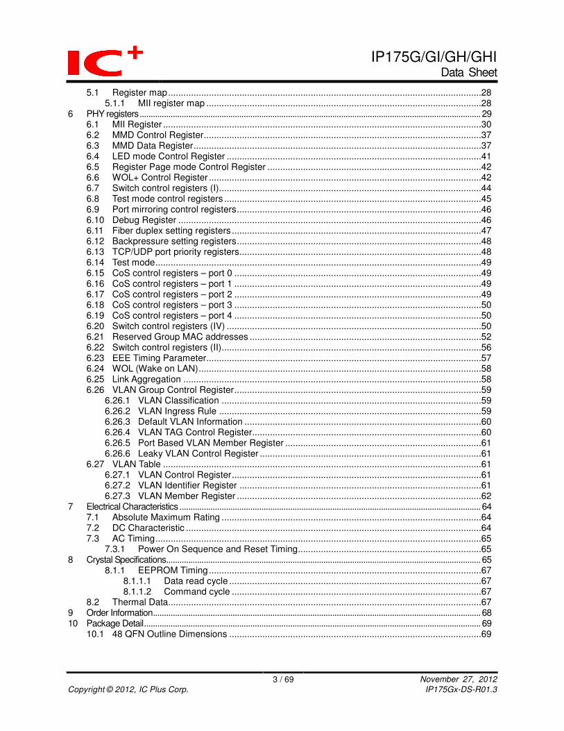
Table of Contents
Features............................................................................................................................................................................. 1 General Description.......................................................................................................................................................... 1 Table of Contents .............................................................................................................................................................. 2 List of Tables...................................................................................................................................................................... 4 List of Figures.................................................................................................................................................................... 5 Revision History ................................................................................................................................................................ 6 1 Pin diagram............................................................................................................................................................... 7
1.1 IP175G/GH Pin diagram (QFN48) ............................................................................................7 2 IP175G/GH application diagram ............................................................................................................................. 8
2.1 An 5 TP port switch application.................................................................................................8 2.2 An 5-port switch mixed with a fiber port ....................................................................................8
3 Pin description........................................................................................................................................................... 9 3.1 Analog pins ...............................................................................................................................9 3.2 MDI (Media Dependent Interface).............................................................................................9 3.3 System clock & reset pins .......................................................................................................10 3.4 Boundry scan & test mode......................................................................................................10 3.5 EEPROM interface /SMI (Serial Management interface)........................................................11 3.6 Miscellaneous setting pins ......................................................................................................12 3.7 LED interface ..........................................................................................................................13 3.8 Power & ground pads..............................................................................................................13
4 Functional Description............................................................................................................................................14 4.1 Switch Engine and Queue Management ................................................................................14
4.1.1 Switch Engine ...............................................................................................................14 4.1.2 Packet Forwarding ........................................................................................................14 4.1.3 Flow control...................................................................................................................14 4.1.4 Backpressure ................................................................................................................14 4.1.5 Broadcast storm protection ...........................................................................................14
4.2 Rserved Group MAC Address.................................................................................................15 4.3 Green Power ...........................................................................................................................16
4.3.1 Auto Power Saving Mode .............................................................................................16 4.3.2 IEEE802.3az EEE (Energy Efficient Ethernet) .............................................................16 4.3.3 WOL+ (Wake On LAN Plus) .........................................................................................16
4.4 Force Power Off ......................................................................................................................17 4.5 Auto Factory Test (AFT) Mode ................................................................................................18 4.6 Reset .......................................................................................................................................18 4.7 Serial management interface ..................................................................................................19 4.8 CoS .........................................................................................................................................20
4.8.1 Port base priority ...........................................................................................................20 4.8.2 Frame base priority .......................................................................................................20
4.8.2.1 VLAN tag and TCP/IP TOS.................................................................................20 4.8.2.2 IPv4/IPv6 DiffServ...............................................................................................21 4.8.2.3 TCP/UDP logical port priority ..............................................................................22
4.9 Port Mirroring ..........................................................................................................................22 4.10 Link Aggergation .....................................................................................................................23 4.11 Buffer Aging.............................................................................................................................25 4.12 LED display (normal operation) ..............................................................................................25 4.13 Serial LED Mode .....................................................................................................................25
4.13.1 Supports link LED only..................................................................................................25 4.13.2 Supports link, speed, and duplex LED..........................................................................26
4.14 LED Blink Timing.....................................................................................................................26 4.15 PAD Driving Calibration...........................................................................................................26 4.16 Fiber port configuration ...........................................................................................................27
5 Register descriptions..............................................................................................................................................28
IP175G/GI/GH/GHI Data Sheet
3 / 69 November 27, 2012
Copyright © 2012, IC Plus Corp. IP175Gx-DS-R01.3
5.1 Register map...........................................................................................................................28 5.1.1 MII register map ............................................................................................................28
6 PHY registers..........................................................................................................................................................29 6.1 MII Register .............................................................................................................................30 6.2 MMD Control Register.............................................................................................................37 6.3 MMD Data Register.................................................................................................................37 6.4 LED mode Control Register ....................................................................................................41 6.5 Register Page mode Control Register ....................................................................................42 6.6 WOL+ Control Register ...........................................................................................................42 6.7 Switch control registers (I).......................................................................................................44 6.8 Test mode control registers .....................................................................................................45 6.9 Port mirroring control registers................................................................................................46 6.10 Debug Register .......................................................................................................................46 6.11 Fiber duplex setting registers..................................................................................................47 6.12 Backpressure setting registers................................................................................................48 6.13 TCP/UDP port priority registers...............................................................................................48 6.14 Test mode................................................................................................................................49 6.15 CoS control registers – port 0 .................................................................................................49 6.16 CoS control registers – port 1 .................................................................................................49 6.17 CoS control registers – port 2 .................................................................................................49 6.18 CoS control registers – port 3 .................................................................................................50 6.19 CoS control registers – port 4 .................................................................................................50 6.20 Switch control registers (IV) ....................................................................................................50 6.21 Reserved Group MAC addresses ...........................................................................................52 6.22 Switch control registers (II)......................................................................................................56 6.23 EEE Timing Parameter............................................................................................................57 6.24 WOL (Wake on LAN)...............................................................................................................58 6.25 Link Aggregation .....................................................................................................................58 6.26 VLAN Group Control Register.................................................................................................59
6.26.1 VLAN Classification ......................................................................................................59 6.26.2 VLAN Ingress Rule .......................................................................................................59 6.26.3 Default VLAN Information .............................................................................................60 6.26.4 VLAN TAG Control Register..........................................................................................60 6.26.5 Port Based VLAN Member Register .............................................................................61 6.26.6 Leaky VLAN Control Register .......................................................................................61
6.27 VLAN Table .............................................................................................................................61 6.27.1 VLAN Control Register..................................................................................................61 6.27.2 VLAN Identifier Register ...............................................................................................61 6.27.3 VLAN Member Register ................................................................................................62
7 Electrical Characteristics ........................................................................................................................................64 7.1 Absolute Maximum Rating ......................................................................................................64 7.2 DC Characteristic ....................................................................................................................64 7.3 AC Timing................................................................................................................................65
7.3.1 Power On Sequence and Reset Timing........................................................................65 8 Crystal Specifications..............................................................................................................................................65
8.1.1 EEPROM Timing...........................................................................................................67 8.1.1.1 Data read cycle ...................................................................................................67 8.1.1.2 Command cycle ..................................................................................................67
8.2 Thermal Data...........................................................................................................................67 9 Order Information....................................................................................................................................................68 10 Package Detail........................................................................................................................................................69
10.1 48 QFN Outline Dimensions ...................................................................................................69

IP175G/GI/GH/GHI Data Sheet
4 / 69 November 27, 2012
Copyright © 2012, IC Plus Corp. IP175Gx-DS-R01.3
List of Tables
Table 1 Pin description ............................................................................................................... 9 Table 2 Rserved Group MAC Address table............................................................................. 15 Table 3 TCP/UDP logical port priority table .............................................................................. 22 Table 4 LED Blink Timing.......................................................................................................... 26 Table 5 Fiber port Parameter.................................................................................................... 27 Table 6 MII register map table .................................................................................................. 28 Table 7 PHY Register Map ....................................................................................................... 29 Table 8 MMD Control Register table......................................................................................... 37 Table 9 MMD Data Register table............................................................................................. 37 Table 10 LED mode Control Register table .............................................................................. 41 Table 11 Register Page mode Control Register table .............................................................. 42 Table 12 WOL+ Control Register table..................................................................................... 42 Table 13 Switch control registers (I) table................................................................................. 44 Table 14 Test mode control registers table ............................................................................... 45 Table 15 Port mirroring control registers table.......................................................................... 46 Table 16 Debug Register table ................................................................................................. 46 Table 17 Fiber duplex setting registers table............................................................................ 47

IP175G/GI/GH/GHI Data Sheet
5 / 69 November 27, 2012
Copyright © 2012, IC Plus Corp. IP175Gx-DS-R01.3
List of Figures
Figure 1 Pin Diagram ..................................................................................................................7 Figure 2 Application Diagram......................................................................................................8 Figure 3 WOL+ Application Diagram.........................................................................................17 Figure 4 Magic Packet Format ..................................................................................................17 Figure 5 Force Power Off Application Diagram.........................................................................17 Figure 6 Auto Factory Test Application Diagram.......................................................................18 Figure 7 Serial management interface Read / Write Diagram ..................................................19 Figure 8 VLAN tag and TCP/IP TOS frame...............................................................................20 Figure 9 IPv4/IPv6 DiffServ frame.............................................................................................21 Figure 10 Port Mirroring Security Block Diagram......................................................................23 Figure 11 Trunk Channel Behavior Block Diagram ...................................................................23 Figure 12 Load Balance Block Diagram....................................................................................24 Figure 13 Serial LED Link/Activity Mode...................................................................................25 Figure 14 Serial LED Fully Mode ..............................................................................................26

IP175G/GI/GH/GHI Data Sheet
6 / 69 November 27, 2012
Copyright © 2012, IC Plus Corp. IP175Gx-DS-R01.3
Revision History
Revision # Date Change Description
IP175G-DS-R01 2012/07/06 Initial release
IP175G-DS-R01.1 2012/10/01 Add 1.1V power pin description – page 13
IP175Gx-DS-R01.2 2012/11/14 1. Add IP175GH description for fiber application. 2. Modify 1.1V maxima value to 1.23V – page 62 3. Add MAC address entry and buffer size description – page 1 4. Add Serial LED Mode description – page 25
IP175Gx-DS-R01.3 2012/11/27 1. Delete default VLAN Information TPID description – page 60

IP175G/GI/GH/GHI Data Sheet
7 / 69 November 27, 2012
Copyright © 2012, IC Plus Corp. IP175Gx-DS-R01.3
1 Pin diagram
1.1 IP175G/GH Pin diagram (QFN48)
(6mm X 6mm Top view)
Exposed pad (pad 49) is system GND, must be soldered to PCB ground plane
Figure 1 Pin Diagram
AV
10
RX
IP3
RX
IM3
TX
OP
3
TX
OM
3
AV
33
TX
OM
4
TX
OP
4
RX
IM4
RX
IP4
OS
CI
X2
TXOP2
TXOM1
TXOP1
RXIM1
RXIP1
BGRES
AV33
PLLGND
PLLVCC
RXIP2]RXIM2
TXOM2
13
14
15
16
17
18
19
20
21
22
23
24
1
2
3
4
5
6
7
8
9
10
11
12
36
35
34
33
32
31
30
29
28
27
26
25
48
47
46
45
44
43
42
41
40
39
38
37
49 E-Pad Ground
AV
33
TX
OM
0
TX
OP
0
RX
IM0
RX
IP0
AV
10
PV
DD
_LD
O
VR
EG
_LD
O
DV
DD
SD
A/M
DIO
SC
L/M
DC
LIN
K_LE
D0/S
DA
TA
/CO
S_D
IS
LINK_LED1/SCLK/BF_STM_DIS
LINK_LED2/RSVD_GMAC_FILTER
PVDD
LINK_LED3
LINK_LED4
F_POWER_OFF_LED / VLAN_DIS
AUTO_FACTORY_TEST
TEST
F_POWER_OFF
DVDD
RESETB
FXSD4 (IP175GH) / GND (IP175G)

IP175G/GI/GH/GHI Data Sheet
8 / 69 November 27, 2012
Copyright © 2012, IC Plus Corp. IP175Gx-DS-R01.3
2 IP175G/GH application diagram
2.1 An 5 TP port switch application
Here shows the application diagram of 5-port switch. 2.2 An 5-port switch mixed with a fiber port
Figure 2 Application Diagram
PHY 0
IP178GH
PHY 1 PHY 2 PHY 3 PHY 4 PHY 5 PHY 6 PHY 7
Switch engine
MAC 0 MAC 1 MAC 2 MAC 3 MAC 4 MAC 5 MAC 6 MAC 7
IP175GH P0 P1 P2 P3 P4
TP Fiber MAU
PHY 0
IP178G
PHY 1 PHY 2 PHY 3 PHY 4 PHY 5 PHY 6 PHY 7
Switch engine
MAC 1 MAC 2 MAC 3 MAC 4 MAC 5 MAC 6 MAC 7
IP175G P0 P1 P2 P3 P4
TP
MAC 0

IP175G/GI/GH/GHI Data Sheet
9 / 69 November 27, 2012
Copyright © 2012, IC Plus Corp. IP175Gx-DS-R01.3
3 Pin description
Table 1 Pin description
Type Description Type Description
I Input pin IPL Input pin with internal pull low 100K ohm
O Output pin IPH Input pin with internal pull high 200K ohm
P Power or Ground
3.1 Analog pins
Pin No. Label Type Description
LDO Regulator
41 VREG_LDO P LDO regulator output It is an output power pin for 1.1V power source.
42 PVDD_LDO P LDO regulator input It is an input power pin for reference voltage.
IP176G includes a LDO regulator to convert 3.3V to 1.1V.
3.2 MDI (Media Dependent Interface)
Pin No. Label Type Description
Transceiver
44, 45, 3, 4, 8, 9,
14, 15, 22, 21
RXIP0, RXIM0, RXIP1, RXIM1, RXIP2, RXIM2, RXIP3, RXIM3, RXIP4, RXIM4
I TP receive
46, 47, 2, 1,
10, 11, 16, 17, 20, 19
TXOP0, TXOM0, TXOP1, TXOM1, TXOP2, TXOM2, TXOP3, TXOM3, TXOP4, TXOM4
O TP transmit
25
FXSD4 GND
I
P
Fiber signal detection of port 4 (IP175GH) Port 4 can be configured to be either a TP port or a Fiber port with this pin. Connect this pin to GND for TP mode, and do not left this pin floating. Please refer to the paragraph “I/O Electrical Characteristics” for more detail information. It is GND pin (IP175G.)
5 BGRES O
Band gap resistor. It is connected GND through a precision resistor (R=6.19K, 1%) for band gap reference. Please refer to application circuit for more information.

IP175G/GI/GH/GHI Data Sheet
10 / 69 November 27, 2012
Copyright © 2012, IC Plus Corp. IP175Gx-DS-R01.3
3.3 System clock & reset pins
Pin No.
Label Type Description
23 OSCI I
25MHz system clock It is recommended to connect OSCI and X2 to a 25MHz crystal. If the clock source is from another chip or oscillator, the clock should be active at least for 1ms before pin 25 RESETB de-asserted. Pin 24 X2 should be left open in this application.
24 X2 O Crystal pin A 25Mhz crystal can be connected to OSCI and X2.
25 RESETB I
Reset It is a low active input pad with Schmitt trigger. The reset time must be hold for more than 10 ms. If an R/C reset circuit is used, the capacitor should be connected to PVDD as shown in the figure.
3.4 Boundry scan & test mode
Pin No.
Label Type Description
29 TEST I Test mode enable It should be connected to GND for normal operation
30 AUTO_FACTORY_TEST
IPL Auto Factory Test (AFT®) enable pin
RESETB
R
PVDD
C

IP175G/GI/GH/GHI Data Sheet
11 / 69 November 27, 2012
Copyright © 2012, IC Plus Corp. IP175Gx-DS-R01.3
3.5 EEPROM interface /SMI (Serial Management interface)
Pin No. Label Type Description
EEPROM (only 24C02, 24C04, 24C08 & 24C16 supported)
38 SCL/MDC IPL/I
After reset, it is used as clock pin SCL of EEPROM. Its period is longer than 10us. IP175G/GH stops reading EEPROM if it finds there is no 0x55AA pattern in address 0. After reading EEPROM, this pin will switch to SMI mode MDC input.
39 SDA/MDIO IPH, I/O
After reset, it is used as data pin SDA of EEPROM. A bi-directional multi-drop bus for accessing the internal registers. It’s recommended to add a 4.7K pull up resistor connecting to PVDD and a 30pf capacitor connecting to ground. After reading EEPROM, this pin will switch to SMI mode MDIO for read/write internal register.

IP175G/GI/GH/GHI Data Sheet
12 / 69 November 27, 2012
Copyright © 2012, IC Plus Corp. IP175Gx-DS-R01.3
3.6 Miscellaneous setting pins
Pin No. Label Type Description
Misc.
28 F_POWER_OFF IPH/I
Force Power Off function for power saving setting pin It should be connected to PVDD for normal operation; pull low 3 seconds to enable Force Power Off function.
31 VLAN_DIS IPH/O
Home VLAN setting enable setting pin. Port 0~Port 3 are all individual VLAN and only send to port 4. 1: disable (default) 0: enable It is an input signal during reset and its value is latched at the end of reset. This pin acts as a F_POWER_OFF_LED after reset
35 REVD_GMAC_FILTER IPH/O
Reserved group address filtering It configures how to process the reserved group address, detail see 4.2.
36 BF_STM_DIS IPH/O
Broadcast storm protection enable This function defined in MII register 20.1.[6] 1: disable (default) 0: enable A port begins to drop incoming packets if it receives broadcast packets more than the threshold defined in MII register 20.9.[15,14] It is an input signal during reset and its value is latched at the end of reset. This pin acts as a link LED of port 1 after reset
37 COS_EN IPH/O
Class of service enable Packets with high priority tag are handled as high priority packets if the function is enabled. 1: disabled (default) 0: enable, It is an input signal during reset and its value is latched at the end of reset. It acts as a link LED of port 0 after reset.
IP175G/GI/GH/GHI Data Sheet
13 / 69 November 27, 2012
Copyright © 2012, IC Plus Corp. IP175Gx-DS-R01.3
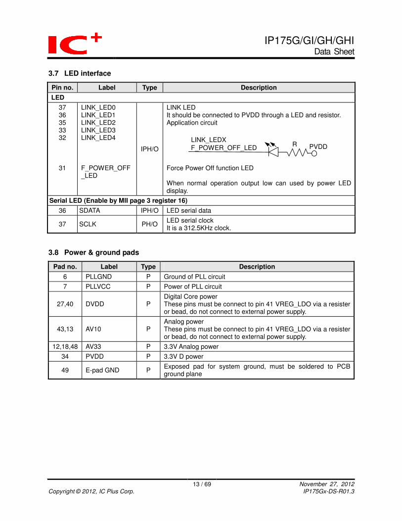
3.7 LED interface
Pin no. Label Type Description
LED
37 36 35 33 32
31
LINK_LED0 LINK_LED1 LINK_LED2 LINK_LED3 LINK_LED4 F_POWER_OFF_LED
IPH/O
LINK LED It should be connected to PVDD through a LED and resistor. Application circuit Force Power Off function LED When normal operation output low can used by power LED display.
Serial LED (Enable by MII page 3 register 16)
36 SDATA IPH/O LED serial data
37 SCLK PH/O LED serial clock It is a 312.5KHz clock.
3.8 Power & ground pads
Pad no. Label Type Description
6 PLLGND P Ground of PLL circuit
7 PLLVCC P Power of PLL circuit
27,40 DVDD P Digital Core power These pins must be connect to pin 41 VREG_LDO via a resister or bead, do not connect to external power supply.
43,13 AV10 P Analog power These pins must be connect to pin 41 VREG_LDO via a resister or bead, do not connect to external power supply.
12,18,48 AV33 P 3.3V Analog power
34 PVDD P 3.3V D power
49 E-pad GND P Exposed pad for system ground, must be soldered to PCB ground plane
F_POWER_OFF_LED
R PVDD LINK_LEDX

IP175G/GI/GH/GHI Data Sheet
14 / 69 November 27, 2012
Copyright © 2012, IC Plus Corp. IP175Gx-DS-R01.3
4 Functional Description
4.1 Switch Engine and Queue Management
4.1.1 Switch Engine
IP175G/GH integrates an 5-port switch controller, SSRAM, and 5 10/100 Ethernet transceivers. Each of the transceivers complies with the IEEE 802.3, IEEE 802.3u, and IEEE 802.3x specifications. IP175G/GH offers all the rich features of a high-speed broadband wire Internet services including non-blocking switch fabric
4.1.2 Packet Forwarding
IP175G/GH utilizes the “store & forward” method to handle packet transfer. IP175G/GH begins to forward a packet to a destination port after the entire packet is received. A received packet will be forwarded to the destination port only if it is error free; otherwise, it will be discarded.
4.1.3 Flow control
IP175G/GH jams or pauses a port, which causes output queue over the threshold. Its link partner will defer transmission after detecting the jam or pause frame. A port of IP175G/GH defers transmission when it receives a jam or a pause frame. The source address (SA) of pause control frame will be [ IP175G/GH OUI (0090C3), port number]. For example, the SA of port 1 pause control frame will be “ 00 90 C3 00 00 01”. When CoS is enabled, IP175G/GH may disable the flow control function for a short term to guarantee the bandwidth of high priority packets. A port disables its flow control function for 2 ~ 3 seconds when it receives a high priority packet. It doesn’t transmit pause frame or jam pattern during the period but it still responses to pause frame or jam pattern.
4.1.4 Backpressure
In half duplex mode, the IP175G/GH supports backpressure flow control. When set BK_EN of MII register 20.1[8] to “1”, the packets in buffer reach the threshold, IP175G/GH generates a jam pattern to back off the link partner. IP175G/GH supports carrier-sense based backpressure. When the carrier-sense based backpressure is enabled, MII register 20.1[7] is set to “0”, and IP175G/GH transmits null packets continuously to prevent link partner’s transmission when the buffer is not available.
4.1.5 Broadcast storm protection
A port of IP175G/GH begins to drops broadcast packets if the received broadcast packets are more than the threshold defined in MII register 21.9[15:14] BF_STM_THR_SEL [1:0] in 10ms (100Mbps) or 100ms (10Mbps)
The function can be enabled by pulling low pin 36 BF_STM_DIS or programming MII register 20.1[6].
IP175G/GH handles multicast frame as a broadcast frame in broadcast storm protection function if MII register 21.30[12] is set to “0”
IP175G/GI/GH/GHI Data Sheet
15 / 69 November 27, 2012
Copyright © 2012, IC Plus Corp. IP175Gx-DS-R01.3
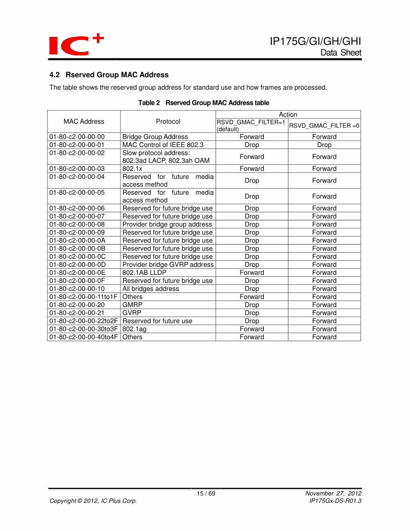
4.2 Rserved Group MAC Address
The table shows the reserved group address for standard use and how frames are processed.
Table 2 Rserved Group MAC Address table
Action MAC Address Protocol RSVD_GMAC_FILTER=1
(default) RSVD_GMAC_FILTER =0
01-80-c2-00-00-00 Bridge Group Address Forward Forward
01-80-c2-00-00-01 MAC Control of IEEE 802.3 Drop Drop
01-80-c2-00-00-02 Slow protocol address: 802.3ad LACP, 802.3ah OAM
Forward Forward
01-80-c2-00-00-03 802.1x Forward Forward
01-80-c2-00-00-04 Reserved for future media access method
Drop Forward
01-80-c2-00-00-05 Reserved for future media access method
Drop Forward
01-80-c2-00-00-06 Reserved for future bridge use Drop Forward
01-80-c2-00-00-07 Reserved for future bridge use Drop Forward
01-80-c2-00-00-08 Provider bridge group address Drop Forward
01-80-c2-00-00-09 Reserved for future bridge use Drop Forward
01-80-c2-00-00-0A Reserved for future bridge use Drop Forward
01-80-c2-00-00-0B Reserved for future bridge use Drop Forward
01-80-c2-00-00-0C Reserved for future bridge use Drop Forward
01-80-c2-00-00-0D Provider bridge GVRP address Drop Forward
01-80-c2-00-00-0E 802.1AB LLDP Forward Forward
01-80-c2-00-00-0F Reserved for future bridge use Drop Forward
01-80-c2-00-00-10 All bridges address Drop Forward
01-80-c2-00-00-11to1F Others Forward Forward
01-80-c2-00-00-20 GMRP Drop Forward
01-80-c2-00-00-21 GVRP Drop Forward
01-80-c2-00-00-22to2F Reserved for future use Drop Forward
01-80-c2-00-00-30to3F 802.1ag Forward Forward
01-80-c2-00-00-40to4F Others Forward Forward

IP175G/GI/GH/GHI Data Sheet
16 / 69 November 27, 2012
Copyright © 2012, IC Plus Corp. IP175Gx-DS-R01.3
4.3 Green Power
IP175G/GH provides various power management modes to save the power consumption. In addition to the power down mode defined on IEEE802.3, two extra power saving modes are used to further reduce the system power consumption.
4.3.1 Auto Power Saving Mode
IP175G/GH will automatically enter this mode if no cable link is established. After entering this mode, IP175G/GH will shutdown unnecessary function and issue the link pulse at a rate lower than the regular rate specified on IEEE 802.3.
4.3.2 IEEE802.3az EEE (Energy Efficient Ethernet)
In order to enter this mode, the PHY part should declare the EEE capability during the auto-negotiation phase.
It’s the higher layer’s responsibility to memorize the link partner’s wakeup time and wakeup the link partner before sending data. The higher layer means a mechanism that can evaluate the packet buffer utilization and wake the link partner before sending the data. In general speaking, this mechanism probably consists of at least one of the following items: the packet buffer manager, the application program and OS.
The EEE module works well at LPI (Low Power Idle) mode when 1. Link at full-duplex and 2. Auto-negotiation is enabled in both local and remote PHYs and 3. 100Mbps full duplex and 4. EEE ability is supported in both local & remote PHYs and 5. EEE_EN (Reg 22.0[7:0]) is enabled for EEE function via default value and 6. SLEEP_TIMER (Reg 22.1[11:0]) is the default value for EEE sleep timer and 7. WAKE_TIME (Reg 22.2~9) is the default value for EEE wake time.
4.3.3 WOL+ (Wake On LAN Plus)
IP175G/GH not only consumes low power, but also provides various energy-saving methods to save the power. These combined methods make IP175G/GH a “green” PHY. The following pictures show the method.
Packet wakes it up
No-Traffic leads it to sleep
IP175G
IP175G

IP175G/GI/GH/GHI Data Sheet
17 / 69 November 27, 2012
Copyright © 2012, IC Plus Corp. IP175Gx-DS-R01.3
Figure 3 WOL+ Application Diagram
The IP175G/GH WOL+ function will be active if a port’s RX is in idle state for a period time and this port WOL+ function is enabled (by Reg 20.10[15:8]). This period time can be configured by WOL+ timer register (Reg22.10).
This port will be wake up if a) Sense magic packet; b) Sense link change; c) Sense any packet;
The packet format of Magic packet is showing as follows, source address=0x112233445566 for example, repeat this source address 16 times at least.
Received Packet
0xFFFFFFFFFFFF
0X112233445566
0X112233445566
0X112233445566
0X112233445566
0X112233445566
0X112233445566
Figure 4 Magic Packet Format
4.4 Force Power Off
When “Force power off enable” (pin 28) is pull low for 3 seconds,IP175G/GH will enter force power off mode.If “Force power off enable” pin pull low for 3 seconds again, IP175G/GH will return normal mode. The expired timer (default value is 3 seconds) is configurable in “FORCE_POWER_OFF_TIME” (MII Register 21.10[7:6]).
Figure 5 Force Power Off Application Diagram
>16 times
Force ON / OFF
( rBOM = 1 push buttom,the others take care by the chip.)
IP175G

IP175G/GI/GH/GHI Data Sheet
18 / 69 November 27, 2012
Copyright © 2012, IC Plus Corp. IP175Gx-DS-R01.3
4.5 Auto Factory Test (AFT) Mode
IP175G/GH implements an AFT mechanism, which is very useful for switch pre-test as Figure 5 AFT system diagrams. When this function is triggered by hardware pin AFT, IP175G/GH physical ports are connected either port-pairs loopback or self-loopback and then IP175G/GH will generate frames for TX of all ports and LED will flash.
For example, port1 and port2 are connected to each other (loopback). Check the LED of port1 and port2 is light-on, and then trigger this AFT function and wait a moment trigger again. If the test result is passed (no CRC or packet loss), show LED of port1 and port2 light-on. Otherwise, show LED light-off when CRC or packet loss is happened. Procedure: 1. Power On 2. Wait for someone Push AFT button to start test 3. IP175G/GH transmit packet and LED flash 4. If Push AFT button then goto step 5, else goto step 3 5. LED Show the test result, goto step 2
Figure 6 Auto Factory Test Application Diagram 4.6 Reset
Hardware Reset: Hardware pin RESETB should be asserted LOW at least for 10ms to reset IP175G/GH, and gets initial values from pins, registers and EEPROM after reset.
IP175G
P0 P1 P2 P3 P4
AFT
PVDD
RJ45 Cable loopback
Pin1� Pin3 Pin2� Pin6

IP175G/GI/GH/GHI Data Sheet
19 / 69 November 27, 2012
Copyright © 2012, IC Plus Corp. IP175Gx-DS-R01.3
4.7 Serial management interface
User can access IP175G/GH’s MII registers through serial management interface with pin MDC and MDIO. Its format is shown in the following table. To access MII register in IP175G/GH, MDC should be at least one more cycle than MDIO. That is, a complete command consists of 32 bits MDIO data and at least 33 MDC clocks. When the SMI is idle, MDIO is in high impedance.
System diagram
Frame format
<Idle><start><op code><PHY address><Registers address><turnaround> <data><idle>
Read Operation
<Idle><01><10><A4A3A2A1A0><R4R3R2R1R0><Z0> <b15 b14 b13 b12 b11 b10 b9 b8 b7 b6 b5 b4 b3 b2 b1b0><Idle>
Write Operation
<Idle><01><01><A4A3A2A1A0><R4R3R2R1R0><10> <b15 b14 b13 b12 b11 b10 b9 b8 b7 b6 b5 b4 b3 b2 b1b0><Idle>
000000001100110001000001000010101..1
idle startop
code
PHY address =01h
Reg address =00h
TA
Register data
b
1
5
b
1
4
b
1
3
b
1
2
b
1
1
b
1
0
b
9
b
8
b
7
b
6
b
5
b
4
b
3
b
2
b
1
b
0idleA
4
A
3
A
2
A
1
A
0
R
4
R
3
R
2
R
1
R
0write
zz
00000000100011000Z00000100000110
idle startop
code
PHY address =
01h
Reg address =
00h
TA
Register data
b
1
5
b
1
4
b
1
3
b
1
2
b
1
1
b
1
0
b
9
b
8
b
7
b
6
b
5
b
4
b
3
b
2
b
1
b
0idleA
4
A
3
A
2
A
1
A
0
R
4
R
3
R
2
R
1
R
0read
zz z
MDC
MDIO
MDC
MDIO
1..1
1..1
1..1
Figure 7 Serial management interface Read / Write Diagram
IP175G
MDC MDIO
CPU

IP175G/GI/GH/GHI Data Sheet
20 / 69 November 27, 2012
Copyright © 2012, IC Plus Corp. IP175Gx-DS-R01.3
4.8 CoS
IP175G/GH supports two types of CoS. One is port base priority function and the other is frame base priority function. IP175G/GH supports two levels of priority queues. A high priority packet will be queued to the high priority queue to share more bandwidth. The ratio of bandwidth of high priority and low priority queue is defined in MII register 20.1[15] or EEPROM 3[7].
4.8.1 Port base priority
The packets received from high priority port will be handled as high priority frames if the port base priority is enabled. It is enabled by programming the corresponding bit in MII register 21.0[9] ~ 21.4[9] or EEPROM register 65[1] ~73[1]. Each port of IP175G/GH can be configured as a high priority port individually.
4.8.2 Frame base priority
4.8.2.1 VLAN tag and TCP/IP TOS
IP175G/GH examines the specific bits of VLAN tag and TCP/IP TOS for priority frames if the frame base priority is enabled. The packets will be handled as high priority frames if the tag value meets the high priority requirement, that is, VLAN tag or TCP/IP TOS field bigger than 3. It is enabled by programming the corresponding bit in MII register 21.0[10]~21.7[10]. The frame base priority function of each port can be enabled individually. IP175G/GH supports an easy way to enable a sub set of CoS function without programming MII registers. Frame base priority function of all ports is enabled if pin 37 COS_ENDIS is pulled low. The setting in register takes precedence of the setting on pins.
VLAN field TCI difinition
bit [15:13] : User ptiority 7~0
TYPE= 8100 TCI(Tag Control Information)
bit 12 : Canoical Format Indicator (CFI)
Byte 12~13 14~15 bit [11:0] : VLAN ID
IP175G/GH uses bit[15:13] to define priority.
ToS field IP header difinition
Byte 14
TYPE= 0800 IP header
bit [7:0] : IP protocol version number & header length
Byte 12~13 14~15 bit [11:0] : VLAN ID
IP175G/GH uses bit[15:13] to define priority.
Byte 15 : Service type
bit [7:5] : IP Priority (Precedence) from 7~0 bit 4 : No Delay (D)
bit 3 : High Throughput
bit 2 : High Reliability (R)
bit [1:0] : Reserved IP175G/GH uses bit[7:5] to define priority.
0~3 : Low priority 4~7 : High priority
Figure 8 VLAN tag and TCP/IP TOS frame

IP175G/GI/GH/GHI Data Sheet
21 / 69 November 27, 2012
Copyright © 2012, IC Plus Corp. IP175Gx-DS-R01.3
4.8.2.2 IPv4/IPv6 DiffServ
IP175G/GH checks the DiffServ field of a IPv4 frame or Traffic class field [7:2] (TC[7:2]) of a IPv6 frame and uses them to decide the frame’s priority if MII register 21.30.[13] DIFFSERV_EN is enabled. IP175G/GH uses DiffServ or TC[7:2] as index to select one of 64 bits. If the bit is “1”, the received frame is handled as a high priority frame. IP175G/GH recognize the following DSCP (Differentiated Service Code Point) Octet as high priority frame. 6’b101110 6’b001010 6’b010010 6’b011010 6’b100010 6’b11x000
6 byte
DA
IPv4 frame format
TYPE=0800Preamble SASFD802.1Q tag
(optional)DATA FCS
6 byte 4 byte 2 byte
HeaderSize
RESVER=0100
4 bit
2 byte
4 bit 6 bit
DiffServ
2 bit
6 byte
DA
IPv6 frame format
TYPE=86DDPreamble SASFD802.1Q tag
(optional)DATA FCS
6 byte 4 byte 2 byte
----RESVER=0110
4 bit
2 byte
4 bit6 bit
Traffic Class[7:2]
2 bit
Figure 9 IPv4/IPv6 DiffServ frame

IP175G/GI/GH/GHI Data Sheet
22 / 69 November 27, 2012
Copyright © 2012, IC Plus Corp. IP175Gx-DS-R01.3
4.8.2.3 TCP/UDP logical port priority
IP175G/GH can configure the ingress port frame priority by using the TCP/UDP frame logical port number. When the incoming IP packet with TCP or UDP protocols, the 16 bits destination or source port field in the TCP/UDP header can be used for assign the frame priority. It means the source’s logical port or the destination’s logical port in the incoming packet match any of the pre-defined logical ports, the incoming frame will give a high priority mark and put it in the high priority queue. TCP/UDP logical port priority function of all ports is enabled if pin 37 COS_DIS is pulled high. The logical port priority of each pre-defined port number or user defined range of logical port number can be enabled individually by programming the corresponding bit in the MII register 20.14[5:0] or EEPROM register 10[5:0].
Table 3 TCP/UDP logical port priority table
� Pre-defined logical ports list
Service TCP Description
SSH 22 secure shell
HTTPs 443 secure HTTP (SSL)
RDP 3389 Windows Remote Desktop Protocol
XWIN 6000 X11 – used for X-Windows
These pre-defined logical ports can be enable individually by programming MII register 20.14[3:0] or EEPROM register 10[3:0]. � User defined range logical ports list (defaulting setting)
Service TCP Description
telnet 23 Remote terminal protocol
VNC 5800 VNC remote desktop protocol
For the user defined range logical ports, it contains two set of range and can be changed by programming via MII register or EEPROM register. Each range consists of a high and low limit register to set the TCP or UDP logical port range. The high limit port number can not large than the low limit port number. The default logical port number of range 0 and 1 are default set to 23 and 5800, for this case the high and low limit port number is the same value. If an incoming IP frame with TCP/UDP port number is between the low and high limit, it will be treated as a high priority frame. 4.9 Port Mirroring
There are some circumstances that the network administrator requires to monitor the network status. The port mirroring function can help the network administrator diagnose the network.
A port mirroring function can be accomplished through assigning 1 to 4 monitored ports and a snooping port. The IP175G/GH supports four kinds of monitoring methods: RX(ingress), TX(egress), RX-and-TX, and RX-or-TX. This function can be enabled by programming the corresponding bit in MII registers 20.3 ~ 20.4.
For example, if designer wants to monitor the output traffic of port5 and port4 as shown in the following figure. He has to write “2’b01” to register 20.3[14:13] to choose monitor method to be TX traffic, write 0x30 to registers 20.4[7:0] to select port5 and port4 to be monitored ports, write 1’b1 and 3’b000 to registers 20.3[15] and 20.4[15:13] to select port0 as a monitoring port. IP175G/GH will copy tx traffic of port5 and port4 to port0.

IP175G/GI/GH/GHI Data Sheet
23 / 69 November 27, 2012
Copyright © 2012, IC Plus Corp. IP175Gx-DS-R01.3
A copy of port5 output traffic
Port5 Port4Port0
A copy of port4 output traffic
Figure 10 Port Mirroring Security Block Diagram
4.10 Link Aggergation
Link aggregation is used to provide a large throughput between two network nodes by using the method of grouping a set of ports. If some of ports are in a trunk group, all ports in that trunk group shall be in the same VLAN group.
Each trunk group may comprise 2 to 4 ports. Designer can configure the trunk group members individually by writing non-zero values to the corresponding bits of a port in the registers 22.12[7:0] and 22.13[7:0] for trunk group 0 and trunk group 1. A trunk channel works as if a “big” port with multiple times of bandwidth. If the destination port of a packet is un-link, IP175G/GH forwards the packet to the other port of the trunk (auto recovery).
Trunk 0: Port1 un-link
port2
port1
port0Traffic is changed from port 1 to port0
Figure 11 Trunk Channel Behavior Block Diagram
To fully utilize the bandwidth in a trunk channel, IP17 5G supports load balance function. A physical
port of a trunk forwards a packet only if the trunk group of the packet matches the group setting of the port. That is, when a packet is forwarded to a port in a trunk, its destination port is according to trunk group.
The aggregation mode determines which index would be used to search aggregation mask table. Here provide four ways: the four LSB of the SMAC, the four LSB of the DMAC, the four LSB of the SMAC xor DMAC, and Source port ID.
Link aggregation function only uses a 3-bit index to search aggregation mask table. To achieve it, the aggregation index selection is used to extract a 3-bit index from the mentioned in AGGR_MODE.
If the destination port of a trunk is un-link, the packet will be forward the port shifted by 2. If the port is un-link, too, the packet will be forward the port shifted by 3. For example, if port 3 is un-link, its packet will be forwarded to port 5. If port 5 is un-link, too, the packet will be forwarded to port 4.

IP175G/GI/GH/GHI Data Sheet
24 / 69 November 27, 2012
Copyright © 2012, IC Plus Corp. IP175Gx-DS-R01.3
Source port ID
DA
SA
Trunk ID
Register 22.11[2:0]
Hashing
Trunk 0:
Register 22.12[7:0] defines the group to be forwarded
Register 22.13[7:0] defines the group to
be forwarded
Packetport1port0
Trunk 1: port3port4port5
(2 LSB) (2 bits)
destination port shifted
due to un-link
Figure 12 Load Balance Block Diagram
Link aggregation example: Here have two trunk groups. Trunk 0: port 0, 1 Trunk 1: port 5, 6, 7 The link aggregation parameters are set as:
AGGR_MODE: The aggregation mode determines which index would be used to search aggregation mask table. Here provide four ways: The four LSB of the SMAC The four LSB of the DMAC The four LSB of the SMAC xor DMAC Source port ID PHY22 REG11[2:0] = 0x0 (AGGR_MODE = SMAC) AGGR_IDX_SEL: Link aggregation function only uses a 3-bit index to search aggregation mask table. To achieve it, the aggregation index selection is used to extract 3-bit index from the mentioned in AGGR_MODE. PHY22 REG11[4:3] = 0x0 (AGGR_IDX_SEL = index[2:0]) AGGR_GROUP: The port mask is logically grouping a set of ports. PHY22 REG21[7:0] = 0x03 (AGGR_GROUP0: port 0 and port 1) PHY22 REG22[7:0] = 0xe0 (AGGR_GROUP1: port 5, 6, 7) Aggregation mask table: PHY22 REG14[7:0] = 8’b0011_1101 (AGGR_MASK0) PHY22 REG15[7:0] = 8’b0101_1110 (AGGR_MASK1) PHY22 REG16[7:0] = 8’b1001_1101 (AGGR_MASK2) PHY22 REG17[7:0] = 8’b0011_1110 (AGGR_MASK3) PHY22 REG18[7:0] = 8’b0101_1101 (AGGR_MASK4) PHY22 REG19[7:0] = 8’b1001_1110 (AGGR_MASK5) PHY22 REG20[7:0] = 8’b0011_1101 (AGGR_MASK6) PHY22 REG21[7:0] = 8’b0101_1110 (AGGR_MASK7)

IP175G/GI/GH/GHI Data Sheet
25 / 69 November 27, 2012
Copyright © 2012, IC Plus Corp. IP175Gx-DS-R01.3
4.11 Buffer Aging
When buffer aging was enabled, a frame stayed in output port for transmission is discarded if buffer aging time has exceeded one second. The buffer aging time is the maximum delay time for transmission on output port. This function can be set from MII register 20.13.13. 4.12 LED display (normal operation)
Normal operation
LED_O_SEL[1:0] LINK_LED SPEED_LED FDX_LED
00 Off: 100 Mbps link fail On: 100 Mbps link ok Flash: TX/RX
Off: no collision Flash: collision
Off: 10 Mbps link fail On: 10 Mbps link ok Flash: TXRX
01 Off: link fail On: link ok
Off: 10 Mbps On: 100 Mbps
Off: half duplex On: full duplex Flash: collision
10 Off: 100 Mbps link fail On: 100 Mbps link ok Flash: TX/RX
Off: half duplex On: full duplex Flash: collision
Off: 10 Mbps link fail On: 10 Mbps link ok Flash: TXRX
11 Off: link fail On: link ok Flash: TX/RX
Off: 10 Mbps On: 100 Mbps
Off: half duplex On: full duplex Flash: collision
Flash behavior: Off 105ms � On 105ms � Off 105ms � …
4.13 Serial LED Mode
IP175G/GH supports serial LED mode and can be setting MII register SERIAL_LED_EN to 1 by MII page3 register 16[12]. There are no enough pins for LED and IP175G/GH sends out LED information through pin 47 (SCLK) and pin 48 (SDATA). It is necessary to use TTL chip to decode and drive LED. The application circuit is shown below. IP175G/GH supports two types of serial LED mode and can be setting by MII page3 register 16[11]. The default value is 0 (SERIAL_LED_MODE = 0) and can be setting to 1 by MII page3 register 16[11].
4.13.1 Supports link LED only
IP175G/GH supports link LED only when setting SERIAL_LED_MODE to 1 and SERIAL_LED_EN to 1.
Figure 13 Serial LED Link/Activity Mode
74HC164
PVDD
QA
QB
QC
QD
QE
QF
QG
QH
A
CLK
CLR
B
PVDD
RESET
SCLK
SDATA PORT 4 LINK/ACT LED
PORT 3 LINK/ACT LED
PORT 2 LINK/ACT LED
PORT 1 LINK/ACT LED
PORT 0 LINK/ACT LED

IP175G/GI/GH/GHI Data Sheet
26 / 69 November 27, 2012
Copyright © 2012, IC Plus Corp. IP175Gx-DS-R01.3
4.13.2 Supports link, speed, and duplex LED
IP175G/GH supports link, speed, and duplex LED when setting SERIAL_LED_MODE to 0 and SERIAL_LED_EN to 1.
Figure 14 Serial LED Fully Mode
4.14 LED Blink Timing
Table 4 LED Blink Timing
LED mode Blinking speed
Serial mode update period 10ms
Active LED blink Off 105ms � On 105ms � Off 105ms � …
Collision LED blink Off 105ms � On 105ms � Off 105ms � …
4.15 PAD Driving Calibration
This function illustrates the interface between switch and high speed pad groups for pad driving calibration. In default the pad driving capability sets by switch MII register (PHY address 21 Reg10.[14:12). It also can automatically calibrate to determine pad driving and feedback it to the final pad driving current.
74HC164
PVDD
QA
QB
QC
QD
QE
QF
QG
QH
A
CLK
CLR
B
PVDD
RESET
SCLK
SDATA
74HC164
PVDD
QA
QB
QC
QD
QE
QF
QG
QH
A
CLK
CLR
B
74HC164
PVDD
QA
QB
QC
QD
QE
QF
QG
QH
A
CLK
CLR
B
PORT 4 LINK/ACT LED
PORT 3 LINK/ACT LED
PORT 2 LINK/ACT LED
PORT 1 LINK/ACT LED
PORT 0 LINK/ACT LED
PORT 4 SPEED LED
PORT 3 SPEED LED
PORT 2 SPEED LED
PORT 1 SPEED LED
PORT 0 SPEED LED
PORT 4 DUP/COL LED
PORT 3 DUP/COL LED
PORT 2 DUP/COL LED
PORT 1 DUP/COL LED
PORT 0 DUP/COL LED

IP175G/GI/GH/GHI Data Sheet
27 / 69 November 27, 2012
Copyright © 2012, IC Plus Corp. IP175Gx-DS-R01.3
4.16 Fiber port configuration
Port 4 of IP175GH can be configured to be a fiber port or a TP port individually. A port becomes a fiber port if its FXSDx is connected to a fiber MAU or pulled to high. A port becomes a TP port if it’s FXSDx is pulled low.
Table 5 Fiber port Parameter
PARAMETER SYMBOL MIN. TYP. MAX. UNIT
Fiber Rx common mode Voltage VFRC - AVDD*0.6 - V
Fiber Rx differential mode Voltage VFRD 0.4 - - V
PVDD = 3.3V
Voltage on FXSDx TP port Fiber port Fiber signal detect Condition
< 0.4 V Yes -- --
> 1.2 V < 1.7 V -- Yes Off Fiber unplugged
> 1.95 V < 3.3 V -- Yes On Fiber plugged
Figure 15 Fiber FXSD application circuit
3V 5V
R1 1K 470
R2 100 300
R3 910 330
Fiber MAU
IP175GH FXSD
SD
R1
R2
R3
PVDD
IP175G/GI/GH/GHI Data Sheet
28 / 69 November 27, 2012
Copyright © 2012, IC Plus Corp. IP175Gx-DS-R01.3
5 Register descriptions
The IP175G/GH can be configured via external EEPROM interface at boot time. During operation, IP175G/GH registers are accessible via SMI interface. 5.1 Register map
5.1.1 MII register map
Table 6 MII register map table
15 14 13 12 11 10 9 8 7 6 5 4 3 2 1 0
20.0 Software Reset Register ( 55 AA )
20.1 priority _rate
Reduce
_ipg drop16
modify_ carrier_
algorithm bk_en bp_kind
bf_stm _en
aging modbck learn_dis_
pause
20.2 tmode_sel input _filter
hash_ mode
20.3 port_mirror
_en port_mirror_mode sel_rx_port_mirror
20.4 sel_mirror_port sel_tx_port_mirror
20.5 CRC_counter
20.6 pause_trigger pause_flag
20.7 thr_
setting read_thr
wait_ backoff
unit_default_threshold
20.8 share_high_threshold share_low_threshold
20.9 pkt_high_threshold pkt_low_threshold
20.10 unit_high_threshold unit_low_threshold
20.11 mon_en unit_low_num
20.12 share_high_num
20.13 fiber_duplex[7:6] buf_
aging_en src_blk_protect
port_backpressure_en[7:0]
20.14 lpp_aging_en[4:0] userdef_range
_en[1:0] predef_port_en[3:0]
20.15 userdef_range0_high[15:0]
20.16 userdef_range0_low[15:0]
20.17 userdef_range1_high[15:0]
20.18 userdef_range1_low[15:0]
20.19 fast_ mode
test_latin test_sel
21.0 port0
_cos_en
port0_ high_
priority
21.1 port1
_cos_en
port1_ high_
priority
21.2 port2
_cos_en
port2_ high_
priority
21.3 port3
_cos_en
port3_ high_
priority
21.4 port4
_cos_en
port4_ high_
priority
21.5
21.6
21.7
21.8
21.9 bf_stm_ thr_sel share_full _thr_sel unit_default_thr_sel unit_low_thr_sel unit_high_thr_sel Predrop
_en pkt_low_thr_sel pkt_high_thr_sel
21.10 driver[2:0] bf_stm
_en _qm
hp_dis_flow_en
twopart allpass analog_off_time
21.11~29
21.30 diffserv_en bf_ffff_only special_add_forward fwd_
mac_ctl
Drop_extra_long _packet

IP175G/GI/GH/GHI Data Sheet
29 / 69 November 27, 2012
Copyright © 2012, IC Plus Corp. IP175Gx-DS-R01.3
6 PHY registers
Table 7 PHY Register Map
Page Register Description Default Note
0 0 Control Register PHY 2,3,4,6,7
0 1 Status Register PHY 2,3,4,6,7
0 2 PHY Identifier 1 Register SHARE
0 3 PHY Identifier 2 Register SHARE
0 4 Auto-Negotiation Advertisement Register PHY 2,3,4,6,7
0 5 Auto-Negotiation Link Partner Ability Register PHY 2,3,4,6,7
0 6 Auto-Negotiation Expansion Register PHY 2,3,4,6,7
0 7 Auto-Negotiation Next Page Transmit Register PHY 2,3,4,6,7
0 8 Auto-Negotiation Link Partner Next Page Register PHY 2,3,4,6,7
0 13 MMD Access Control Register PHY 2,3,4,6,7
0 14 MMD Access Address Data Register PHY 2,3,4,6,7
0 3.0 PCS control 1 register PHY 2,3,4,6,7
0 3.1 PCS status 1 register PHY 2,3,4,6,7
0 3.20 EEE capability PHY 2,3,4,6,7
0 3.22 EEE wake error count PHY 2,3,4,6,7
0 7.60 EEE advertisement register PHY 2,3,4,6,7
0 7.61 EEE link partner ability PHY 2,3,4,6,7
0 16 Special Control Register (APS) SHARE
0 18 Special Status Register PHY 2,3,4,6,7
X 20 Page Control Register PHY 2,3,4,6,7
3 16 LED Control Register SHARE
4 16 WOL+ Control Register SHARE
Share: 5 ports share the register X5: Each port has its individual register X: indicate do not care.

IP175G/GI/GH/GHI Data Sheet
30 / 69 November 27, 2012
Copyright © 2012, IC Plus Corp. IP175Gx-DS-R01.3
Register descriptions R/W = Read/Write, SC = Self-Clearing, RO = Read Only, LL = Latching Low, LH = Latching High Port 0 PHY address : 2 ; Port 1 PHY address : 3 ; Port 2 PHY address : 4 ; Port 3 PHY address : 6 ; Port 4 PHY address : 7 ; 6.1 MII Register
PHY MII R/W Description Default
Control Register
0.15 RW/SC
Reset The PHY is reset if user writes “1” to this bit. The reset period is around 2ms. User has to wait for at least 2ms to access IP175G/GH.
0
0.14 R/W
Loop back 1 = Loop back mode 0 = normal operation When this bit set, IP175G/GH will be isolated from the network media, that is, the assertion of TXEN at the MII will not transmit data on the network. All MII transmission data will be returned to MII receive data path in response to the assertion of TXEN. Bit 0.12 is cleared automatically, if this bit is set. User has to program bit 0.12 again after loop back test.
0
0.13 RW
Speed Selection 1 = 100Mbps 0 = 10Mbps It is valid only if bit 0.12 is set to be 0.
1
0.12 RW
Auto-Negotiation(AN) Enable 1 = Auto-Negotiation Enable 0 = Auto-Negotiation Disable
1
0.11 R/W
Power Down 1: power down mode 0: normal operation
0
0.10 Isolate IP175G/GH doesn’t support this function.
0
0.9 RW SC
Restart Auto-Negotiation 1 = re-starting Auto-Negotiation 0: normal operation
0
0.8 R/W
Duplex mode 1 = full duplex 0 = half duplex It is valid only if bit 0.12 is set to be 0.
0
0.7 R/W Collision test 0
2 3 4 6 7
0[6:0] RO Reserved 0
IP175G/GI/GH/GHI Data Sheet
31 / 69 November 27, 2012
Copyright © 2012, IC Plus Corp. IP175Gx-DS-R01.3
PHY MII R/W Description Default
Status Register
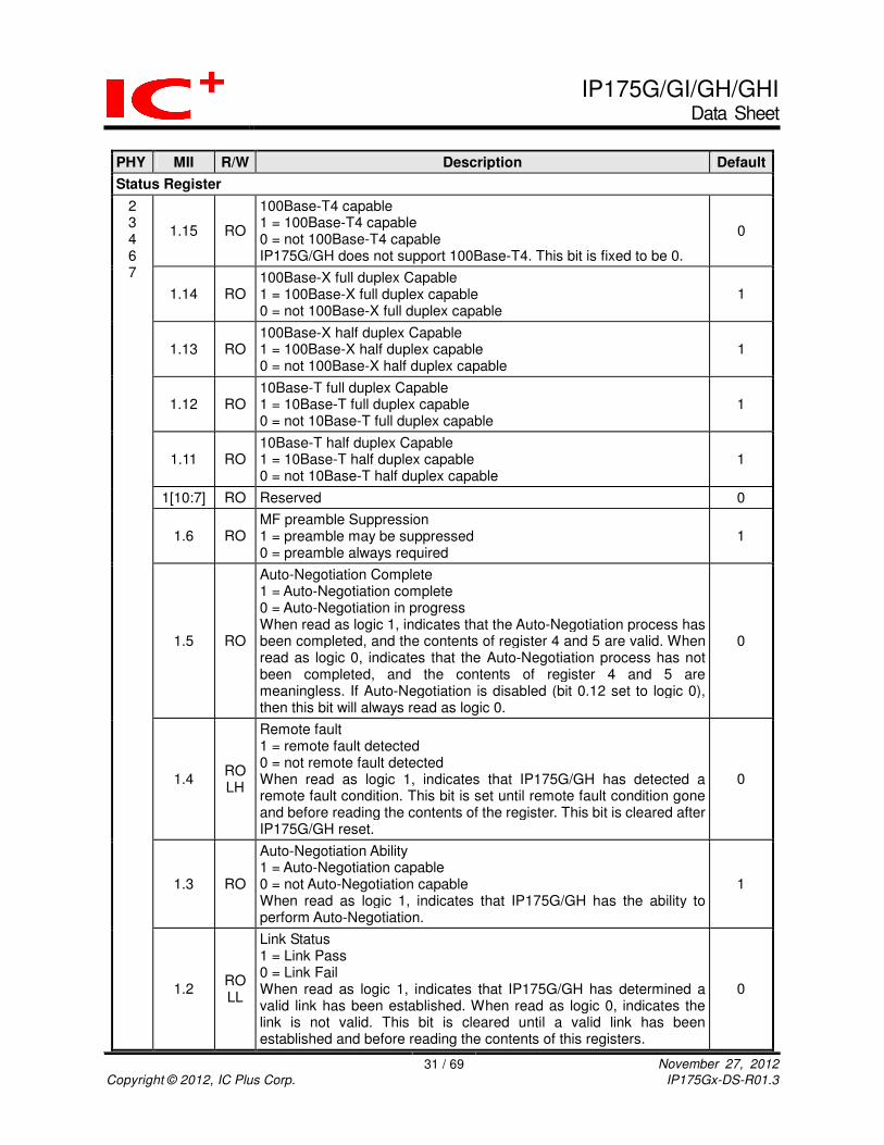
1.15 RO
100Base-T4 capable 1 = 100Base-T4 capable 0 = not 100Base-T4 capable IP175G/GH does not support 100Base-T4. This bit is fixed to be 0.
0
1.14 RO 100Base-X full duplex Capable 1 = 100Base-X full duplex capable 0 = not 100Base-X full duplex capable
1
1.13 RO 100Base-X half duplex Capable 1 = 100Base-X half duplex capable 0 = not 100Base-X half duplex capable
1
1.12 RO 10Base-T full duplex Capable 1 = 10Base-T full duplex capable 0 = not 10Base-T full duplex capable
1
1.11 RO 10Base-T half duplex Capable 1 = 10Base-T half duplex capable 0 = not 10Base-T half duplex capable
1
1[10:7] RO Reserved 0
1.6 RO MF preamble Suppression 1 = preamble may be suppressed 0 = preamble always required
1
1.5 RO
Auto-Negotiation Complete 1 = Auto-Negotiation complete 0 = Auto-Negotiation in progress When read as logic 1, indicates that the Auto-Negotiation process has been completed, and the contents of register 4 and 5 are valid. When read as logic 0, indicates that the Auto-Negotiation process has not been completed, and the contents of register 4 and 5 are meaningless. If Auto-Negotiation is disabled (bit 0.12 set to logic 0), then this bit will always read as logic 0.
0
1.4 RO LH
Remote fault 1 = remote fault detected 0 = not remote fault detected When read as logic 1, indicates that IP175G/GH has detected a remote fault condition. This bit is set until remote fault condition gone and before reading the contents of the register. This bit is cleared after IP175G/GH reset.
0
1.3 RO
Auto-Negotiation Ability 1 = Auto-Negotiation capable 0 = not Auto-Negotiation capable When read as logic 1, indicates that IP175G/GH has the ability to perform Auto-Negotiation.
1
2 3 4 6 7
1.2 RO LL
Link Status 1 = Link Pass 0 = Link Fail When read as logic 1, indicates that IP175G/GH has determined a valid link has been established. When read as logic 0, indicates the link is not valid. This bit is cleared until a valid link has been established and before reading the contents of this registers.
0

IP175G/GI/GH/GHI Data Sheet
32 / 69 November 27, 2012
Copyright © 2012, IC Plus Corp. IP175Gx-DS-R01.3
PHY MII R/W Description Default
Status Register
1.1
Jabber Detect 1 = jabber condition detected 0 = no jabber condition detected When read as logic 1, indicates that IP175G/GH has detected a jabber condition. This bit is always 0 for 100Mbps operation and is cleared after IP175G/GH reset. When the duration of TXEN exceeds the jabber timer (21ms), the transmission and loop back functions will be disabled and the COL is active. After TXEN goes low for more than 500 ms, the transmitter will be re-enabled.
0
1.0 RO
Extended capability 1 = Extended register capabilities 0 = No extended register capabilities IP175G/GH has extended register capabilities.
1
PHY MII R/W Description Default
PHY Identifier 1 Register
2 3 4 6 7
2 RO
IP175G/GH OUI (Organizationally Unique Identifier) ID, the MSB is 3rd
bit of IP175G/GH OUI ID, and the LSB is 18
th bit of IP175G/GH OUI
ID. IP175G/GH OUI is 0090C3. 16’h0243
PHY MII R/W Description Default
PHY Identifier 2 Register
3[15:10] RO PHY identifier IP175G/GH OUI ID, the MSB is 19
th bit of IP175G/GH OUI ID, and
LSB is 24th bit of IP175G/GH OUI ID.
6’h03
3[9:4] RO Manufacture’s Model Number IP175G/GH model number
6’h18
2 3 4 6 7
3[3:0] RO Revision Number IP175G/GH revision number
0

IP175G/GI/GH/GHI Data Sheet
33 / 69 November 27, 2012
Copyright © 2012, IC Plus Corp. IP175Gx-DS-R01.3
PHY MII R/W Description Default
Auto-Negotiation Advertisement Register
4.15 R/W 1 = Next pages are supported
0 = Next pages are not supported 1
4.14 RO Reserved by IEEE, write as 0, ignore on read 0
4.13 R/W Remote Fault 1 = Advertises that this port has detected a remote fault. 0 = There is no remote fault.
0
4.12 RO Reserved for future IEEE use, write as 0, ignore on read 0
4.11 RW
Asymmetric PAUSE
1 = Asymmetric flow control is supported
0 = Asymmetric flow control is not supported
1
4.10 RW
PAUSE
1 = Symmetric flow control is supported
0 = Symmetric flow control is not supported
1
4.9 RO 100BASE-T4 Not supported 0
4.8 R/W 100BASE-TX full duplex 1 = 100BASE-TX full duplex is supported 0 = 100BASE-TX full duplex is not supported
1
4.7 R/W 100BASE-TX 1 = 100BASE-TX is supported 0 = 100BASE-TX is not supported
1
4.6 R/W 10BASE-T full duplex 1 = 10BASE-T full duplex is supported 0 = 10BASE-T full duplex is not supported
1
4.5 R/W 10BASE-T 1 = 10BASE-T is supported 0 = 10BASE-T is not supported
1
2 3 4 6 7
4[4:0] RO Selector Field Use to identify the type of message being sent by Auto-Negotiation.
5’b00001
PHY MII R/W Description Default
Auto-Negotiation Link Partner Ability Register
5.15 RO Next Page 1 = Next Page ability is supported by link partner 0 = Next Page ability does not supported by link partner
0
5.14 RO Acknowledge 1 = Link partner has received the ability data word 0 = Not acknowledge
0
5.13 RO
Remote Fault 1 = Link partner indicates a remote fault 0 = No remote fault indicate by link partner If this bit is set to logic 1, then bit 1.4 (Remote fault) will set to logic 1.
0
2 3 4 6 7
5.12 RO Reserved by IEEE for future use, write as 0, and read as 0. 0

IP175G/GI/GH/GHI Data Sheet
34 / 69 November 27, 2012
Copyright © 2012, IC Plus Corp. IP175Gx-DS-R01.3
PHY MII R/W Description Default
5.11 RO
Asymmetric PAUSE 1 = Link partner support Asymmetric PAUSE 0 = Link partner does not support Asymmetric PAUSE When local or link partner is Auto-negotiation disabled, this bit is read as 1. The pause resolution is determined by MII Reg4.[11:10].
0
5.10 RO
PAUSE 1 = Link partner support Symmetric PAUSE 0 = Link partner does not support Symmetric PAUSE When local or link partner is Auto-negotiation disabled, this bit is read as 1. The pause resolution is determined by MII Reg4.[11:10].
0
5.9 RO 100BASE-T4 1 = Link partner support 100BASE-T4 0 = Link partner does not support 100BASE-T4
0
5.8 RO 100BASE-TX full duplex 1 = Link partner support 100BASE-TX full duplex 0 = Link partner does not support 100BASE-TX full duplex
0
5.7 RO 100BASE-TX 1 = Link partner support 100BASE-TX 0 = Link partner does not support 100BASE-TX
0
5.6 RO 10BASE-T full duplex 1 = Link partner support 10BASE-T full duplex 0 = Link partner does not support 10BASE-T full duplex
0
5.5 RO
10BASE-T 1 = Link partner support 10BASE-T 0 = Link partner does not support 10BASE-T When AN is disabled, this bit is set if register 0.13=0
0
5[4:0] RO Selector Field Protocol selector of the link partner
5’b00000
PHY MII R/W Description Default
Auto-Negotiation Expansion Register
6[15:5] RO Reserved 0
6.4 RO 1 = a fault has been detected via parallel detection function. 0 = a fault has not been detected via parallel detection function.
0
6.3 RO 1 = Link partner is next page able. 0 = Link partner is not next page able.
0
6.2 RO 1 = IP175G/GH next page able. 0 = IP175G/GH is not next page able.
0
6.1 RO/ LH
1 = A new page has been received. 0 = A new page has not been received.
0
2 3 4 6 7
6.0 RO
If AN is enabled, this bit means: 1 = Link partner is Auto-Negotiation able. 0 = Link partner is not Auto-Negotiation able. In 100FX or AN disabled, then this bit is always equal to 0.
0 (AN)
(100FX)
IP175G/GI/GH/GHI Data Sheet
35 / 69 November 27, 2012
Copyright © 2012, IC Plus Corp. IP175Gx-DS-R01.3
PHY MII R/W Description Default
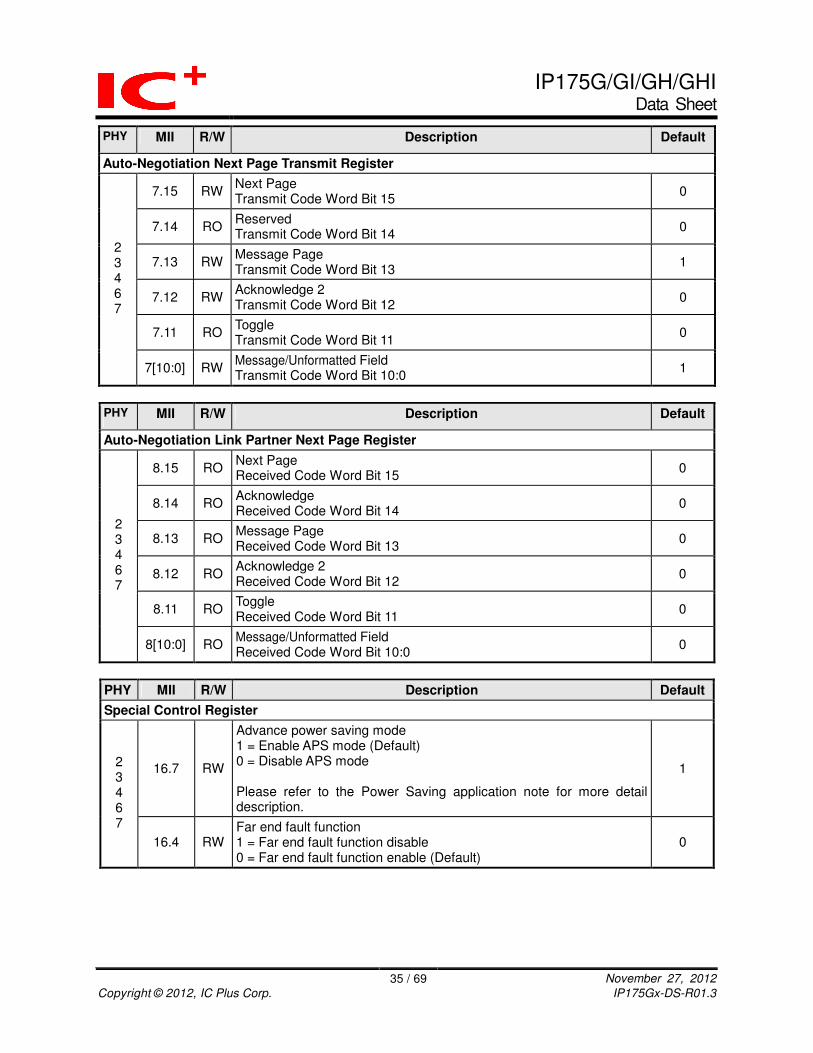
Auto-Negotiation Next Page Transmit Register
7.15 RW Next Page Transmit Code Word Bit 15
0
7.14 RO Reserved Transmit Code Word Bit 14
0
7.13 RW Message Page Transmit Code Word Bit 13
1
7.12 RW Acknowledge 2 Transmit Code Word Bit 12
0
7.11 RO Toggle Transmit Code Word Bit 11
0
2 3 4 6 7
7[10:0] RW Message/Unformatted Field Transmit Code Word Bit 10:0
1
PHY MII R/W Description Default
Auto-Negotiation Link Partner Next Page Register
8.15 RO Next Page Received Code Word Bit 15
0
8.14 RO Acknowledge Received Code Word Bit 14
0
8.13 RO Message Page Received Code Word Bit 13
0
8.12 RO Acknowledge 2 Received Code Word Bit 12
0
8.11 RO Toggle Received Code Word Bit 11
0
2 3 4 6 7
8[10:0] RO Message/Unformatted Field Received Code Word Bit 10:0
0
PHY MII R/W Description Default
Special Control Register
16.7 RW
Advance power saving mode 1 = Enable APS mode (Default) 0 = Disable APS mode Please refer to the Power Saving application note for more detail description.
1 2 3 4 6 7
16.4 RW Far end fault function 1 = Far end fault function disable 0 = Far end fault function enable (Default)
0

IP175G/GI/GH/GHI Data Sheet
36 / 69 November 27, 2012
Copyright © 2012, IC Plus Corp. IP175Gx-DS-R01.3
PHY MII R/W Description Default
Special Status Register
18.14 RO Linkup 1 = linkup 0 = unlink
0
18.11 RO Speed Mode 1 = 100 Mbps 0 = 10 Mbps
0
2 3 4 6 7
18.10 RO Duplex Mode 1 = Full Duplex 0 = Half Duplex
0
The other Registers are reserved registers. User is inhibited to access to these registers. It may introduce abnormal function to write these registers.

IP175G/GI/GH/GHI Data Sheet
37 / 69 November 27, 2012
Copyright © 2012, IC Plus Corp. IP175Gx-DS-R01.3
6.2 MMD Control Register
Table 8 MMD Control Register table
PHY MII R/W Description Default
MMD Access Control Register
13[15:14] R/W
Function 00 = address 01 = data, no post increment 10 = data, post increment on reads and writes 11 = data, post increment on writes only
0
13[13:5] R/W Reserved Write as 0, ignore on read
0
2 3 4 6 7
13[4:0] R/W DEVAD Device Address
0
PHY MII R/W Description Default
MMD Access Address Data Register
2 3 4 6 7
14[15:0] R/W
Address Data If 13.15:14 = 00, MMD DEVAD’s address register. Otherwise, MMD DEVAD’s data register as indicated by the contents of its address register
0
Example 1, Read 2.3.20 (Read Data from MMD register 3.20 of PHY address 2):
1. Write 2.13 = 0x0003 //MMD DEVAD 3 2. Write 2.14 = 0x0014 //MMD Address 20 3. Write 2.13 = 0x4003 //MMD Data command for MMD DEVAD 3 4. Read 2.14 //Read MMD Data from 2.3.20
Example 2, Write 3.7.60 = 0x3210 (Write 0x3210 Data to MMD register 7.60 of PHY address 3):
1. Write 3.13 = 0x0007 //MMD DEVAD 7 2. Write 3.14 = 0x003C //MMD Address 60 3. Write 3.13 = 0x4007 //MMD Data command for MMD DEVAD 7 4. Write 3.14 = 0x3210 //Write MMD Data 0x3210 to 3.7.60
6.3 MMD Data Register
Table 9 MMD Data Register table
PHY MII R/W Description Default
PCS control 1 Register
3.0[15:11] RO Reserved Ignore when read
0
3.0.10 R/W Clock stop enable 1 = IP175G/GH may stop xMII Rx clock during LPI 0 = Clock not stoppable
0
2 3 4 6 7
3.0[9:0] RO Reserved Ignore when read
0
IP175G/GI/GH/GHI Data Sheet
38 / 69 November 27, 2012
Copyright © 2012, IC Plus Corp. IP175Gx-DS-R01.3
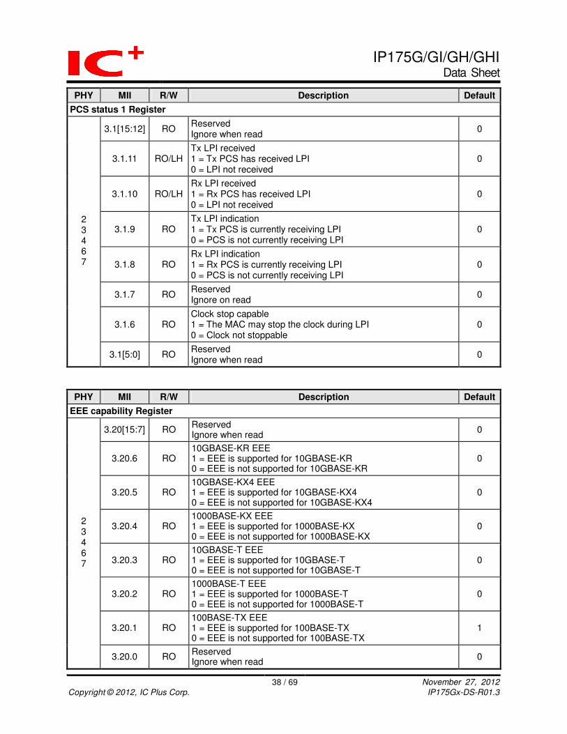
PHY MII R/W Description Default
PCS status 1 Register
3.1[15:12] RO Reserved Ignore when read
0
3.1.11 RO/LH Tx LPI received 1 = Tx PCS has received LPI 0 = LPI not received
0
3.1.10 RO/LH Rx LPI received 1 = Rx PCS has received LPI 0 = LPI not received
0
3.1.9 RO Tx LPI indication 1 = Tx PCS is currently receiving LPI 0 = PCS is not currently receiving LPI
0
3.1.8 RO Rx LPI indication 1 = Rx PCS is currently receiving LPI 0 = PCS is not currently receiving LPI
0
3.1.7 RO Reserved Ignore on read
0
3.1.6 RO Clock stop capable 1 = The MAC may stop the clock during LPI 0 = Clock not stoppable
0
2 3 4 6 7
3.1[5:0] RO Reserved Ignore when read
0
PHY MII R/W Description Default
EEE capability Register
3.20[15:7] RO Reserved Ignore when read
0
3.20.6 RO 10GBASE-KR EEE 1 = EEE is supported for 10GBASE-KR 0 = EEE is not supported for 10GBASE-KR
0
3.20.5 RO 10GBASE-KX4 EEE 1 = EEE is supported for 10GBASE-KX4 0 = EEE is not supported for 10GBASE-KX4
0
3.20.4 RO 1000BASE-KX EEE 1 = EEE is supported for 1000BASE-KX 0 = EEE is not supported for 1000BASE-KX
0
3.20.3 RO 10GBASE-T EEE 1 = EEE is supported for 10GBASE-T 0 = EEE is not supported for 10GBASE-T
0
3.20.2 RO 1000BASE-T EEE 1 = EEE is supported for 1000BASE-T 0 = EEE is not supported for 1000BASE-T
0
3.20.1 RO 100BASE-TX EEE 1 = EEE is supported for 100BASE-TX 0 = EEE is not supported for 100BASE-TX
1
2 3 4 6 7
3.20.0 RO Reserved Ignore when read
0
IP175G/GI/GH/GHI Data Sheet
39 / 69 November 27, 2012
Copyright © 2012, IC Plus Corp. IP175Gx-DS-R01.3
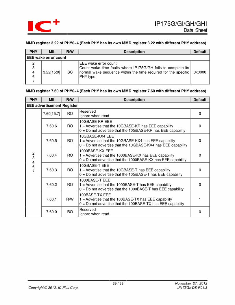
MMD register 3.22 of PHY0~4 (Each PHY has its own MMD register 3.22 with different PHY address)
PHY MII R/W Description Default
EEE wake error count
2 3 4 6 7
3.22[15:0] SC
EEE wake error count Count wake time faults where IP175G/GH fails to complete its normal wake sequence within the time required for the specific PHY type.
0x0000
MMD register 7.60 of PHY0~4 (Each PHY has its own MMD register 7.60 with different PHY address)
PHY MII R/W Description Default
EEE advertisement Register
7.60[15:7] RO Reserved Ignore when read
0
7.60.6 RO 10GBASE-KR EEE 1 = Advertise that the 10GBASE-KR has EEE capability 0 = Do not advertise that the 10GBASE-KR has EEE capability
0
7.60.5 RO 10GBASE-KX4 EEE 1 = Advertise that the 10GBASE-KX4 has EEE capability 0 = Do not advertise that the 10GBASE-KX4 has EEE capability
0
7.60.4 RO 1000BASE-KX EEE 1 = Advertise that the 1000BASE-KX has EEE capability 0 = Do not advertise that the 1000BASE-KX has EEE capability
0
7.60.3 RO 10GBASE-T EEE 1 = Advertise that the 10GBASE-T has EEE capability 0 = Do not advertise that the 10GBASE-T has EEE capability
0
7.60.2 RO 1000BASE-T EEE 1 = Advertise that the 1000BASE-T has EEE capability 0 = Do not advertise that the 1000BASE-T has EEE capability
0
7.60.1 R/W 100BASE-TX EEE 1 = Advertise that the 100BASE-TX has EEE capability 0 = Do not advertise that the 100BASE-TX has EEE capability
1
2 3 4 6 7
7.60.0 RO Reserved Ignore when read
0

IP175G/GI/GH/GHI Data Sheet
40 / 69 November 27, 2012
Copyright © 2012, IC Plus Corp. IP175Gx-DS-R01.3
MMD register 7.61 of PHY0~4 (Each PHY has its own MMD register 7.61 with different PHY address)
PHY MII R/W Description Default
EEE link partner ability
7.61[15:7] RO Reserved Ignore when read
0
7.61.6 RO 10GBASE-KR EEE 1 = Link partner is advertising EEE capability for 10GBASE-KR 0 = Link partner is not advertising EEE capability for 10GBASE-KR
0
7.61.5 RO 10GBASE-KX4 EEE 1 = Link partner is advertising EEE capability for 10GBASE-KX4 0 = Link partner is not advertising EEE capability for 10GBASE-KX4
0
7.61.4 RO 1000BASE-KX EEE 1 = Link partner is advertising EEE capability for 1000BASE-KX 0 = Link partner is not advertising EEE capability for 1000BASE-KX
0
7.61.3 RO 10GBASE-T EEE 1 = Link partner is advertising EEE capability for 10GBASE-T 0 = Link partner is not advertising EEE capability for 10GBASE-T
0
7.61.2 RO 1000BASE-T EEE 1 = Link partner is advertising EEE capability for 1000BASE-T 0 = Link partner is not advertising EEE capability for 1000BASE-T
0
7.61.1 RO 100BASE-TX EEE 1 = Link partner is advertising EEE capability for 100BASE-TX 0 = Link partner is not advertising EEE capability for 100BASE-TX
0
2 3 4 6 7
7.61.0 RO Reserved Ignore when read
0
The other Registers are reserved registers. User is inhibited to access to these registers. It may introduce abnormal function to write these registers.
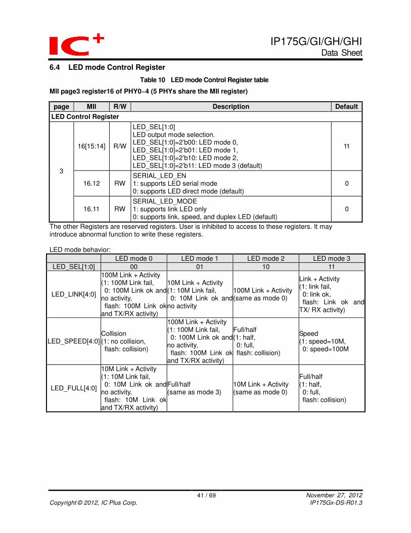
IP175G/GI/GH/GHI Data Sheet
41 / 69 November 27, 2012
Copyright © 2012, IC Plus Corp. IP175Gx-DS-R01.3
6.4 LED mode Control Register
Table 10 LED mode Control Register table
MII page3 register16 of PHY0~4 (5 PHYs share the MII register)
page MII R/W Description Default
LED Control Register
16[15:14] R/W
LED_SEL[1:0] LED output mode selection. LED_SEL[1:0]=2’b00: LED mode 0, LED_SEL[1:0]=2’b01: LED mode 1, LED_SEL[1:0]=2’b10: LED mode 2, LED_SEL[1:0]=2’b11: LED mode 3 (default)
11
16.12 RW SERIAL_LED_EN 1: supports LED serial mode 0: supports LED direct mode (default)
0
3
16.11 RW SERIAL_LED_MODE 1: supports link LED only 0: supports link, speed, and duplex LED (default)
0
The other Registers are reserved registers. User is inhibited to access to these registers. It may introduce abnormal function to write these registers. LED mode behavior:
LED mode 0 LED mode 1 LED mode 2 LED mode 3
LED_SEL[1:0] 00 01 10 11
LED_LINK[4:0]
100M Link + Activity (1: 100M Link fail, 0: 100M Link ok and no activity, flash: 100M Link ok and TX/RX activity)
10M Link + Activity (1: 10M Link fail, 0: 10M Link ok and no activity
100M Link + Activity (same as mode 0)
Link + Activity (1: link fail, 0: link ok, flash: Link ok and TX/ RX activity)
LED_SPEED[4:0] Collision (1: no collision, flash: collision)
100M Link + Activity (1: 100M Link fail, 0: 100M Link ok and no activity, flash: 100M Link ok and TX/RX activity)
Full/half (1: half, 0: full, flash: collision)
Speed (1: speed=10M, 0: speed=100M
LED_FULL[4:0]
10M Link + Activity (1: 10M Link fail, 0: 10M Link ok and no activity, flash: 10M Link ok
and TX/RX activity)
Full/half (same as mode 3)
10M Link + Activity (same as mode 0)
Full/half (1: half, 0: full, flash: collision)

IP175G/GI/GH/GHI Data Sheet
42 / 69 November 27, 2012
Copyright © 2012, IC Plus Corp. IP175Gx-DS-R01.3
6.5 Register Page mode Control Register
Table 11 Register Page mode Control Register table
MII register 20 of PHY0~4 (Each PHY has its own MII register 20 with different PHY address)
PHY MII R/W Description Default
Page Control Register
2 3 4 6 7
20[4:0] RW Reg16~31_Page_Sel[4:0] 00000
The other Registers are reserved registers. User is inhibited to access to these registers. It may introduce abnormal function to write these registers. 6.6 WOL+ Control Register
Table 12 WOL+ Control Register table
page MII R/W Description Default
PHY WOL+ Control Register
16.[15] RW
WOL+ Interrupt Enable Set high to enable WOL+ interrupt 1=Enable 0=Disable
0
16.[14] RW
WOL+ Level Trigger This bit is used to select the output mode of WOL+ interrupt. 1=Level trigger (Low goes high or high goes low when WOL+ interrupt) 0=Edge trigger (Positive pulse or negative pulse when WOL+ interrupt)
1
16.[13] RW
WOL+ Positive Trigger This bit is used to select the polarity of WOL+ interrupt. 1=Low goes high or positive pulse 0=High goes low or negative pulse
0
16.[12] RW
Sense Link Change Set high to enable WOL+ interrupt when link change is sensing. 1=Enable 0=Disable
1
16.[11] RW
Sense Magic Packet Set high to enable WOL+ interrupt when magic packet is receiving. 1=Enable 0=Disable
1
4
16.[10] RW
Sense Any Packet Set high to enable WOL+ interrupt when any packet is receiving. 1=Enable 0=Disable
1
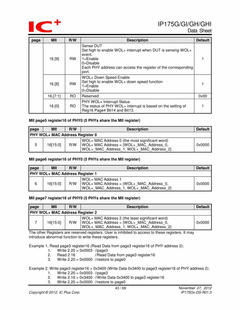
IP175G/GI/GH/GHI Data Sheet
43 / 69 November 27, 2012
Copyright © 2012, IC Plus Corp. IP175Gx-DS-R01.3
page MII R/W Description Default
16.[9] RW
Sense DUT Set high to enable WOL+ interrupt when DUT is sensing WOL+ event. 1=Enable 0=Disable Each PHY address can access the register of the corresponding port.
1
16.[8] RW
WOL+ Down Speed Enable Set high to enable WOL+ down speed function 1=Enable 0=Disable
1
16.[7:1] RO Reserved 0x00
16.[0] RO PHY WOL+ Interrupt Status The status of PHY WOL+ interrupt is based on the setting of Reg16 Page4 Bit14 and Bit13.
1
MII page5 register16 of PHY0 (5 PHYs share the MII register)
page MII R/W Description Default
PHY WOL+ MAC Address Register 0
5 16[15:0] R/W WOL+ MAC Address 0 (the most significant word) WOL+ MAC Address = {WOL+_MAC_Address_0, WOL+_MAC_Address_1, WOL+_MAC_Address_2}
0x0000
MII page6 register16 of PHY0 (5 PHYs share the MII register)
page MII R/W Description Default
PHY WOL+ MAC Address Register 1
6 16[15:0] R/W WOL+ MAC Address 1 WOL+ MAC Address = {WOL+_MAC_Address_0, WOL+_MAC_Address_1, WOL+_MAC_Address_2}
0x0000
MII page7 register16 of PHY0 (5 PHYs share the MII register)
page MII R/W Description Default
PHY WOL+ MAC Address Register 2
7 16[15:0] R/W WOL+ MAC Address 2 (the least significant word) WOL+ MAC Address = {WOL+_MAC_Address_0, WOL+_MAC_Address_1, WOL+_MAC_Address_2}
0x0000
The other Registers are reserved registers. User is inhibited to access to these registers. It may introduce abnormal function to write these registers. Example 1, Read page3 register16 (Read Data from page3 register16 of PHY address 2):
1. Write 2.20 = 0x0003 //page3 2. Read 2.16 //Read Data from page3 register16 3. Write 2.20 = 0x0000 //restore to page0
Example 2, Write page3 register16 = 0x3400 (Write Data 0x3400 to page3 register16 of PHY address 2):
1. Write 2.20 = 0x0003 //page3 2. Write 2.16 = 0x3400 //Write Data 0x3400 to page3 register16 3. Write 2.20 = 0x0000 //restore to page0

IP175G/GI/GH/GHI Data Sheet
44 / 69 November 27, 2012
Copyright © 2012, IC Plus Corp. IP175Gx-DS-R01.3
6.7 Switch control registers (I)
Table 13 Switch control registers (I) table
PHY MII ROM R/W Description Default
EEPROM enable register / Software reset register
20 -- 1, 0
EEPROM enable register This register should be filled with 55AA in EERPOM register 0 and 1. IP175G/GH will examine the specified pattern to confirm if there is a valid EEPROM. The initial setting is updated with the content of EEPROM only if the specified pattern 55AA is found.
20 0 R/W Software reset register MII register 0 is software reset register. User can reset IP175G/GH by writing 55AA to this register.
20 0[15] R
BFLL_FULL, free buffer is full 1: full, 0: not full This bit is for debug only.
20 0[13] R
Empty, all output queue is empty 1: empty 0: not empty This bit is for debug only.
20 0[12:4] Reserved
20 0[3] R PAD_RESET
20 0[2] R EE_RESET1
20 0[1] R SOFT_RESET
20 0[0] R EE_RESET
20 1[15] R/W
PRIORITY_RATE 1: 8 packets 0: 16 packets Output Queue Scheduling: high priority packet rate
1’b0
20 1[12] R/W REDUCE_IPG This function reduce the IPG by random from 0 ~ 20 PPM. 1: enable, 0:disable
1'b1
20 1[11] R/W Drop16 1: enable, 0:disable
1’b0
20 1[9] R/W MOD_CARRIER_ALGORITHM Modified carrier based collision algorithm 1: enable, 0:disable
1’b0
20 1[8] R/W BK_EN, Backpressure enable 1: enable, 0: disable
1'b1
20 1[7] R/W
BP_KIND, Backpressure type selection It is valid only if BK_EN is set to 1’b1. 0: carrier base backpressure 1: reserved
1’b0

IP175G/GI/GH/GHI Data Sheet
45 / 69 November 27, 2012
Copyright © 2012, IC Plus Corp. IP175Gx-DS-R01.3
PHY MII ROM R/W Description Default
20 1[6] R/W
BF_STM_EN, Broadcast storm enable 1: enable IP175G/GH drops the incoming packet if the number of broadcast packet in queue is over the threshold. 0: disable
P(0)
AGING. Aging time of address table selection An address tag in hashing table will be removed if this function is turned on and its aging timer expires.
Aging time note
00 no aging
01 30s
10 300s default
20 1[3:2] R/W
11 reserved
2’b10
20 1[1] R/W
MODBCK. Turn on modified back off algorithm The maximum back off period is limited to 8-slot time if this function is turned on. 1: turn on, 0: turn off
1'b0
20 1[0] 2[0] R/W LEARN_DIS_PAUSE 0: Enable to learn the SMAC of the received PAUSE frame. 1: Disable.
1’b0
6.8 Test mode control registers
Table 14 Test mode control registers table
PHY MII R/W Description Default
Test mode control registers
20 2[15:10] R/W TMODE_SEL. Test mode selection This function is for testing only. The default value must be adopted for normal operation.
6’h00
20 2[8] Reserved
20 2[7] R/W
INPUT_FILTER Packet is filtered in input port. 1: perform input filtering when queue full 0: no operation (default)
0
20 2[6:5] R/W
HASH_MODE MAC address table hashing mode 00: direct + CRC mapping (default) 11: direct mapping
2’b00
20 2[4:1] Reserved

IP175G/GI/GH/GHI Data Sheet
46 / 69 November 27, 2012
Copyright © 2012, IC Plus Corp. IP175Gx-DS-R01.3
6.9 Port mirroring control registers
Table 15 Port mirroring control registers table
PHY MII R/W Description Default
3[15] R/W PORT_MIRROR_EN 1’b0
20 3[14:13] R/W
PORT_MIRROR_MODE Select a mirror mode to monitor 00: mirror RX (default) 01: mirror TX 10: mirror RX and TX 11: mirror RX or TX
2’b00
3[12:8] Reserved
3[7:0] R/W
SEL_RX_PORT_MIRROR Select the source (receive) port to be mirrored 0000_0010: port 0 Note 1 0000_0011: port 1 0000_0100: port 2 0000_0110: port 3 0001_0111: port 4
8’h01
4[15:13] R/W
SEL_MIRROR_PORT Select a mirror port to monitor any other port 010: port 0 Note 1 011: port 1 100: port 2 110: port 3 111: port 4 (default)
3’b111
4[12:8] Reserved
4[7:0] R/W
SEL_TX_PORT_MIRROR Select the destination (transmit) port to be mirrored 0000_0010: port 0 Note 1 0000_0011: port 1 0000_0100: port 2 0000_0110: port 3 0001_0111: port 4
8’h01
Note 1 : Port mapping refer Figure 2 Application Diagram 6.10 Debug Register
Table 16 Debug Register table
PHY MII R/W Description Default
20 5[15:8] R/W RESERVED 16’h0
20 5[7:0] RO (SC)
CRC_COUNTER 8’h00
20 6[15:8] R/W (SC)
PAUSE_TRIGGER 8’h00
20 6[7:0] RO (SC)
PAUSE_FLAG 8’h0
20 7[15] R/W THR_SETTING 1’b0

IP175G/GI/GH/GHI Data Sheet
47 / 69 November 27, 2012
Copyright © 2012, IC Plus Corp. IP175Gx-DS-R01.3
PHY MII R/W Description Default
20 7[14] R/W (SC)
READ_THR 1’b0
20 7[13] R/W WAIT_BACKOFF 1’b0
20 7[12:8] RESERVED
20 7[7:0] R/W UNIT_DEFAULT_THRESHOLD 8’d12
20 8[15:8] R/W SHARE_HIGH_THRESHOLD
20 8[7:0] R/W SHARE_LOW_THRESHOLD
20 9[15:8] R/W PKT_HIGH_THRESHOLD 8’d96
20 9[7:0] R/W PKT_LOW_THRESHOLD 8’d80
20 10[15:8] R/W UNIT_HIGH_THRESHOLD
20 10[7:0] R/W UNIT_LOW_THRESHOLD
20 11[15] R/W MON_EN 1’b0
20 11[14:9] RESERVED
20 11[8:0] RO (SC)
UNIT_LOW_NUM 9’d224
20 12[15:9] RESERVED
20 12[8:0] RO (SC)
SHARE_HIGH_NUM 9’d224
6.11 Fiber duplex setting registers
Table 17 Fiber duplex setting registers table
PHY MII R/W Description Default
20 13[15:14] R/W
FIBER_DUPLEX Fiber duplex setting for each port. 1: fiber port is full-duplex 0: fiber port is half_duplex bit[14]: port 4 duplex ability setting
2’b11
20 13.[13] R/W BUF_AGING_EN 1’b0
20 13.[12] R/W SRC_BLK_PROTECT 1’b1
20 13[11:8] Reserved

IP175G/GI/GH/GHI Data Sheet
48 / 69 November 27, 2012
Copyright © 2012, IC Plus Corp. IP175Gx-DS-R01.3
6.12 Backpressure setting registers
PHY MII R/W Description Default
20 13[7:0] R/W
PORT_BACKPRESSURE_EN Backpressure ability setting at half-duplex mode for each port. To ensure this function works correctly, BK_EN (backpressure enable, reg 20.1[8]) should set to logic zero first. 1: enable backpressure ability 0: disable bit[7]: port 4 enable backpressure ability Note 1 bit[6]: port 3 enable backpressure ability bit[4]: port 2 enable backpressure ability bit[3]: port 1 enable backpressure ability bit[2]: port 0 enable backpressure ability
8’h00
6.13 TCP/UDP port priority registers
PHY MII R/W Description Default
20 14[15:8] R/W
LPP_AGING_EN TCP/UDP logical port priority aging enable 0: disable TCP/UDP logical port priority aging function 1: enable TCP/UDP logical port priority aging function When this function active, once receive a IP frame with TCP/UDP protocol and the logical port number is the pre-defined port number, the ingress port will treat as a port based high priority port for 300 seconds. After the internal timer expired, the ingress port will change back to previous behavior. bit[15]: port 4 logical port priority aging enable Note 1 bit[14]: port 3 logical port priority aging enable bit[12]: port 2 logical port priority aging enable bit[11]: port 1 logical port priority aging enable bit[10]: port 0 logical port priority aging enable
8’h00
20 14[7:6] Reserved
20 14[5:4] R/W
USERDEF_RANGE_EN User defined logic port range enable. bit[1]: user define range 1 register enable bit[0]: user define range 0 register enable
2’b11
20 14[3:0] R/W
PREDEF_PORT_EN Pre-defined logic port number enable. bit[3]: logic port set 3 enable, port 6000 bit[2]: logic port set 2 enable, port 3389 bit[1]: logic port set 1 enable, port 443 bit[0]: logic port set 0 enable, port 22
4’hF
20 15 R/W USERDEF_RANGE0_HIGH User defined logic port range 0 high limit
16’d23
20 16 R/W USERDEF_RANGE0_LOW User defined logic port range 0 low limit
16’d23
20 17 R/W USERDEF_RANGE1_HIGH User defined logic port range 1 high limit
16’d 5800
20 18 R/W USERDEF_RANGE1_LOW User defined logic port range 1 low limit
16’d 5800
Note 1 : Port mapping refer Figure 2 Application Diagram

IP175G/GI/GH/GHI Data Sheet
49 / 69 November 27, 2012
Copyright © 2012, IC Plus Corp. IP175Gx-DS-R01.3
6.14 Test mode
PHY MII R/W Description Default
20 19[15] R/W FAST_MODE 1’b0
20 19[11:2] R/W TEST_LATIN (only for PHY test mode) 10’h000
20 19[1:0] R/W
TEST_SEL 0x0: normal mode 0x1: switch test mode 0x2: phy test mode
2’b00
6.15 CoS control registers – port 0
PHY MII R/W Description Default
2[10] R/W
Port 0 Class of service enable 1: enable, 0: disabled (default) Packets with high priority tag from port 0 are handled as high priority packets.
1’b0
21
2[9] R/W Port 0 set to be high priority port 1: enable, 0: disabled (default) Packets received from port 0 are handled as high priority packets.
1’b0
6.16 CoS control registers – port 1
PHY MII R/W Description Default
3[10] R/W
Port 1 Class of service enable 1: enable, 0: disabled (default) Packets with high priority tag from port 1 are handled as high priority packets.
1’b0
21
3[9] R/W Port 1 set to be high priority port 1: enable, 0: disabled (default) Packets received from port 1 are handled as high priority packets.
1’b0
6.17 CoS control registers – port 2
PHY MII R/W Description Default
4[10] R/W
Port 2 Class of service enable 1: enable, 0: disabled (default) Packets with high priority tag from port 2 are handled as high priority packets.
1’b0
21
4[9]
R/W Port 2 set to be high priority port 1: enable, 0: disabled (default) Packets received from port 2 are handled as high priority packets.
1’b0

IP175G/GI/GH/GHI Data Sheet
50 / 69 November 27, 2012
Copyright © 2012, IC Plus Corp. IP175Gx-DS-R01.3
6.18 CoS control registers – port 3
PHY MII R/W Description Default
6[10] R/W
Port 3 Class of service enable 1: enable, 0: disabled (default) Packets with high priority tag from port 3 are handled as high priority packets.
1’b0
21
6[9] R/W Port 3 set to be high priority port 1: enable, 0: disabled (default) Packets received from port 3 are handled as high priority packets.
1’b0
6.19 CoS control registers – port 4
PHY MII R/W Description Default
CoS and port base VLAN register 4
7[10] R/W
Port 4 Class of service enable 1: enable, 0: disabled (default) Packets with high priority tag from port 4 are handled as high priority packets.
1’b0
21
7[9] R/W Port 4 set to be high priority port 1: enable, 0: disabled (default) Packets received from port 4 are handled as high priority packets.
1’b0
6.20 Switch control registers (IV)
PHY MII R/W Description Default
9[15:14] R/W
BF_STM_THR_SEL[1:0]. Broadcast storm threshold selection 00: 2 packets/10ms for 100Mbps port, or 2 packets/100ms for
10Mbps port, 01: 6 packets/10ms for 100Mbps port, or 6 packets/100ms for
10Mbps port, 10: 14 packets/10ms for 100Mbps port, or 14 packets/100ms for
10Mbps port, 11: 30 packets/10ms for 100Mbps port, or 30 packets/100ms for
10Mbps port
2’b00
9[13:12] R/W
SHARE_FULL_THR_SEL[1;0]. Share buffer threshold selection 00: 160 units 01: 180 units 10: 140 units 11: 120 units
2’b00
21
9[11:10] R/W
UNIT_DEFAULT_THR_SEL[1:0]. Output Queue minimum threshold selection 00: 40 units 01: 32 units 10: 48 units 11: 56 units
2’b00

IP175G/GI/GH/GHI Data Sheet
51 / 69 November 27, 2012
Copyright © 2012, IC Plus Corp. IP175Gx-DS-R01.3
PHY MII R/W Description Default
9[9:8] R/W UNIT_LOW_THR_SEL 2’b00
9[7:6] R/W
UNIT_HIGH_THR_SEL[1;0]. Output Queue Flow control ON threshold selection If share buffer is over share buffer full threshold, Output Queue Flow control ON threshold will be dynamic changed to 28. Others, 00: 50 units 01: 70 units 10: 90 units 11: 110 units
2’b00
9[5] Reserved
9[4] R/W
PREDROP_EN 1: Drop an incoming broadcast packet if any port is congested. 0: forward an incoming broadcast packet to un-congested ports instead of congested ports.
1’b0
9[3:2] R/W
PKT_LOW_THR_SEL[1:0]. Packet low water mark threshold selection 00: 40 units 01: 30 units 10: 20 units 11: 10 units
2’b00
9[1:0] R/W
PKT_HIGH_THR_SEL[1:0]. Packet high water mark threshold selection 00: 50 units 01: 40 units 10: 30 units 11: 20 units
2’b00
21 10[15] RESERVED
21 10[14:12] R/W
DRIVER[2:0] Pad Drive Current 000: 0 mA 001: 1.5 mA 010: 4.6 mA (default) 011: 9.9 mA 100: 9.9 mA 101: 9.9 mA 110: 15.1 mA 111: 18.4 mA
3’b 010
21 10[11] R/W BF_STM_EN_QM 1’b0
21 10[10] R/W HP_DIS_FLOW_EN Disable flow control when recived high priority packet
1’b0
21 10[9] R/W TWOPART 1’b1
21 10[8] R/W ALLPASS All packet forwarded include CRC packet.
1’b0
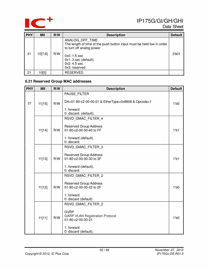
IP175G/GI/GH/GHI Data Sheet
52 / 69 November 27, 2012
Copyright © 2012, IC Plus Corp. IP175Gx-DS-R01.3
PHY MII R/W Description Default
21 10[7:6] R/W
ANALOG_OFF_TIME The length of time of the push button input must be held low in order to turn off analog power 0x0: 1.5 sec 0x1: 3 sec (default) 0x2: 4.5 sec 0x3: reserved
2’b01
21 10[5] RESERVED
6.21 Reserved Group MAC addresses
PHY MII R/W Description Default
11[15] R/W
PAUSE_FILTER DA=01-80-c2-00-00-01 & EtherType=0x8808 & Opcode=1 1: forward 0: discard. (default),
1’b0
11[14] R/W
RSVD_GMAC_FILTER_4 Reserved Group Address 01-80-c2-00-00-40 to FF 1: forward (default), 0: discard.
1’b1
11[13] R/W
RSVD_GMAC_FILTER_3 Reserved Group Address 01-80-c2-00-00-30 to 3F 1: forward (default), 0: discard.
1’b1
11[12] R/W
RSVD_GMAC_FILTER_2 Reserved Group Address 01-80-c2-00-00-22 to 2F 1: forward 0: discard (default)
1’b0
21
11[11] R/W
RSVD_GMAC_FILTER_2 GVRP GARP VLAN Registration Protocol 01-80-c2-00-00-21 1: forward 0: discard (default),
1’b0
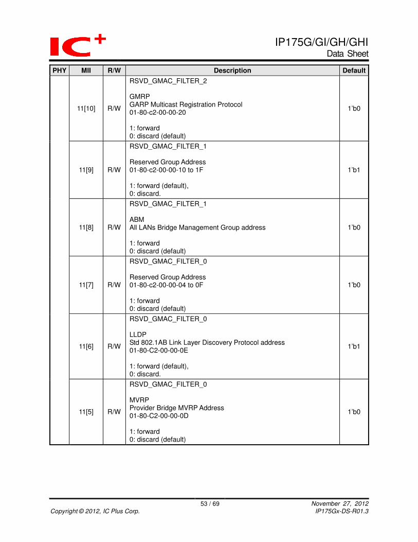
IP175G/GI/GH/GHI Data Sheet
53 / 69 November 27, 2012
Copyright © 2012, IC Plus Corp. IP175Gx-DS-R01.3
PHY MII R/W Description Default
11[10] R/W
RSVD_GMAC_FILTER_2 GMRP GARP Multicast Registration Protocol 01-80-c2-00-00-20 1: forward 0: discard (default)
1’b0
11[9] R/W
RSVD_GMAC_FILTER_1 Reserved Group Address 01-80-c2-00-00-10 to 1F 1: forward (default), 0: discard.
1’b1
11[8] R/W
RSVD_GMAC_FILTER_1 ABM All LANs Bridge Management Group address 1: forward 0: discard (default)
1’b0
11[7] R/W
RSVD_GMAC_FILTER_0 Reserved Group Address 01-80-c2-00-00-04 to 0F 1: forward 0: discard (default)
1’b0
11[6] R/W
RSVD_GMAC_FILTER_0 LLDP Std 802.1AB Link Layer Discovery Protocol address 01-80-C2-00-00-0E 1: forward (default), 0: discard.
1’b1
11[5] R/W
RSVD_GMAC_FILTER_0 MVRP Provider Bridge MVRP Address 01-80-C2-00-00-0D 1: forward 0: discard (default)
1’b0

IP175G/GI/GH/GHI Data Sheet
54 / 69 November 27, 2012
Copyright © 2012, IC Plus Corp. IP175Gx-DS-R01.3
PHY MII R/W Description Default
11[4] R/W
RSVD_GMAC_FILTER_0 PBGA Provider Bridge Group Address 01-80-C2-00-00-08 1: forward 0: discard (default)
1’b0
11[3] R/W
RSVD_GMAC_FILTER_0 802.1x 802.1x PAE Address 01-80-C2-00-00-03 1: forward (default), 0: discard.
1’b1
11[2] R/W
RSVD_GMAC_FILTER_0 SP Slow Protocol (Link Aggregation and 802.3 OAM) 01-80-C2-00-00-02 1: forward (default), 0: discard.
1’b1
11[1] R/W
RSVD_GMAC_FILTER_0 MAC_CTRL MAC Control of Std IEEE 802.3 01-80-C2-00-00-01 (Not include PAUSE and 802.3ah) 1: forward 0: discard (default)
1’b0
11[0] R/W
RSVD_GMAC_FILTER_0 BGA Bridge Group Address 01-80-C2-00-00-00 1: forward (default), 0: discard.
1’b1
12[15:11] R/W RESERVED
12[10:2]
RSVD_FUTURE_0_FILTER Reserved for Future Standardization 0 01-80-c2-00-00-04 to 0F 1: forward 0: discard (default)
9’h 000

IP175G/GI/GH/GHI Data Sheet
55 / 69 November 27, 2012
Copyright © 2012, IC Plus Corp. IP175Gx-DS-R01.3
PHY MII R/W Description Default
12[1] R/W
RSVD_MAC_CTRL_FILTER Reserved MAC Control Opcode DA=01-80-c2-00-00-01 & EtherType=0x8808 & Opcode=0x0007-0xffff 1: forward 0: discard (default)
1’b0
12[0] R/W
MPCP_FILTER Multi-Poin Control Protocol Five message as follows: 1. GATE DA=01-80-c2-00-00-01 & EtherType=0x8808 & Opcode=2 2. REPORT DA=01-80-c2-00-00-01 & EtherType=0x8808 & Opcode=3 3. REGISTER_REQ DA=01-80-c2-00-00-01 & EtherType=0x8808 & Opcode=4 4. REGISTER DA=individual MAC EtherType=0x8808 & Opcode=5 5. REGISTER_ACK DA=01-80-c2-00-00-01 & EtherType=0x8808 & Opcode=6 1: forward 0: discard (default)
1’b0
13[13:0] R/W
RSVD_FUTURE_1_FILTER Reserved for Future Standardization 1 01-80-c2-00-00-22 to 2F 1: forward 0: discard (default)
14’h 0000
14 R/W
IEEE802.1ag_FILTER IEEE 802.1ag Filter 01-80-c2-00-00-30 to 3F 1: forward (default), 0: discard.
16’h FFFF

IP175G/GI/GH/GHI Data Sheet
56 / 69 November 27, 2012
Copyright © 2012, IC Plus Corp. IP175Gx-DS-R01.3
6.22 Switch control registers (II)
PHY MII R/W Description Default
[15:14]: Reserved [13]: DIFFSERV_EN [12]: BF_FFFF_ONLY 1: broadcast DA=FFFFFFFF 0: broadcast DA=FFFFFFFF and multicast frame
30[15:8] R/W
[11:8]: special_add_forward
8’h0d
30[7] R/W
FWD_MAC_CTL Forward MAC control frame, the MAC control frame is identified by Ether/Type field (0x8808). 1: forward (default), 0: discard.
1’b1
21
30[6:2] Reserved
21 30[1:0] R/W
Drop extra long packet Max forwarded packet length 2’b00: 1536 bytes (default) 2’b01: 1552 bytes 2’b10: 1518 bytes 2’b11: resreved
2’b00
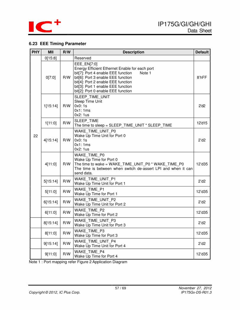
IP175G/GI/GH/GHI Data Sheet
57 / 69 November 27, 2012
Copyright © 2012, IC Plus Corp. IP175Gx-DS-R01.3
6.23 EEE Timing Parameter
PHY MII R/W Description Default
0[15:8] Reserved
0[7:0] R/W
EEE_EN[7:0] Energy Efficient Ethernet Enable for each port bit[7]: Port 4 enable EEE function Note 1 bit[6]: Port 3 enable EEE function bit[4]: Port 2 enable EEE function bit[3]: Port 1 enable EEE function bit[2]: Port 0 enable EEE function
8’hFF
1[15:14] R/W
SLEEP_TIME_UNIT Sleep Time Unit 0x0: 1s 0x1: 1ms 0x2: 1us
2’d2
1[11:0] R/W SLEEP_TIME The time to sleep = SLEEP_TIME_UNIT * SLEEP_TIME
12’d15
4[15:14] R/W
WAKE_TIME_UNIT_P0 Wake Up Time Unit for Port 0 0x0: 1s 0x1: 1ms 0x2: 1us
2’d2
4[11:0] R/W
WAKE_TIME_P0 Wake Up Time for Port 0 The time to wake = WAKE_TIME_UNIT_P0 * WAKE_TIME_P0 The time is between when switch de-assert LPI and when it can send data.
12’d35
5[15:14] R/W WAKE_TIME_UNIT_P1 Wake Up Time Unit for Port 1
2’d2
5[11:0] R/W WAKE_TIME_P1 Wake Up Time for Port 1
12’d35
6[15:14] R/W WAKE_TIME_UNIT_P2 Wake Up Time Unit for Port 2
2’d2
22
6[11:0] R/W WAKE_TIME_P2 Wake Up Time for Port 2
12’d35
8[15:14] R/W WAKE_TIME_UNIT_P3 Wake Up Time Unit for Port 3
2’d2
8[11:0] R/W WAKE_TIME_P3 Wake Up Time for Port 3
12’d35
9[15:14] R/W WAKE_TIME_UNIT_P4 Wake Up Time Unit for Port 4
2’d2
9[11:0] R/W WAKE_TIME_P4 Wake Up Time for Port 4
12’d35
Note 1 : Port mapping refer Figure 2 Application Diagram

IP175G/GI/GH/GHI Data Sheet
58 / 69 November 27, 2012
Copyright © 2012, IC Plus Corp. IP175Gx-DS-R01.3
6.24 WOL (Wake on LAN)
PHY MII R/W Description Default
10[15:8] R/W WOL_EN[7:0] Wake on lan enable for each port
P(8’hff)
10[7:2] R/W RESERVED
22
10[1:0] R/W
WOL_TIMER 0x0: disable 0x1: 3min 0x2: 5min 0x3: 10min
2’b0
Note 1 : Port mapping refer Figure 2 Application Diagram 6.25 Link Aggregation
PHY MII R/W Description Default
11[15:5] RESERVED
11[4:3] R/W
AGGR_IDX_SEL Aggregation Index Selection 2’b00: index[2:0] 2’b01: {index[3], index[1:0]} 2’b10: {index[3:2], index[0]} 2’b11: index[3:1]
2’b00
11[2:0] R/W
AGGR_MODE Aggregation Mode 3’b000: SMAC 3’b001: DMAC 3’b010: SMAC xor DMAC 3’b011: Source port
3’b000
12[7:0] R/W AGGR_GROUP0 Aggregation Group 0
8’h00
13[7:0] R/W AGGR_GROUP1 Aggregation Group 1
8’h00
16[7:0] R/W AGGR_MASK0 Aggregation Port Mask 0 Only one port can be selected in each aggregation group
8’hFF
17[7:0] R/W AGGR_MASK1 Aggregation Port Mask 1
8’hFF
18[7:0] R/W AGGR_MASK2 Aggregation Port Mask 2
8’hFF
20[7:0] R/W AGGR_MASK3 Aggregation Port Mask 3
8’hFF
22
21[7:0] R/W AGGR_MASK4 Aggregation Port Mask 4
8’hFF

IP175G/GI/GH/GHI Data Sheet
59 / 69 November 27, 2012
Copyright © 2012, IC Plus Corp. IP175Gx-DS-R01.3
6.26 VLAN Group Control Register
6.26.1 VLAN Classification
PHY MII R/W Description Default
0[15] R/W (SC)
VLAN_TABLE_CLR Clear the contents of VLAN TABLE register 1: clear register 0: do nothing (default) Self-clear after set and register cleared
1’b0
0[14] RESERVED
0[13] R/W
UNVID_MODE Unknown-VID Mode 0: discard 1 : flood packet
1’b0
0[12:0] RESERVED
1[15:8] R/W
VLAN_CLS[7:0] VLAN Classification associated with each port Only active at tagged-based VLAN 0 : use VID to classify VLAN -use VID to search VLAN table if tag packet -use PVID to search VLAN table if untag packet 1 : use PVID to classify VLAN -always use PVID to search VLAN table
8’h00
23
1[7:0] TAG_VLAN_EN Tag-based VLAN enable
8’h00
6.26.2 VLAN Ingress Rule
PHY MII R/W Description Default
2[15:14] RESERVED
2[13] R/W VLAN_DROP_CFI Drop incoming frame, if the CFI field is not equal to zero.
1’b0
RSVD_VID[2:0] Reserved VID
Bit 0
The null VID. If set, frames with null VID (priority-tagged frame) treat as untagged frames. 0: disable 1: enable (default)
Bit 1
VID=1 (default VID) Replace default VID with PVID 0: disable (default) 1: enable
23
2[12:10] R/W
Bit 2
VID=FFF Discard frame if the VID is the value FFF 0: disable(default) 1: enable
3’b001

IP175G/GI/GH/GHI Data Sheet
60 / 69 November 27, 2012
Copyright © 2012, IC Plus Corp. IP175Gx-DS-R01.3
PHY MII R/W Description Default
2[9:8] R/W
ACCEPTABLE_FRM_TYPE[1:0] Acceptable Frame Type 2’b00 Admit all frames (default) 2’b01 Admit VLAN-tagged frames 2’b10 Admit Untagged frames 2’b11 Reserved
2’b00
2[7:0] R/W
VLAN_INGRESS_FILTER[7:0] VLAN Ingress Filter associated with each port If ingress filter for a given port is set, frame shall discard on that port whose VLAN classification does not include that port in it member set.
8’hFF
23 3 RESERVED
6.26.3 Default VLAN Information
PHY MII R/W Description Default
7[15:0] R/W VLAN_INFO_0. Port 2 default VLAN information value (PVID_0)
16’h0001
8[15:0] R/W VLAN_INFO_1. Port 3 default VLAN information value (PVID_1)
16’h0001
9[15:0] R/W VLAN_INFO_2. Port 4 default VLAN information value (PVID_2)
16’h0001
11[15:0] R/W VLAN_INFO_3. Port 6 default VLAN information value (PVID_3)
16’h0001
23
12[15:0] R/W VLAN_INFO_4. Port 7 default VLAN information value (PVID_4)
16’h0001
6.26.4 VLAN TAG Control Register
PHY MII R/W Description Default
13[7:0] R/W
ADD_TAG[7:0] Note 1 Port x adds a VLAN tag of each outgoing packet Bit 0: Port0 Bit 1: Port1 … Bit7: Port7
8’h00
23
14[7:0] R/W
REMOVE_TAG[7:0] Note 1 Port x removes the VLAN tag of each outgoing packet Bit 0: Port0 Bit 1: Port1 … Bit 7: Port7
8’h00
Note 1 : Port mapping refer Figure 2 Application Diagram

IP175G/GI/GH/GHI Data Sheet
61 / 69 November 27, 2012
Copyright © 2012, IC Plus Corp. IP175Gx-DS-R01.3
6.26.5 Port Based VLAN Member Register
PHY MII R/W Description Default
16[7:0] R/W PBV_MEMBER_P0[7:0] Port based VLAN member port VLAN member port associated with the Port0.
8’hFF
16[15:8] R/W PBV_MEMBER_P1[7:0] Port based VLAN member port VLAN member port associated with the Port1.
8’hFF
17[7:0] R/W PBV_MEMBER_P2[7:0] Port based VLAN member port VLAN member port associated with the Port2.
8’hFF
18[7:0] R/W PBV_MEMBER_P3[7:0] Port based VLAN member port VLAN member port associated with the Port3.
8’hFF
18[15:8] R/W PBV_MEMBER_P4[7:0] Port based VLAN member port VLAN member port associated with the Port4.
8’hFF
6.26.6 Leaky VLAN Control Register
PHY MII R/W Description Default
19[15:3] RESERVED
23 19[2:0] R/W
LEAKY_VLAN[2:0] Bit0: ARP leaky VLAN Bit1: Unicast forwarding leaky VLAN, DA=individual MAC & DA match was found Bit2: Multicast leaky VLAN
2’b00
6.27 VLAN Table
6.27.1 VLAN Control Register
PHY MII R/W Description Default
24
0[15:0] R/W VLAN_VALID[15:0] VALN filter is valid. The VALN filter entry X is valid associated with the VID_X.
16’h 0000
6.27.2 VLAN Identifier Register
PHY MII R/W Description Default
1[11:0] R/W VID_0[11:0] VLAN identifier associated with VALN 0.
12’h001
2[11:0] R/W VID_1[11:0] VLAN identifier associated with VALN 1.
12’h002
3[11:0] R/W VID_2[11:0] VLAN identifier associated with VALN 2.
12’h003
4[11:0] R/W VID_3[11:0] VLAN identifier associated with VALN 3.
12’h004
24
5[11:0] R/W VID_4[11:0] VLAN identifier associated with VALN 4.
12’h005
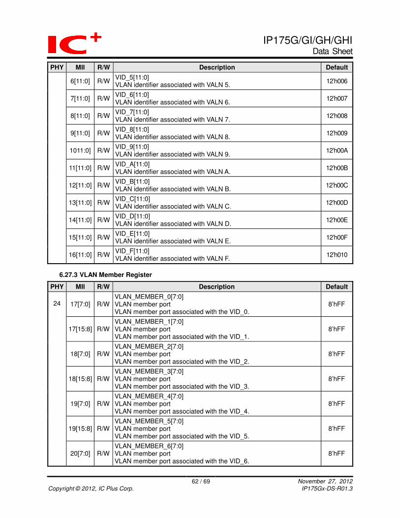
IP175G/GI/GH/GHI Data Sheet
62 / 69 November 27, 2012
Copyright © 2012, IC Plus Corp. IP175Gx-DS-R01.3
PHY MII R/W Description Default
6[11:0] R/W VID_5[11:0] VLAN identifier associated with VALN 5.
12’h006
7[11:0] R/W VID_6[11:0] VLAN identifier associated with VALN 6.
12’h007
8[11:0] R/W VID_7[11:0] VLAN identifier associated with VALN 7.
12’h008
9[11:0] R/W VID_8[11:0] VLAN identifier associated with VALN 8.
12’h009
1011:0] R/W VID_9[11:0] VLAN identifier associated with VALN 9.
12’h00A
11[11:0] R/W VID_A[11:0] VLAN identifier associated with VALN A.
12’h00B
12[11:0] R/W VID_B[11:0] VLAN identifier associated with VALN B.
12’h00C
13[11:0] R/W VID_C[11:0] VLAN identifier associated with VALN C.
12’h00D
14[11:0] R/W VID_D[11:0] VLAN identifier associated with VALN D.
12’h00E
15[11:0] R/W VID_E[11:0] VLAN identifier associated with VALN E.
12’h00F
16[11:0] R/W VID_F[11:0] VLAN identifier associated with VALN F.
12’h010
6.27.3 VLAN Member Register
PHY MII R/W Description Default
17[7:0] R/W VLAN_MEMBER_0[7:0] VLAN member port VLAN member port associated with the VID_0.
8’hFF
17[15:8] R/W VLAN_MEMBER_1[7:0] VLAN member port VLAN member port associated with the VID_1.
8’hFF
18[7:0] R/W VLAN_MEMBER_2[7:0] VLAN member port VLAN member port associated with the VID_2.
8’hFF
18[15:8] R/W VLAN_MEMBER_3[7:0] VLAN member port VLAN member port associated with the VID_3.
8’hFF
19[7:0] R/W VLAN_MEMBER_4[7:0] VLAN member port VLAN member port associated with the VID_4.
8’hFF
19[15:8] R/W VLAN_MEMBER_5[7:0] VLAN member port VLAN member port associated with the VID_5.
8’hFF
24
20[7:0] R/W VLAN_MEMBER_6[7:0] VLAN member port VLAN member port associated with the VID_6.
8’hFF
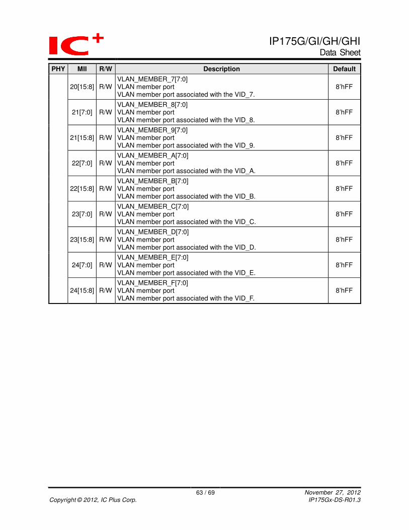
IP175G/GI/GH/GHI Data Sheet
63 / 69 November 27, 2012
Copyright © 2012, IC Plus Corp. IP175Gx-DS-R01.3
PHY MII R/W Description Default
20[15:8] R/W VLAN_MEMBER_7[7:0] VLAN member port VLAN member port associated with the VID_7.
8’hFF
21[7:0] R/W VLAN_MEMBER_8[7:0] VLAN member port VLAN member port associated with the VID_8.
8’hFF
21[15:8] R/W VLAN_MEMBER_9[7:0] VLAN member port VLAN member port associated with the VID_9.
8’hFF
22[7:0] R/W VLAN_MEMBER_A[7:0] VLAN member port VLAN member port associated with the VID_A.
8’hFF
22[15:8] R/W VLAN_MEMBER_B[7:0] VLAN member port VLAN member port associated with the VID_B.
8’hFF
23[7:0] R/W VLAN_MEMBER_C[7:0] VLAN member port VLAN member port associated with the VID_C.
8’hFF
23[15:8] R/W VLAN_MEMBER_D[7:0] VLAN member port VLAN member port associated with the VID_D.
8’hFF
24[7:0] R/W VLAN_MEMBER_E[7:0] VLAN member port VLAN member port associated with the VID_E.
8’hFF
24[15:8] R/W VLAN_MEMBER_F[7:0] VLAN member port VLAN member port associated with the VID_F.
8’hFF

IP175G/GI/GH/GHI Data Sheet
64 / 69 November 27, 2012
Copyright © 2012, IC Plus Corp. IP175Gx-DS-R01.3
7 Electrical Characteristics
7.1 Absolute Maximum Rating
Stresses exceed those values listed under Absolute Maximum Ratings may cause permanent damage to the device. Functional performance and device reliability are not guaranteed under these conditions. All voltages are specified with respect to GND.
Supply Voltage – 0.3V to 3.63V Input Voltage – 0.3V to 3.63V Output Voltage – 0.3V to 3.63V Storage Temperature – 65°C to 150°C Ambient Operating Temperature (Ta) (IP175G/GH) 0°C to 70°C IC Junction Temperature (Tj) (IP175G/GH) 0°C to 125°C Ambient Operating Temperature (Ta) (IP175G/GHI) – 40°C to 85°C IC Junction Temperature (Tj) (IP175 GI) – 40°C to 125°C
7.2 DC Characteristic
Operating Conditions
Parameter Sym. Min. Typ. Max. Unit Conditions
Core Supply Voltage DVDD
Analog Low Supply Voltage AV10 1.05 1.1 1.23
Analog High Supply Voltage AV33
I/O Pad Supply Voltage PVDD 3 3.3 3.6
V
P100MF 520 All port link 100M Full activ
P10MF 488 All port link 10M Full activ Power Consumption
PIDLE 125
mW
All port unlink
Input Clock
Parameter Sym. Min. Typ. Max. Unit Conditions
Frequency F 25 MHz
Frequency Tolerance FT -50 +50 PPM
I/O Electrical Characteristics
Parameter Sym Min. Max. Unit Conditions
Input Low Voltage -LED PAD direct mode -LED PAD bicolor mode -NOT LED PAD
VIL
0.39*PVDD 0.36*PVDD 0.4*PVDD
Input High Voltage -LED PAD direct mode -LED PAD bicolor mode -NOT LED PAD
VIH
0.58*PVDD 0.58*PVDD 0.6*PVDD
X1 Input Low Voltage VILX1 0.6
X1 Input High Voltage VIHX1 1.5
Output Low Voltage VOL 0.4
Output High Voltage VOH 2.4
RESETB Threshold Voltage VRST 0.4*PVDD 0.6*PVDD
V

IP175G/GI/GH/GHI Data Sheet
65 / 69 November 27, 2012
Copyright © 2012, IC Plus Corp. IP175Gx-DS-R01.3
7.3 AC Timing
7.3.1 Power On Sequence and Reset Timing
Description Min. Typ. Max. Unit
X1 valid period before reset released 10 - - ms
Reset period 10 - - ms
All power source ready before reset released 10 ms
Time difference between VCC3.3 and VCC1.0 (Tdiff) -2 ms
8 Crystal Specifications
Item Parameter Range
1 Nominal Frequency 25.000 MHz
2 Oscillation Mode Fundamental Mode
3 Frequency Tolerance at 25℃ +/- 50 ppm
4 Temperature Characteristics +/- 50 ppm
5 Operating Temperature Range -10℃ ~ +70℃
6 Equivalent Series Resistance 40 ohm Max.
7 Drive Level 100μW
8 Load Capacitance 20 pF
9 Shunt Capacitance 7 pF Max
10 Insulation Resistance Mega ohm Min./DC 100V
11 Aging Rate A Year +/- 5 ppm/year
3.3V Power
1.0V Power
OSCI (X1)
RESET X1 vaild period before reset relaesed
RESET period
2.1ms
OSC stable
RESET released
Tdiff

IP175G/GI/GH/GHI Data Sheet
66 / 69 November 27, 2012
Copyright © 2012, IC Plus Corp. IP175Gx-DS-R01.3
Serial Management Imierface Timing
Symbol Description Min. Typ. Max. Unit
Tch MDC High Time 200 - - ns
Tcl MDC Low Time 200 - - ns
Tcm MDC period 400 - - ns
Tmd MDIO output delay - - 20 ns
Tmh MDIO setup time 10 - - ns
Tms MDIO hold time 10 - - ns
M D C
M D IO
T m s T m h
W rite C yc le
T c l T ch
T c m
T m d
M D C
M D IO
R ea d C yc le

IP175G/GI/GH/GHI Data Sheet
67 / 69 November 27, 2012
Copyright © 2012, IC Plus Corp. IP175Gx-DS-R01.3
8.1.1 EEPROM Timing
8.1.1.1 Data read cycle
Symbol Description Min. Typ. Max. Unit
TSCL Receive clock period - 20480 - ns
TsSCL SDA to SCL setup time 2 - - ns
ThSCL SDA to SCL hold time 0.5 - - ns
Read data cycle
SCL
SDA
T sSCL
T hSCL
TSCL
8.1.1.2 Command cycle
Symbol Description Min. Typ. Max. Unit
TSCL Transmit clock period - 20480 - ns
TdSCL SCL falling edge to SDA - - 5200 ns
Comand cycle
TdSCL
SCL
SDA
TSCL
8.2 Thermal Data
Theta Ja Theta Jc Conditions Units
30.7~32.5 11.6~12.4 2 Layer PCB oC/W
25.0~26.6 11.1~11.7 4 Layer PCB oC/W

IP175G/GI/GH/GHI Data Sheet
68 / 69 November 27, 2012
Copyright © 2012, IC Plus Corp. IP175Gx-DS-R01.3
9 Order Information
Part No. Package Operating Temperature Notice
IP175G/GH 48-Lead QFN 0°C to 70°C
IP175GI/GHI 48-Lead QFN -40°C to 85°C

IP175G/GI/GH/GHI Data Sheet
69 / 69 November 27, 2012
Copyright © 2012, IC Plus Corp. IP175Gx-DS-R01.3
10 Package Detail
10.1 48 QFN Outline Dimensions